US6197683B1 - Method of forming metal nitride film by chemical vapor deposition and method of forming metal contact of semiconductor device using the same - Google Patents
Method of forming metal nitride film by chemical vapor deposition and method of forming metal contact of semiconductor device using the sameDownload PDFInfo
- Publication number
- US6197683B1 US6197683B1US09/156,724US15672498AUS6197683B1US 6197683 B1US6197683 B1US 6197683B1US 15672498 AUS15672498 AUS 15672498AUS 6197683 B1US6197683 B1US 6197683B1
- Authority
- US
- United States
- Prior art keywords
- metal
- deposition chamber
- nitride film
- source
- forming
- Prior art date
- Legal status (The legal status is an assumption and is not a legal conclusion. Google has not performed a legal analysis and makes no representation as to the accuracy of the status listed.)
- Expired - Lifetime
Links
Images


Classifications
- H—ELECTRICITY
- H01—ELECTRIC ELEMENTS
- H01L—SEMICONDUCTOR DEVICES NOT COVERED BY CLASS H10
- H01L21/00—Processes or apparatus adapted for the manufacture or treatment of semiconductor or solid state devices or of parts thereof
- H01L21/70—Manufacture or treatment of devices consisting of a plurality of solid state components formed in or on a common substrate or of parts thereof; Manufacture of integrated circuit devices or of parts thereof
- H01L21/71—Manufacture of specific parts of devices defined in group H01L21/70
- H01L21/768—Applying interconnections to be used for carrying current between separate components within a device comprising conductors and dielectrics
- H01L21/76838—Applying interconnections to be used for carrying current between separate components within a device comprising conductors and dielectrics characterised by the formation and the after-treatment of the conductors
- H01L21/76841—Barrier, adhesion or liner layers
- H01L21/76843—Barrier, adhesion or liner layers formed in openings in a dielectric
- C—CHEMISTRY; METALLURGY
- C23—COATING METALLIC MATERIAL; COATING MATERIAL WITH METALLIC MATERIAL; CHEMICAL SURFACE TREATMENT; DIFFUSION TREATMENT OF METALLIC MATERIAL; COATING BY VACUUM EVAPORATION, BY SPUTTERING, BY ION IMPLANTATION OR BY CHEMICAL VAPOUR DEPOSITION, IN GENERAL; INHIBITING CORROSION OF METALLIC MATERIAL OR INCRUSTATION IN GENERAL
- C23C—COATING METALLIC MATERIAL; COATING MATERIAL WITH METALLIC MATERIAL; SURFACE TREATMENT OF METALLIC MATERIAL BY DIFFUSION INTO THE SURFACE, BY CHEMICAL CONVERSION OR SUBSTITUTION; COATING BY VACUUM EVAPORATION, BY SPUTTERING, BY ION IMPLANTATION OR BY CHEMICAL VAPOUR DEPOSITION, IN GENERAL
- C23C16/00—Chemical coating by decomposition of gaseous compounds, without leaving reaction products of surface material in the coating, i.e. chemical vapour deposition [CVD] processes
- C23C16/22—Chemical coating by decomposition of gaseous compounds, without leaving reaction products of surface material in the coating, i.e. chemical vapour deposition [CVD] processes characterised by the deposition of inorganic material, other than metallic material
- C23C16/30—Deposition of compounds, mixtures or solid solutions, e.g. borides, carbides, nitrides
- C23C16/34—Nitrides
- C—CHEMISTRY; METALLURGY
- C23—COATING METALLIC MATERIAL; COATING MATERIAL WITH METALLIC MATERIAL; CHEMICAL SURFACE TREATMENT; DIFFUSION TREATMENT OF METALLIC MATERIAL; COATING BY VACUUM EVAPORATION, BY SPUTTERING, BY ION IMPLANTATION OR BY CHEMICAL VAPOUR DEPOSITION, IN GENERAL; INHIBITING CORROSION OF METALLIC MATERIAL OR INCRUSTATION IN GENERAL
- C23C—COATING METALLIC MATERIAL; COATING MATERIAL WITH METALLIC MATERIAL; SURFACE TREATMENT OF METALLIC MATERIAL BY DIFFUSION INTO THE SURFACE, BY CHEMICAL CONVERSION OR SUBSTITUTION; COATING BY VACUUM EVAPORATION, BY SPUTTERING, BY ION IMPLANTATION OR BY CHEMICAL VAPOUR DEPOSITION, IN GENERAL
- C23C16/00—Chemical coating by decomposition of gaseous compounds, without leaving reaction products of surface material in the coating, i.e. chemical vapour deposition [CVD] processes
- C23C16/44—Chemical coating by decomposition of gaseous compounds, without leaving reaction products of surface material in the coating, i.e. chemical vapour deposition [CVD] processes characterised by the method of coating
- C23C16/455—Chemical coating by decomposition of gaseous compounds, without leaving reaction products of surface material in the coating, i.e. chemical vapour deposition [CVD] processes characterised by the method of coating characterised by the method used for introducing gases into reaction chamber or for modifying gas flows in reaction chamber
- C23C16/45523—Pulsed gas flow or change of composition over time
- C23C16/45525—Atomic layer deposition [ALD]
- C23C16/45553—Atomic layer deposition [ALD] characterized by the use of precursors specially adapted for ALD
- H—ELECTRICITY
- H01—ELECTRIC ELEMENTS
- H01L—SEMICONDUCTOR DEVICES NOT COVERED BY CLASS H10
- H01L21/00—Processes or apparatus adapted for the manufacture or treatment of semiconductor or solid state devices or of parts thereof
- H01L21/02—Manufacture or treatment of semiconductor devices or of parts thereof
- H01L21/04—Manufacture or treatment of semiconductor devices or of parts thereof the devices having potential barriers, e.g. a PN junction, depletion layer or carrier concentration layer
- H01L21/18—Manufacture or treatment of semiconductor devices or of parts thereof the devices having potential barriers, e.g. a PN junction, depletion layer or carrier concentration layer the devices having semiconductor bodies comprising elements of Group IV of the Periodic Table or AIIIBV compounds with or without impurities, e.g. doping materials
- H01L21/28—Manufacture of electrodes on semiconductor bodies using processes or apparatus not provided for in groups H01L21/20 - H01L21/268
- H01L21/283—Deposition of conductive or insulating materials for electrodes conducting electric current
- H01L21/285—Deposition of conductive or insulating materials for electrodes conducting electric current from a gas or vapour, e.g. condensation
- H01L21/28506—Deposition of conductive or insulating materials for electrodes conducting electric current from a gas or vapour, e.g. condensation of conductive layers
- H01L21/28512—Deposition of conductive or insulating materials for electrodes conducting electric current from a gas or vapour, e.g. condensation of conductive layers on semiconductor bodies comprising elements of Group IV of the Periodic Table
- H01L21/28556—Deposition of conductive or insulating materials for electrodes conducting electric current from a gas or vapour, e.g. condensation of conductive layers on semiconductor bodies comprising elements of Group IV of the Periodic Table by chemical means, e.g. CVD, LPCVD, PECVD, laser CVD
- H01L21/28562—Selective deposition
- H—ELECTRICITY
- H01—ELECTRIC ELEMENTS
- H01L—SEMICONDUCTOR DEVICES NOT COVERED BY CLASS H10
- H01L21/00—Processes or apparatus adapted for the manufacture or treatment of semiconductor or solid state devices or of parts thereof
- H01L21/02—Manufacture or treatment of semiconductor devices or of parts thereof
- H01L21/04—Manufacture or treatment of semiconductor devices or of parts thereof the devices having potential barriers, e.g. a PN junction, depletion layer or carrier concentration layer
- H01L21/18—Manufacture or treatment of semiconductor devices or of parts thereof the devices having potential barriers, e.g. a PN junction, depletion layer or carrier concentration layer the devices having semiconductor bodies comprising elements of Group IV of the Periodic Table or AIIIBV compounds with or without impurities, e.g. doping materials
- H01L21/28—Manufacture of electrodes on semiconductor bodies using processes or apparatus not provided for in groups H01L21/20 - H01L21/268
- H01L21/283—Deposition of conductive or insulating materials for electrodes conducting electric current
- H01L21/285—Deposition of conductive or insulating materials for electrodes conducting electric current from a gas or vapour, e.g. condensation
- H01L21/28506—Deposition of conductive or insulating materials for electrodes conducting electric current from a gas or vapour, e.g. condensation of conductive layers
- H01L21/28512—Deposition of conductive or insulating materials for electrodes conducting electric current from a gas or vapour, e.g. condensation of conductive layers on semiconductor bodies comprising elements of Group IV of the Periodic Table
- H01L21/28568—Deposition of conductive or insulating materials for electrodes conducting electric current from a gas or vapour, e.g. condensation of conductive layers on semiconductor bodies comprising elements of Group IV of the Periodic Table the conductive layers comprising transition metals
- H—ELECTRICITY
- H01—ELECTRIC ELEMENTS
- H01L—SEMICONDUCTOR DEVICES NOT COVERED BY CLASS H10
- H01L21/00—Processes or apparatus adapted for the manufacture or treatment of semiconductor or solid state devices or of parts thereof
- H01L21/70—Manufacture or treatment of devices consisting of a plurality of solid state components formed in or on a common substrate or of parts thereof; Manufacture of integrated circuit devices or of parts thereof
- H01L21/71—Manufacture of specific parts of devices defined in group H01L21/70
- H01L21/768—Applying interconnections to be used for carrying current between separate components within a device comprising conductors and dielectrics
- H01L21/76801—Applying interconnections to be used for carrying current between separate components within a device comprising conductors and dielectrics characterised by the formation and the after-treatment of the dielectrics, e.g. smoothing
- H01L21/76802—Applying interconnections to be used for carrying current between separate components within a device comprising conductors and dielectrics characterised by the formation and the after-treatment of the dielectrics, e.g. smoothing by forming openings in dielectrics
- H01L21/76804—Applying interconnections to be used for carrying current between separate components within a device comprising conductors and dielectrics characterised by the formation and the after-treatment of the dielectrics, e.g. smoothing by forming openings in dielectrics by forming tapered via holes
- H—ELECTRICITY
- H10—SEMICONDUCTOR DEVICES; ELECTRIC SOLID-STATE DEVICES NOT OTHERWISE PROVIDED FOR
- H10D—INORGANIC ELECTRIC SEMICONDUCTOR DEVICES
- H10D1/00—Resistors, capacitors or inductors
- H10D1/01—Manufacture or treatment
- H10D1/041—Manufacture or treatment of capacitors having no potential barriers
- H10D1/042—Manufacture or treatment of capacitors having no potential barriers using deposition processes to form electrode extensions
- H—ELECTRICITY
- H10—SEMICONDUCTOR DEVICES; ELECTRIC SOLID-STATE DEVICES NOT OTHERWISE PROVIDED FOR
- H10D—INORGANIC ELECTRIC SEMICONDUCTOR DEVICES
- H10D1/00—Resistors, capacitors or inductors
- H10D1/60—Capacitors
- H10D1/68—Capacitors having no potential barriers
- H10D1/692—Electrodes
- H10D1/711—Electrodes having non-planar surfaces, e.g. formed by texturisation
- H10D1/716—Electrodes having non-planar surfaces, e.g. formed by texturisation having vertical extensions
Definitions
- the present inventionrelates to a method of fabricating semiconductor devices, and more particularly, to a method of forming a metal nitride film by chemical vapor deposition (CVD) where a metal source and a nitrogen source are used as a precursor, and a method of forming a metal contact of a semiconductor device using the above method.
- CVDchemical vapor deposition
- a barrier metal layerwhich prevents mutual diffusion or chemical reaction between different materials, is indispensable to stabilize the contact interfaces of semiconductor devices.
- a metal nitridesuch as TiN, TaN or WN has been widely used as the barrier metal layer of semiconductor devices.
- TiNis a representative example among the above metal nitrides.
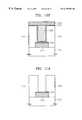
- FIGS. 9A and 9Bshow the cross-section of a via contact for connection between metal wiring.
- FIGS. 9A and 9Bshow a simple via contact and an anchor via contact, respectively.
- the formation processes thereofare as follows.
- a first metal layer 30 composed of aluminum (Al)is formed on a semiconductor substrate 20 .
- a TiN film 40is formed as a capping film on the resultant structure by sputtering, and then an interlayer insulative film 50 or 51 is deposited.
- a contact holeis formed by etching the interlayer insulative film 50 or 51 on the first metal layer 30 .
- the step of forming an anchor A by wet etchingis added.
- a tungsten (W) plug 70 or 71is formed to fill the contact hole, by CVD.
- tungsten at the upper portionis removed by chemical mechanical polishing or etch-back, and then a second metal layer is deposited on the resultant structure, thereby completing the connection between metal wiring.
- this last stepis not shown.
- the TiN film 60 or 61being the barrier metal layer, is deposited by sputtering, with inferior step coverage.
- the thickness of a TiN film on the bottom, corner and anchor A of the contact holeis reduced, with an increase in the aspect ratio of the via. Accordingly, at a thin portion, Ti or Al combines with fluorine remaining in tungsten source gas WF 6 during tungsten deposition being a subsequent process, and thus an insulative film X forms of TiF x or AlF x leading to a contact failure.
- a process for fabricating a metal nitride film using CVD(hereinafter called a CVD-metal nitride film) has been developed as a next generation process.
- a general process for forming a CVD-metal nitride filmuses a metal source containing chlorine (Cl), e.g., a precursor such as titanium chloride TiCI 4 .
- a metal source containing chlorine (Cl)e.g., a precursor such as titanium chloride TiCI 4 .
- the CVD-metal nitride film using TiCI 4 as the precursorhas a high step coverage of 95% or higher and is quickly deposited, but Cl remains in the metal nitride film as impurities.
- the Cl remaining as impurities in the metal nitride filmcauses corrosion of metal wiring such as Al and increases resistivity.
- the Cl content in the metal nitride filmmust be reduced and the resistivity must be lowered, by deposition at high temperature.
- a deposition temperature of 600° C. or moreexceeds thermal budget and thermal stress limits which an underlayer can withstand.
- a deposition temperature of 480° C. or loweris required, so that a high temperature CVD-metal nitride film process cannot be used.
- a low temperature deposition CVD-metal nitride film processis possible, by adding MH (methylhydrazine, (CH 3 )HNNH 2 ) to the metal source such as TICl 4 , but this method has a defect in that step coverage is decreased to 70% or lower.
- MOCVD-metal nitride filmAnother method capable of low temperature deposition is to form a MOCVD-metal nitride film using a metalorganic precursor such as TDEAT (tetrakis diethylamino Ti, Ti(N(CH 2 CH 3 ) 2 ) 4 ), or TDMAT (tetrakis dimethylamino Ti, Ti(N(CH 3 ) 2 ) 4 ).
- TDEATtetrakis diethylamino Ti, Ti(N(CH 2 CH 3 ) 2 ) 4 ), or TDMAT (tetrakis dimethylamino Ti, Ti(N(CH 3 ) 2 ) 4 ).
- TDEATtetrakis diethylamino Ti, Ti(N(CH 2 CH 3 ) 2 ) 4
- TDMATtetrakis dimethylamino Ti, Ti(N(CH 3 ) 2 ) 4
- the MOCVD-metal nitride film
- a method of forming a metal nitride film using atomic layer epitaxy (ALE)has been tried as an alternative to deposition, in order to overcome the problems due to Cl.
- ALEatomic layer epitaxy
- the ALEgrows the metal nitride film in units of an atomic layer using only chemical adsorption, and the deposition speed (0.25 ⁇ /cycle or less) is too slow to apply the ALE to mass production.
- a method of forming a metal nitride film using chemical vapor deposition (CVD) in which a metal source and a nitrogen source are used as precursorsin which a metal source and a nitrogen source are used as precursors.
- CVDchemical vapor deposition
- a semiconductor substrateis introduced into a deposition chamber, and the metal source flows into the deposition chamber.
- the flow of metal sourceis stopped, and a flow of purge gas is introduced into the deposition chamber.
- the purge gasis cut off and the nitrogen source gas flows into the deposition chamber to react with the metal source gas adsorbed on the semiconductor substrate.
- the nitrogen source gas remaining in the deposition chamberis removed by cutting off the inflow of the nitrogen source and flowing the purge gas into the deposition chamber.
- the metal nitride filmis formed on the semiconductor substrate.
- a gas inflow cycle of a sequence of the metal source, the purge gas, the nitrogen source, and the purge gascan be repeated until a metal nitride film having a desired thickness is obtained.
- a titanium nitride film TiNcan be formed by using TiCl 4 (titanium chloride), TiCl 3 (titanium chloride), Til 4 (titanium iodide), TiBr 2 (titanium bromide), TiF 4 (titaniumfluoride), (C 5 H 5 ) 2 TiCl 2 (bis(cyclopentadienyl)titanium dichloride), ((CH 3 ) 5 C 5 ) 2 TiCl 2 (bis(pentamethylcyclopentadienyl) titanium dichloride), C 5 H 5 TiCl 3 (cyclopentadienyltitanium trichloride), C 9 H 10 BCl 3 N 6 Ti (hydrotris (1 -pyrazolylborato) trichloro titanium), C 9 H 7 TiCl 3 (indenyltitanium trichloride), (C 5 (CH 3 ) 5 )TiCl 3 (pentamethylcyclo
- a tantalum nitride film TaNcan be formed using a material selected from the group consisting of TaBr 5 (tantalum bromide), TaCl 5 (tantalum chloride), TaF 5 (tantalum fluoride), Tal 5 (Tantalum iodide), and (C 5 (CH 3 ) 5 ) TaCl 4 (pentamethylcyclopentadienyltantalum tetrachloride), as the metal source, and using NH 3 as the nitrogen source.
- TaBr 5tantalum bromide
- TaCl 5tantalum chloride
- TaF 5tantalum fluoride
- Tal 5Tal 5
- Talum iodideTal 5
- C 5 (CH 3 ) 5 ) TaCl 4penentamethylcyclopentadienyltantalum tetrachloride
- the purge gasis an inert gas such as Ar or N 2 .
- 1-5 sccm of the metal sourceflows into the deposition chamber for 1 to 10 seconds
- 5-200 sccm of the nitrogen sourceflows thereinto for 1 to 10 seconds
- 10-200 sccm of the purge gasflows thereinto for 1 to 10 seconds.
- an atmospheric gassuch as Ar, He and N 2 can be continuously introduced into the deposition chamber to maintain a constant pressure in the deposition chamber.
- the TiN filmis formed using TDEAT or TDMAT as the metal source
- the pressure in the deposition chamberis maintained at 1 to 20 torr and the deposition temperature at between 400° C. and 500° C.
- a method of forming a metal contact of a semiconductor devicewherein a first metal layer, an interlayer insulative film, a contact hole, a barrier metal layer, a metal plug, and a second metal layer are sequentially formed on a semiconductor substrate.
- a process for forming the barrier metal layeris as follows. A metal source flows into the semiconductor substrate having the interlayer insulative film in which the contact hole exposing the first metal layer is formed. The metal source is adsorbed to the resultant structure. After a while, the metal source remaining in the deposition chamber is removed by cutting off the inflow of the metal source and flowing a purge gas into the deposition chamber.
- the purge gasis cut off, and a nitrogen source flows into the deposition chamber.
- the nitrogen sourcereacts with the metal source adsorbed on the semiconductor substrate, to thus form a metal nitride film, being the barrier metal layer, on the exposed first metal layer and the contact hole.
- the nitrogen source remaining in the deposition chamberis removed by cutting off the inflow of the nitrogen source and flowing the purge gas into the deposition chamber.
- the barrier metal layer formation processcan be repeated until a barrier metal layer having a desired thickness is obtained.
- a titanium nitride film TiN as the barrier metal layeris formed by using a material selected from the group consisting of TiCl 4 , TiCl 3 , Til 4 , TiBr 2 , TiF 4 , (C 5 H 5 ) 2 TiCl 2 , ((CH 3 ) 5 C 5 ) 2 TiCl 2 , C 5 H 5 TiCl 3 , C 9 H 10 BCl 3 N 6 Ti, C 9 H 7 TiCl 3 , (C 5 CH 3 ) 5 )TiCl 3 , TiCl 4 (NH 3 ) 2 , (CH 3 ) 5 C 5 Ti(CH 3 ) 3 , TDEAT and TDMAT as the metal source, and using NH 3 as the nitrogen source.
- a tantalum nitride film TiN as the barrier metal layeris formed using a material selected from the group consisting of TaBr 5, TaCl 5 , TaF 5 , Tal 5 , and C 5 (CH 3 ) 5 )TaCl 4 as the metal source, and NH 3 as the nitrogen source.
- the purge gasis an inert gas such as Ar or N 2 .
- the flow amounts and flow times of the metal source, nitrogen source, and purge gas flowing into a deposition chamberare within the same ranges as in the above-mentioned method of forming the metal nitride film.
- the pressure within the deposition chamberis kept at about 0.1 to 10 torr when TDEAT or TDMAT is used as the metal source, and about 1 to 20 torr when materials other than TDEAT and TDMAT are used as the metal source.
- the constant pressureis maintained by using an atmospheric gas such as Ar, He, or N 2 .
- a deposition temperature upon the formation of the barrier metal layeris about between 250° C. and 400° C. when TDEAT or TDMAT is used as the metal source, and between 400° C. and 500° C. when materials other than TDEAT and TDMAT are used as the metal source.
- a metal nitride film having low resistivity of 200 ⁇ -cm or less and a low content of Clcan be obtained even with excellent step coverage.
- a CVD-metal nitride filmcan be formed at a temperature of 500° C. or less even at a deposition speed of about 20 ⁇ /cycle, so that the deposition speed of the present invention is higher than that of a metal nitride film formation method using ALE having a growth speed of 0.25 ⁇ /cycle.
- FIG. 1shows a deposition chamber of a chemical vapor deposition (CVD) apparatus for depositing a metal nitride film on a semiconductor substrate, according to the present invention
- FIG. 2shows gas inflow timings for depositing a metal nitride film on a semiconductor substrate, according to the present invention
- FIG. 3is a graph of the results of Rutherford back scattering (RBS) of a metal nitride film deposited according to the present invention
- FIG. 4is a graph illustrating the resistivity and deposition speed of a metal nitride film with respect to flow amount of NH 3 , when the metal nitride film is deposited according to the present invention
- FIG. 5is a graph illustrating the resistivity and deposition speed of a metal nitride film with respect to pressure in a deposition chamber, when the metal nitride film is deposited according to the present invention
- FIG. 6is a graph illustrating the deposited thickness of a metal nitride film versus the number of cycles when the metal nitride film is deposited according to the present invention
- FIG. 7is a graph illustrating the deposition speed of a metal nitride film versus the number of cycles when the metal nitride film is deposited according to the present invention
- FIG. 8is a graph illustrating the resistivity of a metal nitride film versus deposition temperature when the metal nitride film is deposited according to the present invention
- FIGS. 9A and 9Bare cross-sections of a via contact formed by a conventional method
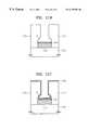
- FIGS. 10A through 10Fare cross-sectional views illustrating an example of a process for forming a via contact using the metal nitride film formation method of the present invention.
- FIGS. 11A through 11Fare cross-sectional views illustrating another example of a process for forming a via contact using the metal nitride film formation method of the present invention.
- FIG. 12is a graph illustrating the relationship between via resistivity and via width when a barrier metal layer is formed according to the present invention and the prior art.
- FIG. 13is a graph illustrating via resistivity distributions when barrier metal layers are formed according to the present invention and the prior art.
- a plurality of gas lines 114 a and 114 b for introducing reaction gases into a deposition chamber 100are installed into the deposition chamber 100 .
- the number of gas linesdepends on the number of metal sources and nitrogen sources, i.e., the number of reaction gases, flowed into the deposition chamber 100 .
- two gas lines 114 a and 114 bare installed.
- the two gas lines 114 a and 114 bhave one end connected to a supply source (not shown) for a metal source and to a supply source (not shown) for a nitrogen source, respectively.
- a TiN filmis deposited on a semiconductor substrate 104
- TiCl 4is used as the metal source
- NH 3is used as the nitrogen source.
- the other ends of the gas lines 114 a and 114 bare connected to a shower head 110 isolated by a predetermined distance (D of FIG. 1) from the semiconductor substrate 104 seated in the deposition chamber 100 .
- reaction gases from the gas supply sourcesenter the deposition chamber 100 via the gas lines 114 a and 114 b and the shower head 110 connected to the ends of the gas lines 114 a and 114 b .
- the reaction gasesreact with each other in the deposition chamber, and the resultant forms a film on the semiconductor substrate 104 .
- the shower head 110is a multi-port shower head which allows the reaction gases to enter the deposition chamber 100 in an unmixed state.
- a two-port shower headis used.
- the gas lines 114 a and 114 bare provided with purge gas supply lines 114 c and 114 d to supply a purge gas to the deposition chamber 100 for exhausting residual gases after reaction.
- Valves 112are installed on the respective gas supply lines. According to the on/off state of the valves 112 , the purge gases or reaction gases may enter into the deposition chamber 100 or be cut off. It is preferable that the valves 112 , such as pneumatic valves, are controlled by a programmed control unit to be periodically turned on or off.
- Reference numeral 102is a heater for heating the semiconductor substrate 104 .
- a method of depositing a metal nitride such as TiN on a semiconductor substrate seated in the deposition chamber of a CVD apparatus having such a configuration, according to the present invention,will now be described in detail referring to FIGS. 1 and 2.
- the semiconductor substrate 104is introduced into the deposition chamber 100 .
- the semiconductor substrate 104may have devices such as transistors formed on its surface (see FIG. 1 ).
- a metal source such as TiCl 4flows into the deposition chamber 100 for the time of t s via the metal source supply line 114 a .
- the metal sourcecan be mixed with a carrier gas such as Ar or N 2 to provide a smooth gas flow into the deposition chamber 100 .
- valves other than the valve of the gas supply line 114 a for supplying a metal sourceare in off state. Accordingly, only the metal source such as TiCl 4 flows into the deposition chamber 100 .
- a part of the entering metal sourceis chemically and physically adsorbed on the surface of the substrate 104 , and the residual remains in the deposition chamber 100 .
- only one type of gasenters the deposition chamber 100 for a predetermined time, instead of simultaneously flowing reaction gases into the deposition chamber 100 . This is called gas pulsing (see FIG. 2 ).
- the valve of the gas supply line 114 a for introducing the metal sourceis closed, and then the valve of the purge gas supply line 114 c is opened to introduce the purge gas such as Ar or N 2 into the deposition chamber 100 for the time of t p , thereby exhausting TiCl 4 gases from the shower head 110 and the deposition chamber 100 (in the purge gas pulsing step of FIG. 2 ).
- the flow of the purge gas and the pressure of the deposition chamberare appropriately controlled to prevent the metal source chemically and physically adsorbed into the semiconductor substrate from being separated and exhausted, thereby exhausting only the source gas remaining within the deposition chamber.
- the valve of the purge gas supply line 114 cis closed, and the valve of the nitrogen gas source supply line 114 b is opened to introduce a nitrogen gas such as NH 3 into the deposition chamber 100 for a time t r .
- the nitrogen gasreacts with the metal source such as TiCl 4 chemically and physically adsorbed into the substrate 104 , thus forming the metal nitride such as TiN on the semiconductor substrate 104 . That is, because of the purge gas pulsing step before the nitrogen source such as NH 3 enters into the deposition chamber 100 , the metal source such as TiCI 4 remaining in the deposition chamber 100 is exhausted via the pump (see FIG. 1 ).
- the nitrogen source such as NH 3does not react with the metal source within the deposition chamber 100 , except for on the semiconductor substrate 104 .
- the metal nitrideis formed on only the semiconductor substrate 104 into which TiCl 4 and NH 3 are adsorbed (in the NH 3 pulsing step of FIG. 2 ).
- the carrier gas such as Ar or N 2can be mixed with the nitrogen gas such as NH 3 for a smooth gas flow into the deposition chamber 100 .
- the residual nitrogen source remaining within the deposition chamber 100 after the reaction with the metal sourceis exhausted by another purge gas pulsing step (in the purge gas pulsing step of FIG. 2 ).
- the pressure in the deposition chamber 100is controlled during the above-described steps. It is preferable that an atmospheric gas such as Ar or N 2 is continuously supplied into the deposition chamber 100 .
- the metal nitride film such as TiN having a predetermined thicknessis deposited through a cycle having a sequence of the TiCl 4 pulsing step, the purge gas pulsing step, the NH 3 pulsing step, and the purge gas pulsing step.
- a deposition speedis about 20 ⁇ /cycle, and when this cycle is repeated, the thickness of a thin film is proportionally increased, so that a thin film having a desired thickness can be deposited on the semiconductor substrate 100 .
- the thickness of the metal nitride film deposited for one cycleis determined by the flow amounts of the metal source and nitrogen source entering the deposition chamber 100 , the gas pulsing times, the flow amount of the purge gas, and the purge time.
- a TiN filmis deposited by the cycles comprising the gas pulsing steps, under the following reaction conditions, on the semiconductor substrate 104 which is maintained at a temperature of 500° C. or lower by the heater 102 of FIG. 1 .
- nitrogen sourceTiCl 4 , NH 3
- carrier gasflow amount of carrier gas: Ar, 10-100 sccm
- FIG. 3shows the results of checking the state of the TiN thin film deposited on the semiconductor substrate 104 under the aforementioned conditions using an RBS method.
- a horizontal axisindicates channels in a multi-channel analyzer (MCA), and a vertical axis indicates the standardized yields of elements detected by the MCA.
- MCAmulti-channel analyzer
- Clis 0.3% or less of the total elements contained in the TiN thin film, which is the detection limit by RBS, as shown in FIG. 3 .
- the resistivity of the TiN film deposited on the semiconductor substrate 104 under the above conditionswas measured as a low value of about 130 ⁇ -cm. Meanwhile, according to several experiments, it was verified that the thickness of the TiN thin film deposited for each cycle preferably is 20 ⁇ or less to provide such an excellent thin film property.
- FIGS. 4 and 5show the resistivity and deposition speed of the TiN film deposited according to the present invention, at various flow amounts of the nitrogen source NH 3 and pressures in the deposition chamber, respectively.
- the deposition speedincreases with an increase in the flow amount of NH 3 and the pressure in the deposition chamber, and thus the resistivity also increases. Accordingly, it is preferable that the conditions for deposition are set in consideration of the thickness and the deposition speed and resistivity of the metal nitride film required according to places to apply the metal nitride film.
- a deposition speed for each cycle, the thickness and deposition speed of a TiN film deposited according to an increase in the number of cycles, and resistivity according to a change in deposition temperature,are measured under four deposition conditions as shown in the following Table 1.
- the metal sourceis TiCl 4
- the nitrogen sourceis NH 3
- the purge gasis Ar.
- TiN 0020 ⁇ /cycle (60 ⁇ /min, since one cycle is 20 seconds)
- TiN 036 ⁇ /cycle (45 ⁇ /min, since one cycle is 8 seconds).
- FIGS. 6 and 7show the deposition thickness and deposition speed, respectively, according to an increase in the number of cycles.
- a deposition temperatureis 500° C.
- the deposition speedincreases slowly with an increase in the number of cycles, and the deposition thickness increases in proportion to the number of cycles.
- the thickness of the TiN film to be depositedcan be controlled by adjusting the number of cycles under consistent deposition conditions.
- FIG. 8is a graph showing resistivity of the TiN film with respect to deposition temperature according to the four deposition conditions described above. It can be seen from FIG. 8 that the resistivity decreases with an increase in the deposition temperature. Particularly, it can be seen that the resistivity sharply decreases under the deposition condition (TiN 00) in which the deposition speed is high. Also, we can recognize that resistivity of 200 ⁇ -cm or less obtained at about 500° C. under all the four deposition conditions.
- metal nitride film formation method of the present inventionis applicable not only to a via contact but also to a metal contact on any substrate. In this case, the process conditions can be changed.
- a first metal layer 210such as Al is formed on a semiconductor substrate 200 , and a TiN film 220 is deposited as a capping film on the resultant structure, as shown in FIG. 10 A.
- the TiN film 220can be deposited by sputtering.
- an interlayer insulative film 230is deposited, and a portion on which a via is to be formed is etched, thereby forming the structure of FIG. 10 B.
- An adhesive layersuch as a thin Ti film is formed on the resultant structure to improve adhesion of the Tin film, before the TiN film, being a barrier metal layer, is deposited.
- This Ti filmcan also be formed by sputtering.
- the TiN film 240being a barrier metal layer, is deposited by the metal nitride film formation method of the present invention, thus forming the structure of FIG. 10 C. That is, as described above, a metal source, a purge gas, and a nitrogen source flow into the deposition apparatus of FIG. 1 in the sequence of the metal source, the purge gas, the nitrogen source, and the purge gas. This is repeated until a desired thickness is obtained.
- the metal sourceis TiCl 4 and the nitrogen source is NH 3 .
- the amounts of the metal source, the nitrogen source and the purge gasare 1 to 5 sccm, 5 to 200 sccm, and 10 to 200 sccm, respectively, and the inflow times thereof are about 1 to 10 seconds.
- a deposition temperatureis 480° C. or lower, and the pressure in the deposition chamber is between 1 torr and 20 torr. If necessary, an atmospheric gas such as Ar, He, or N 2 , and a carrier gas of Ar, N 2 , etc., can be used. These deposition conditions are appropriately controlled considering the deposition apparatus, the deposition speed, the thickness of the TiN film deposited, and the resistivity of the TiN film.
- a metal plug 250 such as Wis formed by a typical method, in FIG. 10D, and a metal deposited on the upper surface of an interlayer insulative film 230 is removed by chemical mechanical polishing or etch back, in FIG. 10 E. Then, when a second metal layer 260 is formed on the resultant structure as shown in FIG. 10F, interconnection between metal layers is accomplished.
- FIGS. 11A through 11Fare cross-sectional views illustrating a process for forming an anchor via contact, which is fundamentally the same as the process of FIGS. 10A through 10F except that an anchor A is formed on the lower portion of a contact hole to lower resistance by increasing a contact area as shown in FIG. 11 B.
- the TiN film 340functions as a stopping layer.
- the anchor Ais formed by wet etching the interlayer insulative film 335 after forming the contact hole as shown in FIG. 11 A.
- the other stepsare the same as those of FIGS. 10A through 10F, so they will not be described again.
- a barrier metal layer having an excellent step coveragecan be obtained at low temperature.
- a contact failure Xsuch as TiFx or AlFx shown in FIGS. 9A and 9B can be prevented.
- a Ti filmis deposited to a thickness of 100 ⁇ on contact holes of various different widths, by sputtering. Then, as a barrier metal layer, a TiN film according to the present invention, and a collimated TiN film formed by sputtering by a conventional method, are deposited to different thicknesses, and a plug is formed of CVD-W.
- the third experimentmeasures via resistance in this case.
- the deposition conditions of the TiN film according to the present inventionare equal to the deposition conditions of TiN 00 of the aforementioned second experiment, with a deposition temperature of 450° C.
- Thickness of TiN film100 ⁇ , 200 ⁇ , 400 ⁇ , 600 ⁇ (these are deposited by the method of the present invention), 700 ⁇ (collimated TiN film)
- resistivitygenerally decreases with an increase in via width as shown in FIG. 12, and resistivity decreases with decreasing the thickness of the TiN film of the present invention.
- the 100 ⁇ -thick TiN film according to the present inventionhas a similar resistance to the collimated TiN film (COL-TiN).
- the via widthis 0.39 ⁇ m
- the above five TiN filmshave similar via resistances.
- the TiN films of the present inventionwere formed at a high deposition speed per cycle (20 ⁇ /cycle) and with large resistivity (300 ⁇ -cm at 450° C.). Accordingly, if the TiN films of the present invention are formed at a lower deposition speed and with smaller resistivity, their via resistances can be significantly improved.
- FIG. 13is a graph showing the distribution of the via resistance of each TiN film when the via width is 0.39 ⁇ m. From the graph of FIG. 13, we can recognize that the collimated TiN film (COL-TiN) and the TiN films according to the present invention are evenly distributed, without a big difference, around 1.0 ⁇ .
- the present inventionhas been described by taking as an example the method wherein the TiN film is formed as a metal nitride film by using TiCl 4 and NH 3 as a precursor.
- the present inventioncan be applied to a TiN film using TICl 3 , Til 4 , TiBr 2 , TiF 4 , (C 5 H 5 ) 2 TiCl 2 , ((CH 3 ) 5 C 5 ) 2 TiCl 2 , C 5 H 5 TiCl 3 , C 9 H 10 BCl 3 N 6 Ti, C 9 H 7 TiCl 3 , (C 5 (CH 3 ) 5 )TiCl 3 , TiCl 4 (NH 3 ) 2 , (CH 3 ) 5 C 5 Ti(CH 3 ) 3 ,TDEAT or TDMAT instead of TiCl 4 as the precursor, and also to other metal nitride films such as TaN firm using TaBr 5 , TaCl 5 , TaF 5 , Tal 5 , or (C 5
- a deposition temperatureis between 250° C. and 400° C. and a pressure is about 0.1 to 10 torr, in contrast with the cases using the other materials as the precursor. Since the above precursors for forming the TaN film are all solid, a solid bubbler must be used to form a source gas.
- a metal nitride filmhas low resistivity of 200 ⁇ -cm or less even with excellent step coverage and contains only a small amount of Cl.
- the metal nitride filmcan be formed at a temperature of 500° C. or lower, and also a deposition speed, approximately 20 ⁇ /cycle, is considerably higher than that in the metal nitride film formation method using ALE with a growth speed of 0.25 ⁇ /cyle.
- the present inventionis applicable to a via contact which has a high aspect ratio and requires a low temperature. Also, since the present invention has a higher deposition speed than the metal nitride film formation method using ALE, it is suitable for mass production.
Landscapes
- Chemical & Material Sciences (AREA)
- Engineering & Computer Science (AREA)
- Manufacturing & Machinery (AREA)
- Power Engineering (AREA)
- Microelectronics & Electronic Packaging (AREA)
- Computer Hardware Design (AREA)
- Physics & Mathematics (AREA)
- Condensed Matter Physics & Semiconductors (AREA)
- General Physics & Mathematics (AREA)
- General Chemical & Material Sciences (AREA)
- Chemical Kinetics & Catalysis (AREA)
- Mechanical Engineering (AREA)
- Organic Chemistry (AREA)
- Metallurgy (AREA)
- Materials Engineering (AREA)
- Crystallography & Structural Chemistry (AREA)
- Inorganic Chemistry (AREA)
- Electrodes Of Semiconductors (AREA)
- Chemical Vapour Deposition (AREA)
- Internal Circuitry In Semiconductor Integrated Circuit Devices (AREA)
Abstract
Description
1. Field of the Invention
The present invention relates to a method of fabricating semiconductor devices, and more particularly, to a method of forming a metal nitride film by chemical vapor deposition (CVD) where a metal source and a nitrogen source are used as a precursor, and a method of forming a metal contact of a semiconductor device using the above method.
2. Description of the Related Art
A barrier metal layer, which prevents mutual diffusion or chemical reaction between different materials, is indispensable to stabilize the contact interfaces of semiconductor devices. In general, a metal nitride such as TiN, TaN or WN has been widely used as the barrier metal layer of semiconductor devices. Here, TiN is a representative example among the above metal nitrides.
However, when the metal nitride film such as TiN is fabricated by sputtering, its application to highly integrated semiconductor devices is not appropriate, due to low step coverage. For an example, FIGS. 9A and 9B show the cross-section of a via contact for connection between metal wiring. FIGS. 9A and 9B show a simple via contact and an anchor via contact, respectively. The formation processes thereof are as follows. Afirst metal layer 30 composed of aluminum (Al) is formed on asemiconductor substrate 20. A TiNfilm 40 is formed as a capping film on the resultant structure by sputtering, and then an interlayerinsulative film insulative film first metal layer 30. In FIG. 9B, the step of forming an anchor A by wet etching is added. After Ti as an adhesive layer andTiN plug
Here, in a conventional method, the TiNfilm
When the contact failure is avoided by increasing the deposition time to increase the thickness of theTiN film
A general process for forming a CVD-metal nitride film uses a metal source containing chlorine (Cl), e.g., a precursor such as titanium chloride TiCI4. The CVD-metal nitride film using TiCI4as the precursor has a high step coverage of 95% or higher and is quickly deposited, but Cl remains in the metal nitride film as impurities. The Cl remaining as impurities in the metal nitride film causes corrosion of metal wiring such as Al and increases resistivity. Thus, the Cl content in the metal nitride film must be reduced and the resistivity must be lowered, by deposition at high temperature. That is, in the CVD-metal nitride film process using the metal source such as TiCl4, a deposition temperature of at least 675° C. required to obtain resistivity of 200 μΩ-cm or less. However, a deposition temperature of 600° C. or more exceeds thermal budget and thermal stress limits which an underlayer can withstand. In particular, when the metal nitride film is deposited on an Si contact or a via contact with an Al underlayer, a deposition temperature of 480° C. or lower is required, so that a high temperature CVD-metal nitride film process cannot be used.
A low temperature deposition CVD-metal nitride film process is possible, by adding MH (methylhydrazine, (CH3)HNNH2) to the metal source such as TICl4, but this method has a defect in that step coverage is decreased to 70% or lower.
Another method capable of low temperature deposition is to form a MOCVD-metal nitride film using a metalorganic precursor such as TDEAT (tetrakis diethylamino Ti, Ti(N(CH2CH3)2)4), or TDMAT (tetrakis dimethylamino Ti, Ti(N(CH3)2)4). The MOCVD-metal nitride film has no problems due to Cl and can be deposited at low temperature. However, the MOCVD-metal nitride film contains a lot of carbon (C) as impurities, giving high resistivity, and has inferior step coverage of 70% or less.
A method of forming a metal nitride film using atomic layer epitaxy (ALE) has been tried as an alternative to deposition, in order to overcome the problems due to Cl. However, the ALE grows the metal nitride film in units of an atomic layer using only chemical adsorption, and the deposition speed (0.25 Å/cycle or less) is too slow to apply the ALE to mass production.
To solve the above problems, it is an objective of the present invention to provide a method of forming a metal nitride film, which gives excellent step coverage even at a high deposition speed and a low temperature, low impurity concentration, and low resistivity.
It is another objective of the present invention to provide a method of forming a metal contact having a barrier metal layer which has excellent step coverage even at a high deposition speed and a low temperature, low impurity concentration, and low resistivity, by applying the metal nitride film formation method to a metal contact of a semiconductor device.
Accordingly, to achieve the first objective, there is provided a method of forming a metal nitride film using chemical vapor deposition (CVD) in which a metal source and a nitrogen source are used as precursors. In this method, first, a semiconductor substrate is introduced into a deposition chamber, and the metal source flows into the deposition chamber. After a predetermined time, the flow of metal source is stopped, and a flow of purge gas is introduced into the deposition chamber. After a predetermined time, the purge gas is cut off and the nitrogen source gas flows into the deposition chamber to react with the metal source gas adsorbed on the semiconductor substrate. Again, after a predetermined time, the nitrogen source gas remaining in the deposition chamber is removed by cutting off the inflow of the nitrogen source and flowing the purge gas into the deposition chamber. Thus, the metal nitride film is formed on the semiconductor substrate.
In the metal nitride film formation method of the present invention, a gas inflow cycle of a sequence of the metal source, the purge gas, the nitrogen source, and the purge gas, can be repeated until a metal nitride film having a desired thickness is obtained.
Here, a titanium nitride film TiN can be formed by using TiCl4(titanium chloride), TiCl3(titanium chloride), Til4(titanium iodide), TiBr2(titanium bromide), TiF4(titaniumfluoride), (C5H5)2TiCl2(bis(cyclopentadienyl)titanium dichloride), ((CH3)5C5)2TiCl2(bis(pentamethylcyclopentadienyl) titanium dichloride), C5H5TiCl3(cyclopentadienyltitanium trichloride), C9H10BCl3N6Ti (hydrotris (1 -pyrazolylborato) trichloro titanium), C9H7TiCl3(indenyltitanium trichloride), (C5(CH3)5)TiCl3(pentamethylcyclopentad ienyltitanium trichloride), TiCl4(NH3)2(tetrachlorodiaminotitanium), (CH3)5C5Ti(CH3)3(trimethylpentamethylcyclopentadienyltitanium), TDEAT or TDMAT as the metal source, and using NH3as the nitrogen source. Alternatively, a tantalum nitride film TaN can be formed using a material selected from the group consisting of TaBr5(tantalum bromide), TaCl5(tantalum chloride), TaF5(tantalum fluoride), Tal5(Tantalum iodide), and (C5(CH3)5) TaCl4(pentamethylcyclopentadienyltantalum tetrachloride), as the metal source, and using NH3as the nitrogen source.
Also, it is preferable that the purge gas is an inert gas such as Ar or N2.
Preferably, 1-5 sccm of the metal source flows into the deposition chamber for 1 to 10 seconds, 5-200 sccm of the nitrogen source flows thereinto for 1 to 10 seconds, and 10-200 sccm of the purge gas flows thereinto for 1 to 10 seconds.
Also, an atmospheric gas such as Ar, He and N2can be continuously introduced into the deposition chamber to maintain a constant pressure in the deposition chamber.
Meanwhile, when the TiN film is formed using TDEAT or TDMAT as the metal source, it is preferable to maintain the pressure in the deposition chamber at 0.1 to 10 torr, and the deposition temperature at between 250° C. and 400° C. When materials other than TDEAT and TDMAT are used as the metal source, the pressure in the deposition chamber is maintained at 1 to 20 torr and the deposition temperature at between 400° C. and 500° C.
To achieve the second objective, there is provided a method of forming a metal contact of a semiconductor device, wherein a first metal layer, an interlayer insulative film, a contact hole, a barrier metal layer, a metal plug, and a second metal layer are sequentially formed on a semiconductor substrate. A process for forming the barrier metal layer is as follows. A metal source flows into the semiconductor substrate having the interlayer insulative film in which the contact hole exposing the first metal layer is formed. The metal source is adsorbed to the resultant structure. After a while, the metal source remaining in the deposition chamber is removed by cutting off the inflow of the metal source and flowing a purge gas into the deposition chamber. After a predetermined time, the purge gas is cut off, and a nitrogen source flows into the deposition chamber. The nitrogen source reacts with the metal source adsorbed on the semiconductor substrate, to thus form a metal nitride film, being the barrier metal layer, on the exposed first metal layer and the contact hole. Again, after a while, the nitrogen source remaining in the deposition chamber is removed by cutting off the inflow of the nitrogen source and flowing the purge gas into the deposition chamber.
The barrier metal layer formation process can be repeated until a barrier metal layer having a desired thickness is obtained.
Here, a titanium nitride film TiN as the barrier metal layer is formed by using a material selected from the group consisting of TiCl4, TiCl3, Til4, TiBr2, TiF4, (C5H5)2TiCl2, ((CH3)5C5)2TiCl2, C5H5TiCl3, C9H10BCl3N6Ti, C9H7TiCl3, (C5CH3)5)TiCl3, TiCl4(NH3)2, (CH3)5C5Ti(CH3)3, TDEAT and TDMAT as the metal source, and using NH3as the nitrogen source. Alternatively, a tantalum nitride film TiN as the barrier metal layer is formed using a material selected from the group consisting of TaBr5,TaCl5, TaF5, Tal5, and C5(CH3)5)TaCl4as the metal source, and NH3as the nitrogen source.
Also, it is preferable that the purge gas is an inert gas such as Ar or N2.
The flow amounts and flow times of the metal source, nitrogen source, and purge gas flowing into a deposition chamber are within the same ranges as in the above-mentioned method of forming the metal nitride film.
Also, in order to maintain a pressure within the deposition chamber while forming a barrier metal layer, the pressure within the deposition chamber is kept at about 0.1 to 10 torr when TDEAT or TDMAT is used as the metal source, and about 1 to 20 torr when materials other than TDEAT and TDMAT are used as the metal source. The constant pressure is maintained by using an atmospheric gas such as Ar, He, or N2.
It is preferable that a deposition temperature upon the formation of the barrier metal layer is about between 250° C. and 400° C. when TDEAT or TDMAT is used as the metal source, and between 400° C. and 500° C. when materials other than TDEAT and TDMAT are used as the metal source.
According to the present invention, a metal nitride film having low resistivity of 200 μΩ-cm or less and a low content of Cl can be obtained even with excellent step coverage. Also, a CVD-metal nitride film can be formed at a temperature of 500° C. or less even at a deposition speed of about 20 Å/cycle, so that the deposition speed of the present invention is higher than that of a metal nitride film formation method using ALE having a growth speed of 0.25 Å/cycle.
The above objectives and advantages of the present invention will become more apparent by describing in detail a preferred embodiment thereof with reference to the attached drawings in which:
FIG. 1 shows a deposition chamber of a chemical vapor deposition (CVD) apparatus for depositing a metal nitride film on a semiconductor substrate, according to the present invention;
FIG. 2 shows gas inflow timings for depositing a metal nitride film on a semiconductor substrate, according to the present invention;
FIG. 3 is a graph of the results of Rutherford back scattering (RBS) of a metal nitride film deposited according to the present invention;
FIG. 4 is a graph illustrating the resistivity and deposition speed of a metal nitride film with respect to flow amount of NH3, when the metal nitride film is deposited according to the present invention;
FIG. 5 is a graph illustrating the resistivity and deposition speed of a metal nitride film with respect to pressure in a deposition chamber, when the metal nitride film is deposited according to the present invention;
FIG. 6 is a graph illustrating the deposited thickness of a metal nitride film versus the number of cycles when the metal nitride film is deposited according to the present invention;
FIG. 7 is a graph illustrating the deposition speed of a metal nitride film versus the number of cycles when the metal nitride film is deposited according to the present invention;
FIG. 8 is a graph illustrating the resistivity of a metal nitride film versus deposition temperature when the metal nitride film is deposited according to the present invention;
FIGS. 9A and 9B are cross-sections of a via contact formed by a conventional method;
FIGS. 10A through 10F are cross-sectional views illustrating an example of a process for forming a via contact using the metal nitride film formation method of the present invention;
FIGS. 11A through 11F are cross-sectional views illustrating another example of a process for forming a via contact using the metal nitride film formation method of the present invention;
FIG. 12 is a graph illustrating the relationship between via resistivity and via width when a barrier metal layer is formed according to the present invention and the prior art; and
FIG. 13 is a graph illustrating via resistivity distributions when barrier metal layers are formed according to the present invention and the prior art.
Referring to FIG. 1, a plurality ofgas lines deposition chamber 100 are installed into thedeposition chamber 100. Here, the number of gas lines depends on the number of metal sources and nitrogen sources, i.e., the number of reaction gases, flowed into thedeposition chamber 100. In an embodiment of the present invention, twogas lines
The twogas lines semiconductor substrate 104, TiCl4is used as the metal source and NH3is used as the nitrogen source. Meanwhile, the other ends of thegas lines shower head 110 isolated by a predetermined distance (D of FIG. 1) from thesemiconductor substrate 104 seated in thedeposition chamber 100. Accordingly, the reaction gases from the gas supply sources (not shown) enter thedeposition chamber 100 via thegas lines shower head 110 connected to the ends of thegas lines semiconductor substrate 104.
It is preferable that theshower head 110 is a multi-port shower head which allows the reaction gases to enter thedeposition chamber 100 in an unmixed state. In this embodiment, a two-port shower head is used. Also, it is preferable that thegas lines gas supply lines deposition chamber 100 for exhausting residual gases after reaction.
A method of depositing a metal nitride such as TiN on a semiconductor substrate seated in the deposition chamber of a CVD apparatus having such a configuration, according to the present invention, will now be described in detail referring to FIGS. 1 and 2.
First, thesemiconductor substrate 104 is introduced into thedeposition chamber 100. Thesemiconductor substrate 104 may have devices such as transistors formed on its surface (see FIG.1).
A metal source such as TiCl4flows into thedeposition chamber 100 for the time of tsvia the metalsource supply line 114a. Alternatively, the metal source can be mixed with a carrier gas such as Ar or N2to provide a smooth gas flow into thedeposition chamber 100. At this time, valves other than the valve of thegas supply line 114afor supplying a metal source are in off state. Accordingly, only the metal source such as TiCl4flows into thedeposition chamber 100. At this time, a part of the entering metal source is chemically and physically adsorbed on the surface of thesubstrate 104, and the residual remains in thedeposition chamber 100. As described above, only one type of gas enters thedeposition chamber 100 for a predetermined time, instead of simultaneously flowing reaction gases into thedeposition chamber 100. This is called gas pulsing (see FIG.2).
When inflow of the metal source into thedeposition chamber 100 is completed, the valve of thegas supply line 114afor introducing the metal source is closed, and then the valve of the purgegas supply line 114cis opened to introduce the purge gas such as Ar or N2into thedeposition chamber 100 for the time of tp, thereby exhausting TiCl4gases from theshower head 110 and the deposition chamber100 (in the purge gas pulsing step of FIG.2). At this time, the flow of the purge gas and the pressure of the deposition chamber are appropriately controlled to prevent the metal source chemically and physically adsorbed into the semiconductor substrate from being separated and exhausted, thereby exhausting only the source gas remaining within the deposition chamber.
Then, the valve of the purgegas supply line 114cis closed, and the valve of the nitrogen gassource supply line 114bis opened to introduce a nitrogen gas such as NH3into thedeposition chamber 100 for a time tr. The nitrogen gas reacts with the metal source such as TiCl4chemically and physically adsorbed into thesubstrate 104, thus forming the metal nitride such as TiN on thesemiconductor substrate 104. That is, because of the purge gas pulsing step before the nitrogen source such as NH3enters into thedeposition chamber 100, the metal source such as TiCI4remaining in thedeposition chamber 100 is exhausted via the pump (see FIG.1). Accordingly, the nitrogen source such as NH3does not react with the metal source within thedeposition chamber 100, except for on thesemiconductor substrate 104. Thus, the metal nitride is formed on only thesemiconductor substrate 104 into which TiCl4and NH3are adsorbed (in the NH3pulsing step of FIG.2).
At this time, the carrier gas such as Ar or N2can be mixed with the nitrogen gas such as NH3for a smooth gas flow into thedeposition chamber 100.
In a conventional method of forming a metal nitride film using ALE, only the chemically-adsorbed source remains, after purging the source physically adsorbed on the substrate. On the other hand, in the metal nitride film formation method of the present invention, the sources both physically and chemically adsorbed on the substrate remain and react. This is the fundamental difference between the prior art and the present invention.
Next, the residual nitrogen source remaining within thedeposition chamber 100 after the reaction with the metal source is exhausted by another purge gas pulsing step (in the purge gas pulsing step of FIG.2).
Meanwhile, the pressure in thedeposition chamber 100 is controlled during the above-described steps. It is preferable that an atmospheric gas such as Ar or N2is continuously supplied into thedeposition chamber 100.
As described above, in the method of forming a metal nitride film using gas pulsing, according to the present invention, the metal nitride film such as TiN having a predetermined thickness is deposited through a cycle having a sequence of the TiCl4pulsing step, the purge gas pulsing step, the NH3pulsing step, and the purge gas pulsing step. Here, a deposition speed is about 20 Å/cycle, and when this cycle is repeated, the thickness of a thin film is proportionally increased, so that a thin film having a desired thickness can be deposited on thesemiconductor substrate 100. Here, the thickness of the metal nitride film deposited for one cycle is determined by the flow amounts of the metal source and nitrogen source entering thedeposition chamber 100, the gas pulsing times, the flow amount of the purge gas, and the purge time.
Hereinafter, experimental examples of forming a TiN film according to the present invention will be described.
A TiN film is deposited by the cycles comprising the gas pulsing steps, under the following reaction conditions, on thesemiconductor substrate 104 which is maintained at a temperature of 500° C. or lower by theheater 102 of FIG.1.
Deposition conditions
object material: TiN
atmospheric gas: Ar
pressure in deposition chamber: 1-2Torr
metal source, nitrogen source: TiCl4, NH3
flow amount of TiCl4, pulsing time (ts) of TiCl4: 1-5 sccm, 5 sec
flow amount of NH3, pulsing time (tr) of NH3: 5-30 sccm, 5 sec
purge gas, flow amount of purge gas, purge time (tp): Ar, 10-100 sccm, 10 sec
carrier gas, flow amount of carrier gas: Ar, 10-100 sccm
time (tt) for one cycle: 30 sec
FIG. 3 shows the results of checking the state of the TiN thin film deposited on thesemiconductor substrate 104 under the aforementioned conditions using an RBS method. In FIG. 3, a horizontal axis indicates channels in a multi-channel analyzer (MCA), and a vertical axis indicates the standardized yields of elements detected by the MCA. Here, each channel has a relationship of E=4.05 channel+59.4 with an energy E in eV.
The TiN film deposited on thesemiconductor substrate 104 under the aforementioned conditions has a unique gold color, and has a perfect composition of Ti:N=1:1 as shown in FIG.3. Cl is 0.3% or less of the total elements contained in the TiN thin film, which is the detection limit by RBS, as shown in FIG.3. Also, the resistivity of the TiN film deposited on thesemiconductor substrate 104 under the above conditions was measured as a low value of about 130 μΩ-cm. Meanwhile, according to several experiments, it was verified that the thickness of the TiN thin film deposited for each cycle preferably is 20 Å or less to provide such an excellent thin film property.
FIGS. 4 and 5 show the resistivity and deposition speed of the TiN film deposited according to the present invention, at various flow amounts of the nitrogen source NH3and pressures in the deposition chamber, respectively. As shown in FIGS. 4 and 5, the deposition speed increases with an increase in the flow amount of NH3and the pressure in the deposition chamber, and thus the resistivity also increases. Accordingly, it is preferable that the conditions for deposition are set in consideration of the thickness and the deposition speed and resistivity of the metal nitride film required according to places to apply the metal nitride film.
A deposition speed for each cycle, the thickness and deposition speed of a TiN film deposited according to an increase in the number of cycles, and resistivity according to a change in deposition temperature, are measured under four deposition conditions as shown in the following Table 1. Here, the metal source is TiCl4, the nitrogen source is NH3, and the purge gas is Ar.
| TABLE 1 | ||||||
| amount and | ||||||
| amount and | amount and | time of | amount and | amount of | ||
| deposition | time of material | time of | nitrogen | time of | atmospheric | |
| conditions | source | purge gas | source | purge gas | gas | |
| TiN | ||||||
| 00 | 5 sccm, 5 | 40 sccm, | 150 sccm, | 40 sccm, | 3 | 50 |
| 5 | 5 | 5 sec | ||||
| TiN 01 | 3 sccm, 3 | 150 sccm, | 30 sccm, | 150 sccm, | 2 | 30 |
| 3 | 3 | 3 sec | ||||
| TiN 02 | 3 sccm, 2 | 150 sccm, | 50 sccm, | 150 sccm, | 3 | 30 |
| 2 | 2 | 2 sec | ||||
| TiN 03 | 3 sccm, 2 | 150 sccm, | 100 sccm, | 150 sccm, | 3 | 30 |
| 2 | 2 | 2 sec | ||||
Deposition speeds per cycle under the above deposition conditions are as follows:
TiN 00: 20 Å/cycle (60 Å/min, since one cycle is 20 seconds)
TiN 01: 2 Å/cycle (10 Å/min, since one cycle is 12 seconds)
TiN 02: 3.5 Å/cycle (26.3 Å/min, since one cycle is 8 seconds)
TiN 03: 6 Å/cycle (45 Å/min, since one cycle is 8 seconds).
FIGS. 6 and 7 show the deposition thickness and deposition speed, respectively, according to an increase in the number of cycles. Here, a deposition temperature is 500° C. As can be seen from FIGS. 6 and 7, the deposition speed increases slowly with an increase in the number of cycles, and the deposition thickness increases in proportion to the number of cycles. Thus, the thickness of the TiN film to be deposited can be controlled by adjusting the number of cycles under consistent deposition conditions.
FIG. 8 is a graph showing resistivity of the TiN film with respect to deposition temperature according to the four deposition conditions described above. It can be seen from FIG. 8 that the resistivity decreases with an increase in the deposition temperature. Particularly, it can be seen that the resistivity sharply decreases under the deposition condition (TiN 00) in which the deposition speed is high. Also, we can recognize that resistivity of 200 μΩ-cm or less obtained at about 500° C. under all the four deposition conditions.
An example of applying the metal nitride film formation method of the present invention to a via contact will now be described in detail, referring to FIGS. 10A through 11F. However, it is apparent to those skilled in the art that the metal nitride film formation method of the present invention is applicable not only to a via contact but also to a metal contact on any substrate. In this case, the process conditions can be changed.
First, afirst metal layer 210 such as Al is formed on asemiconductor substrate 200, and aTiN film 220 is deposited as a capping film on the resultant structure, as shown in FIG.10A. TheTiN film 220 can be deposited by sputtering. Then, aninterlayer insulative film 230 is deposited, and a portion on which a via is to be formed is etched, thereby forming the structure of FIG.10B. An adhesive layer such as a thin Ti film is formed on the resultant structure to improve adhesion of the Tin film, before the TiN film, being a barrier metal layer, is deposited. This Ti film can also be formed by sputtering.
Next, theTiN film 240, being a barrier metal layer, is deposited by the metal nitride film formation method of the present invention, thus forming the structure of FIG.10C. That is, as described above, a metal source, a purge gas, and a nitrogen source flow into the deposition apparatus of FIG. 1 in the sequence of the metal source, the purge gas, the nitrogen source, and the purge gas. This is repeated until a desired thickness is obtained. Here, the metal source is TiCl4and the nitrogen source is NH3. The amounts of the metal source, the nitrogen source and the purge gas are 1 to 5 sccm, 5 to 200 sccm, and 10 to 200 sccm, respectively, and the inflow times thereof are about 1 to 10 seconds. A deposition temperature is 480° C. or lower, and the pressure in the deposition chamber is between 1 torr and 20 torr. If necessary, an atmospheric gas such as Ar, He, or N2, and a carrier gas of Ar, N2, etc., can be used. These deposition conditions are appropriately controlled considering the deposition apparatus, the deposition speed, the thickness of the TiN film deposited, and the resistivity of the TiN film.
Ametal plug 250 such as W is formed by a typical method, in FIG. 10D, and a metal deposited on the upper surface of aninterlayer insulative film 230 is removed by chemical mechanical polishing or etch back, in FIG.10E. Then, when asecond metal layer 260 is formed on the resultant structure as shown in FIG. 10F, interconnection between metal layers is accomplished.
FIGS. 11A through 11F are cross-sectional views illustrating a process for forming an anchor via contact, which is fundamentally the same as the process of FIGS. 10A through 10F except that an anchor A is formed on the lower portion of a contact hole to lower resistance by increasing a contact area as shown in FIG.11B. In a chemical mechanical polishing or etch back process, the TiN film340 functions as a stopping layer. The anchor A is formed by wet etching theinterlayer insulative film 335 after forming the contact hole as shown in FIG.11A. The other steps are the same as those of FIGS. 10A through 10F, so they will not be described again.
As described above, when the metal nitride film formation method of the present invention is applied to the via contact, a barrier metal layer having an excellent step coverage can be obtained at low temperature. Thus, a contact failure X such as TiFx or AlFx shown in FIGS. 9A and 9B can be prevented.
A Ti film is deposited to a thickness of 100 Å on contact holes of various different widths, by sputtering. Then, as a barrier metal layer, a TiN film according to the present invention, and a collimated TiN film formed by sputtering by a conventional method, are deposited to different thicknesses, and a plug is formed of CVD-W. The third experiment measures via resistance in this case. Here, the deposition conditions of the TiN film according to the present invention are equal to the deposition conditions ofTiN 00 of the aforementioned second experiment, with a deposition temperature of 450° C.
Via widths: 0.24 μm, 0.32 m, 0.39 μm (via depth: 0.9 μm)
Thickness of TiN film: 100 Å, 200 Å, 400 Å, 600 Å (these are deposited by the method of the present invention), 700 Å (collimated TiN film)
As the results of measurement, resistivity generally decreases with an increase in via width as shown in FIG. 12, and resistivity decreases with decreasing the thickness of the TiN film of the present invention. The 100 Å-thick TiN film according to the present invention has a similar resistance to the collimated TiN film (COL-TiN). In particular, when the via width is 0.39 Φm, the above five TiN films have similar via resistances. Meanwhile, in the second experiment and as shown in FIG. 8, the TiN films of the present invention were formed at a high deposition speed per cycle (20 Å/cycle) and with large resistivity (300 μΩ-cm at 450° C.). Accordingly, if the TiN films of the present invention are formed at a lower deposition speed and with smaller resistivity, their via resistances can be significantly improved.
FIG. 13 is a graph showing the distribution of the via resistance of each TiN film when the via width is 0.39 μm. From the graph of FIG. 13, we can recognize that the collimated TiN film (COL-TiN) and the TiN films according to the present invention are evenly distributed, without a big difference, around 1.0 Ω.
Up to now, the present invention has been described by taking as an example the method wherein the TiN film is formed as a metal nitride film by using TiCl4and NH3as a precursor. However, the present invention can be applied to a TiN film using TICl3, Til4, TiBr2, TiF4, (C5H5)2TiCl2, ((CH3)5C5)2TiCl2, C5H5TiCl3, C9H10BCl3N6Ti, C9H7TiCl3, (C5(CH3)5)TiCl3, TiCl4(NH3)2, (CH3)5C5Ti(CH3)3,TDEAT or TDMAT instead of TiCl4as the precursor, and also to other metal nitride films such as TaN firm using TaBr5, TaCl5, TaF5, Tal5, or (C5(CH3)5)TaCl4as precursors, and further to almost any material layers deposited using CVD.
However, when the TiN film is formed using TDEAT or TDMAT as the precursor, it is preferable that a deposition temperature is between 250° C. and 400° C. and a pressure is about 0.1 to 10 torr, in contrast with the cases using the other materials as the precursor. Since the above precursors for forming the TaN film are all solid, a solid bubbler must be used to form a source gas.
According to the metal nitride film formation method of the present invention as described above, a metal nitride film has low resistivity of 200 μΩ-cm or less even with excellent step coverage and contains only a small amount of Cl. Also, the metal nitride film can be formed at a temperature of 500° C. or lower, and also a deposition speed, approximately 20 Å/cycle, is considerably higher than that in the metal nitride film formation method using ALE with a growth speed of 0.25 Å/cyle.
Accordingly, as opposed to when a metal nitride film is deposited at a temperature of 650° C. or higher in a conventional method, corrosion of metal wiring and high resistivity due to impurities (Cl) remaining in the metal nitride film can be solved, so that the present invention is applicable to a via contact which has a high aspect ratio and requires a low temperature. Also, since the present invention has a higher deposition speed than the metal nitride film formation method using ALE, it is suitable for mass production.
Claims (17)
1. A method of forming a metal nitride film using chemical vapor deposition (CVD) in which a metal source and a nitrogen source are used as precursors, comprising the steps of:
(a) inserting a semiconductor substrate into a deposition chamber;
(b) admitting the metal source into the deposition chamber;
(c) chemisorbing a first portion of the metal source onto the substrate, and physisorbing a second portion of the metal source onto the substrate;
purging the metal source from the deposition chamber;
admitting the nitrogen source into the deposition chamber;
chemisorbing a portion of the nitrogen source onto the substrate, and physisorbing a second portion of the nitrogen source onto the substrate;
reacting the chemisorbed and physisorbed metal source with the chemisorbed and physisorbed nitrogen source to form a metal nitride film on the substrate; and,
purging the nitrogen source from the deposition chamber.
2. The method of forming a metal nitride film as claimed in claim1, wherein a titanium nitride film TiN is formed by using a material selected from the group consisting of TiCl4, TiCl3, Til4, TiBr2, TiF4, (C5H5)2TiCl2, ((CH3)5C5)2TiCl2, C5H5TiCl3, C9H10BCl3N6Ti, C9H7TiCl3, (C5(CH3)5)TiCl3, TiCl4(NH3)2, (Ch3)5C5Ti(CH3)3, (Ti(N(CH2CH3)2)4) and (Ti(N(CH3)2)4, as the metal source, and using NH3as the nitrogen source.
3. The method of forming a metal nitride film as claimed in claim1, wherein a tantalum nitride film TaN is formed using a material selected from the group consisting of TaBr5, TaCl5, TaF5, Tal5, and (C5CH3)5)TaCl4, as the metal source, and using NH3as the nitrogen source.
4. The method of forming a metal nitride film as claimed in claim1, wherein the step of purging the deposition chamber includes admitting a purge gas to the deposition chamber, and wherein the purge gas is Ar or N2.
5. The method of forming a metal nitride film as claimed in claim1, wherein an atmospheric gas is continuously introduced into the deposition chamber during the steps (a) through (e), to maintain a constant pressure in the deposition chamber.
6. The method of forming a metal nitride film as claimed in claim5, wherein the atmospheric gas is at least one selected from the group consisting of Ar, He and N2.
7. The method of forming a metal nitride film as claimed in claim1, wherein the metal source or nitrogen source is mixed with a carrier gas.
8. The method of forming a metal nitride film as claimed in claim7, wherein the carrier gas is Ar or N2.
9. The method of forming a metal nitride film as claimed in claim1, wherein the thickness of the metal nitride film to be deposited on the semiconductor substrate is controlled by repeating the steps (b) through (e).
10. A method of forming a metal contact of a semiconductor device, comprising the steps of:
(a) forming a first metal layer on a semiconductor substrate;
(b) depositing an interlayer insulative film on the first metal layer;
(c) forming a contact hole by etching the interlayer insulative film until the first metal layer is exposed;
(d) introducing a metal source into a deposition chamber and chemisorbing a first portion thereof to the resultant structure of the step (c) and physisorbing a second portion to the resultant structure of step (c);
(e) purging the unadsorbed metal source from the deposition chamber;
(f) introducing a nitrogen source into the deposition chamber, and reacting at least a potion thereof with the portions of the metal source chemisorbed and physisorbed on the structure of the step (c), to form a metal nitride film, being a barrier metal layer, on the exposed first metal layer and the contact hole;
(g) purging the unreacted nitrogen source from the deposition chamber;
(h) forming a metal plug on the resultant structure of step (g);
(I) exposing the interlayer insulative film by blanket etching the metal plug; and
(j) forming a second metal layer on the resultant structure of step (I).
11. The method of forming a metal contact of a semiconductor device as claimed in claim10, wherein a titanium nitride film TiN as the barrier metal layer is formed by using a material selected from the group consisting of TiCl4, TiCl3, Til4, TiBr2, TiF4, (C5H5)2TiCl2, ((CH3)5)C5)2TiCl2, C5H5TiCl3, C9H10BCl3N6Ti, C9H7TiCl3, (C5(CH3)5)TiCl3, TiCl4(NH3)2, (CH3)5C5Ti(CH3)3, Ti(N(CH2CH3)2)4) and (Ti(N(CH3)2)4, as the metal source, and using NH3 as the nitrogen source.
12. The method of forming a metal contact of a semiconductor device as claimed in claim10, wherein a tantalum nitride film TaN as the barrier metal layer is formed using a material selected from the group consisting of TaBr5, TaCl5, TaF5, Tal5, and (C5(CH3)5) TaCl4, as the metal source, and using NH3as the nitrogen source.
13. The method of forming a metal contact of a semiconductor device as claimed in claim10, wherein the steps of purging the deposition chamber include admitting a purge gas to the deposition chamber, and wherein the purge gas is Ar or N2.
14. The method of forming a metal contact of a semiconductor device as claimed in claim10, wherein an atmospheric gas, being at least one selected from the group consisting of Ar, He and N2, is continuously introduced into the deposition chamber during the steps (d) through (g), to maintain a constant pressure in the deposition chamber.
15. The method of forming a metal contact of a semiconductor device as claimed in claim10, wherein the thickness of the barrier metal layer to be deposited on the first metal layer and the contact hole is controlled by repeating the steps (d) through (g).
16. A method of forming a metal contact of a semiconductor device, comprising the steps of:
(a) depositing an interlayer insulative film on a substrate;
(b) forming a contact hole by etching the interlayer insulative film until the substrate is exposed;
(c) introducing a metal source into a deposition chamber and chemisorbing a first portion thereof and physisorbing a second portion thereof to the resultant structure of a step (b);
(d) purging the unadsorbed metal source from the deposition chamber;
(e) introducing a nitrogen source into the deposition chamber, and reacting at least a portion thereof with the metal source physisorbed and chemisorbed on the resultant structure of the step (b) to form a metal nitride film, being a barrier metal layer, on the exposed substrate and the contact hole;
(f) purging the unreacted nitrogen source from the deposition chamber.
17. The method of forming a metal contact of a semiconductor device as claimed in claim16, wherein the substrate is formed of a metal layer.
Priority Applications (1)
| Application Number | Priority Date | Filing Date | Title |
|---|---|---|---|
| US09/765,531US6348376B2 (en) | 1997-09-29 | 2001-01-19 | Method of forming metal nitride film by chemical vapor deposition and method of forming metal contact and capacitor of semiconductor device using the same |
Applications Claiming Priority (4)
| Application Number | Priority Date | Filing Date | Title |
|---|---|---|---|
| KR19970049746 | 1997-09-29 | ||
| KR97-49746 | 1997-09-29 | ||
| KR1019980029531AKR100304694B1 (en) | 1997-09-29 | 1998-07-22 | Forming method of chemical vapor deposited metal nitride film and forming method of metal contact in semiconductor device by using the same |
| KR98-29531 | 1998-07-22 |
Related Child Applications (1)
| Application Number | Title | Priority Date | Filing Date |
|---|---|---|---|
| US09/765,531Continuation-In-PartUS6348376B2 (en) | 1997-09-29 | 2001-01-19 | Method of forming metal nitride film by chemical vapor deposition and method of forming metal contact and capacitor of semiconductor device using the same |
Publications (1)
| Publication Number | Publication Date |
|---|---|
| US6197683B1true US6197683B1 (en) | 2001-03-06 |
Family
ID=26633102
Family Applications (1)
| Application Number | Title | Priority Date | Filing Date |
|---|---|---|---|
| US09/156,724Expired - LifetimeUS6197683B1 (en) | 1997-09-29 | 1998-09-18 | Method of forming metal nitride film by chemical vapor deposition and method of forming metal contact of semiconductor device using the same |
Country Status (2)
| Country | Link |
|---|---|
| US (1) | US6197683B1 (en) |
| JP (1) | JP3998830B2 (en) |
Cited By (136)
| Publication number | Priority date | Publication date | Assignee | Title |
|---|---|---|---|---|
| EP1167569A1 (en)* | 2000-06-24 | 2002-01-02 | IPS Limited | Apparatus and method for depositing thin film on wafer using atomic layer deposition |
| US6348376B2 (en)* | 1997-09-29 | 2002-02-19 | Samsung Electronics Co., Ltd. | Method of forming metal nitride film by chemical vapor deposition and method of forming metal contact and capacitor of semiconductor device using the same |
| US20020036780A1 (en)* | 2000-09-27 | 2002-03-28 | Hiroaki Nakamura | Image processing apparatus |
| US6391803B1 (en)* | 2001-06-20 | 2002-05-21 | Samsung Electronics Co., Ltd. | Method of forming silicon containing thin films by atomic layer deposition utilizing trisdimethylaminosilane |
| US6399491B2 (en)* | 2000-04-20 | 2002-06-04 | Samsung Electronics Co., Ltd. | Method of manufacturing a barrier metal layer using atomic layer deposition |
| US6410433B1 (en)* | 1999-04-27 | 2002-06-25 | Tokyo Electron Limited | Thermal CVD of TaN films from tantalum halide precursors |
| US6410432B1 (en)* | 1999-04-27 | 2002-06-25 | Tokyo Electron Limited | CVD of integrated Ta and TaNx films from tantalum halide precursors |
| US20020127336A1 (en)* | 2001-01-16 | 2002-09-12 | Applied Materials, Inc. | Method for growing thin films by catalytic enhancement |
| US20020197863A1 (en)* | 2001-06-20 | 2002-12-26 | Mak Alfred W. | System and method to form a composite film stack utilizing sequential deposition techniques |
| US20030010451A1 (en)* | 2001-07-16 | 2003-01-16 | Applied Materials, Inc. | Lid assembly for a processing system to facilitate sequential deposition techniques |
| US20030013300A1 (en)* | 2001-07-16 | 2003-01-16 | Applied Materials, Inc. | Method and apparatus for depositing tungsten after surface treatment to improve film characteristics |
| WO2003008663A1 (en)* | 2001-07-16 | 2003-01-30 | Applied Materials, Inc. | Formation of titanium nitride films using a cyclical deposition process |
| US20030059538A1 (en)* | 2001-09-26 | 2003-03-27 | Applied Materials, Inc. | Integration of barrier layer and seed layer |
| US6551929B1 (en)* | 2000-06-28 | 2003-04-22 | Applied Materials, Inc. | Bifurcated deposition process for depositing refractory metal layers employing atomic layer deposition and chemical vapor deposition techniques |
| US20030082307A1 (en)* | 2001-10-26 | 2003-05-01 | Applied Materials, Inc. | Integration of ALD tantalum nitride and alpha-phase tantalum for copper metallization application |
| WO2003041142A1 (en)* | 2001-11-08 | 2003-05-15 | Genitech Co., Ltd. | Method for forming thin film |
| US20030108674A1 (en)* | 2001-12-07 | 2003-06-12 | Applied Materials, Inc. | Cyclical deposition of refractory metal silicon nitride |
| US20030143841A1 (en)* | 2002-01-26 | 2003-07-31 | Yang Michael X. | Integration of titanium and titanium nitride layers |
| US20030172872A1 (en)* | 2002-01-25 | 2003-09-18 | Applied Materials, Inc. | Apparatus for cyclical deposition of thin films |
| US20030190497A1 (en)* | 2002-04-08 | 2003-10-09 | Applied Materials, Inc. | Cyclical deposition of a variable content titanium silicon nitride layer |
| US20030190423A1 (en)* | 2002-04-08 | 2003-10-09 | Applied Materials, Inc. | Multiple precursor cyclical deposition system |
| US6638810B2 (en) | 2000-02-22 | 2003-10-28 | Applied Materials, Inc. | Tantalum nitride CVD deposition by tantalum oxide densification |
| US20030224578A1 (en)* | 2001-12-21 | 2003-12-04 | Hua Chung | Selective deposition of a barrier layer on a dielectric material |
| US20030224600A1 (en)* | 2002-03-04 | 2003-12-04 | Wei Cao | Sequential deposition of tantalum nitride using a tantalum-containing precursor and a nitrogen-containing precursor |
| US20030232497A1 (en)* | 2002-04-16 | 2003-12-18 | Ming Xi | System and method for forming an integrated barrier layer |
| US20040011404A1 (en)* | 2002-07-19 | 2004-01-22 | Ku Vincent W | Valve design and configuration for fast delivery system |
| US20040013803A1 (en)* | 2002-07-16 | 2004-01-22 | Applied Materials, Inc. | Formation of titanium nitride films using a cyclical deposition process |
| US20040018723A1 (en)* | 2000-06-27 | 2004-01-29 | Applied Materials, Inc. | Formation of boride barrier layers using chemisorption techniques |
| US20040018304A1 (en)* | 2002-07-10 | 2004-01-29 | Applied Materials, Inc. | Method of film deposition using activated precursor gases |
| US6686278B2 (en)* | 2001-06-19 | 2004-02-03 | United Microelectronics Corp. | Method for forming a plug metal layer |
| US6718126B2 (en) | 2001-09-14 | 2004-04-06 | Applied Materials, Inc. | Apparatus and method for vaporizing solid precursor for CVD or atomic layer deposition |
| US20040065255A1 (en)* | 2002-10-02 | 2004-04-08 | Applied Materials, Inc. | Cyclical layer deposition system |
| US20040069227A1 (en)* | 2002-10-09 | 2004-04-15 | Applied Materials, Inc. | Processing chamber configured for uniform gas flow |
| US20040071897A1 (en)* | 2002-10-11 | 2004-04-15 | Applied Materials, Inc. | Activated species generator for rapid cycle deposition processes |
| US20040077183A1 (en)* | 2002-06-04 | 2004-04-22 | Hua Chung | Titanium tantalum nitride silicide layer |
| US6753248B1 (en) | 2003-01-27 | 2004-06-22 | Applied Materials, Inc. | Post metal barrier/adhesion film |
| US20040144311A1 (en)* | 2002-11-14 | 2004-07-29 | Ling Chen | Apparatus and method for hybrid chemical processing |
| US6772072B2 (en) | 2002-07-22 | 2004-08-03 | Applied Materials, Inc. | Method and apparatus for monitoring solid precursor delivery |
| US20040168626A1 (en)* | 2001-07-20 | 2004-09-02 | Peter Moeck | Process for forming semiconductor quantum dots with superior structural and phological stability |
| US20040197492A1 (en)* | 2001-05-07 | 2004-10-07 | Applied Materials, Inc. | CVD TiSiN barrier for copper integration |
| US20040209465A1 (en)* | 2000-06-28 | 2004-10-21 | Applied Materials, Inc. | Method and apparatus for depositing refractory metal layers employing sequential deposition techniques to form a nucleation layer |
| US20040211665A1 (en)* | 2001-07-25 | 2004-10-28 | Yoon Ki Hwan | Barrier formation using novel sputter-deposition method |
| US6811814B2 (en) | 2001-01-16 | 2004-11-02 | Applied Materials, Inc. | Method for growing thin films by catalytic enhancement |
| US20040217217A1 (en)* | 2003-04-09 | 2004-11-04 | Samsung Electronics Co., Ltd. | Gas supplying apparatus |
| US6821563B2 (en) | 2002-10-02 | 2004-11-23 | Applied Materials, Inc. | Gas distribution system for cyclical layer deposition |
| US20040235191A1 (en)* | 2001-09-03 | 2004-11-25 | Toshio Hasegawa | Film forming method |
| US20040256351A1 (en)* | 2003-01-07 | 2004-12-23 | Hua Chung | Integration of ALD/CVD barriers with porous low k materials |
| US20050009325A1 (en)* | 2003-06-18 | 2005-01-13 | Hua Chung | Atomic layer deposition of barrier materials |
| US20050067103A1 (en)* | 2003-09-26 | 2005-03-31 | Applied Materials, Inc. | Interferometer endpoint monitoring device |
| US20050106865A1 (en)* | 2001-09-26 | 2005-05-19 | Applied Materials, Inc. | Integration of ALD tantalum nitride for copper metallization |
| US6900129B2 (en) | 1999-04-27 | 2005-05-31 | Tokyo Electron Limited | CVD of tantalum and tantalum nitride films from tantalum halide precursors |
| US20050139160A1 (en)* | 2002-01-26 | 2005-06-30 | Applied Materials, Inc. | Clamshell and small volume chamber with fixed substrate support |
| US20050139948A1 (en)* | 2001-09-26 | 2005-06-30 | Applied Materials, Inc. | Integration of barrier layer and seed layer |
| US6915592B2 (en) | 2002-07-29 | 2005-07-12 | Applied Materials, Inc. | Method and apparatus for generating gas to a processing chamber |
| US20050189072A1 (en)* | 2002-07-17 | 2005-09-01 | Applied Materials, Inc. | Method and apparatus of generating PDMAT precursor |
| US6955211B2 (en) | 2002-07-17 | 2005-10-18 | Applied Materials, Inc. | Method and apparatus for gas temperature control in a semiconductor processing system |
| US20050250320A1 (en)* | 2004-05-10 | 2005-11-10 | Taiwan Semiconductor Manufacturing Co. Ltd. | Plasma treatment at film layer to reduce sheet resistance and to improve via contact resistance |
| US20050260357A1 (en)* | 2004-05-21 | 2005-11-24 | Applied Materials, Inc. | Stabilization of high-k dielectric materials |
| US20050260347A1 (en)* | 2004-05-21 | 2005-11-24 | Narwankar Pravin K | Formation of a silicon oxynitride layer on a high-k dielectric material |
| US20050271813A1 (en)* | 2004-05-12 | 2005-12-08 | Shreyas Kher | Apparatuses and methods for atomic layer deposition of hafnium-containing high-k dielectric materials |
| US20060019033A1 (en)* | 2004-05-21 | 2006-01-26 | Applied Materials, Inc. | Plasma treatment of hafnium-containing materials |
| US20060019495A1 (en)* | 2004-07-20 | 2006-01-26 | Applied Materials, Inc. | Atomic layer deposition of tantalum-containing materials using the tantalum precursor taimata |
| US6998014B2 (en) | 2002-01-26 | 2006-02-14 | Applied Materials, Inc. | Apparatus and method for plasma assisted deposition |
| US20060062917A1 (en)* | 2004-05-21 | 2006-03-23 | Shankar Muthukrishnan | Vapor deposition of hafnium silicate materials with tris(dimethylamino)silane |
| US20060068104A1 (en)* | 2003-06-16 | 2006-03-30 | Tokyo Electron Limited | Thin-film formation in semiconductor device fabrication process and film deposition apparatus |
| US20060079327A1 (en)* | 2002-08-08 | 2006-04-13 | Wolfgang Clemens | Electronic device |
| US7033439B2 (en)* | 2000-09-01 | 2006-04-25 | Ngk Insulators, Ltd. | Apparatus for fabricating a III-V nitride film and a method for fabricating the same |
| US20060089007A1 (en)* | 1998-10-01 | 2006-04-27 | Applied Materials, Inc. | In situ deposition of a low K dielectric layer, barrier layer, etch stop, and anti-reflective coating for damascene application |
| US20060128150A1 (en)* | 2004-12-10 | 2006-06-15 | Applied Materials, Inc. | Ruthenium as an underlayer for tungsten film deposition |
| US20060153995A1 (en)* | 2004-05-21 | 2006-07-13 | Applied Materials, Inc. | Method for fabricating a dielectric stack |
| US7085616B2 (en) | 2001-07-27 | 2006-08-01 | Applied Materials, Inc. | Atomic layer deposition apparatus |
| US20060240542A1 (en)* | 2003-03-12 | 2006-10-26 | Schieve Eric W | Substrate support lift mechanism |
| US20060236921A1 (en)* | 2005-04-08 | 2006-10-26 | Advanced Mask Technology Center Gmbh & Co. Kg | Method of cleaning a substrate surface from a crystal nucleus |
| US20060251812A1 (en)* | 2001-07-19 | 2006-11-09 | Sang-Bom Kang | Methods for forming atomic layers and thin films including a tantalum amine derivative and devices including the same |
| US20070010080A1 (en)* | 2004-05-10 | 2007-01-11 | Taiwan Semiconductor Manufacturing Company, Ltd. | Plasma Treatment at Film Layer to Reduce Sheet Resistance and to Improve Via Contact Resistance |
| US20070020924A1 (en)* | 2002-02-26 | 2007-01-25 | Shulin Wang | Tungsten nitride atomic layer deposition processes |
| US20070049053A1 (en)* | 2005-08-26 | 2007-03-01 | Applied Materials, Inc. | Pretreatment processes within a batch ALD reactor |
| US20070049043A1 (en)* | 2005-08-23 | 2007-03-01 | Applied Materials, Inc. | Nitrogen profile engineering in HI-K nitridation for device performance enhancement and reliability improvement |
| US20070065578A1 (en)* | 2005-09-21 | 2007-03-22 | Applied Materials, Inc. | Treatment processes for a batch ALD reactor |
| US20070079759A1 (en)* | 2005-10-07 | 2007-04-12 | Applied Materials, Inc. | Ampoule splash guard apparatus |
| US20070082465A1 (en)* | 2005-10-12 | 2007-04-12 | Samsung Corning Co., Ltd. | Method of fabricating GaN substrate |
| US20070099422A1 (en)* | 2005-10-28 | 2007-05-03 | Kapila Wijekoon | Process for electroless copper deposition |
| US20070119371A1 (en)* | 2005-11-04 | 2007-05-31 | Paul Ma | Apparatus and process for plasma-enhanced atomic layer deposition |
| US7262133B2 (en) | 2003-01-07 | 2007-08-28 | Applied Materials, Inc. | Enhancement of copper line reliability using thin ALD tan film to cap the copper line |
| US20070202254A1 (en)* | 2001-07-25 | 2007-08-30 | Seshadri Ganguli | Process for forming cobalt-containing materials |
| US7342984B1 (en) | 2003-04-03 | 2008-03-11 | Zilog, Inc. | Counting clock cycles over the duration of a first character and using a remainder value to determine when to sample a bit of a second character |
| US20080085611A1 (en)* | 2006-10-09 | 2008-04-10 | Amit Khandelwal | Deposition and densification process for titanium nitride barrier layers |
| US20080099436A1 (en)* | 2006-10-30 | 2008-05-01 | Michael Grimbergen | Endpoint detection for photomask etching |
| US20080099933A1 (en)* | 2006-10-31 | 2008-05-01 | Choi Kenric T | Ampoule for liquid draw and vapor draw with a continous level sensor |
| US20080135914A1 (en)* | 2006-06-30 | 2008-06-12 | Krishna Nety M | Nanocrystal formation |
| US20080171133A1 (en)* | 2005-01-24 | 2008-07-17 | Freiberger Compound Materials Gmbh | Method For the Production of C-Plane Oriented Gan Substrates or AlxGa1-xN Substrates |
| CN100405549C (en)* | 2003-06-16 | 2008-07-23 | 东京毅力科创株式会社 | Film forming method, method for manufacturing semiconductor device, and film forming apparatus |
| US20080176149A1 (en)* | 2006-10-30 | 2008-07-24 | Applied Materials, Inc. | Endpoint detection for photomask etching |
| US7405158B2 (en) | 2000-06-28 | 2008-07-29 | Applied Materials, Inc. | Methods for depositing tungsten layers employing atomic layer deposition techniques |
| US20080202425A1 (en)* | 2007-01-29 | 2008-08-28 | Applied Materials, Inc. | Temperature controlled lid assembly for tungsten nitride deposition |
| US20080268635A1 (en)* | 2001-07-25 | 2008-10-30 | Sang-Ho Yu | Process for forming cobalt and cobalt silicide materials in copper contact applications |
| US20090035946A1 (en)* | 2007-07-31 | 2009-02-05 | Asm International N.V. | In situ deposition of different metal-containing films using cyclopentadienyl metal precursors |
| US20090053893A1 (en)* | 2005-01-19 | 2009-02-26 | Amit Khandelwal | Atomic layer deposition of tungsten materials |
| US20090053426A1 (en)* | 2001-07-25 | 2009-02-26 | Jiang Lu | Cobalt deposition on barrier surfaces |
| US20090078916A1 (en)* | 2007-09-25 | 2009-03-26 | Applied Materials, Inc. | Tantalum carbide nitride materials by vapor deposition processes |
| US20090081868A1 (en)* | 2007-09-25 | 2009-03-26 | Applied Materials, Inc. | Vapor deposition processes for tantalum carbide nitride materials |
| US20090087585A1 (en)* | 2007-09-28 | 2009-04-02 | Wei Ti Lee | Deposition processes for titanium nitride barrier and aluminum |
| US7547952B2 (en) | 2003-04-04 | 2009-06-16 | Applied Materials, Inc. | Method for hafnium nitride deposition |
| US20090203222A1 (en)* | 2006-06-02 | 2009-08-13 | Christian Dussarrat | Method of forming dielectric films, new precursors and their use in semiconductor manufacturing |
| WO2009106433A1 (en)* | 2008-02-27 | 2009-09-03 | L'air Liquide Societe Anonyme Pour L'etude Et L'exploitation Des Procedes Georges Claude | Method for forming a titanium-containing layer on a substrate using an atomic layer deposition (ald) process |
| US20090269941A1 (en)* | 2008-04-25 | 2009-10-29 | Asm America, Inc. | Plasma-enhanced deposition process for forming a metal oxide thin film and related structures |
| US7611990B2 (en) | 2001-07-25 | 2009-11-03 | Applied Materials, Inc. | Deposition methods for barrier and tungsten materials |
| US7645340B2 (en)* | 2002-04-09 | 2010-01-12 | Tokyo University Agriculture And Technology Tlo Co., Ltd. | Vapor phase growth method for A1-containing III-V group compound semiconductor, and method and device for producing A1-containing III-V group compound semiconductor |
| US20100047472A1 (en)* | 2003-02-20 | 2010-02-25 | Tokyo Electron Limited | Film forming method |
| US20100062614A1 (en)* | 2008-09-08 | 2010-03-11 | Ma Paul F | In-situ chamber treatment and deposition process |
| US20100062149A1 (en)* | 2008-09-08 | 2010-03-11 | Applied Materials, Inc. | Method for tuning a deposition rate during an atomic layer deposition process |
| US20100112215A1 (en)* | 2008-10-31 | 2010-05-06 | Applied Materials, Inc. | Chemical precursor ampoule for vapor deposition processes |
| US7732327B2 (en) | 2000-06-28 | 2010-06-08 | Applied Materials, Inc. | Vapor deposition of tungsten materials |
| US7780785B2 (en) | 2001-10-26 | 2010-08-24 | Applied Materials, Inc. | Gas delivery apparatus for atomic layer deposition |
| US7798096B2 (en) | 2006-05-05 | 2010-09-21 | Applied Materials, Inc. | Plasma, UV and ion/neutral assisted ALD or CVD in a batch tool |
| US20110086509A1 (en)* | 2001-07-25 | 2011-04-14 | Seshadri Ganguli | Process for forming cobalt and cobalt silicide materials in tungsten contact applications |
| EP1591559A4 (en)* | 2002-12-05 | 2011-05-25 | Tokyo Electron Ltd | Film formation method and apparatus utizing plasma cvd |
| US20110212628A1 (en)* | 2001-02-13 | 2011-09-01 | Weimin Li | Sequential pulse deposition |
| US8143147B1 (en) | 2011-02-10 | 2012-03-27 | Intermolecular, Inc. | Methods and systems for forming thin films |
| US8580670B2 (en) | 2009-02-11 | 2013-11-12 | Kenneth Scott Alexander Butcher | Migration and plasma enhanced chemical vapor deposition |
| US8778574B2 (en) | 2012-11-30 | 2014-07-15 | Applied Materials, Inc. | Method for etching EUV material layers utilized to form a photomask |
| US8778204B2 (en) | 2010-10-29 | 2014-07-15 | Applied Materials, Inc. | Methods for reducing photoresist interference when monitoring a target layer in a plasma process |
| US8808559B2 (en) | 2011-11-22 | 2014-08-19 | Applied Materials, Inc. | Etch rate detection for reflective multi-material layers etching |
| US8900469B2 (en) | 2011-12-19 | 2014-12-02 | Applied Materials, Inc. | Etch rate detection for anti-reflective coating layer and absorber layer etching |
| US8961804B2 (en) | 2011-10-25 | 2015-02-24 | Applied Materials, Inc. | Etch rate detection for photomask etching |
| US9499571B2 (en) | 2014-12-23 | 2016-11-22 | L'Air Liquide, Société Anonyme pour l'Etude et l'Exploitation des Procédés Georges Claude | Germanium- and zirconium-containing compositions for vapor deposition of zirconium-containing films |
| US9646931B1 (en) | 2016-07-22 | 2017-05-09 | International Business Machines Corporation | Formation of liner and metal conductor |
| US9663547B2 (en) | 2014-12-23 | 2017-05-30 | L'Air Liquide, Société Anonyme pour l'Etude et l'Exploitation des Procédés Georges Claude | Silicon- and Zirconium-containing compositions for vapor deposition of Zirconium-containing films |
| US9721788B1 (en) | 2016-07-22 | 2017-08-01 | International Business Machines Corporation | Simultaneous formation of liner and metal conductor |
| US9728399B1 (en) | 2016-07-22 | 2017-08-08 | International Business Machines Corporation | Simultaneous formation of liner and metal conductor |
| US9805939B2 (en) | 2012-10-12 | 2017-10-31 | Applied Materials, Inc. | Dual endpoint detection for advanced phase shift and binary photomasks |
| US9870993B1 (en) | 2016-07-22 | 2018-01-16 | International Business Machines Corporation | Simultaneous formation of liner and metal conductor |
| US10106568B2 (en) | 2016-10-28 | 2018-10-23 | L'Air Liquide, Société Anonyme pour l'Etude et l'Exploitation des Procédés Georges Claude | Hafnium-containing film forming compositions for vapor deposition of hafnium-containing films |
| CN109402603A (en)* | 2017-08-16 | 2019-03-01 | 通用汽车环球科技运作有限责任公司 | For manufacturing the method and system of stainless steel substrate |
| US10861986B2 (en)* | 2015-10-16 | 2020-12-08 | Asm Ip Holding B.V. | Photoactive devices and materials |
| CN112442678A (en)* | 2019-08-29 | 2021-03-05 | 秀博瑞殷株式公社 | Growth inhibitor for forming thin film, method for forming thin film using the growth inhibitor, and semiconductor substrate manufactured thereby |
Families Citing this family (29)
| Publication number | Priority date | Publication date | Assignee | Title |
|---|---|---|---|---|
| FI117944B (en)* | 1999-10-15 | 2007-04-30 | Asm Int | Process for making transition metal nitride thin films |
| KR100331544B1 (en)* | 1999-01-18 | 2002-04-06 | 윤종용 | Method for introducing gases into a reactor chamber and a shower head used therein |
| US6482733B2 (en)* | 2000-05-15 | 2002-11-19 | Asm Microchemistry Oy | Protective layers prior to alternating layer deposition |
| EP1292970B1 (en)* | 2000-06-08 | 2011-09-28 | Genitech Inc. | Thin film forming method |
| AU2002221122A1 (en)* | 2000-12-12 | 2002-06-24 | Tokyo Electron Limited | Thin film forming method and thin film forming device |
| KR20020056260A (en) | 2000-12-29 | 2002-07-10 | 박종섭 | Method for forming metal gate of semiconductor devoie |
| KR20030081144A (en)* | 2002-04-11 | 2003-10-17 | 가부시키가이샤 히다치 고쿠사이 덴키 | Vertical semiconductor manufacturing apparatus |
| US6838114B2 (en) | 2002-05-24 | 2005-01-04 | Micron Technology, Inc. | Methods for controlling gas pulsing in processes for depositing materials onto micro-device workpieces |
| US6955725B2 (en) | 2002-08-15 | 2005-10-18 | Micron Technology, Inc. | Reactors with isolated gas connectors and methods for depositing materials onto micro-device workpieces |
| US7335396B2 (en) | 2003-04-24 | 2008-02-26 | Micron Technology, Inc. | Methods for controlling mass flow rates and pressures in passageways coupled to reaction chambers and systems for depositing material onto microfeature workpieces in reaction chambers |
| KR100543458B1 (en)* | 2003-06-03 | 2006-01-20 | 삼성전자주식회사 | Method for forming conductive structure of semiconductor device |
| US7235138B2 (en) | 2003-08-21 | 2007-06-26 | Micron Technology, Inc. | Microfeature workpiece processing apparatus and methods for batch deposition of materials on microfeature workpieces |
| US7344755B2 (en) | 2003-08-21 | 2008-03-18 | Micron Technology, Inc. | Methods and apparatus for processing microfeature workpieces; methods for conditioning ALD reaction chambers |
| US7422635B2 (en) | 2003-08-28 | 2008-09-09 | Micron Technology, Inc. | Methods and apparatus for processing microfeature workpieces, e.g., for depositing materials on microfeature workpieces |
| US7056806B2 (en) | 2003-09-17 | 2006-06-06 | Micron Technology, Inc. | Microfeature workpiece processing apparatus and methods for controlling deposition of materials on microfeature workpieces |
| US7282239B2 (en) | 2003-09-18 | 2007-10-16 | Micron Technology, Inc. | Systems and methods for depositing material onto microfeature workpieces in reaction chambers |
| US7323231B2 (en) | 2003-10-09 | 2008-01-29 | Micron Technology, Inc. | Apparatus and methods for plasma vapor deposition processes |
| US7581511B2 (en) | 2003-10-10 | 2009-09-01 | Micron Technology, Inc. | Apparatus and methods for manufacturing microfeatures on workpieces using plasma vapor processes |
| US7258892B2 (en) | 2003-12-10 | 2007-08-21 | Micron Technology, Inc. | Methods and systems for controlling temperature during microfeature workpiece processing, e.g., CVD deposition |
| TW200526806A (en)* | 2004-01-15 | 2005-08-16 | Tokyo Electron Ltd | Film-forming method |
| US7584942B2 (en) | 2004-03-31 | 2009-09-08 | Micron Technology, Inc. | Ampoules for producing a reaction gas and systems for depositing materials onto microfeature workpieces in reaction chambers |
| JP4947922B2 (en)* | 2005-05-23 | 2012-06-06 | 東京エレクトロン株式会社 | Film-forming method and computer-readable storage medium |
| US7799679B2 (en)* | 2008-06-24 | 2010-09-21 | Intel Corporation | Liquid phase molecular self-assembly for barrier deposition and structures formed thereby |
| JP5073696B2 (en)* | 2009-02-26 | 2012-11-14 | 東京エレクトロン株式会社 | Processing equipment |
| US9552979B2 (en)* | 2013-05-31 | 2017-01-24 | Asm Ip Holding B.V. | Cyclic aluminum nitride deposition in a batch reactor |
| JP6469495B2 (en)* | 2015-03-30 | 2019-02-13 | 株式会社Kokusai Electric | Semiconductor device manufacturing method, substrate processing apparatus, and program |
| JP6704808B2 (en)* | 2016-07-05 | 2020-06-03 | 株式会社Adeka | Raw material for forming thin film and method for producing thin film |
| JP6691009B2 (en)* | 2016-07-05 | 2020-04-28 | 株式会社Adeka | Raw material for forming metal carbide-containing thin film and method for producing metal carbide-containing thin film |
| JP6954776B2 (en)* | 2017-06-29 | 2021-10-27 | 株式会社Adeka | Raw material for thin film formation and manufacturing method of thin film |
Citations (2)
| Publication number | Priority date | Publication date | Assignee | Title |
|---|---|---|---|---|
| US4800100A (en)* | 1987-10-27 | 1989-01-24 | Massachusetts Institute Of Technology | Combined ion and molecular beam apparatus and method for depositing materials |
| US5916365A (en)* | 1996-08-16 | 1999-06-29 | Sherman; Arthur | Sequential chemical vapor deposition |
- 1998
- 1998-09-18USUS09/156,724patent/US6197683B1/ennot_activeExpired - Lifetime
- 1998-09-29JPJP27566498Apatent/JP3998830B2/ennot_activeExpired - Fee Related
Patent Citations (2)
| Publication number | Priority date | Publication date | Assignee | Title |
|---|---|---|---|---|
| US4800100A (en)* | 1987-10-27 | 1989-01-24 | Massachusetts Institute Of Technology | Combined ion and molecular beam apparatus and method for depositing materials |
| US5916365A (en)* | 1996-08-16 | 1999-06-29 | Sherman; Arthur | Sequential chemical vapor deposition |
Cited By (316)
| Publication number | Priority date | Publication date | Assignee | Title |
|---|---|---|---|---|
| US6348376B2 (en)* | 1997-09-29 | 2002-02-19 | Samsung Electronics Co., Ltd. | Method of forming metal nitride film by chemical vapor deposition and method of forming metal contact and capacitor of semiconductor device using the same |
| US7670945B2 (en) | 1998-10-01 | 2010-03-02 | Applied Materials, Inc. | In situ deposition of a low κ dielectric layer, barrier layer, etch stop, and anti-reflective coating for damascene application |
| US20060089007A1 (en)* | 1998-10-01 | 2006-04-27 | Applied Materials, Inc. | In situ deposition of a low K dielectric layer, barrier layer, etch stop, and anti-reflective coating for damascene application |
| US20090130837A1 (en)* | 1998-10-01 | 2009-05-21 | Applied Materials, Inc. | In situ deposition of a low k dielectric layer, barrier layer, etch stop, and anti-reflective coating for damascene application |
| US7470611B2 (en) | 1998-10-01 | 2008-12-30 | Applied Materials, Inc. | In situ deposition of a low K dielectric layer, barrier layer, etch stop, and anti-reflective coating for damascene application |
| US6900129B2 (en) | 1999-04-27 | 2005-05-31 | Tokyo Electron Limited | CVD of tantalum and tantalum nitride films from tantalum halide precursors |
| US6410433B1 (en)* | 1999-04-27 | 2002-06-25 | Tokyo Electron Limited | Thermal CVD of TaN films from tantalum halide precursors |
| US6410432B1 (en)* | 1999-04-27 | 2002-06-25 | Tokyo Electron Limited | CVD of integrated Ta and TaNx films from tantalum halide precursors |
| US6638810B2 (en) | 2000-02-22 | 2003-10-28 | Applied Materials, Inc. | Tantalum nitride CVD deposition by tantalum oxide densification |
| US6399491B2 (en)* | 2000-04-20 | 2002-06-04 | Samsung Electronics Co., Ltd. | Method of manufacturing a barrier metal layer using atomic layer deposition |
| EP1167569A1 (en)* | 2000-06-24 | 2002-01-02 | IPS Limited | Apparatus and method for depositing thin film on wafer using atomic layer deposition |
| US6579372B2 (en) | 2000-06-24 | 2003-06-17 | Ips, Ltd. | Apparatus and method for depositing thin film on wafer using atomic layer deposition |
| US7208413B2 (en) | 2000-06-27 | 2007-04-24 | Applied Materials, Inc. | Formation of boride barrier layers using chemisorption techniques |
| US7501344B2 (en) | 2000-06-27 | 2009-03-10 | Applied Materials, Inc. | Formation of boride barrier layers using chemisorption techniques |
| US20050118804A1 (en)* | 2000-06-27 | 2005-06-02 | Applied Materials, Inc. | Formation of boride barrier layers using chemisorption techniques |
| US20040018723A1 (en)* | 2000-06-27 | 2004-01-29 | Applied Materials, Inc. | Formation of boride barrier layers using chemisorption techniques |
| US7501343B2 (en) | 2000-06-27 | 2009-03-10 | Applied Materials, Inc. | Formation of boride barrier layers using chemisorption techniques |
| US6831004B2 (en) | 2000-06-27 | 2004-12-14 | Applied Materials, Inc. | Formation of boride barrier layers using chemisorption techniques |
| US20040209465A1 (en)* | 2000-06-28 | 2004-10-21 | Applied Materials, Inc. | Method and apparatus for depositing refractory metal layers employing sequential deposition techniques to form a nucleation layer |
| US7846840B2 (en) | 2000-06-28 | 2010-12-07 | Applied Materials, Inc. | Method for forming tungsten materials during vapor deposition processes |
| US7465665B2 (en) | 2000-06-28 | 2008-12-16 | Applied Materials, Inc. | Method for depositing tungsten-containing layers by vapor deposition techniques |
| US6551929B1 (en)* | 2000-06-28 | 2003-04-22 | Applied Materials, Inc. | Bifurcated deposition process for depositing refractory metal layers employing atomic layer deposition and chemical vapor deposition techniques |
| US7745333B2 (en) | 2000-06-28 | 2010-06-29 | Applied Materials, Inc. | Methods for depositing tungsten layers employing atomic layer deposition techniques |
| US7732327B2 (en) | 2000-06-28 | 2010-06-08 | Applied Materials, Inc. | Vapor deposition of tungsten materials |
| US7709385B2 (en) | 2000-06-28 | 2010-05-04 | Applied Materials, Inc. | Method for depositing tungsten-containing layers by vapor deposition techniques |
| US7405158B2 (en) | 2000-06-28 | 2008-07-29 | Applied Materials, Inc. | Methods for depositing tungsten layers employing atomic layer deposition techniques |
| US7465666B2 (en) | 2000-06-28 | 2008-12-16 | Applied Materials, Inc. | Method for forming tungsten materials during vapor deposition processes |
| US20070218688A1 (en)* | 2000-06-28 | 2007-09-20 | Ming Xi | Method for depositing tungsten-containing layers by vapor deposition techniques |
| US7674715B2 (en) | 2000-06-28 | 2010-03-09 | Applied Materials, Inc. | Method for forming tungsten materials during vapor deposition processes |
| US7033439B2 (en)* | 2000-09-01 | 2006-04-25 | Ngk Insulators, Ltd. | Apparatus for fabricating a III-V nitride film and a method for fabricating the same |
| US20060150895A1 (en)* | 2000-09-01 | 2006-07-13 | Ngk Insulators, Ltd. | Apparatus for fabricating a III-V nitride film and a method for fabricating the same |
| US7438761B2 (en)* | 2000-09-01 | 2008-10-21 | Ngk Insulators, Ltd. | Apparatus for fabricating a III-V nitride film and a method for fabricating the same |
| US20020036780A1 (en)* | 2000-09-27 | 2002-03-28 | Hiroaki Nakamura | Image processing apparatus |
| US6811814B2 (en) | 2001-01-16 | 2004-11-02 | Applied Materials, Inc. | Method for growing thin films by catalytic enhancement |
| US20020127336A1 (en)* | 2001-01-16 | 2002-09-12 | Applied Materials, Inc. | Method for growing thin films by catalytic enhancement |
| US20110212628A1 (en)* | 2001-02-13 | 2011-09-01 | Weimin Li | Sequential pulse deposition |
| US9587310B2 (en) | 2001-03-02 | 2017-03-07 | Applied Materials, Inc. | Lid assembly for a processing system to facilitate sequential deposition techniques |
| US6958296B2 (en) | 2001-05-07 | 2005-10-25 | Applied Materials, Inc. | CVD TiSiN barrier for copper integration |
| US20040197492A1 (en)* | 2001-05-07 | 2004-10-07 | Applied Materials, Inc. | CVD TiSiN barrier for copper integration |
| US6686278B2 (en)* | 2001-06-19 | 2004-02-03 | United Microelectronics Corp. | Method for forming a plug metal layer |
| US20020197863A1 (en)* | 2001-06-20 | 2002-12-26 | Mak Alfred W. | System and method to form a composite film stack utilizing sequential deposition techniques |
| US6391803B1 (en)* | 2001-06-20 | 2002-05-21 | Samsung Electronics Co., Ltd. | Method of forming silicon containing thin films by atomic layer deposition utilizing trisdimethylaminosilane |
| US6849545B2 (en) | 2001-06-20 | 2005-02-01 | Applied Materials, Inc. | System and method to form a composite film stack utilizing sequential deposition techniques |
| US20030013300A1 (en)* | 2001-07-16 | 2003-01-16 | Applied Materials, Inc. | Method and apparatus for depositing tungsten after surface treatment to improve film characteristics |
| US20110114020A1 (en)* | 2001-07-16 | 2011-05-19 | Gwo-Chuan Tzu | Lid assembly for a processing system to facilitate sequential deposition techniques |
| US6936538B2 (en) | 2001-07-16 | 2005-08-30 | Applied Materials, Inc. | Method and apparatus for depositing tungsten after surface treatment to improve film characteristics |
| WO2003008663A1 (en)* | 2001-07-16 | 2003-01-30 | Applied Materials, Inc. | Formation of titanium nitride films using a cyclical deposition process |
| US20050115675A1 (en)* | 2001-07-16 | 2005-06-02 | Gwo-Chuan Tzu | Lid assembly for a processing system to facilitate sequential deposition techniques |
| US7905959B2 (en) | 2001-07-16 | 2011-03-15 | Applied Materials, Inc. | Lid assembly for a processing system to facilitate sequential deposition techniques |
| US6878206B2 (en) | 2001-07-16 | 2005-04-12 | Applied Materials, Inc. | Lid assembly for a processing system to facilitate sequential deposition techniques |
| US20030010451A1 (en)* | 2001-07-16 | 2003-01-16 | Applied Materials, Inc. | Lid assembly for a processing system to facilitate sequential deposition techniques |
| US7238552B2 (en) | 2001-07-16 | 2007-07-03 | Applied Materials, Inc. | Method and apparatus for depositing tungsten after surface treatment to improve film characteristics |
| US10280509B2 (en) | 2001-07-16 | 2019-05-07 | Applied Materials, Inc. | Lid assembly for a processing system to facilitate sequential deposition techniques |
| US20060251812A1 (en)* | 2001-07-19 | 2006-11-09 | Sang-Bom Kang | Methods for forming atomic layers and thin films including a tantalum amine derivative and devices including the same |
| US20040168626A1 (en)* | 2001-07-20 | 2004-09-02 | Peter Moeck | Process for forming semiconductor quantum dots with superior structural and phological stability |
| US20040211665A1 (en)* | 2001-07-25 | 2004-10-28 | Yoon Ki Hwan | Barrier formation using novel sputter-deposition method |
| US20110086509A1 (en)* | 2001-07-25 | 2011-04-14 | Seshadri Ganguli | Process for forming cobalt and cobalt silicide materials in tungsten contact applications |
| US20070202254A1 (en)* | 2001-07-25 | 2007-08-30 | Seshadri Ganguli | Process for forming cobalt-containing materials |
| US7416979B2 (en) | 2001-07-25 | 2008-08-26 | Applied Materials, Inc. | Deposition methods for barrier and tungsten materials |
| US8187970B2 (en) | 2001-07-25 | 2012-05-29 | Applied Materials, Inc. | Process for forming cobalt and cobalt silicide materials in tungsten contact applications |
| US8563424B2 (en) | 2001-07-25 | 2013-10-22 | Applied Materials, Inc. | Process for forming cobalt and cobalt silicide materials in tungsten contact applications |
| US9209074B2 (en) | 2001-07-25 | 2015-12-08 | Applied Materials, Inc. | Cobalt deposition on barrier surfaces |
| US20080268635A1 (en)* | 2001-07-25 | 2008-10-30 | Sang-Ho Yu | Process for forming cobalt and cobalt silicide materials in copper contact applications |
| US7611990B2 (en) | 2001-07-25 | 2009-11-03 | Applied Materials, Inc. | Deposition methods for barrier and tungsten materials |
| US8110489B2 (en) | 2001-07-25 | 2012-02-07 | Applied Materials, Inc. | Process for forming cobalt-containing materials |
| US20090053426A1 (en)* | 2001-07-25 | 2009-02-26 | Jiang Lu | Cobalt deposition on barrier surfaces |
| US9051641B2 (en) | 2001-07-25 | 2015-06-09 | Applied Materials, Inc. | Cobalt deposition on barrier surfaces |
| US8626330B2 (en) | 2001-07-27 | 2014-01-07 | Applied Materials, Inc. | Atomic layer deposition apparatus |
| US9031685B2 (en) | 2001-07-27 | 2015-05-12 | Applied Materials, Inc. | Atomic layer deposition apparatus |
| US8027746B2 (en) | 2001-07-27 | 2011-09-27 | Applied Materials, Inc. | Atomic layer deposition apparatus |
| US7660644B2 (en) | 2001-07-27 | 2010-02-09 | Applied Materials, Inc. | Atomic layer deposition apparatus |
| US20060223286A1 (en)* | 2001-07-27 | 2006-10-05 | Chin Barry L | Atomic layer deposition apparatus |
| US7860597B2 (en) | 2001-07-27 | 2010-12-28 | Applied Materials, Inc. | Atomic layer deposition apparatus |
| US20100099270A1 (en)* | 2001-07-27 | 2010-04-22 | Chin Barry L | Atomic layer deposition apparatus |
| US20110111603A1 (en)* | 2001-07-27 | 2011-05-12 | Chin Barry L | Atomic layer deposition apparatus |
| US7085616B2 (en) | 2001-07-27 | 2006-08-01 | Applied Materials, Inc. | Atomic layer deposition apparatus |
| US7935384B2 (en)* | 2001-09-03 | 2011-05-03 | Tokyo Electron Limited | Film forming method |
| US20040235191A1 (en)* | 2001-09-03 | 2004-11-25 | Toshio Hasegawa | Film forming method |
| US6718126B2 (en) | 2001-09-14 | 2004-04-06 | Applied Materials, Inc. | Apparatus and method for vaporizing solid precursor for CVD or atomic layer deposition |
| US20040170403A1 (en)* | 2001-09-14 | 2004-09-02 | Applied Materials, Inc. | Apparatus and method for vaporizing solid precursor for CVD or atomic layer deposition |
| US20050106865A1 (en)* | 2001-09-26 | 2005-05-19 | Applied Materials, Inc. | Integration of ALD tantalum nitride for copper metallization |
| US7049226B2 (en) | 2001-09-26 | 2006-05-23 | Applied Materials, Inc. | Integration of ALD tantalum nitride for copper metallization |
| US20050139948A1 (en)* | 2001-09-26 | 2005-06-30 | Applied Materials, Inc. | Integration of barrier layer and seed layer |
| US7352048B2 (en) | 2001-09-26 | 2008-04-01 | Applied Materials, Inc. | Integration of barrier layer and seed layer |
| US20030059538A1 (en)* | 2001-09-26 | 2003-03-27 | Applied Materials, Inc. | Integration of barrier layer and seed layer |
| US7494908B2 (en) | 2001-09-26 | 2009-02-24 | Applied Materials, Inc. | Apparatus for integration of barrier layer and seed layer |
| US20030079686A1 (en)* | 2001-10-26 | 2003-05-01 | Ling Chen | Gas delivery apparatus and method for atomic layer deposition |
| US20030082301A1 (en)* | 2001-10-26 | 2003-05-01 | Applied Materials, Inc. | Enhanced copper growth with ultrathin barrier layer for high performance interconnects |
| US8293328B2 (en) | 2001-10-26 | 2012-10-23 | Applied Materials, Inc. | Enhanced copper growth with ultrathin barrier layer for high performance interconnects |
| US7780785B2 (en) | 2001-10-26 | 2010-08-24 | Applied Materials, Inc. | Gas delivery apparatus for atomic layer deposition |
| US8318266B2 (en) | 2001-10-26 | 2012-11-27 | Applied Materials, Inc. | Enhanced copper growth with ultrathin barrier layer for high performance interconnects |
| US20030124262A1 (en)* | 2001-10-26 | 2003-07-03 | Ling Chen | Integration of ALD tantalum nitride and alpha-phase tantalum for copper metallization application |
| US20070003698A1 (en)* | 2001-10-26 | 2007-01-04 | Ling Chen | Enhanced copper growth with ultrathin barrier layer for high performance interconnects |
| US7780788B2 (en) | 2001-10-26 | 2010-08-24 | Applied Materials, Inc. | Gas delivery apparatus for atomic layer deposition |
| US20030082307A1 (en)* | 2001-10-26 | 2003-05-01 | Applied Materials, Inc. | Integration of ALD tantalum nitride and alpha-phase tantalum for copper metallization application |
| US8668776B2 (en) | 2001-10-26 | 2014-03-11 | Applied Materials, Inc. | Gas delivery apparatus and method for atomic layer deposition |
| US6916398B2 (en) | 2001-10-26 | 2005-07-12 | Applied Materials, Inc. | Gas delivery apparatus and method for atomic layer deposition |
| WO2003041142A1 (en)* | 2001-11-08 | 2003-05-15 | Genitech Co., Ltd. | Method for forming thin film |
| US20050037154A1 (en)* | 2001-11-08 | 2005-02-17 | Koh Won Yong | Method for forming thin film |
| KR100760291B1 (en)* | 2001-11-08 | 2007-09-19 | 에이에스엠지니텍코리아 주식회사 | Thin film formation method |
| US7892602B2 (en) | 2001-12-07 | 2011-02-22 | Applied Materials, Inc. | Cyclical deposition of refractory metal silicon nitride |
| US7081271B2 (en) | 2001-12-07 | 2006-07-25 | Applied Materials, Inc. | Cyclical deposition of refractory metal silicon nitride |
| US20030108674A1 (en)* | 2001-12-07 | 2003-06-12 | Applied Materials, Inc. | Cyclical deposition of refractory metal silicon nitride |
| US20030224578A1 (en)* | 2001-12-21 | 2003-12-04 | Hua Chung | Selective deposition of a barrier layer on a dielectric material |
| US6939801B2 (en) | 2001-12-21 | 2005-09-06 | Applied Materials, Inc. | Selective deposition of a barrier layer on a dielectric material |
| US20030172872A1 (en)* | 2002-01-25 | 2003-09-18 | Applied Materials, Inc. | Apparatus for cyclical deposition of thin films |
| US7175713B2 (en) | 2002-01-25 | 2007-02-13 | Applied Materials, Inc. | Apparatus for cyclical deposition of thin films |
| US20090056626A1 (en)* | 2002-01-25 | 2009-03-05 | Applied Materials, Inc. | Apparatus for cyclical depositing of thin films |
| US8123860B2 (en) | 2002-01-25 | 2012-02-28 | Applied Materials, Inc. | Apparatus for cyclical depositing of thin films |
| US20070095285A1 (en)* | 2002-01-25 | 2007-05-03 | Thakur Randhir P | Apparatus for cyclical depositing of thin films |
| US7779784B2 (en) | 2002-01-26 | 2010-08-24 | Applied Materials, Inc. | Apparatus and method for plasma assisted deposition |
| US7094685B2 (en) | 2002-01-26 | 2006-08-22 | Applied Materials, Inc. | Integration of titanium and titanium nitride layers |
| US20060292864A1 (en)* | 2002-01-26 | 2006-12-28 | Yang Michael X | Plasma-enhanced cyclic layer deposition process for barrier layers |
| WO2003064059A3 (en)* | 2002-01-26 | 2004-02-26 | Applied Materials Inc | Integration of titanium and titanium nitride layers |
| US6911391B2 (en)* | 2002-01-26 | 2005-06-28 | Applied Materials, Inc. | Integration of titanium and titanium nitride layers |
| US20060075966A1 (en)* | 2002-01-26 | 2006-04-13 | Applied Materials, Inc. | Apparatus and method for plasma assisted deposition |
| US7732325B2 (en) | 2002-01-26 | 2010-06-08 | Applied Materials, Inc. | Plasma-enhanced cyclic layer deposition process for barrier layers |
| US7473638B2 (en) | 2002-01-26 | 2009-01-06 | Applied Materials, Inc. | Plasma-enhanced cyclic layer deposition process for barrier layers |
| US20030143841A1 (en)* | 2002-01-26 | 2003-07-31 | Yang Michael X. | Integration of titanium and titanium nitride layers |
| US6998014B2 (en) | 2002-01-26 | 2006-02-14 | Applied Materials, Inc. | Apparatus and method for plasma assisted deposition |
| US20050139160A1 (en)* | 2002-01-26 | 2005-06-30 | Applied Materials, Inc. | Clamshell and small volume chamber with fixed substrate support |
| US20070020924A1 (en)* | 2002-02-26 | 2007-01-25 | Shulin Wang | Tungsten nitride atomic layer deposition processes |
| US7429516B2 (en) | 2002-02-26 | 2008-09-30 | Applied Materials, Inc. | Tungsten nitride atomic layer deposition processes |
| US7745329B2 (en) | 2002-02-26 | 2010-06-29 | Applied Materials, Inc. | Tungsten nitride atomic layer deposition processes |
| US20110070730A1 (en)* | 2002-03-04 | 2011-03-24 | Wei Cao | Sequential deposition of tantalum nitride using a tantalum-containing precursor and a nitrogen-containing precursor |
| US7514358B2 (en) | 2002-03-04 | 2009-04-07 | Applied Materials, Inc. | Sequential deposition of tantalum nitride using a tantalum-containing precursor and a nitrogen-containing precursor |
| US20030224600A1 (en)* | 2002-03-04 | 2003-12-04 | Wei Cao | Sequential deposition of tantalum nitride using a tantalum-containing precursor and a nitrogen-containing precursor |
| US20060019494A1 (en)* | 2002-03-04 | 2006-01-26 | Wei Cao | Sequential deposition of tantalum nitride using a tantalum-containing precursor and a nitrogen-containing precursor |
| US6972267B2 (en) | 2002-03-04 | 2005-12-06 | Applied Materials, Inc. | Sequential deposition of tantalum nitride using a tantalum-containing precursor and a nitrogen-containing precursor |
| US7867896B2 (en) | 2002-03-04 | 2011-01-11 | Applied Materials, Inc. | Sequential deposition of tantalum nitride using a tantalum-containing precursor and a nitrogen-containing precursor |
| US20030190497A1 (en)* | 2002-04-08 | 2003-10-09 | Applied Materials, Inc. | Cyclical deposition of a variable content titanium silicon nitride layer |
| US20030190423A1 (en)* | 2002-04-08 | 2003-10-09 | Applied Materials, Inc. | Multiple precursor cyclical deposition system |
| US6846516B2 (en) | 2002-04-08 | 2005-01-25 | Applied Materials, Inc. | Multiple precursor cyclical deposition system |
| US6720027B2 (en) | 2002-04-08 | 2004-04-13 | Applied Materials, Inc. | Cyclical deposition of a variable content titanium silicon nitride layer |
| US7645340B2 (en)* | 2002-04-09 | 2010-01-12 | Tokyo University Agriculture And Technology Tlo Co., Ltd. | Vapor phase growth method for A1-containing III-V group compound semiconductor, and method and device for producing A1-containing III-V group compound semiconductor |
| US20030232497A1 (en)* | 2002-04-16 | 2003-12-18 | Ming Xi | System and method for forming an integrated barrier layer |
| US7279432B2 (en) | 2002-04-16 | 2007-10-09 | Applied Materials, Inc. | System and method for forming an integrated barrier layer |
| US7867914B2 (en) | 2002-04-16 | 2011-01-11 | Applied Materials, Inc. | System and method for forming an integrated barrier layer |
| US20080014352A1 (en)* | 2002-04-16 | 2008-01-17 | Ming Xi | System and method for forming an integrated barrier layer |
| US20040077183A1 (en)* | 2002-06-04 | 2004-04-22 | Hua Chung | Titanium tantalum nitride silicide layer |
| US7041335B2 (en) | 2002-06-04 | 2006-05-09 | Applied Materials, Inc. | Titanium tantalum nitride silicide layer |
| US20040018304A1 (en)* | 2002-07-10 | 2004-01-29 | Applied Materials, Inc. | Method of film deposition using activated precursor gases |
| US6838125B2 (en) | 2002-07-10 | 2005-01-04 | Applied Materials, Inc. | Method of film deposition using activated precursor gases |
| US20040013803A1 (en)* | 2002-07-16 | 2004-01-22 | Applied Materials, Inc. | Formation of titanium nitride films using a cyclical deposition process |
| US20090011129A1 (en)* | 2002-07-17 | 2009-01-08 | Seshadri Ganguli | Method and apparatus for providing precursor gas to a processing chamber |
| US7678194B2 (en) | 2002-07-17 | 2010-03-16 | Applied Materials, Inc. | Method for providing gas to a processing chamber |
| US20050189072A1 (en)* | 2002-07-17 | 2005-09-01 | Applied Materials, Inc. | Method and apparatus of generating PDMAT precursor |
| US6955211B2 (en) | 2002-07-17 | 2005-10-18 | Applied Materials, Inc. | Method and apparatus for gas temperature control in a semiconductor processing system |
| US7569191B2 (en) | 2002-07-17 | 2009-08-04 | Applied Materials, Inc. | Method and apparatus for providing precursor gas to a processing chamber |
| US20060257295A1 (en)* | 2002-07-17 | 2006-11-16 | Ling Chen | Apparatus and method for generating a chemical precursor |
| US7429361B2 (en) | 2002-07-17 | 2008-09-30 | Applied Materials, Inc. | Method and apparatus for providing precursor gas to a processing chamber |
| US7270709B2 (en) | 2002-07-17 | 2007-09-18 | Applied Materials, Inc. | Method and apparatus of generating PDMAT precursor |
| US7588736B2 (en) | 2002-07-17 | 2009-09-15 | Applied Materials, Inc. | Apparatus and method for generating a chemical precursor |
| US7597758B2 (en) | 2002-07-17 | 2009-10-06 | Applied Materials, Inc. | Chemical precursor ampoule for vapor deposition processes |
| US20070110898A1 (en)* | 2002-07-17 | 2007-05-17 | Seshadri Ganguli | Method and apparatus for providing precursor gas to a processing chamber |
| US7066194B2 (en) | 2002-07-19 | 2006-06-27 | Applied Materials, Inc. | Valve design and configuration for fast delivery system |
| US20040011404A1 (en)* | 2002-07-19 | 2004-01-22 | Ku Vincent W | Valve design and configuration for fast delivery system |
| US7228873B2 (en) | 2002-07-19 | 2007-06-12 | Applied Materials, Inc. | Valve design and configuration for fast delivery system |
| US20060213557A1 (en)* | 2002-07-19 | 2006-09-28 | Ku Vincent W | Valve design and configuration for fast delivery system |
| US20060213558A1 (en)* | 2002-07-19 | 2006-09-28 | Applied Materials, Inc. | Valve design and configuration for fast delivery system |
| US6772072B2 (en) | 2002-07-22 | 2004-08-03 | Applied Materials, Inc. | Method and apparatus for monitoring solid precursor delivery |
| US20050257735A1 (en)* | 2002-07-29 | 2005-11-24 | Guenther Rolf A | Method and apparatus for providing gas to a processing chamber |
| US6915592B2 (en) | 2002-07-29 | 2005-07-12 | Applied Materials, Inc. | Method and apparatus for generating gas to a processing chamber |
| US7294208B2 (en) | 2002-07-29 | 2007-11-13 | Applied Materials, Inc. | Apparatus for providing gas to a processing chamber |
| US20060079327A1 (en)* | 2002-08-08 | 2006-04-13 | Wolfgang Clemens | Electronic device |
| US6821563B2 (en) | 2002-10-02 | 2004-11-23 | Applied Materials, Inc. | Gas distribution system for cyclical layer deposition |
| US20040065255A1 (en)* | 2002-10-02 | 2004-04-08 | Applied Materials, Inc. | Cyclical layer deposition system |
| US20070044719A1 (en)* | 2002-10-09 | 2007-03-01 | Applied Materials, Inc. | Processing chamber configured for uniform gas flow |
| US7422637B2 (en) | 2002-10-09 | 2008-09-09 | Applied Materials, Inc. | Processing chamber configured for uniform gas flow |
| US20040069227A1 (en)* | 2002-10-09 | 2004-04-15 | Applied Materials, Inc. | Processing chamber configured for uniform gas flow |
| US6905737B2 (en) | 2002-10-11 | 2005-06-14 | Applied Materials, Inc. | Method of delivering activated species for rapid cyclical deposition |
| US20060035025A1 (en)* | 2002-10-11 | 2006-02-16 | Applied Materials, Inc. | Activated species generator for rapid cycle deposition processes |
| US20040071897A1 (en)* | 2002-10-11 | 2004-04-15 | Applied Materials, Inc. | Activated species generator for rapid cycle deposition processes |
| US7204886B2 (en) | 2002-11-14 | 2007-04-17 | Applied Materials, Inc. | Apparatus and method for hybrid chemical processing |
| US20040144311A1 (en)* | 2002-11-14 | 2004-07-29 | Ling Chen | Apparatus and method for hybrid chemical processing |
| US7591907B2 (en) | 2002-11-14 | 2009-09-22 | Applied Materials, Inc. | Apparatus for hybrid chemical processing |
| US20070151514A1 (en)* | 2002-11-14 | 2007-07-05 | Ling Chen | Apparatus and method for hybrid chemical processing |
| US7402210B2 (en) | 2002-11-14 | 2008-07-22 | Applied Materials, Inc. | Apparatus and method for hybrid chemical processing |
| EP1591559A4 (en)* | 2002-12-05 | 2011-05-25 | Tokyo Electron Ltd | Film formation method and apparatus utizing plasma cvd |
| US20040256351A1 (en)* | 2003-01-07 | 2004-12-23 | Hua Chung | Integration of ALD/CVD barriers with porous low k materials |
| US7244683B2 (en) | 2003-01-07 | 2007-07-17 | Applied Materials, Inc. | Integration of ALD/CVD barriers with porous low k materials |
| US7262133B2 (en) | 2003-01-07 | 2007-08-28 | Applied Materials, Inc. | Enhancement of copper line reliability using thin ALD tan film to cap the copper line |
| US6753248B1 (en) | 2003-01-27 | 2004-06-22 | Applied Materials, Inc. | Post metal barrier/adhesion film |
| US20100047472A1 (en)* | 2003-02-20 | 2010-02-25 | Tokyo Electron Limited | Film forming method |
| US20060240542A1 (en)* | 2003-03-12 | 2006-10-26 | Schieve Eric W | Substrate support lift mechanism |
| US7871470B2 (en) | 2003-03-12 | 2011-01-18 | Applied Materials, Inc. | Substrate support lift mechanism |
| US7342984B1 (en) | 2003-04-03 | 2008-03-11 | Zilog, Inc. | Counting clock cycles over the duration of a first character and using a remainder value to determine when to sample a bit of a second character |
| US7547952B2 (en) | 2003-04-04 | 2009-06-16 | Applied Materials, Inc. | Method for hafnium nitride deposition |
| US20040217217A1 (en)* | 2003-04-09 | 2004-11-04 | Samsung Electronics Co., Ltd. | Gas supplying apparatus |
| US7303141B2 (en)* | 2003-04-09 | 2007-12-04 | Samsung Electronics Co., Ltd. | Gas supplying apparatus |
| CN100405549C (en)* | 2003-06-16 | 2008-07-23 | 东京毅力科创株式会社 | Film forming method, method for manufacturing semiconductor device, and film forming apparatus |
| US20060068104A1 (en)* | 2003-06-16 | 2006-03-30 | Tokyo Electron Limited | Thin-film formation in semiconductor device fabrication process and film deposition apparatus |
| US20050009325A1 (en)* | 2003-06-18 | 2005-01-13 | Hua Chung | Atomic layer deposition of barrier materials |
| US7211508B2 (en) | 2003-06-18 | 2007-05-01 | Applied Materials, Inc. | Atomic layer deposition of tantalum based barrier materials |
| US7595263B2 (en) | 2003-06-18 | 2009-09-29 | Applied Materials, Inc. | Atomic layer deposition of barrier materials |
| US20070023393A1 (en)* | 2003-09-26 | 2007-02-01 | Nguyen Khiem K | Interferometer endpoint monitoring device |
| US20050067103A1 (en)* | 2003-09-26 | 2005-03-31 | Applied Materials, Inc. | Interferometer endpoint monitoring device |
| US7682984B2 (en) | 2003-09-26 | 2010-03-23 | Applied Materials, Inc. | Interferometer endpoint monitoring device |
| US20050250320A1 (en)* | 2004-05-10 | 2005-11-10 | Taiwan Semiconductor Manufacturing Co. Ltd. | Plasma treatment at film layer to reduce sheet resistance and to improve via contact resistance |
| US20070010080A1 (en)* | 2004-05-10 | 2007-01-11 | Taiwan Semiconductor Manufacturing Company, Ltd. | Plasma Treatment at Film Layer to Reduce Sheet Resistance and to Improve Via Contact Resistance |
| US20060216916A1 (en)* | 2004-05-10 | 2006-09-28 | Taiwan Semiconductor Manufacturing Company, Ltd. | Plasma Treatment at Film Layer to Reduce Sheet Resistance and to Improve Via Contact Resistance |
| US7358612B2 (en) | 2004-05-10 | 2008-04-15 | Taiwan Semiconductor Manufacturing Company | Plasma treatment at film layer to reduce sheet resistance and to improve via contact resistance |
| US7378744B2 (en) | 2004-05-10 | 2008-05-27 | Taiwan Semiconductor Manufacturing Company, Ltd. | Plasma treatment at film layer to reduce sheet resistance and to improve via contact resistance |
| US7067409B2 (en) | 2004-05-10 | 2006-06-27 | Taiwan Semiconductor Manufacturing Company, Ltd. | Plasma treatment at film layer to reduce sheet resistance and to improve via contact resistance |
| US7794544B2 (en) | 2004-05-12 | 2010-09-14 | Applied Materials, Inc. | Control of gas flow and delivery to suppress the formation of particles in an MOCVD/ALD system |
| US20050271813A1 (en)* | 2004-05-12 | 2005-12-08 | Shreyas Kher | Apparatuses and methods for atomic layer deposition of hafnium-containing high-k dielectric materials |
| US8343279B2 (en) | 2004-05-12 | 2013-01-01 | Applied Materials, Inc. | Apparatuses for atomic layer deposition |
| US8282992B2 (en) | 2004-05-12 | 2012-10-09 | Applied Materials, Inc. | Methods for atomic layer deposition of hafnium-containing high-K dielectric materials |
| US20050260357A1 (en)* | 2004-05-21 | 2005-11-24 | Applied Materials, Inc. | Stabilization of high-k dielectric materials |
| US20050260347A1 (en)* | 2004-05-21 | 2005-11-24 | Narwankar Pravin K | Formation of a silicon oxynitride layer on a high-k dielectric material |
| US8119210B2 (en) | 2004-05-21 | 2012-02-21 | Applied Materials, Inc. | Formation of a silicon oxynitride layer on a high-k dielectric material |
| US20060153995A1 (en)* | 2004-05-21 | 2006-07-13 | Applied Materials, Inc. | Method for fabricating a dielectric stack |
| US20060019033A1 (en)* | 2004-05-21 | 2006-01-26 | Applied Materials, Inc. | Plasma treatment of hafnium-containing materials |
| US8323754B2 (en) | 2004-05-21 | 2012-12-04 | Applied Materials, Inc. | Stabilization of high-k dielectric materials |
| US20060062917A1 (en)* | 2004-05-21 | 2006-03-23 | Shankar Muthukrishnan | Vapor deposition of hafnium silicate materials with tris(dimethylamino)silane |
| US7691742B2 (en) | 2004-07-20 | 2010-04-06 | Applied Materials, Inc. | Atomic layer deposition of tantalum-containing materials using the tantalum precursor TAIMATA |
| US20060019495A1 (en)* | 2004-07-20 | 2006-01-26 | Applied Materials, Inc. | Atomic layer deposition of tantalum-containing materials using the tantalum precursor taimata |
| US7241686B2 (en) | 2004-07-20 | 2007-07-10 | Applied Materials, Inc. | Atomic layer deposition of tantalum-containing materials using the tantalum precursor TAIMATA |
| US20090202710A1 (en)* | 2004-07-20 | 2009-08-13 | Christophe Marcadal | Atomic layer deposition of tantalum-containing materials using the tantalum precursor taimata |
| US20060128150A1 (en)* | 2004-12-10 | 2006-06-15 | Applied Materials, Inc. | Ruthenium as an underlayer for tungsten film deposition |
| US7429402B2 (en) | 2004-12-10 | 2008-09-30 | Applied Materials, Inc. | Ruthenium as an underlayer for tungsten film deposition |
| US7964505B2 (en) | 2005-01-19 | 2011-06-21 | Applied Materials, Inc. | Atomic layer deposition of tungsten materials |
| US20090053893A1 (en)* | 2005-01-19 | 2009-02-26 | Amit Khandelwal | Atomic layer deposition of tungsten materials |
| US20080171133A1 (en)* | 2005-01-24 | 2008-07-17 | Freiberger Compound Materials Gmbh | Method For the Production of C-Plane Oriented Gan Substrates or AlxGa1-xN Substrates |
| US20060236921A1 (en)* | 2005-04-08 | 2006-10-26 | Advanced Mask Technology Center Gmbh & Co. Kg | Method of cleaning a substrate surface from a crystal nucleus |
| US20070049043A1 (en)* | 2005-08-23 | 2007-03-01 | Applied Materials, Inc. | Nitrogen profile engineering in HI-K nitridation for device performance enhancement and reliability improvement |
| US7402534B2 (en) | 2005-08-26 | 2008-07-22 | Applied Materials, Inc. | Pretreatment processes within a batch ALD reactor |
| US20080261413A1 (en)* | 2005-08-26 | 2008-10-23 | Maitreyee Mahajani | Pretreatment processes within a batch ald reactor |
| US7972978B2 (en) | 2005-08-26 | 2011-07-05 | Applied Materials, Inc. | Pretreatment processes within a batch ALD reactor |
| US20070049053A1 (en)* | 2005-08-26 | 2007-03-01 | Applied Materials, Inc. | Pretreatment processes within a batch ALD reactor |
| US20070065578A1 (en)* | 2005-09-21 | 2007-03-22 | Applied Materials, Inc. | Treatment processes for a batch ALD reactor |
| US20090114157A1 (en)* | 2005-10-07 | 2009-05-07 | Wei Ti Lee | Ampoule splash guard apparatus |
| US7464917B2 (en) | 2005-10-07 | 2008-12-16 | Appiled Materials, Inc. | Ampoule splash guard apparatus |
| US20070079759A1 (en)* | 2005-10-07 | 2007-04-12 | Applied Materials, Inc. | Ampoule splash guard apparatus |
| US7699295B2 (en) | 2005-10-07 | 2010-04-20 | Applied Materials, Inc. | Ampoule splash guard apparatus |
| US8349076B2 (en)* | 2005-10-12 | 2013-01-08 | Samsung Corning Precision Materials Co., Ltd. | Method of fabricating GaN substrate |
| US20070082465A1 (en)* | 2005-10-12 | 2007-04-12 | Samsung Corning Co., Ltd. | Method of fabricating GaN substrate |
| US20070099422A1 (en)* | 2005-10-28 | 2007-05-03 | Kapila Wijekoon | Process for electroless copper deposition |
| US20070128863A1 (en)* | 2005-11-04 | 2007-06-07 | Paul Ma | Apparatus and process for plasma-enhanced atomic layer deposition |
| US7682946B2 (en) | 2005-11-04 | 2010-03-23 | Applied Materials, Inc. | Apparatus and process for plasma-enhanced atomic layer deposition |
| US9032906B2 (en) | 2005-11-04 | 2015-05-19 | Applied Materials, Inc. | Apparatus and process for plasma-enhanced atomic layer deposition |
| US20070119370A1 (en)* | 2005-11-04 | 2007-05-31 | Paul Ma | Apparatus and process for plasma-enhanced atomic layer deposition |
| US7850779B2 (en) | 2005-11-04 | 2010-12-14 | Applied Materisals, Inc. | Apparatus and process for plasma-enhanced atomic layer deposition |
| US20070128862A1 (en)* | 2005-11-04 | 2007-06-07 | Paul Ma | Apparatus and process for plasma-enhanced atomic layer deposition |
| US20070119371A1 (en)* | 2005-11-04 | 2007-05-31 | Paul Ma | Apparatus and process for plasma-enhanced atomic layer deposition |
| US20080268171A1 (en)* | 2005-11-04 | 2008-10-30 | Paul Ma | Apparatus and process for plasma-enhanced atomic layer deposition |
| US20070128864A1 (en)* | 2005-11-04 | 2007-06-07 | Paul Ma | Apparatus and process for plasma-enhanced atomic layer deposition |
| US7798096B2 (en) | 2006-05-05 | 2010-09-21 | Applied Materials, Inc. | Plasma, UV and ion/neutral assisted ALD or CVD in a batch tool |
| US20090311879A1 (en)* | 2006-06-02 | 2009-12-17 | L'air Liquide, Societe Anonyme Pour L'etude Et L'exploitation Des Procedes Georges Claude | Method of forming high-k dielectric films based on novel titanium, zirconium, and hafnium precursors and their use for semiconductor manufacturing |
| US8399056B2 (en) | 2006-06-02 | 2013-03-19 | L'Air Liquide, Société Anonyme pour l'Etude et l'Exploitation des Procédés Georges Claude | Method of forming high-k dielectric films based on novel titanium, zirconium, and hafnium precursors and their use for semiconductor manufacturing |
| US9583335B2 (en) | 2006-06-02 | 2017-02-28 | L'Air Liquide, Société Anonyme pour l'Etude et l'Exploitation des Procédés Georges Claude | Method of forming dielectric films, new precursors and their use in semiconductor manufacturing |
| US9911590B2 (en) | 2006-06-02 | 2018-03-06 | L'Air Liquide Société Anonyme pour l'Etude et l'Exploitation des Procédés Georges Claude | Methods of forming dielectric films, new precursors and their use in semiconductor manufacturing |
| US20110207337A1 (en)* | 2006-06-02 | 2011-08-25 | L'air Liquide, Societe Anonyme Pour L'etude Et L'exploitation Des Procedes Geroges Claude | Method of forming dielectric films, new precursors and their use in semiconductor manufacturing |
| US8668957B2 (en) | 2006-06-02 | 2014-03-11 | L'Air Liquide, Société Anonyme pour l'Etude et l'Exploitation des Procédés Georges Claude | Method of forming dielectric films, new precursors and their use in semiconductor manufacturing |
| US20090203222A1 (en)* | 2006-06-02 | 2009-08-13 | Christian Dussarrat | Method of forming dielectric films, new precursors and their use in semiconductor manufacturing |
| US8470402B2 (en) | 2006-06-02 | 2013-06-25 | L'Air Liquide, Société Anonyme pour l'Etude et l'Exploitation des Procédés Georges Claude | Method of depositing a metal-containing dielectric film |
| US10217629B2 (en) | 2006-06-02 | 2019-02-26 | L'Air Liquide, Société Anonyme pour l'Etude et l'Exploitation des Procédés Georges Claude | Method of forming dielectric films, new precursors and their use in semiconductor manufacturing |
| US20080135914A1 (en)* | 2006-06-30 | 2008-06-12 | Krishna Nety M | Nanocrystal formation |
| US7838441B2 (en) | 2006-10-09 | 2010-11-23 | Applied Materials, Inc. | Deposition and densification process for titanium nitride barrier layers |
| US20080085611A1 (en)* | 2006-10-09 | 2008-04-10 | Amit Khandelwal | Deposition and densification process for titanium nitride barrier layers |
| US20090280640A1 (en)* | 2006-10-09 | 2009-11-12 | Applied Materials Incorporated | Deposition and densification process for titanium nitride barrier layers |
| US7521379B2 (en) | 2006-10-09 | 2009-04-21 | Applied Materials, Inc. | Deposition and densification process for titanium nitride barrier layers |
| US20090014409A1 (en)* | 2006-10-30 | 2009-01-15 | Michael Grimbergen | Endpoint detection for photomask etching |
| US8158526B2 (en) | 2006-10-30 | 2012-04-17 | Applied Materials, Inc. | Endpoint detection for photomask etching |
| US8092695B2 (en) | 2006-10-30 | 2012-01-10 | Applied Materials, Inc. | Endpoint detection for photomask etching |
| US20080099436A1 (en)* | 2006-10-30 | 2008-05-01 | Michael Grimbergen | Endpoint detection for photomask etching |
| US20080176149A1 (en)* | 2006-10-30 | 2008-07-24 | Applied Materials, Inc. | Endpoint detection for photomask etching |
| US20080099933A1 (en)* | 2006-10-31 | 2008-05-01 | Choi Kenric T | Ampoule for liquid draw and vapor draw with a continous level sensor |
| US7775508B2 (en) | 2006-10-31 | 2010-08-17 | Applied Materials, Inc. | Ampoule for liquid draw and vapor draw with a continuous level sensor |
| US20080202425A1 (en)* | 2007-01-29 | 2008-08-28 | Applied Materials, Inc. | Temperature controlled lid assembly for tungsten nitride deposition |
| US8821637B2 (en) | 2007-01-29 | 2014-09-02 | Applied Materials, Inc. | Temperature controlled lid assembly for tungsten nitride deposition |
| US20090035946A1 (en)* | 2007-07-31 | 2009-02-05 | Asm International N.V. | In situ deposition of different metal-containing films using cyclopentadienyl metal precursors |
| US20090078916A1 (en)* | 2007-09-25 | 2009-03-26 | Applied Materials, Inc. | Tantalum carbide nitride materials by vapor deposition processes |
| US20090081868A1 (en)* | 2007-09-25 | 2009-03-26 | Applied Materials, Inc. | Vapor deposition processes for tantalum carbide nitride materials |
| US7678298B2 (en) | 2007-09-25 | 2010-03-16 | Applied Materials, Inc. | Tantalum carbide nitride materials by vapor deposition processes |
| US7585762B2 (en) | 2007-09-25 | 2009-09-08 | Applied Materials, Inc. | Vapor deposition processes for tantalum carbide nitride materials |
| US20090087585A1 (en)* | 2007-09-28 | 2009-04-02 | Wei Ti Lee | Deposition processes for titanium nitride barrier and aluminum |
| US7824743B2 (en) | 2007-09-28 | 2010-11-02 | Applied Materials, Inc. | Deposition processes for titanium nitride barrier and aluminum |
| US8853075B2 (en) | 2008-02-27 | 2014-10-07 | L'Air Liquide Société Anonyme pour l'Etude et l'Exploitation des Procédés Georges Claude | Method for forming a titanium-containing layer on a substrate using an atomic layer deposition (ALD) process |
| WO2009106433A1 (en)* | 2008-02-27 | 2009-09-03 | L'air Liquide Societe Anonyme Pour L'etude Et L'exploitation Des Procedes Georges Claude | Method for forming a titanium-containing layer on a substrate using an atomic layer deposition (ald) process |
| US20090269941A1 (en)* | 2008-04-25 | 2009-10-29 | Asm America, Inc. | Plasma-enhanced deposition process for forming a metal oxide thin film and related structures |
| US8383525B2 (en) | 2008-04-25 | 2013-02-26 | Asm America, Inc. | Plasma-enhanced deposition process for forming a metal oxide thin film and related structures |
| US8491967B2 (en) | 2008-09-08 | 2013-07-23 | Applied Materials, Inc. | In-situ chamber treatment and deposition process |
| US20100062614A1 (en)* | 2008-09-08 | 2010-03-11 | Ma Paul F | In-situ chamber treatment and deposition process |
| US20100062149A1 (en)* | 2008-09-08 | 2010-03-11 | Applied Materials, Inc. | Method for tuning a deposition rate during an atomic layer deposition process |
| US9418890B2 (en) | 2008-09-08 | 2016-08-16 | Applied Materials, Inc. | Method for tuning a deposition rate during an atomic layer deposition process |
| US20100112215A1 (en)* | 2008-10-31 | 2010-05-06 | Applied Materials, Inc. | Chemical precursor ampoule for vapor deposition processes |
| US8146896B2 (en) | 2008-10-31 | 2012-04-03 | Applied Materials, Inc. | Chemical precursor ampoule for vapor deposition processes |
| US8580670B2 (en) | 2009-02-11 | 2013-11-12 | Kenneth Scott Alexander Butcher | Migration and plasma enhanced chemical vapor deposition |
| US9045824B2 (en) | 2009-02-11 | 2015-06-02 | Kenneth Scott Alexander Butcher | Migration and plasma enhanced chemical vapor deposition |
| US8778204B2 (en) | 2010-10-29 | 2014-07-15 | Applied Materials, Inc. | Methods for reducing photoresist interference when monitoring a target layer in a plasma process |
| EP2487276A1 (en) | 2011-02-10 | 2012-08-15 | Intermolecular, Inc. | Methods and systems for forming thin films |
| US8143147B1 (en) | 2011-02-10 | 2012-03-27 | Intermolecular, Inc. | Methods and systems for forming thin films |
| US8961804B2 (en) | 2011-10-25 | 2015-02-24 | Applied Materials, Inc. | Etch rate detection for photomask etching |
| US8808559B2 (en) | 2011-11-22 | 2014-08-19 | Applied Materials, Inc. | Etch rate detection for reflective multi-material layers etching |
| US8900469B2 (en) | 2011-12-19 | 2014-12-02 | Applied Materials, Inc. | Etch rate detection for anti-reflective coating layer and absorber layer etching |
| US9805939B2 (en) | 2012-10-12 | 2017-10-31 | Applied Materials, Inc. | Dual endpoint detection for advanced phase shift and binary photomasks |
| US10453696B2 (en) | 2012-10-12 | 2019-10-22 | Applied Materials, Inc. | Dual endpoint detection for advanced phase shift and binary photomasks |
| US8778574B2 (en) | 2012-11-30 | 2014-07-15 | Applied Materials, Inc. | Method for etching EUV material layers utilized to form a photomask |
| US9663547B2 (en) | 2014-12-23 | 2017-05-30 | L'Air Liquide, Société Anonyme pour l'Etude et l'Exploitation des Procédés Georges Claude | Silicon- and Zirconium-containing compositions for vapor deposition of Zirconium-containing films |
| US9499571B2 (en) | 2014-12-23 | 2016-11-22 | L'Air Liquide, Société Anonyme pour l'Etude et l'Exploitation des Procédés Georges Claude | Germanium- and zirconium-containing compositions for vapor deposition of zirconium-containing films |
| US9868753B2 (en) | 2014-12-23 | 2018-01-16 | L'Air Liquide, Société Anonyme our l'Etude et l'Exploitation des Procédés Georges Claude | Germanium- and zirconium-containing composition for vapor deposition of zirconium-containing films |
| US10861986B2 (en)* | 2015-10-16 | 2020-12-08 | Asm Ip Holding B.V. | Photoactive devices and materials |
| US11362222B2 (en) | 2015-10-16 | 2022-06-14 | Asm Ip Holding B.V. | Photoactive devices and materials |
| US9831181B1 (en) | 2016-07-22 | 2017-11-28 | International Business Machines Corporation | Simultaneous formation of liner and metal conductor |
| US10128186B2 (en) | 2016-07-22 | 2018-11-13 | International Business Machines Corporation | Simultaneous formation of liner and metal conductor |
| US9870993B1 (en) | 2016-07-22 | 2018-01-16 | International Business Machines Corporation | Simultaneous formation of liner and metal conductor |
| US10276501B2 (en) | 2016-07-22 | 2019-04-30 | International Business Machines Corporation | Formation of liner and metal conductor |
| US9806024B1 (en) | 2016-07-22 | 2017-10-31 | International Business Machines Corporation | Simultaneous formation of liner and metal conductor |
| US9728399B1 (en) | 2016-07-22 | 2017-08-08 | International Business Machines Corporation | Simultaneous formation of liner and metal conductor |
| US9721788B1 (en) | 2016-07-22 | 2017-08-01 | International Business Machines Corporation | Simultaneous formation of liner and metal conductor |
| US9646931B1 (en) | 2016-07-22 | 2017-05-09 | International Business Machines Corporation | Formation of liner and metal conductor |
| US10106568B2 (en) | 2016-10-28 | 2018-10-23 | L'Air Liquide, Société Anonyme pour l'Etude et l'Exploitation des Procédés Georges Claude | Hafnium-containing film forming compositions for vapor deposition of hafnium-containing films |
| CN109402603A (en)* | 2017-08-16 | 2019-03-01 | 通用汽车环球科技运作有限责任公司 | For manufacturing the method and system of stainless steel substrate |
| US10236517B2 (en)* | 2017-08-16 | 2019-03-19 | GM Global Technology Operations LLC | Method for manufacturing and cleaning a stainless steel fuel cell bipolar plate |
| CN112442678A (en)* | 2019-08-29 | 2021-03-05 | 秀博瑞殷株式公社 | Growth inhibitor for forming thin film, method for forming thin film using the growth inhibitor, and semiconductor substrate manufactured thereby |
Also Published As
| Publication number | Publication date |
|---|---|
| JP3998830B2 (en) | 2007-10-31 |
| JPH11172438A (en) | 1999-06-29 |
Similar Documents
| Publication | Publication Date | Title |
|---|---|---|
| US6197683B1 (en) | Method of forming metal nitride film by chemical vapor deposition and method of forming metal contact of semiconductor device using the same | |
| US6348376B2 (en) | Method of forming metal nitride film by chemical vapor deposition and method of forming metal contact and capacitor of semiconductor device using the same | |
| US6627260B2 (en) | Deposition methods | |
| US7892602B2 (en) | Cyclical deposition of refractory metal silicon nitride | |
| US6326690B2 (en) | Method of titanium/titanium nitride integration | |
| US7405158B2 (en) | Methods for depositing tungsten layers employing atomic layer deposition techniques | |
| US6548402B2 (en) | Method of depositing a thick titanium nitride film | |
| US6503330B1 (en) | Apparatus and method to achieve continuous interface and ultrathin film during atomic layer deposition | |
| US6139700A (en) | Method of and apparatus for forming a metal interconnection in the contact hole of a semiconductor device | |
| US6284646B1 (en) | Methods of forming smooth conductive layers for integrated circuit devices | |
| US6478872B1 (en) | Method of delivering gas into reaction chamber and shower head used to deliver gas | |
| US20030190497A1 (en) | Cyclical deposition of a variable content titanium silicon nitride layer | |
| EP0704551A1 (en) | Method of processing a substrate in a vacuum processing chamber | |
| US20030124262A1 (en) | Integration of ALD tantalum nitride and alpha-phase tantalum for copper metallization application | |
| JP2001303251A (en) | Method of manufacturing barrier metal film using atomic layer deposition method | |
| US20090142491A1 (en) | Method of Film Deposition and Film Deposition System | |
| US20050221625A1 (en) | Method for forming tungsten nitride film | |
| US7375024B2 (en) | Method for fabricating metal interconnection line with use of barrier metal layer formed in low temperature | |
| KR100447031B1 (en) | Method of forming tungsten silicide film | |
| KR100304694B1 (en) | Forming method of chemical vapor deposited metal nitride film and forming method of metal contact in semiconductor device by using the same | |
| US7015138B2 (en) | Multi-layered barrier metal thin films for Cu interconnect by ALCVD | |
| US6787466B2 (en) | High throughout process for the formation of a refractory metal nucleation layer | |
| US20020072227A1 (en) | Method for improving barrier properties of refractory metals/metal nitrides with a safer alternative to silane | |
| US20250246482A1 (en) | Growth suppression deposition for cvd tungsten gap fill with thermal treatment |
Legal Events
| Date | Code | Title | Description |
|---|---|---|---|
| AS | Assignment | Owner name:SAMSUNG ELECTRONICS CO., LTD., KOREA, REPUBLIC OF Free format text:ASSIGNMENT OF ASSIGNORS INTEREST;ASSIGNORS:KANG, CHANG-BON;PARK, CHANG-SOO;CHAE, YUN-SOOK;AND OTHERS;REEL/FRAME:009641/0295;SIGNING DATES FROM 19981124 TO 19981128 | |
| STCF | Information on status: patent grant | Free format text:PATENTED CASE | |
| CC | Certificate of correction | ||
| FPAY | Fee payment | Year of fee payment:4 | |
| FPAY | Fee payment | Year of fee payment:8 | |
| FPAY | Fee payment | Year of fee payment:12 |