US6195267B1 - Gel structure for combined EMI shielding and thermal control of microelectronic assemblies - Google Patents
Gel structure for combined EMI shielding and thermal control of microelectronic assembliesDownload PDFInfo
- Publication number
- US6195267B1 US6195267B1US09/338,818US33881899AUS6195267B1US 6195267 B1US6195267 B1US 6195267B1US 33881899 AUS33881899 AUS 33881899AUS 6195267 B1US6195267 B1US 6195267B1
- Authority
- US
- United States
- Prior art keywords
- conductive gel
- housing
- electrically conductive
- shield
- interior
- Prior art date
- Legal status (The legal status is an assumption and is not a legal conclusion. Google has not performed a legal analysis and makes no representation as to the accuracy of the status listed.)
- Expired - Lifetime
Links
Images

Classifications
- H—ELECTRICITY
- H01—ELECTRIC ELEMENTS
- H01L—SEMICONDUCTOR DEVICES NOT COVERED BY CLASS H10
- H01L23/00—Details of semiconductor or other solid state devices
- H01L23/34—Arrangements for cooling, heating, ventilating or temperature compensation ; Temperature sensing arrangements
- H01L23/42—Fillings or auxiliary members in containers or encapsulations selected or arranged to facilitate heating or cooling
- H—ELECTRICITY
- H01—ELECTRIC ELEMENTS
- H01L—SEMICONDUCTOR DEVICES NOT COVERED BY CLASS H10
- H01L23/00—Details of semiconductor or other solid state devices
- H01L23/552—Protection against radiation, e.g. light or electromagnetic waves
- H—ELECTRICITY
- H05—ELECTRIC TECHNIQUES NOT OTHERWISE PROVIDED FOR
- H05K—PRINTED CIRCUITS; CASINGS OR CONSTRUCTIONAL DETAILS OF ELECTRIC APPARATUS; MANUFACTURE OF ASSEMBLAGES OF ELECTRICAL COMPONENTS
- H05K9/00—Screening of apparatus or components against electric or magnetic fields
- H05K9/0007—Casings
- H05K9/002—Casings with localised screening
- H05K9/0022—Casings with localised screening of components mounted on printed circuit boards [PCB]
- H05K9/0024—Shield cases mounted on a PCB, e.g. cans or caps or conformal shields
- H05K9/003—Shield cases mounted on a PCB, e.g. cans or caps or conformal shields made from non-conductive materials comprising an electro-conductive coating
- H—ELECTRICITY
- H01—ELECTRIC ELEMENTS
- H01L—SEMICONDUCTOR DEVICES NOT COVERED BY CLASS H10
- H01L2224/00—Indexing scheme for arrangements for connecting or disconnecting semiconductor or solid-state bodies and methods related thereto as covered by H01L24/00
- H01L2224/01—Means for bonding being attached to, or being formed on, the surface to be connected, e.g. chip-to-package, die-attach, "first-level" interconnects; Manufacturing methods related thereto
- H01L2224/10—Bump connectors; Manufacturing methods related thereto
- H01L2224/15—Structure, shape, material or disposition of the bump connectors after the connecting process
- H01L2224/16—Structure, shape, material or disposition of the bump connectors after the connecting process of an individual bump connector
- H01L2224/161—Disposition
- H01L2224/16151—Disposition the bump connector connecting between a semiconductor or solid-state body and an item not being a semiconductor or solid-state body, e.g. chip-to-substrate, chip-to-passive
- H01L2224/16221—Disposition the bump connector connecting between a semiconductor or solid-state body and an item not being a semiconductor or solid-state body, e.g. chip-to-substrate, chip-to-passive the body and the item being stacked
- H01L2224/16225—Disposition the bump connector connecting between a semiconductor or solid-state body and an item not being a semiconductor or solid-state body, e.g. chip-to-substrate, chip-to-passive the body and the item being stacked the item being non-metallic, e.g. insulating substrate with or without metallisation
- H—ELECTRICITY
- H01—ELECTRIC ELEMENTS
- H01L—SEMICONDUCTOR DEVICES NOT COVERED BY CLASS H10
- H01L2224/00—Indexing scheme for arrangements for connecting or disconnecting semiconductor or solid-state bodies and methods related thereto as covered by H01L24/00
- H01L2224/73—Means for bonding being of different types provided for in two or more of groups H01L2224/10, H01L2224/18, H01L2224/26, H01L2224/34, H01L2224/42, H01L2224/50, H01L2224/63, H01L2224/71
- H01L2224/732—Location after the connecting process
- H01L2224/73251—Location after the connecting process on different surfaces
- H01L2224/73253—Bump and layer connectors
- H—ELECTRICITY
- H01—ELECTRIC ELEMENTS
- H01L—SEMICONDUCTOR DEVICES NOT COVERED BY CLASS H10
- H01L2924/00—Indexing scheme for arrangements or methods for connecting or disconnecting semiconductor or solid-state bodies as covered by H01L24/00
- H01L2924/0001—Technical content checked by a classifier
- H01L2924/00014—Technical content checked by a classifier the subject-matter covered by the group, the symbol of which is combined with the symbol of this group, being disclosed without further technical details
Definitions
- the present inventionis directed toward electronic devices, and more particularly toward mounting and protecting microelectronic assemblies.
- Electronic devicesare subject to a wide variety of conditions which can interfere with proper operation of the device.
- vibrationscan cause wear at contact interfaces internal to the microelectronic device.
- This wearmay generate contaminants, such as metal particles, that can migrate through the microelectronic device and degrade the performance of the microelectronic device.
- wearcan increase the resistance of the contact interface, which also inhibits the performance of the microelectronic device.
- shock loadse.g., from dropping the device
- shock loadswhich may not be sufficient to visibly break the device can nevertheless cause the microelectronic circuitry to lose contact interfaces so as to prevent proper operation of the circuitry.
- Such devicesare also subjected to environmental contaminants, including moisture and dust which, if allowed to reach to the circuitry, can also interfere with its proper operation.
- Thermal loads resulting from the operation of the circuitrycan also cause the device and/or the microcircuitry to degrade over time.
- electro-magnetic impulses (EMI) or other radio frequencies (RF) in the environmentcan interfere with the proper operation of the microcircuitry, including particularly wireless communication devices such as cellular telephones.
- EMIelectro-magnetic impulses
- RFradio frequencies
- Electronic circuit componentshave been mounted within their devices in a wide variety of manners.
- thermally conductive gelshave been used to dissipate heat from the microcircuitry of such devices.
- shield structuressuch as cans, lids, and metalized frames having electrical connection through an ohmic connection along the periphery of the shielding member have been used to provide EMI shielding and thermal control and CSP's and Flip Chip architectures.
- the ohmic connectionis usually made with solder, conductive elastomers or compression contacts using precious metals.
- Thermal controlhas commonly been provided by conductive materials in intimate contact with the power dissipating packages which provide a low resistance path to the body of the device.
- the present inventionis directed toward overcoming one or more of the problems set forth above.
- a shielding and thermal dissipation structurefor an electronic assembly including a distribution circuit and at least one electronic component mounted on a surface of the distribution circuit.
- the structureincludes a plastic housing overlaying the at least one electronic component.
- the housingincludes an outer periphery defining a housing interior and substantially surrounding the outer periphery of the at least one electronic component, and a closed end on one side of the housing outer periphery, the closed end having an interior surface facing the at least one electronic component.
- a metal coatingis provided on the closed end interior surface.
- An electrically conductive gelis in the housing interior about the plastic housing outer periphery and a thermally conductive gel is disposed between the at least one electronic component and the housing closed end interior surface.
- the electrically conductive gelis in intimate contact with the distribution circuit. In another preferred form, the electrically conductive gel is in intimate contact with the distribution circuit and the metal coating.
- the electronic assemblyincludes an exterior housing, and a second thermally conductive gel is provided between the exterior housing and an exterior surface of the plastic housing closed end.
- the metal coatingis about 5 microns thick, if deposited as a pure metal.
- Metal coatings composed of silver particles in a polymer matrixare useful at 10-20 microns thick.
- the metal coating chosen from the group of nickel and gold and the electrically conductive gelincludes carbon.
- the carboncomprises carbon particles or carbon fibers, and/or the thermally conductive gel includes particles of at least one of the group of aluminum oxide, aluminum nitride, and boron nitride.
- a shield and thermal dissipaterfor an electronic assembly including an electronic chip on a printed circuit board.
- a plastic housingis open on one side and defines a central interior region and a peripheral interior region around the central interior region, with an interior surface facing the interior regions.
- a metalized platingis provided on the plastic housing interior surface, and an electrically conductive gel is provided in the housing peripheral interior region on the metalized plating.
- a thermally conductive gelis provided in the housing central region on the metalized plating, and includes a cavity facing the housing open side for receiving the electronic chip on the printed circuit board.
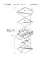
- FIG. 1is an exploded perspective view of an electronic circuit and shielding and thermal dissipation structure embodying the present invention
- FIG. 2is a cross-sectional view taken along line 2 — 2 of FIG. 1;
- FIG. 3is an enlarged cross sectional view of a portion of FIG. 2;
- FIG. 4is a cross-sectional view similar to FIG. 2 but illustrating an alternative embodiment of the present invention.
- FIGS. 1-3illustrate a preferred embodiment of the present invention as usable with an electronic assembly such as might be usable in virtually any electronic device, but which can be particularly advantageously used with portable electronic assemblies such as cellular telephones.
- a printed circuit board (PCB) 10is provided to suitably interconnect suitable microcircuitry chips 12 , 14 , such as Flip Chips or chip scale packages (CSP). As illustrated in FIG. 2, the chips 12 , 14 are suitably connected to the PCB 10 , as by the discrete mechanical connections 16 shown in the form of solder balls.
- PCBprinted circuit board
- a plastic housing 20is provided, and has an outer periphery 22 which is closed on one side (defined by top wall 24 shown in FIGS. 2 and 3) and open on the other side of the periphery 22 (the bottom side in the Figures) which faces the PCB 10 and chips 12 , 14 .
- this plastic housing 20can be can be relatively thin (for example, 0.05 mm thick) and made of plastic such as polyetherimide or other suitable plastics which can withstand 125 degree C. operating temperatures without permanent deformation.
- the plastic housing 20is metalized on its interior surface, preferably with Nickel or Gold, in sufficient thickness for shielding the circuitry.
- This metal coating or metalized plating 28is shown in FIG. 3 and, for applications such as cellular telephones, should preferably be at least about 5 microns thick, although greater thicknesses could, of course, be used.
- Coatings with silver particles in a polymer matrixare preferably 10-20 microns thick.
- an electrically conductive gel 30Molded within the interior of the housing 20 around its outer periphery 22 (that is, in a peripheral interior region) is an electrically conductive gel 30 .
- the gel 30is in intimate contact with a metalized pattern on the PCB 20 , for example through a solder ball 32 between the two.
- the gel 30may be a silicone elastomer filled with suitable materials to enhance its electrical conductivity.
- carbon particles or carbon fibers or a combination of bothcan be included in a silicone elastomer gel to provide an environmentally stable contact with the metalized plating 28 on the inner surface of the housing 20 . This thus provides an excellent EMI and RF shielding for the chips 12 , 14 contained in the housing interior as further described below.
- thermally conductive gel 40molded within the interior of the housing 20 inside of the electrically conductive gel 30 (that is, in a central interior region surrounded by the peripheral outer region) is a thermally conductive gel 40 .
- the thermally conductive gel 40is cast to form negative cavities 42 matching the placement of components such as chips 12 , 14 on the PCB 10 .
- the thermally conductive gel 40may also be a silicone elastomer, but filled with suitable materials to enhance its thermal conductivity.
- suitable materialsfor example, particles of alumina (aluminum oxide), aluminum nitride, or boron nitride or combinations thereof may be included in the gel 40 to provide low electrical conductivity and a dielectric constant value so as to not effect circuit performance (due to its intimate contact with the chips 12 , 14 and PCB 10 ) while also providing good thermal conductivity, taking heat away from the PCB 10 and chips 12 , 14 and to the housing 20 (and particularly its top wall 24 ) to prevent overheating of the circuitry.
- the gel 40adheres to the chips 12 , 14 and PCB 10 by surface tension, thereby allowing the a reliable contact to be maintained without high clamping forces.
- Thisalso allows clamping of the components together without secondary fasteners, as simple snap together plastic housing connectors can be used.
- This structureavoids the assembly problems associated with some prior art as noted above in the Background.
- This surface tension contactis also sufficient to exclude moisture and dust and other environmental contaminants under most operating conditions as might be expected, for example, with cellular telephones.
- Use of a thermally conductive gel such as aboveis also described in U.S. patent appl. Ser. No. 08/995,388, filed Dec. 22, 1997 by James D. MacDonald, Jr., Walter M. Marcinkiewicz and Rahul Gupta, and entitled “Shock and Vibration Attenuating Structure for an Electronic Assembly”, and that complete contents of that application are hereby incorporated by reference.
- a second layer of thermally conductive gel 50may also be provided on the exterior surface of the plastic housing 20 and extending to an outer housing 52 of the device (for example, the exterior housing of a cellular telephone) to further assist in thermal dissipation.
- This structurethus allows leeway in manufacturing tolerances when assembling the device, in addition to allowing significant flexure of the outer housing 52 during use without breaking contact of the gel 40 with the PCB 10 .
- the device housingitself as the plastic housing, with the interior of the device housing metalized and the interior thermally conductive gel 40 directly contacting the metalized interior surface of the device housing.
- FIG. 4illustrates an alternative embodiment of the present invention. Identical components to those in the first described embodiment are given the same reference numbers and similar but modified components are given the same reference numbers with prime “′” added.
- an additional wall 60is formed with the plastic housing 20 ′ so as to separate the peripheral and central interior regions.
- This additional wall 60can be used to facilitate molding of the gels 30 ′, 40 ′, which would then be separated rather than in direct contact. It should be appreciated, however, that with such a structure the metalized plating (not shown on FIG. 4) would necessarily extend around the wall 60 or some other electrical contact would be required in order to maintain an electrical contact between the surface of the housing 20 ′ contacted by the electrically conductive gel 30 ′ with the metalized plating on the interior surface of the top wall 24 .
- the present inventionmay be easily, inexpensively, and reliable assembled in a wide variety of devices. Still further, it should be appreciated that this invention will provide a simple and reliable structure providing EMI/RF shielding, thermal control, and shock/vibration attenuation, as well as protecting the electronic components from environmental contaminants such as moisture and dust.
Landscapes
- Engineering & Computer Science (AREA)
- Microelectronics & Electronic Packaging (AREA)
- Physics & Mathematics (AREA)
- Power Engineering (AREA)
- Condensed Matter Physics & Semiconductors (AREA)
- General Physics & Mathematics (AREA)
- Computer Hardware Design (AREA)
- Toxicology (AREA)
- Electromagnetism (AREA)
- Health & Medical Sciences (AREA)
- Shielding Devices Or Components To Electric Or Magnetic Fields (AREA)
- Structures Or Materials For Encapsulating Or Coating Semiconductor Devices Or Solid State Devices (AREA)
- Cooling Or The Like Of Electrical Apparatus (AREA)
Abstract
Description
Claims (22)
Priority Applications (7)
| Application Number | Priority Date | Filing Date | Title |
|---|---|---|---|
| US09/338,818US6195267B1 (en) | 1999-06-23 | 1999-06-23 | Gel structure for combined EMI shielding and thermal control of microelectronic assemblies |
| CNB008094837ACN1189069C (en) | 1999-06-23 | 2000-06-05 | A shield and heat sink for a microelectronic assembly |
| JP2001504738AJP2003502853A (en) | 1999-06-23 | 2000-06-05 | Gel structures for combined EMI shielding and thermal control of microelectronic assemblies |
| PCT/US2000/015398WO2000079856A1 (en) | 1999-06-23 | 2000-06-05 | Gel structure for combined emi shielding and thermal control of microelectronic assemblies |
| AU54635/00AAU5463500A (en) | 1999-06-23 | 2000-06-05 | Gel structure for combined emi shielding and thermal control of microelectronic assemblies |
| DE10084732TDE10084732T1 (en) | 1999-06-23 | 2000-06-05 | Gel structure for combined EMI shielding and thermal control of microelectronic devices |
| MYPI20002635MY126725A (en) | 1999-06-23 | 2000-06-12 | Gel structure for combined emi shielding and thermal control of microelectronic assemblies |
Applications Claiming Priority (1)
| Application Number | Priority Date | Filing Date | Title |
|---|---|---|---|
| US09/338,818US6195267B1 (en) | 1999-06-23 | 1999-06-23 | Gel structure for combined EMI shielding and thermal control of microelectronic assemblies |
Publications (1)
| Publication Number | Publication Date |
|---|---|
| US6195267B1true US6195267B1 (en) | 2001-02-27 |
Family
ID=23326294
Family Applications (1)
| Application Number | Title | Priority Date | Filing Date |
|---|---|---|---|
| US09/338,818Expired - LifetimeUS6195267B1 (en) | 1999-06-23 | 1999-06-23 | Gel structure for combined EMI shielding and thermal control of microelectronic assemblies |
Country Status (7)
| Country | Link |
|---|---|
| US (1) | US6195267B1 (en) |
| JP (1) | JP2003502853A (en) |
| CN (1) | CN1189069C (en) |
| AU (1) | AU5463500A (en) |
| DE (1) | DE10084732T1 (en) |
| MY (1) | MY126725A (en) |
| WO (1) | WO2000079856A1 (en) |
Cited By (95)
| Publication number | Priority date | Publication date | Assignee | Title |
|---|---|---|---|---|
| US6472598B1 (en)* | 1998-08-28 | 2002-10-29 | Amkor Technology, Inc. | Electromagnetic interference shield device with conductive encapsulant and dam |
| US6487073B2 (en)* | 1999-12-01 | 2002-11-26 | Cool Options, Inc. | Thermally conductive electronic device case |
| US6498733B2 (en)* | 2000-03-03 | 2002-12-24 | Sony Computer Entertainment Inc. | Electronic device and shield |
| US20030066672A1 (en)* | 2001-05-10 | 2003-04-10 | Watchko George R. | Thermal-sprayed metallic conformal coatings used as heat spreaders |
| US6614102B1 (en) | 2001-05-04 | 2003-09-02 | Amkor Technology, Inc. | Shielded semiconductor leadframe package |
| US6624432B1 (en)* | 1999-10-12 | 2003-09-23 | Shielding For Electronics, Inc. | EMI containment apparatus |
| WO2003088729A1 (en)* | 2002-04-10 | 2003-10-23 | Gore Enterprise Holdings, Inc. | Board-level emi shield with enhanced thermal dissipation |
| US20030222249A1 (en)* | 2002-05-31 | 2003-12-04 | Bunyan Michael H. | Thermally or electrically-conductive form-in-place gap filter |
| US20040014508A1 (en)* | 2002-06-24 | 2004-01-22 | Seo Dong Han | Apparatus for improving reception sensitivity of public wave receiver |
| US20040020673A1 (en)* | 2001-03-19 | 2004-02-05 | Mazurkiewicz Paul H. | Board-level conformal EMI shield having an electrically-conductive polymer coating over a thermally-conductive dielectric coating |
| US20050052858A1 (en)* | 2003-09-05 | 2005-03-10 | Nec Corporation | Compact radio equipment and method of mounting the same |
| US20050095410A1 (en)* | 2001-03-19 | 2005-05-05 | Mazurkiewicz Paul H. | Board-level conformal EMI shield having an electrically-conductive polymer coating over a thermally-conductive dielectric coating |
| US20050111194A1 (en)* | 2003-11-21 | 2005-05-26 | Lg Electronics Inc. | Heat radiating system and method for a mobile communication terminal |
| US20050161253A1 (en)* | 2004-01-23 | 2005-07-28 | Pitney Bowes Incorporated | Tamper barrier for electronic device |
| US20050222657A1 (en)* | 2004-03-30 | 2005-10-06 | Wahlstrand Carl D | MRI-safe implantable lead |
| US20050222656A1 (en)* | 2004-03-30 | 2005-10-06 | Wahlstrand Carl D | MRI-safe implantable medical device |
| US20050222658A1 (en)* | 2004-03-30 | 2005-10-06 | Medtronic, Inc. | Lead electrode for use in an MRI-safe implantable medical device |
| US20050222659A1 (en)* | 2004-03-30 | 2005-10-06 | Medtronic, Inc. | Lead electrode for use in an MRI-safe implantable medical device |
| US20050276424A1 (en)* | 2004-05-27 | 2005-12-15 | Shaver Charles N | Computer speaker beep routing |
| US20050274630A1 (en)* | 2004-06-15 | 2005-12-15 | Pitney Bowes Incorporated | Tamper barrier enclosure with corner protection |
| US20060021903A1 (en)* | 2004-01-23 | 2006-02-02 | Perreault Paul G | System and method for installing a tamper barrier wrap in a PCB assembly, including a PCB assembly having improved heat sinking |
| US20060047053A1 (en)* | 2004-08-27 | 2006-03-02 | Ivan Pawlenko | Thermoconductive composition for RF shielding |
| US20060086518A1 (en)* | 2003-03-31 | 2006-04-27 | Toshiyuki Kawaguchi | Shield box and shield method |
| US20060109639A1 (en)* | 2004-11-22 | 2006-05-25 | Nec Corporation | Electronic apparatus |
| US20060200218A1 (en)* | 2005-02-01 | 2006-09-07 | Wahlstrand Carl D | Extensible implantable medical lead |
| US20060247748A1 (en)* | 2005-04-29 | 2006-11-02 | Medtronic, Inc. | Lead electrode for use in an MRI-safe implantable medical device |
| US20070137836A1 (en)* | 2005-12-19 | 2007-06-21 | Qnx Cooling Systems, Inc. | Heat transfer system |
| US7262369B1 (en) | 2006-03-09 | 2007-08-28 | Laird Technologies, Inc. | Combined board level EMI shielding and thermal management |
| US20070211436A1 (en)* | 2006-03-09 | 2007-09-13 | Robinson Kenneth M | Combined board level shielding and thermal management |
| US20070210082A1 (en)* | 2006-03-09 | 2007-09-13 | English Gerald R | EMI shielding and thermal management assemblies including frames and covers with multi-position latching |
| US20070211445A1 (en)* | 2006-03-09 | 2007-09-13 | Robinson Kenneth M | Low-profile board level EMI shielding and thermal management apparatus and spring clips for use therewith |
| US20080080160A1 (en)* | 2005-12-16 | 2008-04-03 | Laird Technologies, Inc. | Emi shielding assemblies |
| US20080106884A1 (en)* | 2006-11-03 | 2008-05-08 | Gerald Robert English | Snap install emi shields with protrusions and electrically-conductive members for attachment to substrates |
| US20080195186A1 (en)* | 2007-02-14 | 2008-08-14 | Bernard Li | Continuous conductive materials for electromagnetic shielding |
| US20080195187A1 (en)* | 2007-02-14 | 2008-08-14 | Bernard Li | Discontinuous conductive filler polymer-matrix composites for electromagnetic shielding |
| US20080269863A1 (en)* | 2007-04-25 | 2008-10-30 | Medtronic, Inc. | Lead or lead extension having a conductive body and conductive body contact |
| US20090086890A1 (en)* | 2007-09-28 | 2009-04-02 | Fujifilm Corporation | Radiation image capturing apparatus |
| US20090207578A1 (en)* | 2008-02-20 | 2009-08-20 | Chris Ligtenberg | Apparatus for reducing electromagnetic interference and spreading heat |
| US20100008047A1 (en)* | 2005-11-07 | 2010-01-14 | Moon Sung-Won | Passive thermal solution for hand-held devices |
| US7853332B2 (en) | 2005-04-29 | 2010-12-14 | Medtronic, Inc. | Lead electrode for use in an MRI-safe implantable medical device |
| US20110026229A1 (en)* | 2009-01-20 | 2011-02-03 | Wei-Kai Hsiao | Electronic device having cushioning member |
| US20110032692A1 (en)* | 2008-04-17 | 2011-02-10 | Laird Technologies, Inc. | Emi shielding slide assemblies for slidably opening and closing portable electronic devices and for providing emi shielding for board-mounted electronic components |
| US7965514B2 (en) | 2009-06-05 | 2011-06-21 | Laird Technologies, Inc. | Assemblies and methods for dissipating heat from handheld electronic devices |
| US20120051006A1 (en)* | 2010-08-27 | 2012-03-01 | Gm Global Technology Operations, Inc | Mounted circuit card assembly |
| WO2012076232A1 (en)* | 2010-12-08 | 2012-06-14 | Robert Bosch Gmbh | Control module and method for producing same |
| US20120240396A1 (en)* | 2007-06-28 | 2012-09-27 | Rolf Becker | use of a control module for a transmission control installed in an automatic transmission |
| US20130050950A1 (en)* | 2011-08-31 | 2013-02-28 | Apple Inc. | Systems and method for providing a graphite layer in an electronic device |
| US8477499B2 (en) | 2009-06-05 | 2013-07-02 | Laird Technologies, Inc. | Assemblies and methods for dissipating heat from handheld electronic devices |
| US20140002996A1 (en)* | 2012-06-28 | 2014-01-02 | Shayan Malek | Thermally Conductive Printed Circuit Board Bumpers |
| US8989840B2 (en) | 2004-03-30 | 2015-03-24 | Medtronic, Inc. | Lead electrode for use in an MRI-safe implantable medical device |
| US20150319886A1 (en)* | 2010-10-26 | 2015-11-05 | Tdk-Lambda Corporation | Thermal Management System and Method |
| US9186499B2 (en) | 2009-04-30 | 2015-11-17 | Medtronic, Inc. | Grounding of a shield within an implantable medical lead |
| US9463317B2 (en) | 2012-04-19 | 2016-10-11 | Medtronic, Inc. | Paired medical lead bodies with braided conductive shields having different physical parameter values |
| US20160353616A1 (en)* | 2010-04-19 | 2016-12-01 | Apple Inc. | Electronic subassemblies for electronic devices |
| US9520645B2 (en) | 2013-09-09 | 2016-12-13 | Apple Inc. | Electronic device with electromagnetic shielding structures |
| US9554477B1 (en) | 2015-12-18 | 2017-01-24 | International Business Machines Corporation | Tamper-respondent assemblies with enclosure-to-board protection |
| US9560737B2 (en) | 2015-03-04 | 2017-01-31 | International Business Machines Corporation | Electronic package with heat transfer element(s) |
| US9555606B1 (en) | 2015-12-09 | 2017-01-31 | International Business Machines Corporation | Applying pressure to adhesive using CTE mismatch between components |
| US9578764B1 (en) | 2015-09-25 | 2017-02-21 | International Business Machines Corporation | Enclosure with inner tamper-respondent sensor(s) and physical security element(s) |
| US9591776B1 (en) | 2015-09-25 | 2017-03-07 | International Business Machines Corporation | Enclosure with inner tamper-respondent sensor(s) |
| US9731119B2 (en) | 2008-03-12 | 2017-08-15 | Medtronic, Inc. | System and method for implantable medical device lead shielding |
| US20170295641A1 (en)* | 2016-04-07 | 2017-10-12 | Azbil Corporation | Substrate unit and method of manufacturing substrate unit |
| US9858776B1 (en) | 2016-06-28 | 2018-01-02 | International Business Machines Corporation | Tamper-respondent assembly with nonlinearity monitoring |
| US9881880B2 (en) | 2016-05-13 | 2018-01-30 | International Business Machines Corporation | Tamper-proof electronic packages with stressed glass component substrate(s) |
| US9894749B2 (en) | 2015-09-25 | 2018-02-13 | International Business Machines Corporation | Tamper-respondent assemblies with bond protection |
| US9904811B2 (en) | 2016-04-27 | 2018-02-27 | International Business Machines Corporation | Tamper-proof electronic packages with two-phase dielectric fluid |
| US9911012B2 (en) | 2015-09-25 | 2018-03-06 | International Business Machines Corporation | Overlapping, discrete tamper-respondent sensors |
| US9913370B2 (en) | 2016-05-13 | 2018-03-06 | International Business Machines Corporation | Tamper-proof electronic packages formed with stressed glass |
| US9913389B2 (en) | 2015-12-01 | 2018-03-06 | International Business Corporation Corporation | Tamper-respondent assembly with vent structure |
| US9916744B2 (en) | 2016-02-25 | 2018-03-13 | International Business Machines Corporation | Multi-layer stack with embedded tamper-detect protection |
| US9924591B2 (en) | 2015-09-25 | 2018-03-20 | International Business Machines Corporation | Tamper-respondent assemblies |
| US9978231B2 (en) | 2015-10-21 | 2018-05-22 | International Business Machines Corporation | Tamper-respondent assembly with protective wrap(s) over tamper-respondent sensor(s) |
| US9993638B2 (en) | 2013-12-14 | 2018-06-12 | Medtronic, Inc. | Devices, systems and methods to reduce coupling of a shield and a conductor within an implantable medical lead |
| US9999124B2 (en) | 2016-11-02 | 2018-06-12 | International Business Machines Corporation | Tamper-respondent assemblies with trace regions of increased susceptibility to breaking |
| US10098235B2 (en) | 2015-09-25 | 2018-10-09 | International Business Machines Corporation | Tamper-respondent assemblies with region(s) of increased susceptibility to damage |
| US10136519B2 (en) | 2015-10-19 | 2018-11-20 | International Business Machines Corporation | Circuit layouts of tamper-respondent sensors |
| US10155111B2 (en) | 2014-07-24 | 2018-12-18 | Medtronic, Inc. | Methods of shielding implantable medical leads and implantable medical lead extensions |
| US10172239B2 (en) | 2015-09-25 | 2019-01-01 | International Business Machines Corporation | Tamper-respondent sensors with formed flexible layer(s) |
| US10168185B2 (en) | 2015-09-25 | 2019-01-01 | International Business Machines Corporation | Circuit boards and electronic packages with embedded tamper-respondent sensor |
| US10271424B2 (en) | 2016-09-26 | 2019-04-23 | International Business Machines Corporation | Tamper-respondent assemblies with in situ vent structure(s) |
| US10279171B2 (en) | 2014-07-23 | 2019-05-07 | Medtronic, Inc. | Methods of shielding implantable medical leads and implantable medical lead extensions |
| US10299372B2 (en) | 2016-09-26 | 2019-05-21 | International Business Machines Corporation | Vented tamper-respondent assemblies |
| CN109804264A (en)* | 2016-10-13 | 2019-05-24 | 黑拉有限责任两合公司 | Radar installations with shielding device |
| US10306753B1 (en) | 2018-02-22 | 2019-05-28 | International Business Machines Corporation | Enclosure-to-board interface with tamper-detect circuit(s) |
| US10321589B2 (en) | 2016-09-19 | 2019-06-11 | International Business Machines Corporation | Tamper-respondent assembly with sensor connection adapter |
| US10327343B2 (en) | 2015-12-09 | 2019-06-18 | International Business Machines Corporation | Applying pressure to adhesive using CTE mismatch between components |
| US10327329B2 (en) | 2017-02-13 | 2019-06-18 | International Business Machines Corporation | Tamper-respondent assembly with flexible tamper-detect sensor(s) overlying in-situ-formed tamper-detect sensor |
| US10359812B2 (en)* | 2017-12-12 | 2019-07-23 | Motorola Mobility Llc | Device component exposure protection |
| US10426037B2 (en) | 2015-07-15 | 2019-09-24 | International Business Machines Corporation | Circuitized structure with 3-dimensional configuration |
| CN111837052A (en)* | 2018-03-13 | 2020-10-27 | 海拉有限双合股份公司 | Radar device, in particular for a motor vehicle |
| US10825781B2 (en) | 2018-08-01 | 2020-11-03 | Nxp B.V. | Semiconductor device with conductive film shielding |
| US11122682B2 (en) | 2018-04-04 | 2021-09-14 | International Business Machines Corporation | Tamper-respondent sensors with liquid crystal polymer layers |
| US11172567B2 (en) | 2017-09-13 | 2021-11-09 | Xi'an Zhongxing New Software Co., Ltd. | Assembly method and device for circuit structural member and circuit structural member |
| CN116669279A (en)* | 2022-12-30 | 2023-08-29 | 荣耀终端有限公司 | Circuit board assembly and electronic equipment |
| US12218018B2 (en) | 2022-04-21 | 2025-02-04 | Infineon Technologies Ag | Semiconductor encapsulant strength enhancer |
Families Citing this family (12)
| Publication number | Priority date | Publication date | Assignee | Title |
|---|---|---|---|---|
| ES2290062T3 (en)* | 1999-12-01 | 2008-02-16 | Cool Options, Inc. | STRUCTURAL TABLE OF THERMOCONDUCTIVE MATERIALS. |
| BRPI0100051B1 (en) | 2001-01-11 | 2016-11-29 | Brasil Compressores Sa | electronic device enclosure |
| DE60222815T2 (en)* | 2001-04-03 | 2008-07-03 | AUTONETWORKS Technologies, LTD., Yokkaichi | Optical connector, optical element mounting device, and optical connector mounting part |
| JP2005051129A (en)* | 2003-07-30 | 2005-02-24 | Sony Corp | Electronic apparatus |
| CN100405587C (en)* | 2003-11-22 | 2008-07-23 | 鸿富锦精密工业(深圳)有限公司 | Radiator and its preparation method |
| US7492594B2 (en)* | 2007-05-03 | 2009-02-17 | Hamilton Sundstrand Corporation | Electronic circuit modules cooling |
| JP5698894B2 (en)* | 2008-10-24 | 2015-04-08 | 三菱電機株式会社 | Heat dissipation structure for electronic components |
| JP5512566B2 (en)* | 2011-01-31 | 2014-06-04 | 株式会社東芝 | Semiconductor device |
| CN104302160A (en)* | 2014-10-14 | 2015-01-21 | 江西清华泰豪微电机有限公司 | Shielding device of voltage adjuster |
| KR102286337B1 (en)* | 2014-10-17 | 2021-08-04 | 쓰리엠 이노베이티브 프로퍼티즈 컴파니 | Emi shielding structure and thermal pad, and electronic circuit board assembly including the same |
| DE102018215338B3 (en)* | 2018-09-10 | 2020-01-16 | Dürkopp Adler AG | Cooling device for at least one component mounted on a printed circuit board |
| CN111123291B (en)* | 2020-03-31 | 2020-06-30 | 深圳市汇顶科技股份有限公司 | Time-of-flight emission module, time-of-flight detection device and electronic equipment |
Citations (8)
| Publication number | Priority date | Publication date | Assignee | Title |
|---|---|---|---|---|
| US4008300A (en) | 1974-10-15 | 1977-02-15 | A & P Products Incorporated | Multi-conductor element and method of making same |
| US4770641A (en) | 1986-03-31 | 1988-09-13 | Amp Incorporated | Conductive gel interconnection apparatus |
| US4855868A (en)* | 1987-01-20 | 1989-08-08 | Harding Ade Yemi S K | Preformed packaging arrangement for energy dissipating devices |
| US5074799A (en) | 1991-03-27 | 1991-12-24 | Amp Incorporated | Gel connector of laminar construction |
| US5294826A (en)* | 1993-04-16 | 1994-03-15 | Northern Telecom Limited | Integrated circuit package and assembly thereof for thermal and EMI management |
| US5424652A (en) | 1992-06-10 | 1995-06-13 | Micron Technology, Inc. | Method and apparatus for testing an unpackaged semiconductor die |
| US5561265A (en)* | 1993-03-24 | 1996-10-01 | Northern Telecom Limited | Integrated circuit packaging |
| US6090728A (en)* | 1998-05-01 | 2000-07-18 | 3M Innovative Properties Company | EMI shielding enclosures |
Family Cites Families (13)
| Publication number | Priority date | Publication date | Assignee | Title |
|---|---|---|---|---|
| US3616533A (en)* | 1969-10-28 | 1971-11-02 | North American Rockwell | Method of protecting articles in high temperature environment |
| US4768286A (en)* | 1986-10-01 | 1988-09-06 | Eastman Christensen Co. | Printed circuit packaging for high vibration and temperature environments |
| JPH0567893A (en)* | 1991-09-10 | 1993-03-19 | Mitsubishi Electric Corp | Local shielding method for circuit board |
| JPH05235023A (en)* | 1992-02-26 | 1993-09-10 | Matsushita Electron Corp | Semiconductor device and manufacture thereof |
| JP2586389B2 (en)* | 1993-09-17 | 1997-02-26 | 日本電気株式会社 | LSI case shield structure |
| JPH07111299A (en)* | 1993-10-14 | 1995-04-25 | Fuji Xerox Co Ltd | Hybrid integrated circuit |
| JPH0832272A (en)* | 1994-07-20 | 1996-02-02 | Nec Eng Ltd | Shield structure |
| JPH0961456A (en)* | 1995-08-29 | 1997-03-07 | Murata Mfg Co Ltd | Semiconductor device |
| DE29514398U1 (en)* | 1995-09-07 | 1995-10-19 | Siemens AG, 80333 München | Shielding for printed circuit boards |
| JPH1041678A (en)* | 1996-07-25 | 1998-02-13 | Hitachi Ltd | Optical receiver |
| JP3082905B2 (en)* | 1997-01-28 | 2000-09-04 | 富士通電装株式会社 | Chip-on-board shielding structure and method of manufacturing the same |
| SE511926C2 (en)* | 1997-04-16 | 1999-12-20 | Ericsson Telefon Ab L M | Screen enclosure as well as process for making and using a screen enclosure and mobile phone with screen enclosure |
| US5867371A (en)* | 1997-09-29 | 1999-02-02 | Ericsson Inc. | Cover member for sealed circuit board assembly |
- 1999
- 1999-06-23USUS09/338,818patent/US6195267B1/ennot_activeExpired - Lifetime
- 2000
- 2000-06-05CNCNB008094837Apatent/CN1189069C/ennot_activeExpired - Fee Related
- 2000-06-05JPJP2001504738Apatent/JP2003502853A/ennot_activeCeased
- 2000-06-05WOPCT/US2000/015398patent/WO2000079856A1/enactiveApplication Filing
- 2000-06-05DEDE10084732Tpatent/DE10084732T1/ennot_activeWithdrawn
- 2000-06-05AUAU54635/00Apatent/AU5463500A/ennot_activeAbandoned
- 2000-06-12MYMYPI20002635patent/MY126725A/enunknown
Patent Citations (8)
| Publication number | Priority date | Publication date | Assignee | Title |
|---|---|---|---|---|
| US4008300A (en) | 1974-10-15 | 1977-02-15 | A & P Products Incorporated | Multi-conductor element and method of making same |
| US4770641A (en) | 1986-03-31 | 1988-09-13 | Amp Incorporated | Conductive gel interconnection apparatus |
| US4855868A (en)* | 1987-01-20 | 1989-08-08 | Harding Ade Yemi S K | Preformed packaging arrangement for energy dissipating devices |
| US5074799A (en) | 1991-03-27 | 1991-12-24 | Amp Incorporated | Gel connector of laminar construction |
| US5424652A (en) | 1992-06-10 | 1995-06-13 | Micron Technology, Inc. | Method and apparatus for testing an unpackaged semiconductor die |
| US5561265A (en)* | 1993-03-24 | 1996-10-01 | Northern Telecom Limited | Integrated circuit packaging |
| US5294826A (en)* | 1993-04-16 | 1994-03-15 | Northern Telecom Limited | Integrated circuit package and assembly thereof for thermal and EMI management |
| US6090728A (en)* | 1998-05-01 | 2000-07-18 | 3M Innovative Properties Company | EMI shielding enclosures |
Cited By (187)
| Publication number | Priority date | Publication date | Assignee | Title |
|---|---|---|---|---|
| US6472598B1 (en)* | 1998-08-28 | 2002-10-29 | Amkor Technology, Inc. | Electromagnetic interference shield device with conductive encapsulant and dam |
| US6601293B1 (en) | 1998-08-28 | 2003-08-05 | Amkor Technology, Inc. | Method of making an electromagnetic interference shield device |
| US6624432B1 (en)* | 1999-10-12 | 2003-09-23 | Shielding For Electronics, Inc. | EMI containment apparatus |
| US6487073B2 (en)* | 1999-12-01 | 2002-11-26 | Cool Options, Inc. | Thermally conductive electronic device case |
| US6498733B2 (en)* | 2000-03-03 | 2002-12-24 | Sony Computer Entertainment Inc. | Electronic device and shield |
| US20040020673A1 (en)* | 2001-03-19 | 2004-02-05 | Mazurkiewicz Paul H. | Board-level conformal EMI shield having an electrically-conductive polymer coating over a thermally-conductive dielectric coating |
| US7214889B2 (en)* | 2001-03-19 | 2007-05-08 | Hewlett-Packard Development Company, L.P. | Board-level conformal EMI shield having an electrically-conductive polymer coating over a thermally-conductive dielectric coating |
| US20050095410A1 (en)* | 2001-03-19 | 2005-05-05 | Mazurkiewicz Paul H. | Board-level conformal EMI shield having an electrically-conductive polymer coating over a thermally-conductive dielectric coating |
| US6614102B1 (en) | 2001-05-04 | 2003-09-02 | Amkor Technology, Inc. | Shielded semiconductor leadframe package |
| US6965071B2 (en) | 2001-05-10 | 2005-11-15 | Parker-Hannifin Corporation | Thermal-sprayed metallic conformal coatings used as heat spreaders |
| US20030066672A1 (en)* | 2001-05-10 | 2003-04-10 | Watchko George R. | Thermal-sprayed metallic conformal coatings used as heat spreaders |
| US6744640B2 (en) | 2002-04-10 | 2004-06-01 | Gore Enterprise Holdings, Inc. | Board-level EMI shield with enhanced thermal dissipation |
| WO2003088729A1 (en)* | 2002-04-10 | 2003-10-23 | Gore Enterprise Holdings, Inc. | Board-level emi shield with enhanced thermal dissipation |
| CN100438737C (en)* | 2002-04-10 | 2008-11-26 | 戈尔企业控股股份有限公司 | Board-level EMI shielding with enhanced heat dissipation |
| WO2003103044A1 (en)* | 2002-05-31 | 2003-12-11 | Parker Hannifin Corporation | Thermally or electrically conductive gap filler |
| US20030222249A1 (en)* | 2002-05-31 | 2003-12-04 | Bunyan Michael H. | Thermally or electrically-conductive form-in-place gap filter |
| US7208192B2 (en) | 2002-05-31 | 2007-04-24 | Parker-Hannifin Corporation | Thermally or electrically-conductive form-in-place gap filter |
| US20040014508A1 (en)* | 2002-06-24 | 2004-01-22 | Seo Dong Han | Apparatus for improving reception sensitivity of public wave receiver |
| US7245896B2 (en)* | 2002-06-24 | 2007-07-17 | Lg Electronics Inc. | Apparatus for improving reception sensitivity of public wave receiver by reducing noise externally-emitted in the public wave receiver |
| WO2004043123A1 (en)* | 2002-11-01 | 2004-05-21 | Parker-Hannifin Corporation | Thermal-sprayed metallic conformal coatings used as heat spreaders |
| US20060086518A1 (en)* | 2003-03-31 | 2006-04-27 | Toshiyuki Kawaguchi | Shield box and shield method |
| US20050052858A1 (en)* | 2003-09-05 | 2005-03-10 | Nec Corporation | Compact radio equipment and method of mounting the same |
| US7177161B2 (en)* | 2003-09-05 | 2007-02-13 | Seiko Epson Corporation | Compact radio equipment and method of mounting the same |
| US20070059981A1 (en)* | 2003-09-05 | 2007-03-15 | Nec Corporation | Compact radio equipment and method of mounting the same |
| US7286360B2 (en)* | 2003-11-21 | 2007-10-23 | Lg Electronics Inc. | Heat radiating system and method for a mobile communication terminal |
| US20050111194A1 (en)* | 2003-11-21 | 2005-05-26 | Lg Electronics Inc. | Heat radiating system and method for a mobile communication terminal |
| US7475474B2 (en) | 2004-01-23 | 2009-01-13 | Pitney Bowes Inc. | Method of making tamper detection circuit for an electronic device |
| US20050161253A1 (en)* | 2004-01-23 | 2005-07-28 | Pitney Bowes Incorporated | Tamper barrier for electronic device |
| US20060021903A1 (en)* | 2004-01-23 | 2006-02-02 | Perreault Paul G | System and method for installing a tamper barrier wrap in a PCB assembly, including a PCB assembly having improved heat sinking |
| US7180008B2 (en) | 2004-01-23 | 2007-02-20 | Pitney Bowes Inc. | Tamper barrier for electronic device |
| US7877150B2 (en) | 2004-03-30 | 2011-01-25 | Medtronic, Inc. | Lead electrode for use in an MRI-safe implantable medical device |
| US9302101B2 (en) | 2004-03-30 | 2016-04-05 | Medtronic, Inc. | MRI-safe implantable lead |
| US7844343B2 (en) | 2004-03-30 | 2010-11-30 | Medtronic, Inc. | MRI-safe implantable medical device |
| US20050222659A1 (en)* | 2004-03-30 | 2005-10-06 | Medtronic, Inc. | Lead electrode for use in an MRI-safe implantable medical device |
| US8989840B2 (en) | 2004-03-30 | 2015-03-24 | Medtronic, Inc. | Lead electrode for use in an MRI-safe implantable medical device |
| US20050222658A1 (en)* | 2004-03-30 | 2005-10-06 | Medtronic, Inc. | Lead electrode for use in an MRI-safe implantable medical device |
| US20050222657A1 (en)* | 2004-03-30 | 2005-10-06 | Wahlstrand Carl D | MRI-safe implantable lead |
| US20050222656A1 (en)* | 2004-03-30 | 2005-10-06 | Wahlstrand Carl D | MRI-safe implantable medical device |
| US9155877B2 (en) | 2004-03-30 | 2015-10-13 | Medtronic, Inc. | Lead electrode for use in an MRI-safe implantable medical device |
| US7844344B2 (en)* | 2004-03-30 | 2010-11-30 | Medtronic, Inc. | MRI-safe implantable lead |
| US20050276424A1 (en)* | 2004-05-27 | 2005-12-15 | Shaver Charles N | Computer speaker beep routing |
| US20050274630A1 (en)* | 2004-06-15 | 2005-12-15 | Pitney Bowes Incorporated | Tamper barrier enclosure with corner protection |
| US7156233B2 (en) | 2004-06-15 | 2007-01-02 | Pitney Bowes Inc. | Tamper barrier enclosure with corner protection |
| US20060047053A1 (en)* | 2004-08-27 | 2006-03-02 | Ivan Pawlenko | Thermoconductive composition for RF shielding |
| US20100116431A1 (en)* | 2004-08-27 | 2010-05-13 | Ivan Pawlenko | Thermoconductive composition for rf shielding |
| US20060109639A1 (en)* | 2004-11-22 | 2006-05-25 | Nec Corporation | Electronic apparatus |
| US20060200218A1 (en)* | 2005-02-01 | 2006-09-07 | Wahlstrand Carl D | Extensible implantable medical lead |
| US8280526B2 (en) | 2005-02-01 | 2012-10-02 | Medtronic, Inc. | Extensible implantable medical lead |
| US7853332B2 (en) | 2005-04-29 | 2010-12-14 | Medtronic, Inc. | Lead electrode for use in an MRI-safe implantable medical device |
| US8027736B2 (en) | 2005-04-29 | 2011-09-27 | Medtronic, Inc. | Lead electrode for use in an MRI-safe implantable medical device |
| US9265940B2 (en)* | 2005-04-29 | 2016-02-23 | Medtronic, Inc. | Lead electrode for use in an MRI-safe implantable medical device |
| US20150039064A1 (en)* | 2005-04-29 | 2015-02-05 | Medtronic, Inc. | Lead electrode for use in an mri-safe implantable medical device |
| US20060247748A1 (en)* | 2005-04-29 | 2006-11-02 | Medtronic, Inc. | Lead electrode for use in an MRI-safe implantable medical device |
| US20100008047A1 (en)* | 2005-11-07 | 2010-01-14 | Moon Sung-Won | Passive thermal solution for hand-held devices |
| US20080080160A1 (en)* | 2005-12-16 | 2008-04-03 | Laird Technologies, Inc. | Emi shielding assemblies |
| US20070137836A1 (en)* | 2005-12-19 | 2007-06-21 | Qnx Cooling Systems, Inc. | Heat transfer system |
| US7623360B2 (en)* | 2006-03-09 | 2009-11-24 | Laird Technologies, Inc. | EMI shielding and thermal management assemblies including frames and covers with multi-position latching |
| US7262369B1 (en) | 2006-03-09 | 2007-08-28 | Laird Technologies, Inc. | Combined board level EMI shielding and thermal management |
| US20070211436A1 (en)* | 2006-03-09 | 2007-09-13 | Robinson Kenneth M | Combined board level shielding and thermal management |
| US7463496B2 (en) | 2006-03-09 | 2008-12-09 | Laird Technologies, Inc. | Low-profile board level EMI shielding and thermal management apparatus and spring clips for use therewith |
| US20070210082A1 (en)* | 2006-03-09 | 2007-09-13 | English Gerald R | EMI shielding and thermal management assemblies including frames and covers with multi-position latching |
| US20070209833A1 (en)* | 2006-03-09 | 2007-09-13 | English Gerald R | Combined board level emi shielding and thermal management |
| US20070211445A1 (en)* | 2006-03-09 | 2007-09-13 | Robinson Kenneth M | Low-profile board level EMI shielding and thermal management apparatus and spring clips for use therewith |
| US7317618B2 (en) | 2006-03-09 | 2008-01-08 | Laird Technologies, Inc. | Combined board level shielding and thermal management |
| US20080106884A1 (en)* | 2006-11-03 | 2008-05-08 | Gerald Robert English | Snap install emi shields with protrusions and electrically-conductive members for attachment to substrates |
| US7534968B2 (en)* | 2006-11-03 | 2009-05-19 | Laird Technologies, Inc. | Snap install EMI shields with protrusions and electrically-conductive members for attachment to substrates |
| US20080195187A1 (en)* | 2007-02-14 | 2008-08-14 | Bernard Li | Discontinuous conductive filler polymer-matrix composites for electromagnetic shielding |
| US10398893B2 (en) | 2007-02-14 | 2019-09-03 | Medtronic, Inc. | Discontinuous conductive filler polymer-matrix composites for electromagnetic shielding |
| US9044593B2 (en) | 2007-02-14 | 2015-06-02 | Medtronic, Inc. | Discontinuous conductive filler polymer-matrix composites for electromagnetic shielding |
| US10537730B2 (en) | 2007-02-14 | 2020-01-21 | Medtronic, Inc. | Continuous conductive materials for electromagnetic shielding |
| US20080195186A1 (en)* | 2007-02-14 | 2008-08-14 | Bernard Li | Continuous conductive materials for electromagnetic shielding |
| US9259572B2 (en) | 2007-04-25 | 2016-02-16 | Medtronic, Inc. | Lead or lead extension having a conductive body and conductive body contact |
| US8483842B2 (en) | 2007-04-25 | 2013-07-09 | Medtronic, Inc. | Lead or lead extension having a conductive body and conductive body contact |
| US20080269863A1 (en)* | 2007-04-25 | 2008-10-30 | Medtronic, Inc. | Lead or lead extension having a conductive body and conductive body contact |
| US20120240396A1 (en)* | 2007-06-28 | 2012-09-27 | Rolf Becker | use of a control module for a transmission control installed in an automatic transmission |
| US9345139B2 (en)* | 2007-06-28 | 2016-05-17 | Robert Bosch Gmbh | Control module for a transmission control installed in an automatic transmission |
| US7750307B2 (en)* | 2007-09-28 | 2010-07-06 | Fujifilm Corporation | Radiation image capturing apparatus |
| US20090086890A1 (en)* | 2007-09-28 | 2009-04-02 | Fujifilm Corporation | Radiation image capturing apparatus |
| US8077479B2 (en)* | 2008-02-20 | 2011-12-13 | Apple Inc. | Apparatus for reducing electromagnetic interference and spreading heat |
| US20090207578A1 (en)* | 2008-02-20 | 2009-08-20 | Chris Ligtenberg | Apparatus for reducing electromagnetic interference and spreading heat |
| US9731119B2 (en) | 2008-03-12 | 2017-08-15 | Medtronic, Inc. | System and method for implantable medical device lead shielding |
| US20110032692A1 (en)* | 2008-04-17 | 2011-02-10 | Laird Technologies, Inc. | Emi shielding slide assemblies for slidably opening and closing portable electronic devices and for providing emi shielding for board-mounted electronic components |
| US7969748B2 (en)* | 2008-04-17 | 2011-06-28 | Laird Technologies, Inc. | EMI shielding slide assemblies for slidably opening and closing portable electronic devices and for providing EMI shielding for board-mounted electronic components |
| US20110026229A1 (en)* | 2009-01-20 | 2011-02-03 | Wei-Kai Hsiao | Electronic device having cushioning member |
| US9220893B2 (en) | 2009-04-30 | 2015-12-29 | Medtronic, Inc. | Shielded implantable medical lead with reduced torsional stiffness |
| US10035014B2 (en) | 2009-04-30 | 2018-07-31 | Medtronic, Inc. | Steering an implantable medical lead via a rotational coupling to a stylet |
| US10086194B2 (en) | 2009-04-30 | 2018-10-02 | Medtronic, Inc. | Termination of a shield within an implantable medical lead |
| US12409320B2 (en) | 2009-04-30 | 2025-09-09 | Medtronic, Inc. | Termination of a shield within an implantable medical lead |
| US9186499B2 (en) | 2009-04-30 | 2015-11-17 | Medtronic, Inc. | Grounding of a shield within an implantable medical lead |
| US9205253B2 (en) | 2009-04-30 | 2015-12-08 | Medtronic, Inc. | Shielding an implantable medical lead |
| US9216286B2 (en) | 2009-04-30 | 2015-12-22 | Medtronic, Inc. | Shielded implantable medical lead with guarded termination |
| US9452284B2 (en) | 2009-04-30 | 2016-09-27 | Medtronic, Inc. | Termination of a shield within an implantable medical lead |
| US9629998B2 (en) | 2009-04-30 | 2017-04-25 | Medtronics, Inc. | Establishing continuity between a shield within an implantable medical lead and a shield within an implantable lead extension |
| US9272136B2 (en) | 2009-04-30 | 2016-03-01 | Medtronic, Inc. | Grounding of a shield within an implantable medical lead |
| US8477499B2 (en) | 2009-06-05 | 2013-07-02 | Laird Technologies, Inc. | Assemblies and methods for dissipating heat from handheld electronic devices |
| US7965514B2 (en) | 2009-06-05 | 2011-06-21 | Laird Technologies, Inc. | Assemblies and methods for dissipating heat from handheld electronic devices |
| US9258928B2 (en) | 2009-06-05 | 2016-02-09 | Laird Technologies, Inc. | Assemblies and methods for dissipating heat from handheld electronic devices |
| US20160353616A1 (en)* | 2010-04-19 | 2016-12-01 | Apple Inc. | Electronic subassemblies for electronic devices |
| US20120051006A1 (en)* | 2010-08-27 | 2012-03-01 | Gm Global Technology Operations, Inc | Mounted circuit card assembly |
| US8638568B2 (en)* | 2010-08-27 | 2014-01-28 | Steering Solutions Ip Holding Corporation | Mounted circuit card assembly |
| US9408327B2 (en)* | 2010-10-26 | 2016-08-02 | Tdk-Lambda Corporation | Thermal management system and method |
| US20150319886A1 (en)* | 2010-10-26 | 2015-11-05 | Tdk-Lambda Corporation | Thermal Management System and Method |
| WO2012076232A1 (en)* | 2010-12-08 | 2012-06-14 | Robert Bosch Gmbh | Control module and method for producing same |
| US20130314878A1 (en)* | 2010-12-08 | 2013-11-28 | Robert Bosch Gmbh | Control module and method for producing same |
| US9408291B2 (en)* | 2010-12-08 | 2016-08-02 | Robert Bosch Gmbh | Control module and method for producing same |
| US8879269B2 (en)* | 2011-08-31 | 2014-11-04 | Apple Inc. | Systems and method for providing a graphite layer in an electronic device |
| US20130050950A1 (en)* | 2011-08-31 | 2013-02-28 | Apple Inc. | Systems and method for providing a graphite layer in an electronic device |
| US9463317B2 (en) | 2012-04-19 | 2016-10-11 | Medtronic, Inc. | Paired medical lead bodies with braided conductive shields having different physical parameter values |
| US20140002996A1 (en)* | 2012-06-28 | 2014-01-02 | Shayan Malek | Thermally Conductive Printed Circuit Board Bumpers |
| US8913390B2 (en)* | 2012-06-28 | 2014-12-16 | Apple Inc. | Thermally conductive printed circuit board bumpers |
| US9520645B2 (en) | 2013-09-09 | 2016-12-13 | Apple Inc. | Electronic device with electromagnetic shielding structures |
| US9993638B2 (en) | 2013-12-14 | 2018-06-12 | Medtronic, Inc. | Devices, systems and methods to reduce coupling of a shield and a conductor within an implantable medical lead |
| US10279171B2 (en) | 2014-07-23 | 2019-05-07 | Medtronic, Inc. | Methods of shielding implantable medical leads and implantable medical lead extensions |
| US10155111B2 (en) | 2014-07-24 | 2018-12-18 | Medtronic, Inc. | Methods of shielding implantable medical leads and implantable medical lead extensions |
| US10237964B2 (en) | 2015-03-04 | 2019-03-19 | International Business Machines Corporation | Manufacturing electronic package with heat transfer element(s) |
| US9560737B2 (en) | 2015-03-04 | 2017-01-31 | International Business Machines Corporation | Electronic package with heat transfer element(s) |
| US10524362B2 (en) | 2015-07-15 | 2019-12-31 | International Business Machines Corporation | Circuitized structure with 3-dimensional configuration |
| US10426037B2 (en) | 2015-07-15 | 2019-09-24 | International Business Machines Corporation | Circuitized structure with 3-dimensional configuration |
| US10168185B2 (en) | 2015-09-25 | 2019-01-01 | International Business Machines Corporation | Circuit boards and electronic packages with embedded tamper-respondent sensor |
| US9894749B2 (en) | 2015-09-25 | 2018-02-13 | International Business Machines Corporation | Tamper-respondent assemblies with bond protection |
| US10378924B2 (en) | 2015-09-25 | 2019-08-13 | International Business Machines Corporation | Circuit boards and electronic packages with embedded tamper-respondent sensor |
| US10378925B2 (en) | 2015-09-25 | 2019-08-13 | International Business Machines Corporation | Circuit boards and electronic packages with embedded tamper-respondent sensor |
| US9913416B2 (en) | 2015-09-25 | 2018-03-06 | International Business Machines Corporation | Enclosure with inner tamper-respondent sensor(s) and physical security element(s) |
| US9913362B2 (en) | 2015-09-25 | 2018-03-06 | International Business Machines Corporation | Tamper-respondent assemblies with bond protection |
| US10334722B2 (en) | 2015-09-25 | 2019-06-25 | International Business Machines Corporation | Tamper-respondent assemblies |
| US9924591B2 (en) | 2015-09-25 | 2018-03-20 | International Business Machines Corporation | Tamper-respondent assemblies |
| US9936573B2 (en) | 2015-09-25 | 2018-04-03 | International Business Machines Corporation | Tamper-respondent assemblies |
| US10331915B2 (en) | 2015-09-25 | 2019-06-25 | International Business Machines Corporation | Overlapping, discrete tamper-respondent sensors |
| US10395067B2 (en) | 2015-09-25 | 2019-08-27 | International Business Machines Corporation | Method of fabricating a tamper-respondent sensor assembly |
| US9911012B2 (en) | 2015-09-25 | 2018-03-06 | International Business Machines Corporation | Overlapping, discrete tamper-respondent sensors |
| US9717154B2 (en) | 2015-09-25 | 2017-07-25 | International Business Machines Corporation | Enclosure with inner tamper-respondent sensor(s) |
| US10624202B2 (en) | 2015-09-25 | 2020-04-14 | International Business Machines Corporation | Tamper-respondent assemblies with bond protection |
| US10098235B2 (en) | 2015-09-25 | 2018-10-09 | International Business Machines Corporation | Tamper-respondent assemblies with region(s) of increased susceptibility to damage |
| US10271434B2 (en) | 2015-09-25 | 2019-04-23 | International Business Machines Corporation | Method of fabricating a tamper-respondent assembly with region(s) of increased susceptibility to damage |
| US9591776B1 (en) | 2015-09-25 | 2017-03-07 | International Business Machines Corporation | Enclosure with inner tamper-respondent sensor(s) |
| US10264665B2 (en) | 2015-09-25 | 2019-04-16 | International Business Machines Corporation | Tamper-respondent assemblies with bond protection |
| US9578764B1 (en) | 2015-09-25 | 2017-02-21 | International Business Machines Corporation | Enclosure with inner tamper-respondent sensor(s) and physical security element(s) |
| US10257939B2 (en) | 2015-09-25 | 2019-04-09 | International Business Machines Corporation | Method of fabricating tamper-respondent sensor |
| US10685146B2 (en) | 2015-09-25 | 2020-06-16 | International Business Machines Corporation | Overlapping, discrete tamper-respondent sensors |
| US10178818B2 (en) | 2015-09-25 | 2019-01-08 | International Business Machines Corporation | Enclosure with inner tamper-respondent sensor(s) and physical security element(s) |
| US10172239B2 (en) | 2015-09-25 | 2019-01-01 | International Business Machines Corporation | Tamper-respondent sensors with formed flexible layer(s) |
| US10175064B2 (en) | 2015-09-25 | 2019-01-08 | International Business Machines Corporation | Circuit boards and electronic packages with embedded tamper-respondent sensor |
| US10136519B2 (en) | 2015-10-19 | 2018-11-20 | International Business Machines Corporation | Circuit layouts of tamper-respondent sensors |
| US10143090B2 (en) | 2015-10-19 | 2018-11-27 | International Business Machines Corporation | Circuit layouts of tamper-respondent sensors |
| US9978231B2 (en) | 2015-10-21 | 2018-05-22 | International Business Machines Corporation | Tamper-respondent assembly with protective wrap(s) over tamper-respondent sensor(s) |
| US10251288B2 (en) | 2015-12-01 | 2019-04-02 | International Business Machines Corporation | Tamper-respondent assembly with vent structure |
| US9913389B2 (en) | 2015-12-01 | 2018-03-06 | International Business Corporation Corporation | Tamper-respondent assembly with vent structure |
| US10327343B2 (en) | 2015-12-09 | 2019-06-18 | International Business Machines Corporation | Applying pressure to adhesive using CTE mismatch between components |
| US9555606B1 (en) | 2015-12-09 | 2017-01-31 | International Business Machines Corporation | Applying pressure to adhesive using CTE mismatch between components |
| US9554477B1 (en) | 2015-12-18 | 2017-01-24 | International Business Machines Corporation | Tamper-respondent assemblies with enclosure-to-board protection |
| US10172232B2 (en) | 2015-12-18 | 2019-01-01 | International Business Machines Corporation | Tamper-respondent assemblies with enclosure-to-board protection |
| US9661747B1 (en) | 2015-12-18 | 2017-05-23 | International Business Machines Corporation | Tamper-respondent assemblies with enclosure-to-board protection |
| US9877383B2 (en) | 2015-12-18 | 2018-01-23 | International Business Machines Corporation | Tamper-respondent assemblies with enclosure-to-board protection |
| US10115275B2 (en) | 2016-02-25 | 2018-10-30 | International Business Machines Corporation | Multi-layer stack with embedded tamper-detect protection |
| US9916744B2 (en) | 2016-02-25 | 2018-03-13 | International Business Machines Corporation | Multi-layer stack with embedded tamper-detect protection |
| US10169967B1 (en) | 2016-02-25 | 2019-01-01 | International Business Machines Corporation | Multi-layer stack with embedded tamper-detect protection |
| US10217336B2 (en) | 2016-02-25 | 2019-02-26 | International Business Machines Corporation | Multi-layer stack with embedded tamper-detect protection |
| US10169968B1 (en) | 2016-02-25 | 2019-01-01 | International Business Machines Corporation | Multi-layer stack with embedded tamper-detect protection |
| US20170295641A1 (en)* | 2016-04-07 | 2017-10-12 | Azbil Corporation | Substrate unit and method of manufacturing substrate unit |
| US10169624B2 (en) | 2016-04-27 | 2019-01-01 | International Business Machines Corporation | Tamper-proof electronic packages with two-phase dielectric fluid |
| US9904811B2 (en) | 2016-04-27 | 2018-02-27 | International Business Machines Corporation | Tamper-proof electronic packages with two-phase dielectric fluid |
| US10535619B2 (en) | 2016-05-13 | 2020-01-14 | International Business Machines Corporation | Tamper-proof electronic packages with stressed glass component substrate(s) |
| US10535618B2 (en) | 2016-05-13 | 2020-01-14 | International Business Machines Corporation | Tamper-proof electronic packages with stressed glass component substrate(s) |
| US10257924B2 (en) | 2016-05-13 | 2019-04-09 | International Business Machines Corporation | Tamper-proof electronic packages formed with stressed glass |
| US9881880B2 (en) | 2016-05-13 | 2018-01-30 | International Business Machines Corporation | Tamper-proof electronic packages with stressed glass component substrate(s) |
| US10177102B2 (en) | 2016-05-13 | 2019-01-08 | International Business Machines Corporation | Tamper-proof electronic packages with stressed glass component substrate(s) |
| US9913370B2 (en) | 2016-05-13 | 2018-03-06 | International Business Machines Corporation | Tamper-proof electronic packages formed with stressed glass |
| US9858776B1 (en) | 2016-06-28 | 2018-01-02 | International Business Machines Corporation | Tamper-respondent assembly with nonlinearity monitoring |
| US10242543B2 (en) | 2016-06-28 | 2019-03-26 | International Business Machines Corporation | Tamper-respondent assembly with nonlinearity monitoring |
| US10321589B2 (en) | 2016-09-19 | 2019-06-11 | International Business Machines Corporation | Tamper-respondent assembly with sensor connection adapter |
| US10667389B2 (en) | 2016-09-26 | 2020-05-26 | International Business Machines Corporation | Vented tamper-respondent assemblies |
| US10299372B2 (en) | 2016-09-26 | 2019-05-21 | International Business Machines Corporation | Vented tamper-respondent assemblies |
| US10271424B2 (en) | 2016-09-26 | 2019-04-23 | International Business Machines Corporation | Tamper-respondent assemblies with in situ vent structure(s) |
| CN109804264A (en)* | 2016-10-13 | 2019-05-24 | 黑拉有限责任两合公司 | Radar installations with shielding device |
| US9999124B2 (en) | 2016-11-02 | 2018-06-12 | International Business Machines Corporation | Tamper-respondent assemblies with trace regions of increased susceptibility to breaking |
| US10327329B2 (en) | 2017-02-13 | 2019-06-18 | International Business Machines Corporation | Tamper-respondent assembly with flexible tamper-detect sensor(s) overlying in-situ-formed tamper-detect sensor |
| US11172567B2 (en) | 2017-09-13 | 2021-11-09 | Xi'an Zhongxing New Software Co., Ltd. | Assembly method and device for circuit structural member and circuit structural member |
| US10359812B2 (en)* | 2017-12-12 | 2019-07-23 | Motorola Mobility Llc | Device component exposure protection |
| US10802546B2 (en) | 2017-12-12 | 2020-10-13 | Motorola Mobility Llc | Device component exposure protection |
| US11083082B2 (en) | 2018-02-22 | 2021-08-03 | International Business Machines Corporation | Enclosure-to-board interface with tamper-detect circuit(s) |
| US10531561B2 (en) | 2018-02-22 | 2020-01-07 | International Business Machines Corporation | Enclosure-to-board interface with tamper-detect circuit(s) |
| US10306753B1 (en) | 2018-02-22 | 2019-05-28 | International Business Machines Corporation | Enclosure-to-board interface with tamper-detect circuit(s) |
| CN111837052A (en)* | 2018-03-13 | 2020-10-27 | 海拉有限双合股份公司 | Radar device, in particular for a motor vehicle |
| US11122682B2 (en) | 2018-04-04 | 2021-09-14 | International Business Machines Corporation | Tamper-respondent sensors with liquid crystal polymer layers |
| US10825781B2 (en) | 2018-08-01 | 2020-11-03 | Nxp B.V. | Semiconductor device with conductive film shielding |
| US12218018B2 (en) | 2022-04-21 | 2025-02-04 | Infineon Technologies Ag | Semiconductor encapsulant strength enhancer |
| CN116669279A (en)* | 2022-12-30 | 2023-08-29 | 荣耀终端有限公司 | Circuit board assembly and electronic equipment |
Also Published As
| Publication number | Publication date |
|---|---|
| CN1358411A (en) | 2002-07-10 |
| JP2003502853A (en) | 2003-01-21 |
| MY126725A (en) | 2006-10-31 |
| CN1189069C (en) | 2005-02-09 |
| DE10084732T1 (en) | 2002-09-19 |
| AU5463500A (en) | 2001-01-09 |
| WO2000079856A1 (en) | 2000-12-28 |
Similar Documents
| Publication | Publication Date | Title |
|---|---|---|
| US6195267B1 (en) | Gel structure for combined EMI shielding and thermal control of microelectronic assemblies | |
| US5548481A (en) | Electronic module containing an internally ribbed, integral heat sink and bonded, flexible printed wiring board with two-sided component population | |
| US6813154B2 (en) | Reversible heat sink packaging assembly for an integrated circuit | |
| US5371404A (en) | Thermally conductive integrated circuit package with radio frequency shielding | |
| US7023699B2 (en) | Liquid cooled metal thermal stack for high-power dies | |
| EP2509403B1 (en) | Assemblies and methods for dissipating heat from handheld electronic devices | |
| US5930115A (en) | Apparatus, method and system for thermal management of a semiconductor device | |
| US20040036162A1 (en) | Integrated circuit package with heatsink support | |
| JPH02166799A (en) | Small-size electromagnetic | |
| CN108430193B (en) | Heat radiation assembly | |
| KR100632542B1 (en) | Circuit component connector, its connection structure, and gasket | |
| US5461201A (en) | Insulating part with integral cooling element | |
| JP4525460B2 (en) | Mobile device | |
| JPH05160312A (en) | Module for electronic package | |
| US20250014966A1 (en) | Electronic device and server | |
| CN114373731A (en) | Packaging structure, circuit board assembly and electronic equipment | |
| JP2002290199A (en) | Surface acoustic wave device | |
| JPH09283976A (en) | Heat radiation/shielding material | |
| JP2001308235A (en) | Semiconductor module | |
| US6278190B1 (en) | Semiconductor device | |
| US6204563B1 (en) | Semiconductor device | |
| JPH06326151A (en) | Circuit component mounting structure | |
| JP2004088227A (en) | Portable wireless devices | |
| CN113453522A (en) | Shielding structure and electronic device | |
| CN220545326U (en) | Electronic equipment |
Legal Events
| Date | Code | Title | Description |
|---|---|---|---|
| AS | Assignment | Owner name:ERICSSON INC., NORTH CAROLINA Free format text:ASSIGNMENT OF ASSIGNORS INTEREST;ASSIGNORS:MACDONALD, JAMES D.JR.;MARCINKIEWICZ, WALTER M.;REEL/FRAME:010115/0609 Effective date:19990622 | |
| STCF | Information on status: patent grant | Free format text:PATENTED CASE | |
| FEPP | Fee payment procedure | Free format text:PAYOR NUMBER ASSIGNED (ORIGINAL EVENT CODE: ASPN); ENTITY STATUS OF PATENT OWNER: LARGE ENTITY | |
| FPAY | Fee payment | Year of fee payment:4 | |
| FPAY | Fee payment | Year of fee payment:8 | |
| REMI | Maintenance fee reminder mailed | ||
| FPAY | Fee payment | Year of fee payment:12 | |
| AS | Assignment | Owner name:HIGHBRIDGE PRINCIPAL STRATEGIES, LLC, AS COLLATERA Free format text:LIEN;ASSIGNOR:OPTIS WIRELESS TECHNOLOGY, LLC;REEL/FRAME:032180/0115 Effective date:20140116 | |
| AS | Assignment | Owner name:OPTIS WIRELESS TECHNOLOGY, LLC, TEXAS Free format text:ASSIGNMENT OF ASSIGNORS INTEREST;ASSIGNOR:CLUSTER, LLC;REEL/FRAME:032286/0501 Effective date:20140116 Owner name:CLUSTER, LLC, DELAWARE Free format text:ASSIGNMENT OF ASSIGNORS INTEREST;ASSIGNOR:TELEFONAKTIEBOLAGET L M ERICSSON (PUBL);REEL/FRAME:032285/0421 Effective date:20140116 | |
| AS | Assignment | Owner name:WILMINGTON TRUST, NATIONAL ASSOCIATION, MINNESOTA Free format text:SECURITY INTEREST;ASSIGNOR:OPTIS WIRELESS TECHNOLOGY, LLC;REEL/FRAME:032437/0638 Effective date:20140116 | |
| AS | Assignment | Owner name:OPTIS WIRELESS TECHNOLOGY, LLC, TEXAS Free format text:RELEASE BY SECURED PARTY;ASSIGNOR:HPS INVESTMENT PARTNERS, LLC;REEL/FRAME:039361/0001 Effective date:20160711 |