US6195196B1 - Array-type exposing device and flat type display incorporating light modulator and driving method thereof - Google Patents
Array-type exposing device and flat type display incorporating light modulator and driving method thereofDownload PDFInfo
- Publication number
- US6195196B1 US6195196B1US09/429,923US42992399AUS6195196B1US 6195196 B1US6195196 B1US 6195196B1US 42992399 AUS42992399 AUS 42992399AUS 6195196 B1US6195196 B1US 6195196B1
- Authority
- US
- United States
- Prior art keywords
- light
- flat
- set forth
- light modulator
- array
- Prior art date
- Legal status (The legal status is an assumption and is not a legal conclusion. Google has not performed a legal analysis and makes no representation as to the accuracy of the status listed.)
- Expired - Fee Related
Links
- 238000000034methodMethods0.000titledescription39
- 239000010409thin filmSubstances0.000claimsdescription154
- 239000010408filmSubstances0.000claimsdescription107
- 239000000758substrateSubstances0.000claimsdescription100
- 239000011159matrix materialSubstances0.000claimsdescription63
- 239000000463materialSubstances0.000claimsdescription46
- 230000003287optical effectEffects0.000claimsdescription42
- 230000005684electric fieldEffects0.000claimsdescription33
- QSHDDOUJBYECFT-UHFFFAOYSA-NmercuryChemical compound[Hg]QSHDDOUJBYECFT-UHFFFAOYSA-N0.000claimsdescription26
- 229910052753mercuryInorganic materials0.000claimsdescription26
- 230000000694effectsEffects0.000claimsdescription17
- 238000009792diffusion processMethods0.000claimsdescription13
- 230000008859changeEffects0.000claimsdescription11
- 239000000835fiberSubstances0.000claimsdescription11
- 125000006850spacer groupChemical group0.000claimsdescription8
- 238000002310reflectometryMethods0.000claimsdescription3
- 230000004048modificationEffects0.000description48
- 238000012986modificationMethods0.000description48
- 230000005540biological transmissionEffects0.000description41
- 238000002834transmittanceMethods0.000description22
- 238000010586diagramMethods0.000description17
- 239000004020conductorSubstances0.000description12
- 230000003595spectral effectEffects0.000description12
- 230000007246mechanismEffects0.000description11
- 239000004065semiconductorSubstances0.000description11
- 239000011521glassSubstances0.000description10
- 229910052751metalInorganic materials0.000description10
- 239000002184metalSubstances0.000description10
- 230000008569processEffects0.000description10
- VYPSYNLAJGMNEJ-UHFFFAOYSA-NSilicium dioxideChemical compoundO=[Si]=OVYPSYNLAJGMNEJ-UHFFFAOYSA-N0.000description9
- 238000006073displacement reactionMethods0.000description9
- 239000004973liquid crystal related substanceSubstances0.000description9
- XLOMVQKBTHCTTD-UHFFFAOYSA-NZinc monoxideChemical compound[Zn]=OXLOMVQKBTHCTTD-UHFFFAOYSA-N0.000description8
- 238000005530etchingMethods0.000description8
- 238000004519manufacturing processMethods0.000description8
- 239000007769metal materialSubstances0.000description8
- 229910052581Si3N4Inorganic materials0.000description7
- 239000013078crystalSubstances0.000description7
- 238000013461designMethods0.000description7
- 229910021420polycrystalline siliconInorganic materials0.000description7
- 229920005591polysiliconPolymers0.000description7
- 239000011347resinSubstances0.000description7
- 229920005989resinPolymers0.000description7
- 230000004044responseEffects0.000description7
- HQVNEWCFYHHQES-UHFFFAOYSA-Nsilicon nitrideChemical compoundN12[Si]34N5[Si]62N3[Si]51N64HQVNEWCFYHHQES-UHFFFAOYSA-N0.000description7
- 229910052782aluminiumInorganic materials0.000description6
- XAGFODPZIPBFFR-UHFFFAOYSA-NaluminiumChemical compound[Al]XAGFODPZIPBFFR-UHFFFAOYSA-N0.000description6
- 238000011161developmentMethods0.000description6
- 238000001704evaporationMethods0.000description6
- 229910052814silicon oxideInorganic materials0.000description6
- 238000001228spectrumMethods0.000description5
- 239000012780transparent materialSubstances0.000description5
- KDLHZDBZIXYQEI-UHFFFAOYSA-NPalladiumChemical compound[Pd]KDLHZDBZIXYQEI-UHFFFAOYSA-N0.000description4
- OAICVXFJPJFONN-UHFFFAOYSA-NPhosphorusChemical compound[P]OAICVXFJPJFONN-UHFFFAOYSA-N0.000description4
- 239000002131composite materialSubstances0.000description4
- 230000006870functionEffects0.000description4
- 150000002736metal compoundsChemical class0.000description4
- 238000011017operating methodMethods0.000description4
- 229920002120photoresistant polymerPolymers0.000description4
- -1polyethylene terephthalatePolymers0.000description4
- XOLBLPGZBRYERU-UHFFFAOYSA-Ntin dioxideChemical compoundO=[Sn]=OXOLBLPGZBRYERU-UHFFFAOYSA-N0.000description4
- 239000011787zinc oxideSubstances0.000description4
- VYZAMTAEIAYCRO-UHFFFAOYSA-NChromiumChemical compound[Cr]VYZAMTAEIAYCRO-UHFFFAOYSA-N0.000description3
- 230000006866deteriorationEffects0.000description3
- 239000011810insulating materialSubstances0.000description3
- 229920000515polycarbonatePolymers0.000description3
- 239000004417polycarbonateSubstances0.000description3
- 229920000139polyethylene terephthalatePolymers0.000description3
- 239000005020polyethylene terephthalateSubstances0.000description3
- 239000004925Acrylic resinSubstances0.000description2
- 229920000178Acrylic resinPolymers0.000description2
- 239000007836KH2PO4Substances0.000description2
- BQCADISMDOOEFD-UHFFFAOYSA-NSilverChemical compound[Ag]BQCADISMDOOEFD-UHFFFAOYSA-N0.000description2
- HCHKCACWOHOZIP-UHFFFAOYSA-NZincChemical compound[Zn]HCHKCACWOHOZIP-UHFFFAOYSA-N0.000description2
- 229910000611Zinc aluminiumInorganic materials0.000description2
- 239000000919ceramicSubstances0.000description2
- 238000005520cutting processMethods0.000description2
- 230000005284excitationEffects0.000description2
- 230000001747exhibiting effectEffects0.000description2
- PCHJSUWPFVWCPO-UHFFFAOYSA-NgoldChemical compound[Au]PCHJSUWPFVWCPO-UHFFFAOYSA-N0.000description2
- 229910052737goldInorganic materials0.000description2
- 239000010931goldSubstances0.000description2
- 229910003437indium oxideInorganic materials0.000description2
- PJXISJQVUVHSOJ-UHFFFAOYSA-Nindium(iii) oxideChemical compound[O-2].[O-2].[O-2].[In+3].[In+3]PJXISJQVUVHSOJ-UHFFFAOYSA-N0.000description2
- 238000009413insulationMethods0.000description2
- 238000010030laminatingMethods0.000description2
- 229910000402monopotassium phosphateInorganic materials0.000description2
- 239000012811non-conductive materialSubstances0.000description2
- 238000001579optical reflectometryMethods0.000description2
- 229910052763palladiumInorganic materials0.000description2
- GNSKLFRGEWLPPA-UHFFFAOYSA-Mpotassium dihydrogen phosphateChemical compound[K+].OP(O)([O-])=OGNSKLFRGEWLPPA-UHFFFAOYSA-M0.000description2
- 239000010453quartzSubstances0.000description2
- 230000009467reductionEffects0.000description2
- 229910052709silverInorganic materials0.000description2
- 239000004332silverSubstances0.000description2
- 238000004544sputter depositionMethods0.000description2
- 230000007704transitionEffects0.000description2
- 238000001771vacuum depositionMethods0.000description2
- 239000013585weight reducing agentSubstances0.000description2
- 229910052725zincInorganic materials0.000description2
- 239000011701zincSubstances0.000description2
- NCGICGYLBXGBGN-UHFFFAOYSA-N3-morpholin-4-yl-1-oxa-3-azonia-2-azanidacyclopent-3-en-5-imine;hydrochlorideChemical compoundCl.[N-]1OC(=N)C=[N+]1N1CCOCC1NCGICGYLBXGBGN-UHFFFAOYSA-N0.000description1
- PNEYBMLMFCGWSK-UHFFFAOYSA-NAluminaChemical compound[O-2].[O-2].[O-2].[Al+3].[Al+3]PNEYBMLMFCGWSK-UHFFFAOYSA-N0.000description1
- 229910016064BaSi2Inorganic materials0.000description1
- 229910000873Beta-alumina solid electrolyteInorganic materials0.000description1
- 239000011358absorbing materialSubstances0.000description1
- 230000009471actionEffects0.000description1
- LFVGISIMTYGQHF-UHFFFAOYSA-Nammonium dihydrogen phosphateChemical compound[NH4+].OP(O)([O-])=OLFVGISIMTYGQHF-UHFFFAOYSA-N0.000description1
- 229910021417amorphous siliconInorganic materials0.000description1
- 230000002238attenuated effectEffects0.000description1
- 230000008901benefitEffects0.000description1
- 238000006243chemical reactionMethods0.000description1
- 239000003086colorantSubstances0.000description1
- 230000008878couplingEffects0.000description1
- 238000010168coupling processMethods0.000description1
- 238000005859coupling reactionMethods0.000description1
- 238000009826distributionMethods0.000description1
- 238000005401electroluminescenceMethods0.000description1
- 230000006872improvementEffects0.000description1
- 238000005342ion exchangeMethods0.000description1
- 238000001459lithographyMethods0.000description1
- 229910044991metal oxideInorganic materials0.000description1
- 150000004706metal oxidesChemical class0.000description1
- 239000002923metal particleSubstances0.000description1
- 235000019796monopotassium phosphateNutrition0.000description1
- 229910052754neonInorganic materials0.000description1
- GKAOGPIIYCISHV-UHFFFAOYSA-Nneon atomChemical compound[Ne]GKAOGPIIYCISHV-UHFFFAOYSA-N0.000description1
- 150000004767nitridesChemical class0.000description1
- 238000007645offset printingMethods0.000description1
- 239000002245particleSubstances0.000description1
- 229920000642polymerPolymers0.000description1
- 239000011148porous materialSubstances0.000description1
- 238000007639printingMethods0.000description1
- 229920006395saturated elastomerPolymers0.000description1
- 238000005549size reductionMethods0.000description1
- 230000006641stabilisationEffects0.000description1
- 238000011105stabilizationMethods0.000description1
- 239000000126substanceSubstances0.000description1
Images


Classifications
- G—PHYSICS
- G09—EDUCATION; CRYPTOGRAPHY; DISPLAY; ADVERTISING; SEALS
- G09G—ARRANGEMENTS OR CIRCUITS FOR CONTROL OF INDICATING DEVICES USING STATIC MEANS TO PRESENT VARIABLE INFORMATION
- G09G3/00—Control arrangements or circuits, of interest only in connection with visual indicators other than cathode-ray tubes
- G09G3/20—Control arrangements or circuits, of interest only in connection with visual indicators other than cathode-ray tubes for presentation of an assembly of a number of characters, e.g. a page, by composing the assembly by combination of individual elements arranged in a matrix no fixed position being assigned to or needed to be assigned to the individual characters or partial characters
- G09G3/34—Control arrangements or circuits, of interest only in connection with visual indicators other than cathode-ray tubes for presentation of an assembly of a number of characters, e.g. a page, by composing the assembly by combination of individual elements arranged in a matrix no fixed position being assigned to or needed to be assigned to the individual characters or partial characters by control of light from an independent source
- G09G3/3433—Control arrangements or circuits, of interest only in connection with visual indicators other than cathode-ray tubes for presentation of an assembly of a number of characters, e.g. a page, by composing the assembly by combination of individual elements arranged in a matrix no fixed position being assigned to or needed to be assigned to the individual characters or partial characters by control of light from an independent source using light modulating elements actuated by an electric field and being other than liquid crystal devices and electrochromic devices
- G09G3/3466—Control arrangements or circuits, of interest only in connection with visual indicators other than cathode-ray tubes for presentation of an assembly of a number of characters, e.g. a page, by composing the assembly by combination of individual elements arranged in a matrix no fixed position being assigned to or needed to be assigned to the individual characters or partial characters by control of light from an independent source using light modulating elements actuated by an electric field and being other than liquid crystal devices and electrochromic devices based on interferometric effect
- G—PHYSICS
- G02—OPTICS
- G02B—OPTICAL ELEMENTS, SYSTEMS OR APPARATUS
- G02B26/00—Optical devices or arrangements for the control of light using movable or deformable optical elements
- G02B26/001—Optical devices or arrangements for the control of light using movable or deformable optical elements based on interference in an adjustable optical cavity
- G—PHYSICS
- G02—OPTICS
- G02B—OPTICAL ELEMENTS, SYSTEMS OR APPARATUS
- G02B26/00—Optical devices or arrangements for the control of light using movable or deformable optical elements
- G02B26/08—Optical devices or arrangements for the control of light using movable or deformable optical elements for controlling the direction of light
- G—PHYSICS
- G09—EDUCATION; CRYPTOGRAPHY; DISPLAY; ADVERTISING; SEALS
- G09G—ARRANGEMENTS OR CIRCUITS FOR CONTROL OF INDICATING DEVICES USING STATIC MEANS TO PRESENT VARIABLE INFORMATION
- G09G2300/00—Aspects of the constitution of display devices
- G09G2300/08—Active matrix structure, i.e. with use of active elements, inclusive of non-linear two terminal elements, in the pixels together with light emitting or modulating elements
- G—PHYSICS
- G09—EDUCATION; CRYPTOGRAPHY; DISPLAY; ADVERTISING; SEALS
- G09G—ARRANGEMENTS OR CIRCUITS FOR CONTROL OF INDICATING DEVICES USING STATIC MEANS TO PRESENT VARIABLE INFORMATION
- G09G3/00—Control arrangements or circuits, of interest only in connection with visual indicators other than cathode-ray tubes
- G09G3/20—Control arrangements or circuits, of interest only in connection with visual indicators other than cathode-ray tubes for presentation of an assembly of a number of characters, e.g. a page, by composing the assembly by combination of individual elements arranged in a matrix no fixed position being assigned to or needed to be assigned to the individual characters or partial characters
- G09G3/2007—Display of intermediate tones
- G09G3/2011—Display of intermediate tones by amplitude modulation
Definitions
- the present inventionrelates to an array-type light modulator incorporating flexible thin films to change transmittance of light, an array-type exposing device for use in a UV sensitive material, a visible light sensitive material or an IR sensitive material and a flat-type display unit incorporating the array-type light modulator to cause a phosphor to emit light to perform display.
- digital exposing methods for use in a variety of image forming processesinclude a method using a laser beams, a method using a UV light source and an LCD shutter and a method using a UV light source and an electrooptic crystal shutter.
- the method using a laser beamfor example, raster is a scan for relatively moving an image forming member and a laser beam so that successive exposing operations are performed.
- the foregoing methodis able to form a fine image by an image generating function thereof.
- the method using a UV light source and an LCD shutteruses change in the optical characteristic occurring when changes in the arrangement of molecules by dint of an electric field of the LCD shutter so as to selectively shield UV rays so that exposure is controlled.
- the method using a UV light source and an electrooptic crystal shutteruses a linear electrooptic effect of electrooptic crystal, the refractive index of which is changed in proportion to the first power of an applied electric field.
- the Pockels cellis obtained by cutting a parallel and flat plate of electrooptic crystal vertically to an optical axis thereof. An electric field is applied in a direction of the optical axis. Then, birefringence which occurs when a UV ray is allowed to pass in the foregoing direction is used to control the exposure.
- a variety of thin and flat display unitshave been disclosed which are represented by, for example, a liquid crystal display unit, a plasma display unit and a field emission display (FED).
- a liquid crystal display unita plasma display unit
- FEDfield emission display
- the liquid crystal display unithas a structure that oriented liquid crystal is enclosed and sealed between a pair of substrates each having a conductive transparent film. Moreover, the foregoing structure is held between perpendicular deflection plates.
- the liquid crystal display unitperforms display such that voltage is applied to the conductive transparent film so that liquid crystal is oriented perpendicular to the substrates so as to change transmittance of light emitted from a backlight.
- an active matrix liquid crystal panel incorporating TFTa thin film transistor
- the plasma display unithas a structure that a multiplicity of electrodes corresponding to an anode and a cathode and arranged regularly are disposed between two glass plates between which a rare gas, such as neon, has been enclosed. Moreover, intersections of opposing electrodes serve as unit pixels.
- the plasma display unitperforms display in accordance with image information to selectively apply voltage to opposing electrodes with which an intersection is specified. Thus, the intersection is caused to perform discharge and emit light so as to excite phosphor with a generated UV ray.
- the FEDhas a structure formed into a flat display tube which covers a pair of panels disposed apart from each other for a short distance to be opposite to each other.
- a fluorescent filmis formed on the inner surface of the displaying panel.
- Electric field emission cathodes for corresponding unit light emitting regionsare disposed on the rear panel.
- the electric field emission cathodeincorporates pointed electric field emission type micro-cathode called an emitter tip having a small size. Display performed by the FED is performed by causing the emitter tip to emit electrons which are then accelerated so that the phosphor is irradiated. As a result, the phosphor is excited.
- the above-mentioned light modulator, the exposing device and the flat-type display unithave a variety of the following problems.
- the structure using a laser beamcannot reduce the size of the apparatus. What is worse, the cost of the apparatus is raised excessively. Since the laser beam is used to perform scanning so as to perform the exposure, exposure of the overall image forming member cannot be performed. Therefore, a multichannel structure cannot easily be constituted and high speed exposure cannot easily be performed.
- the structure using the UV light source and the LCD shutterinvolves transmission of the UV ray to pass through a plurality of transmissive elements which constitute the LCD shutter. Therefore, the efficiency in using light deteriorates. Another problem arises in that the durability of the LCD shutter against the UV ray is unsatisfactory.
- the structure using the UV light source and the electrooptic crystal shuttermust be applied with a very high operating voltage. What is worse, a two-dimensional array structure cannot easily be constituted because the electrooptic crystal shutter is manufactured by cutting crystal, such as ADP (NH 4 H 2 PO 4 ) or KDP (KH 2 PO 4 ).
- a first object of the present inventionis to provide an array-type exposing device which does not use a laser beam which raises the cost of the apparatus, which is able to perform exposure at high speed, with which a satisfactory freedom can be permitted when a light modulating mechanism is designed, which permits bright exposure and which is able to lower the operation voltage.
- a second objectis to provide a flat display unit which does not require high vacuum, which is able to realize a large area structure with a low cost, which exhibits an excellent efficiency of using light and which does not require high voltage when the unit is operated.
- a third object of the present inventionis to provide an operating method for the above which permits multiplicity gradation levels to be controlled in each pixel unit even if each of the light modulating portions is in a binary mode.
- a fourth aspect of the present inventionis to provide an operating method for the above with which a stable operation can be performed even if the above device has a hysteresis characteristic in the light modulating.
- an array-type exposing device for exposing an image forming body incorporated in an image forming apparatuscomprising: a flat light source for emitting a UV ray; and a light modulator unit disposed above the flat light source so as to be associated with at least one unit area derived by dividing each of pixels on the image, the light modulator unit modulating the UV ray by electro-mechanical operation to expose the image forming body.
- the foregoing exposing devicehas the light modulator section which are electro-mechanically operated.
- a Fabry-Perot effectis used to control the intensities of light beams emitted from the light modulator section so that modulation of light is permitted.
- the light modulator unitincludes: a first electrode disposed above the flat light source; a second electrode disposed opposite to the first electrode such that at least a gap is interposed; a flexible thin film, which is transparent with respect to UV rays, interposed between the first and second electrodes and to be elastically deflected by Coulomb force generated when an electric field is applied therebetween.
- an exposing device having a laminated structurecan be constituted. Since a light beam emitted from the light guide plate is allowed to pass through only the pair of the transparent electrodes interposing a gap, the efficiency of using light can be improved.
- the first electrodeincludes a plurality of band-like electrodes arranged in parallel with each other
- the second electrodeincludes a plurality of band-like electrodes arranged in parallel with each other so as to be perpendicular to the first electrode
- at least one of intersections of the first and second electrodesis associated with one pixel of the image.
- the light modulator unitcan be operated by digital multi-exposure.
- high speed exposurecan be performed.
- the light modulator unitincludes at least one active device associated with one pixel of the image, in which the first electrode is connected to a drain (or source) electrode thereof, a second electrode is connected to a common electrode, an image signal line corresponding to each column of the image connected to a source (or drain) electrode thereof and an image signal line corresponding to each row of the image is connected to a gate electrode thereof.
- the flat light sourceincludes a UV lamp and a light guide plate for guiding the UV ray emitted from the UV lamp; and the flexible thin film allows the guided UV ray to transmit when the flexible thin film is deflected and approached to the light guide plate sufficiently by the application of the electric field.
- the flexible thin filmincludes a light diffusion layer.
- the UV rayis diffused by dint of a light diffusion effect of the flexible thin film so as to be emitted over the surface.
- the electric fieldis applied to deflect the flexible thin film so that an optical interference effect of a multilayer film is generated so the UV ray is to be modulated.
- the above-mentioned exposing devicehas the structure that the state in which the gap is formed between the light guide plate and the flexible thin film is maintained when no voltage is applied between the electrodes.
- the light intensity transmittanceis limited to a low level, causing substantially no UV ray to pass through. If a voltage is applied between the electrodes, the length of the gap between the light guide plate and the flexible thin film is shortened. As a result, the light intensity transmittance is raised, causing a UV ray to pass through. As a result, modulation of light can be performed.
- the light modulator unitincludes a film member disposed opposite to the flexible thin film, both of the flexible thin film and the film member have a reflectivity with respect to UV rays, and the electric field is applied to change an optical length between the flexible thin film and the film portion so the UV ray is to be modulated.
- the optical length between the two films disposed opposite to each other and having the light reflectivityare not changed. If a voltage is applied between the electrodes, the flexible thin film is deflected. Thus, the optical length between the two films are changed. As a result, an optical influence effect of the multilayer film is generated. As a result, modulation of light can be performed.
- a spacer having high relative dielectric constantmay be disposed between the first and the second electrodes.
- the displacement of the flexible thin filmis made constant, and thereby the modulation control performance can be stabilized.
- the light modulator unitincludes a transparent substrate provided on an emission face thereof, the transparent substrate having a black mask provided at that portion corresponding to a boundary of adjacent pixels.
- the transparent substratemay be a fiber plate.
- the transparent substratemay include a distributed refractive index lens.
- the foregoing exposing deviceincorporates the fiber plate as the transparent substrate, a UV optical image obtained by the exposing device can be projected and exposed to a sensitive material by a projecting lens. Moreover, contact exposure with the sensitive material can be performed. Since the distributed refractive index lens is employed as the transparent substrate, exposure can be performed such that the distance from the sensitive material can sufficiently be shortened.
- the light modulator unithas a sealed structure, and rare gas is enclosed therein.
- the deflected amount of the flexible thin filmis controlled continuously.
- the light modulator unitincludes: an opening formed on an emission face thereof, the opening having an area smaller than the unit area; and a light converging member for converging the UV ray emitted from the flat light source to the opening.
- the numerical aperture of the opening in the light modulator unitcan be reduced. Therefore, the size of the light modulator unit which is electromechanically operated so as to modulate light can be reduced. As a result, the size of the mechanism and that of the movable member are reduced. Thus, a high speed operation is permitted. Since light conversion is performed by the light converging member, efficient and bright exposure can be performed even if the area of the opening is very small.
- the flexible thin filmmay include a shading member for shading the UV ray at a focal point of the light converging member when the electric field is applied.
- the flexible thin filmmay include an opening for allowing the UV ray to pass through at a focal point of the light converging member when the electric field is applied.
- the openingmay be a through hole and any other portion of the flexible thin film may be an opaque body.
- the second electrode and the flexible thin filmmay be constituted by usual thin metal films. As a result, freedom to select materials can be enhanced.
- a shading member for shading only a component on the optical axis of the UV ray passing through the openingmay be arranged at one of an incident face side and the emission face side of the light modulator unit.
- a collimator memberis disposed between the opening and the light converging member, the collimator member for collimating such that the UV ray has an area substantially equal to that of the opening.
- interference type or diffraction type light modulationcan effectively be performed.
- a fiber plateis disposed between the opening and the light converging member.
- the light emitted from the flat light sourcecan be introduced into the modulator unit in a state in which the area of light incidence on the modulator unit is reduced.
- the light modulator unitincludes: a first electrode disposed above the flat light source; a second electrode disposed opposite to the first electrode such that at least a gap is interposed; a shading member, which is opaque with respect to UV rays, interposed between the first and second electrodes and to be moved to release the shading by Coulomb force generated when an electric field is applied therebetween.
- the flexible thin filmWhen no voltage is applied between the electrodes of the above-mentioned exposing device, the flexible thin film absorbs or reflects the UV ray to intercept the path. If a voltage is applied between the electrodes, the flexible thin film is deflected. Thus, the flexible thin film is deviated from the path for the UV ray, causing the UV ray to travel forward. As a result, modulation of light can be performed.
- the shading membermay be moved in a direction substantially similar to an optical axis of the UV ray when the electric field is applied.
- the shading memberSince the shading member is operated in a direction of a straight line when light is shielded or shielding of light is suspended, a reliable mechanism can be obtained.
- the shading membermay be moved in a direction substantially perpendicular to an optical axis of the UV ray when the electric field is applied.
- the distance from an adjacent light modulator unitcan be shortened as compared with a structure in which the shading member is moved in a direction similar to the direction of the optical axis.
- the flat light sourceincludes a low-pressure mercury lamp for emitting a UV ray having 254 nm of the central wave length and a light guide plate for guiding the UV ray.
- the main component of the UV rayis a line spectrum of 254 nm and the line spectrum has a considerably high energy efficiency, efficient modulation having high contrast can be performed.
- the flat light sourceincludes a low-pressure mercury lamp inside of which a fluorescent material emitting a 300-400 nm of UV ray is applied and a light guide plate for guiding the UV ray.
- the above-mentioned exposing deviceuses a UV ray having a specific wavelength as light of a backlight. Therefore, the light reflectivity of a dielectric multilayer film mirror for a case in which a voltage is applied between the electrodes and that for a case in which no voltage is applied are previously set to correspond to a UV ray having a specific wavelength. As a result, when a voltage is applied, only the UV ray having the specific wavelength can be transmitted. Thus, modulation of light can be performed.
- the UV ray emitted from the flat light sourceis collimated.
- the flat light sourceincludes a UV lamp, a reflection plate provided around the UV lamp and a light guide plate for guiding the UV ray; and the reflection plate reflects the UV ray such that the incident UV ray is guided in the light guide plate with an angle higher than the total reflection angle.
- the flat light sourceis a light emitting device emitting the UV ray.
- the size of the light sourcecan be reduced.
- the flat light sourceis a flat light source unit including a UV lamp and a light guide plate for guiding the UV ray; and the flat light source unit is separately provided from the light modulator unit.
- the light source unit and the light modulatorcan individually be manufactured. As a result, freedom to select materials can be improved.
- the flat light sourceis a flat light source unit including a UV lamp and a light guide plate for guiding the UV ray; and the first electrode is disposed on the light guide plate.
- each of the light modulator unitscan be reduced. Moreover, a voltage required to be applied to the control exposure can be lowered. In addition, response time in the exposure control can be shortened and high speed exposure can be performed.
- the light modulator units provided in the respective unit areasare connected to different electrodes for allowing the operations of the respective light modulator units to be different with each other with regard to each of the pixels.
- one pixelcan be operated in a plurality of gradation levels if a combination of the operations of the light modulating portions is changed.
- one pixelis divided into plural unit areas having different areas with each other.
- the light modulator unitswhen one pixel is divided into plural unit areas, the light modulator units are arranged into a simple matrix structure and controlled by simple matrix driving.
- the light modulator units provided in the respective unit areasare arranged into an active matrix structure together with active devices and controlled by active matrix driving.
- a predetermined voltageis applied to the respective light modulator units to select either performing the light modulation or maintaining the previous state thereof.
- the array-type light modulatoris arranged to perform the modulating operation with which required voltage is applied to the light modulator. Therefore, if the light modulator has no hysteresis characteristic and arranged to be operated linearly with respect to the applied voltage enables each light modulator to stably be operated without a resetting operation.
- a reset operation for setting back the electro-mechanical operationmay be performed before the state selecting operation.
- the hysteresis characteristic of the deviceenables the light modulator units to be operated without contradiction, that is, pixels on non-selected scanning lines to reliably maintain an ON/OFF state set when the modulation has been performed.
- a flat-type displaycomprising: a flat light source for emitting a UV ray; a light modulator unit disposed above the flat light source so as to be associated with at least one unit area derived by dividing each of pixels on the image, the light modulator unit modulating the UV ray by electromechanical operation to expose the image forming body; and a fluorescent member unit disposed opposite to the light modulator unit, the fluorescent member unit including a fluorescent member excited by the UV ray emitted from the light modulator unit.
- a Fabry-Perot effectis used to control the intensities of light beams emitted from the light modulator unit so as to excite the fluorescent members.
- a Fabry-Perot effectis used to control the intensities of light beams emitted from the light modulator unit so as to excite the fluorescent members.
- the fluorescent member unitincludes a black mask provided at that portion corresponding to a boundary of adjacent pixels.
- the contrast ratio of the fluorescent memberscan be enhanced.
- a fluorescent memberincludes a film member provided on a face thereof facing the light modulator unit, the film member being transparent with respect to UV rays and opaque with respect to visible rays.
- a fluorescent memberincludes a film member provided on a face thereof emitting the excited rays, the film member is transparent with respect to visible rays and opaque with respect to UV rays.
- the UV ray attempted to be emitted to the surface of the emission side of the fluorescent member unitis absorbed or reflected by the film member.
- no UV rayis emitted over the display surface. Since the UV ray is reflected by the light emission side of the fluorescent member unit, the UV ray can again be used.
- the displaying efficiencycan be improved.
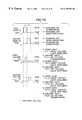
- FIG. 1is a cross sectional view showing an exposing device according to a first embodiment of the present invention
- FIG. 2is a cross sectional view taken along line A—A shown in FIG. 1;
- FIG. 3is a cross sectional view showing a state in which the exposing device shown in FIG. 1 is being operated;
- FIGS. 4 (A) and 4 (B)are diagrams for making a comparison between surface exposure using a related exposing device and digital multi-exposure using the exposing device shown in FIG. 1;
- FIG. 5is a plan view showing a light modulator unit according to the second embodiment of the present invention.
- FIG. 6is a cross sectional view taken along line A—A shown in FIG. 5;
- FIG. 7is a cross sectional view taken along line B—B shown in FIG. 5;
- FIG. 8is circuit diagram equivalent to the pixel portion shown in FIG. 5;
- FIG. 9is a cross sectional view showing a light modulator unit of an exposing device according to a third embodiment of the present invention.
- FIG. 10is a cross sectional view showing a state in which the exposing device shown in FIG. 9 is being operated.
- FIG. 11is a plan view showing a light modulator unit of an exposing device according to a fourth embodiment of the present invention.
- FIG. 12is a cross sectional view taken along line A—A shown in FIG. 11;
- FIG. 13is a cross sectional view taken along line B—B shown in FIG. 11;
- FIG. 14is a cross sectional view showing a state in which the exposing device shown in FIG. 11 is being operated;
- FIG. 15shows a spectral characteristic of a low-pressure mercury lamp for black light
- FIG. 16shows a spectral characteristic of transmittance of a light modulator incorporating the low-pressure mercury lamp shown in FIG. 15;
- FIG. 17shows a spectral characteristic of a backlight incorporating a low-pressure mercury lamp
- FIG. 18shows a spectral characteristic of transmittance of the light modulator incorporating the low-pressure mercury lamp shown in FIG. 17;
- FIG. 19is a perspective view showing a light modulator unit of an exposing device according to a fifth embodiment of the present invention.
- FIG. 20is a cross sectional view showing the light modulator unit shown in FIG. 19;
- FIG. 21is a cross sectional view showing a state in which the exposing device shown in FIG. 19 is being operated.
- FIG. 22is a cross sectional view showing an exposing device according to a sixth embodiment of the present invention.
- FIG. 23is a cross sectional view showing a first modification of the sixth embodiment
- FIG. 24is a cross sectional view showing a second modification of the sixth embodiment.
- FIG. 25is a cross sectional view showing a flat light source for use in an exposing device according to a seventh embodiment of the present invention.
- FIG. 26is a diagram showing light emitted from the flat light source shown in FIG. 25;
- FIG. 27is a cross sectional view showing a first modification of the seventh embodiment
- FIG. 28is a cross sectional view showing a second modification of the seventh embodiment
- FIG. 29is a cross sectional view showing an exposing device according to an eighth embodiment of the present invention.
- FIG. 30is a cross sectional view showing a flat display unit according to a ninth embodiment of the present invention.
- FIG. 31is a cross sectional view taken along line A—A shown in FIG. 31;
- FIG. 32is a cross sectional view showing a state in which the flat display unit shown in FIG. 31 is being operated;
- FIG. 33is a cross sectional view showing a filter section for use in a flat display unit according to a tenth embodiment of the present invention.
- FIG. 34is a cross sectional view showing a flat display unit according to an eleventh embodiment of the present invention.
- FIG. 35is a cross sectional view showing an array-type exposing device according to a twelfth embodiment of the present invention.
- FIG. 36is a cross sectional view showing a first modification of the twelfth embodiment
- FIG. 37is a cross sectional view showing a second modification of the twelfth embodiment
- FIG. 38is a cross sectional view showing an array-type exposing device according to a thirteenth embodiment of the present invention.
- FIG. 39is a cross sectional view showing a first modification of the thirteenth embodiment.
- FIG. 40is a perspective view showing an array-type exposing device according to a fourteenth embodiment of the present invention.
- FIG. 41is a cross sectional view showing the array-type exposing device shown in FIG. 40;
- FIGS. 42 (A) and 42 (B)are cross sectional views showing states in which the array-type exposing device shown in FIG. 40 is being operated;
- FIG. 43is a cross sectional view showing a first modification of the fourteenth embodiment
- FIG. 44is a cross sectional view taken along line A—A shown in FIG. 43;
- FIGS. 45 (A) and 45 (B)are plan views showing states in which the array-type exposing device shown in FIG. 43 is being operated;
- FIGS. 46 (A) and 46 (B)are cross sectional views of FIGS. 45 (A) and 45 (B) respectively;
- FIG. 47is a cross sectional view showing an array-type exposing device according to a fifteenth embodiment of the present invention.
- FIGS. 48 (A) and 48 (B)are plan views showing examples of a light shielding film of the array-type exposing device shown in FIG. 47;
- FIGS. 49 (A) and 49 (B)are cross sectional views showing states in which the array-type exposing device shown in FIG. 47 is being operated;
- FIG. 50is a cross sectional view showing an array-type exposing device according to a sixteenth embodiment of the present invention.
- FIGS. 51 (A) and 51 (B)are plan views showing examples of an opening of the array-type exposing device shown in FIG. 50;
- FIGS. 52 (A) and 52 (B)are cross sectional views showing states in which the array-type exposing device shown in FIG. 50 is being operated;
- FIG. 53is a cross sectional view showing a first modification of the sixteenth embodiment
- FIG. 54is a cross sectional view showing a second modification of the sixteenth embodiment
- FIG. 55is a cross sectional view showing a third modification of the sixteenth embodiment.
- FIG. 56is a cross sectional view showing an array-type exposing device according to a seventeenth embodiment of the present invention.
- FIG. 57is a cross sectional view showing a first modification of the seventeenth embodiment
- FIG. 58is a cross sectional view showing an array-type exposing device according to an eighteenth embodiment of the present invention.
- FIG. 59is a cross sectional view showing an array-type light modulator according to a nineteenth embodiment of the present invention.
- FIG. 60is a cross sectional view showing a state in which the array-type light modulator shown in FIG. 59 is being operated;
- FIG. 61is a plan view showing an array-type light modulator according to a twentieth embodiment of the present invention.
- FIG. 62is a hysteresis graph showing a relationship of light transmittance of a diaphragm incorporated in an array-type light modulator according to a twenty-first embodiment of the present invention and voltage applied thereto;
- FIG. 63is a plan view showing an array-type light modulator having light modulator units arranged in a matrix configuration
- FIG. 64is a table showing voltages between electrodes of the light modulator units derived from combinations of voltages of scan electrodes and voltages of signal electrodes;
- FIG. 65is a diagram showing a method of writing data by applying voltages having different waveforms to light modulator units arranged in the matrix configuration
- FIG. 66is a plan view showing a simple matrix according to a first modification of the twenty-first embodiment
- FIG. 67is a plan view showing an array-type light modulator according to a twenty-second embodiment of the present invention.
- FIG. 68is a table showing transmitted light intensity values derived from combinations of states of respective light modulator unit of the array-type light modulator shown in FIG. 67;
- FIG. 69is a diagram showing an equivalent circuit of a pixel portion of an array-type light modulator according to a twenty-third embodiment of the present invention.
- FIG. 70is a diagram showing an equivalent circuit of a pixel portion of an array-type light modulator according to a twenty-fourth embodiment of the present invention.
- FIG. 71is a diagram showing an equivalent circuit of a pixel portion of active matrix arrangement
- FIG. 72is a diagram showing a data writing method in which voltages having various waveforms are applied to respective light modulator units in matrix arrangement;
- FIG. 73is a diagram showing voltage applied to the respective light modulator units.
- FIG. 74is a diagram showing voltage applied to electrodes of the respective light modulator units.
- FIG. 1is a cross sectional view showing an exposing device according to a first embodiment of the present invention.
- FIG. 2is a cross sectional view taken along line A—A shown in FIG. 1 .
- a plurality of parallel and transparent electrodes (signal electrodes) 3 formed into elongated shapesare formed on a light guide plate 1 such that the signal electrodes 3 are positioned apart from one another.
- Supporters 5 for separating the adjacent signal electrodes 3are formed on the light guide plate 1 .
- the supporters 5can be formed by, for example, etching a material which is the same as that for forming the light guide plate 1 .
- a UV ray lamp (a low-pressure mercury lamp) 7 serving as a light sourceis disposed on the side of the light guide plate 1 . A light beam emitted from the UV ray lamp 7 is transmitted to the surface (the upper surface in FIG. 1) of the light guide plate 1 .
- a transparent flexible thin film 9is formed on the upper surface of the supporters 5 at a position apart from the signal electrodes 3 . Therefore, gaps 11 are formed between the signal electrodes 3 and the flexible thin film 9 .
- a plurality of other electrodes (scan electrodes) 13 formed into transparent and elongated shapesare formed on the upper surface of the flexible thin film 9 in a direction perpendicular to the signal electrodes 3 .
- the plural scan electrodes 13are formed in parallel with one another and apart from one another. That is, the signal electrodes 3 and the scan electrodes 13 are arranged in perpendicular directions so that a lattice configuration is formed, as shown in FIG. 2 .
- the light guide plate 1 , the signal electrodes 3 , the flexible thin film 9 and the scan electrodes 13constitute a light modulator unit 14 .
- a power source 15is connected to the signal electrodes 3 and the scan electrodes 13 .
- the power source 15is able to selectively apply a voltage to a predetermined electrode in accordance with image information.
- a transparent front plate 17is disposed above the light modulator unit 14 .
- An exposing device 19 structured as described aboveincorporates the light guide plate 1 which is constituted by a resin film made of polyethylene terephthalate or polycarbonate as well as transparent glass.
- the signal electrodes 3 and the scan electrodes 13are made of transparent and conductive materials.
- the transparent electrodesare made of materials which permit transmission of UV rays or the same have an optical characteristic which permits the transmission.
- the transparent electrodesare made of a metal material made to be transparent by a particulating process or a metal compound having conductivity.
- the metal materialmay be gold, silver, palladium, zinc or aluminum.
- the metal compoundmay be indium oxide, zinc oxide or aluminum-added zinc oxide (popularly called “AZO”).
- AZOaluminum-added zinc oxide
- a SnO 2 film (a Nesa film) or an ITO filmmay be employed.
- the signal electrodes 3 and the scan electrodes 13can be formed by laminating a thin film of the above-mentioned conductive material on the surface of the light guide plate 1 or the flexible thin film 9 by a sputtering method or a vacuum evaporation method. Then, the surface of the thin film is coated with resist, and then exposure and development are conducted. The exposure is performed such that a photomask is disposed on the photoresist Then, a UV ray is applied from a position above the photomask. The development is conducted by using development solution which is able to remove soluble portion of the photoresist.
- a power supply circuit which is connected to the signal electrodes 3 and the scan electrodes 13can be formed by using a pattern simultaneously with the process for forming the signal electrodes 3 and the scan electrodes 13 .
- FIG. 3is a cross sectional view showing a state in which the exposing device shown in FIG. 1 is being operated.
- the exposing device 19is able to perform digital multi-exposure, high-speed recording (typing or printing) can be performed when it is employed in an image recording apparatus (a printer, a duplicator or the like) which forms an image by exposing.
- an image recording apparatusa printer, a duplicator or the like
- a printer incorporating a related exposing devicehas a structure that a predetermined area is exposed to light in a predetermined time, as shown in FIG. 4 (A). Therefore, the relative movement between the exposing device and the image forming member is interrupted.
- a printer incorporating the exposing device 19has a structure that the flexible thin films 9 corresponding to each matrix electrode are selectively operated so that the digital multi-exposure is permitted. Therefore, line control is performed while the exposing device 19 and the image forming member are being relatively moved, as shown in FIG. 4 (B). Thus, high speed exposure can be performed, causing the recording speed to considerably be raised.
- the exposing device 19may be employed in DDCP (Digital Direct Color Proof) which is combination of an electrophotographic technique and an offset printing technique or CTP (Computer-To-Plate) for performing transference by directly forming an image on a plate.
- DDCPDigital Direct Color Proof
- CTPComputer-To-Plate
- the above-mentioned exposing device 19does not use a laser beam which raises the cost of the apparatus but uses a low cost UV ray lamp 7 .
- a high speed digital multi-exposurecan be performed.
- the light guide plate 1 , the signal electrodes 3 and the supporters 5can be formed into an array structure by etching. Thus, the manufacturing cost can be reduced.
- required operation voltagecan be lowered as compared with the exposure using a laser beam.
- the exposing device 19may be provided with color filters and interference filters for selecting wavelengths in anywhere of the optical paths.
- the light modulator unit 14 of the exposing device 19may be formed integrally such that the light guide plate 1 is used as the substrate or may be formed individually.
- the light modulator unit 14 of the exposing device 19may be structured such that the overall body is sealed by enclosing a rare gas after deaeration so as to prevent an influence of disturbance so that a stable structure is formed.
- FIG. 5is a plan view showing a light modulator unit according to the second embodiment.
- FIG. 6is a cross sectional view taken along line A—A shown in FIG. 5 .
- FIG. 7is a cross sectional view taken along line B—B shown in FIG. 5 .
- FIG. 8is a diagram showing an equivalent circuit of a pixel portion shown in FIG. 5 .
- An exposing deviceis able to perform the simple matrix operation.
- the exposing devicemay be performed by an active operation.
- the exposing device 21incorporates an active device (for example, TFT) 23 for each pixel.
- the TFT 23is composed of a gate electrode 25 , an insulating film 27 , an a-Si:H layer 29 , an electrode (a drain electrode) 31 and another electrode (a source electrode) 33 .
- the TFT 23is formed on a substrate 35 .
- a pixel electrode 37is connected to the source electrode 33 of the TFT 23 .
- An image signal line 39 for each columnis connected to the drain electrode 31 .
- a scan signal line 41 for each rowis connected to the gate electrode 25 .
- the pixel electrode 37is laminated on the flexible thin film 9 in the light modulator unit 43 .
- the flexible thin film 9is bridged between the supporters 5 .
- another electrode (a common electrode) 47which is applied with potential V com is provided for the substrate 35 to be opposite to the pixel electrode 37 .
- a voltage for electrically conducting the TFT 23is applied to the scan signal line 41 connected to the gate electrode 25 .
- a voltage for a required image signalis applied to an image signal line 39 connected to the drain electrode 31 , the drain electrode 31 and the source electrode 33 are conducted to each other. Therefore, the voltage of the image signal is applied to the pixel electrode 37 .
- the voltage of the potential V com of the common electrode 47 and the potential of the pixel electrode 37causes electrostatic stress to act. As a result, required modulation of light can be performed.
- FIG. 9is a cross sectional view showing a light modulator unit of the exposing device according to the third embodiment.
- FIG. 10is a cross sectional view showing a state in which the exposing device shown in FIG. 9 is being operated.
- the principle for modulating light by the electro-mechanical operation of the flexible thin filmmay use a light guide diffusion effect (hereinafter called “light guide diffusion”) by separating the flexible thin film and the transparent signal electrode from each other or bringing the same into contact with each other.
- the light guide diffusionuses the gap as a transmission resistance for light. When a gap is formed, light emitted from the signal electrode is intercepted or attenuated. Only when the flexible thin film is brought into contact with the signal electrode, light emitted from the signal electrode is transmitted (mode coupling) to the flexible thin film. The transmitted light beam is diffused by the flexible thin film so that the intensity of light emitted from the flexible thin film is controlled (light is modulated).
- an electrode 51 which is transparent with respect to a UV rayis formed on a light guide plate 1 .
- a metal oxidesuch as ITO, having a high electron density, a very thin metal film (made of aluminum), a thin film in which metal particles are dispersed in a transparent insulating member or a wide band gap semiconductor in which high concentration doping has been performed is employed.
- Insulating supporters 5are formed on the electrode 51 .
- the supporters 5may be made of, for example, a silicon oxide, a silicon nitride, ceramic or resin.
- a diaphragm 53is formed on the upper surface of the supporters 5 .
- Gaps (cavities) 11are formed between the electrode 51 and the diaphragm 53 .
- the diaphragm 53may be made of a semiconductor, such as polysilicon, an insulating silicon oxide, a silicon nitride, ceramic or resin. It is preferable that the refractive index of the diaphragm 53 is the same as that of the light guide plate 1 or superior to that of the light guide plate 1 .
- a light diffusion layer 55is formed on the diaphragm 53 , the light diffusion layer 55 being formed into a structure in which irregularities are formed on the surface of an inorganic or organic transparent material, a structure having a microprism or a microlens or a structure in which an inorganic or organic porous material or particles having different refractive indexes are dispersed in a transparent base.
- Another electrode 57 which is transparent with respect to a UV rayis formed on the light diffusion layer 55 .
- the material for making the electrode 51may be employed.
- the diaphragm 53 , the light diffusion layer 55 and the electrode 57constitute the flexible thin film.
- the gaps 11exist between the light guide plate 1 and the diaphragm 53 .
- the gaps 11is substantially determined by the height of the supporters 5 . It is preferable that the height of the gaps 11 is about 0.1 ⁇ m to about 10 ⁇ m.
- the gaps 11are usually formed by etching a sacrifice layer.
- the diaphragm 53 and the light diffusion layer 55are made of the same material.
- the diaphragm 53is constituted by a silicon nitride film and irregularities are formed on the upper surface. In this case, the diffusing function can be realized.
- a casewill be considered in which the voltage of the two electrodes 51 and 57 is zero and the gaps 11 (for example, air) exist between the diaphragm 53 and the light guide plate 1 when supply of the voltage is interrupted.
- the gaps 11for example, air
- the critical angle ⁇ c of the total reflectionis as follows:
- the UV raytravels forwards in the light guide plate 1 while the same is being totally reflected as shown in FIG. 9 when an incidence angle ⁇ c on the interface satisfies ⁇ > ⁇ C .
- the UV raytransmits to the diaphragm 53 , as shown in FIG. 10 . Then, the UV ray is diffused by the light diffusion layer 55 so as to be emitted over the surface.
- the exposing device 61is able to modulate light by controlling the position of the diaphragm 53 by applying voltage.
- the electrode 51which is transparent with respect to a UV ray is disposed between the light guide plate 1 and the diaphragm 53 , no problem for the operation arises if the electrode 51 has a thickness (2000 ⁇ ) of a usual thin film.
- the exposing device 61 according to this embodimentis able to change the distance between the diaphragm 53 and the light guide plate 1 and area of contact between the same by changing the voltage level. As a result, the amount of light transmission can be controlled. By using the above-mentioned effect, gradient control can be performed by changing the applied voltage.
- Fabry-Perot interferenceAs the basic principle for modulating light by causing the flexible thin film to perform the electro-mechanical operation, Fabry-Perot interference may be used. With the Fabry-Perot interference, an incident ray repeats reflection and transmission so that the ray is divided into a multiplicity of light beams in a state in which two flat surfaces oppose each other. Thus, the light beams are made to be parallel beams. Transmitted light beams superimpose and interfere with one another at infinity. Assuming that the perpendicular of the surface and an angle made by the incident light is i, the difference between optical paths for two adjacent light beams is given by
- the flexible thin filmis moved to make the difference x in the optical path so that light emitted from the signal electrode portion is modulated so as to be emitted from the flexible thin film.
- FIGS. 11 to 18A specific example of an exposing device using the Fabry-Perot interference will now be described with reference to FIGS. 11 to 18 .
- FIG. 11is a plan view showing a light modulator unit of the exposing device according to the fourth embodiment.
- FIG. 12is a cross sectional view taken along line A-A shown in FIG. 11 .
- FIG. 13is a cross sectional view taken along line B-B shown in FIG. 11 .
- FIG. 14is a cross sectional view showing a state in which the exposing device shown in FIG. 11 is being operated.
- FIG. 15is shows the spectral characteristic of a low-pressure mercury lamp for black light.
- FIG. 16shows a spectral characteristic of transmittance of a light modulator incorporating the low-pressure mercury lamp shown in FIG. 15 .
- FIG. 17shows is a spectral characteristic of a backlight incorporating a low-pressure mercury lamp.
- FIG. 18shows a spectral characteristic of transmittance of a light modulator incorporating the low-pressure mercury lamp shown in FIG. 17 .
- a dielectric multilayer-film mirror 73is disposed on a substrate 71 which is transparent with respect to a UV ray.
- a pair of electrodes 75are formed on the two sides of the substrate 71 such that the dielectric multilayer-film mirror 73 is interposed.
- Supporters 5are disposed at the right and left (right and left portions in FIG. 11) portions of the electrodes 75 .
- a diaphragm 53is disposed on the upper surfaces of the supporters 5 .
- a dielectric multilayer-film mirror 77is formed on the lower surface of the diaphragm 53 opposing the dielectric multilayer-film mirror 73 .
- Gaps 11are formed between the dielectric multilayer-film mirror 73 and the dielectric multilayer-film mirror 77 .
- Another pair of electrodes 79are formed on the diaphragm 53 to oppose the electrodes 75 .
- reference numeral 80denotes a spacer.
- a UV ray lamp (a low-pressure mercury lamp) 83 for black lightis disposed on the side of the plate-like flat light source 81 .
- a flat light source unit 81receives the UV ray emitted from the low-pressure mercury lamp 83 for black light through the side surface thereof to emit the same to the surface thereof.
- the spectral characteristic of the emitted UV rayis as shoen in FIG. 15 . That is, central wavelength ⁇ 0 exists in the vicinity of 360 nm.
- the foregoing UV rayis used as a backlight beam.
- the height of the gaps 11 when no voltage is suppliedis t off (in the left-hand state shown in FIG. 14 ).
- the heightcan be controlled when the device is manufactured.
- the height of the gaps 11is shortened by dint of the electrostatic force when voltage has been applied.
- the short heightis made to be t on (in the right-hand state shown in FIG. 14 ).
- Control of t oncan be performed by adjusting the balance between the applied electrostatic stress and the restoring force which is generated when the diaphragm 53 has been deformed.
- the spacer 80may be formed on the electrode to make constant the displacement.
- the spaceris made of an insulating material, the dielectric constant (1 or greater) of the insulating material attains an effect of lowering the applied voltage. If the spacer is made of a conductive material, the foregoing effect can furthermore be enhanced.
- the electrodes and the spacermay be made of the same material.
- the light intensity reflectance R of each of the dielectric multilayerfilm mirrors 73 and 77are 0.85.
- the exposing device 91 having the light modulator unit 85is able to deflect the diaphragm 53 to obtain a multilayer film interference effect.
- the UV raycan be modulated.
- an arbitrary combinationmay be employed among the height t and refractive index n of the gaps 11 and light intensity reflectance R of the dielectric multilayer-film mirrors 73 and 77 .
- the central wavelength of the transmissive spectrumcan arbitrarily be changed.
- the amount of light transmittancecan continuously be controlled. That is, gradient control by changing the applied voltage can be performed.
- a backlightcomprising a low-pressure mercury lamp may be employed in place of the above-mentioned low-pressure mercury lamp 83 for black light.
- a main component of the spectral characteristic of direct light of the low-pressure mercury lampis a line spectrum of 254 nm.
- a backlight unitis constituted.
- the other wavelengthsare cut by a filter or the like.
- the spectral characteristic of the UV ray backlightis as shown in FIG. 17 .
- the light modulator unithas an effective pixel area which is made of materials (the diaphragm, the dielectric multilayer film mirror and the substrate) which permit transmission of UV ray having a wavelength of 254 nm.
- an arbitrary combinationmay be employed among the height t and refractive index n of the gaps 11 and light intensity reflectance R of the dielectric multilayer-film mirrors 73 and 77 .
- this modificationis able to arbitrarily change the central wavelength of the transmissive spectrum when the height t is continuously changed by changing the voltage.
- the amount of light transmittancecan continuously be controlled. That is, gradient control can be performed by changing the applied voltage.
- FIG. 19is a perspective view showing a light modulator unit of the exposing device according to the fifth embodiment.
- FIG. 20is a cross sectional view showing the light modulator unit shown in FIG. 19 .
- FIG. 21is a cross sectional view showing a state in which the exposing device shown in FIG. 19 is being operated.
- a transparent electrode 103 which is transparent with respect to a UV rayis formed on a substrate 101 which is transparent with respect to the UV ray.
- the substrate 101is covered with an insulating light shielding film 105 except for an opening through which light is allowed to pass so that light is shielded.
- An insulating film 107is formed on the surfaces of the transparent electrode 103 and the light shielding film 105 .
- Insulating supporters 109are disposed on the two sides of an opening formed in the substrate 101 .
- a light shielding plate 111which is a flexible thin film is disposed at the top ends of the supporters 109 .
- the light shielding plate 111is formed into a cantilever structure and made of a conductive material which absorbs or reflects UV rays.
- the cantilever and conductive light shielding plate 111may be formed by a single thin film or a plurality of thin films.
- the shape of the light shielding plate 111corresponds to the shape of the opening.
- the light shielding plate 111is somewhat larger than the opening.
- the exposing device 115 having a light modulator unit 113 structured as described aboveis disposed on the flat light source unit 81 .
- the light shielding plate 111opposes the opening.
- a UV ray allowed to pass through the openingis absorbed or reflected by the light shielding plate 111 (in a left-hand state in FIG. 21 ).
- the degree of inclination of the light shielding plate 111that is, the amount of light transmission can continuously be changed.
- the gradientcan be controlled by changing the applied voltage.
- the above-mentioned exposing device 115has the structure that the light shielding plate 111 can be deflected to change the path for UV rays. As a result, UV rays can be modulated.
- FIG. 22is a cross sectional view showing an exposing device according to the sixth embodiment.
- FIG. 23is a cross sectional view showing a first modification of the sixth embodiment.
- FIG. 24is a cross sectional view showing a second modification of the sixth embodiment.
- the exposing device 121is, as shown in FIG. 22, provided with a plurality of signal electrodes 3 disposed on the surface of a transparent substrate 122 adjacent to the UV source. Supporters 5 are disposed between adjacent signal electrodes 3 . A flexible thin film 9 is bridged between upper surfaces of the supporters 5 . Gaps 11 are formed between the signal electrodes 3 and the flexible thin film 9 . Scan electrodes 13 are formed on the surface of the flexible thin film 9 . A front transparent substrate 123 is formed on the front surface of the emission side of each of the scan electrodes 13 .
- a black mask 127is formed in a boundary between adjacent pixels 125 on a surface of the filter 123 opposing the scan electrodes 13 .
- the black mask 127shields light leakage from the boundary of the pixels to raise the contrast effect.
- the exposing device 121has a light modulator unit 128 composed of the signal electrodes 3 , the gaps 11 , the flexible thin film 9 , the scan electrodes 13 and the black mask 127 .
- the exposing device 121incorporates the transparent substrate 123 on the front surface thereof, an UV ray image obtained by the light modulator unit 128 of the exposing device 121 can be projected and exposed to a sensitive material by a projecting lens.
- the exposing devicemay be provided with a fiber face plate 129 as shown in FIG. 23 in place of the front transparent substrate 123 .
- An exposing device 121 a having the above-mentioned structureis able to perform contact exposure with a sensitive material in addition to the above-mentioned exposure.
- the exposing devicemay be provided with a distributed refractive index lens (for example, “SELFOC lens” which is trade name).
- SELFOC lenswhich is trade name.
- the SELFOC lens 131serves as a lens because its refractive index is continuously changed.
- An exposing device 121 b of the foregoing typeis able to perform exposure such that the distance from the sensitive material is sufficiently shortened in addition to the above-mentioned exposure.
- FIG. 25is a cross sectional view showing a flat light source for use in the exposing device according to the seventh embodiment.
- FIG. 26is a diagram showing light emitted from the flat light source shown in FIG. 25 .
- FIG. 27is a cross sectional view showing a first modification of the seventh embodiment.
- FIG. 28is a cross sectional view showing a second modification of the seventh embodiment.
- a flat light source unit for the exposing devicemay be formed into any one of a variety of structures.
- a flat light source unit 141may be composed of a UV ray lamp (a low-pressure mercury lamp) 143 , a UV ray reflecting plate 145 , a light conducting plate 147 , a diffusing plate 149 and a light collecting plate 151 .
- a UV ray lampa low-pressure mercury lamp
- the low-pressure mercury lamp 143is disposed adjacent to an end of the light conducting plate 147 .
- a UV ray emitted from the low-pressure mercury lamp 143is made incident on the end of the light conducting plate 147 by the UV-ray reflecting plate 145 .
- the diffusing plate 149is disposed on the surface of the light conducting plate 147 .
- the light collecting plate 151is disposed on the surface of the diffusing plate 149 .
- a UV ray made incident on the end of the light conducting plate 147is allowed to pass through the diffusing plate 149 and the light collecting plate 151 , and then emitted.
- the above-mentioned flat light source unit 141is able to emit diffused light having directivity in a direction of a normal line of the plane, as shown in FIG. 26 .
- the flat light source unit 141may be suitably employed in the exposing devices 91 and 115 according to the fourth embodiment and the fifth embodiment, respectively.
- the flat light source unitmay be a collimated light source which emits to light in a direction substantially perpendicular to the light emitting surface, as shown in FIG. 27 .
- Collimated lightcan be emitted by a well-known technique.
- collimated lightcan be emitted.
- a flat light source unit 141 a for emitting collimated lightis able to convert light emitted from the light conducting plate 147 into parallel beams to give directivity.
- the flat light source unit 141 amay be suitably employed in the exposing devices 91 and 115 according to the fourth embodiment and the fifth embodiment, respectively.
- the flat light source unitmay be structured such that the UV-ray reflecting plate 145 around the lamp is inclined in order to make the optical path in the light conducting plate 147 to be higher than the critical angle for the total reflection so as to make incident a UV ray on the inside portion of the light conducting plate 147 .
- incident UV raystravel to an end while the UV rays are totally reflected by the light conducting plate 147 . Then, UV rays are reflected by a reflecting plate 153 . Then, UV rays are returned to the low-pressure mercury lamp 143 while UV rays are being totally reflected.
- the flat light source unit 141 benables a flat light source having no directivity to be obtained.
- the flat light source unit 141 bmay be employed in the exposing device 61 according to the third embodiment.
- the flat light source unitmay incorporate a light emitting device for emitting UV rays, for example, a dispersion-type inorganic EL (Electroluminescence), a thin film type inorganic EL, a low-molecule type organic EL, a high-molecule type organic EL, an inorganic semiconductor LED (Light Emitting Diode) or a FED (which causes a fluorescent member for emitting UV rays to emit light by discharged electrons).
- a light emitting device for emitting UV raysfor example, a dispersion-type inorganic EL (Electroluminescence), a thin film type inorganic EL, a low-molecule type organic EL, a high-molecule type organic EL, an inorganic semiconductor LED (Light Emitting Diode) or a FED (which causes a fluorescent member for emitting UV rays to emit light by discharged electrons).
- the light modulator unitWhen the light modulator unit are provided for the light emitting surfaces of the light emitting devices, light emitted from the light emitting device can directly be introduced into the light modulator unit.
- the flat light source unit incorporating the light emitting devicesenables uniform light emitting intensity to be realized with a compact structure.
- the required voltagecan be lowered in a case of the organic EL and the inorganic LED.
- the lifetime of the light source incorporating the inorganic LEDcan significantly be elongated.
- the lifetime of each the thin film inorganic EL, the organic EL and the FEDcan be elongated.
- FIG. 29is a cross sectional view showing the exposing device according to the eighth embodiment.
- the exposing device according to this embodimenthas a structure which is substantially similar to the exposing device 121 according to the sixth embodiment shown in FIG. 22 . Therefore, the same elements are given the same reference numerals and the same elements are omitted from description. As shown in FIG. 29, the exposing device 121 has a gap 163 from a black light unit 161 so that the exposing device 121 is separated from the black light unit 161 .
- Transparent substrates 122 and 123are substrates which permit transmission of at least UV rays. If the wavelength of the UV ray is 365 nm, it is preferable that the transparent substrate 122 and 123 are made of glass, acrylic resin or the like. When the wavelength of the UV ray is 245 nm, it is preferable that the transparent substrates 122 and 123 are made of molten quartz.
- the exposing device 121has the structure that the gap 163 is formed between the transparent substrate 122 and the backlight unit 161 so that the light modulator unit and the light emitting portion are separated from each other. Therefore, the transparent substrate 122 and the backlight unit 161 can individually be manufactured. As compared with the exposing device 19 according to the first embodiment and having a structure that the signal electrodes 3 are directly provided for the light guide plate 1 , appropriate materials can be employed to manufacture the transparent substrate 122 and the light guide plate for the backlight unit, respectively. As a result, freedom to select materials can be improved.
- FIG. 30is a cross sectional view showing the flat display unit according to the ninth embodiment of the present invention.
- FIG. 31is a cross sectional view taken along line A—A shown in FIG. 30 .
- a plurality of parallel and transparent electrodes (signal electrodes) 1003 formed into elongated shapesare formed on a light guide plate 1001 such that the signal electrodes 1003 are positioned apart from one another.
- Supporters 1005 for separating the adjacent signal electrodes 1003are formed on the light guide plate 1001 .
- the supporters 1005can be formed by, for example, etching a material which is the same as that for forming the light guide plate 1001 .
- An ultraviolet-ray lamp (a low-pressure mercury lamp) 1007 serving as a light sourceis disposed on the side of the light guide plate 1001 . A light beam emitted from the UV ray lamp 1 is transmitted to the surface (the upper surface in FIG. 30) of the light guide plate 1001 .
- a transparent flexible thin film 1009is formed on the upper surface of the supporters 1005 at a position apart from the signal electrodes 1003 . Therefore, gaps 11 are formed between the signal electrodes 1003 and the flexible thin film 1009 .
- a plurality of other electrodes (scan electrodes) 1013 formed into transparent and elongated shapesare formed on the upper surface of the flexible thin film 1009 in a direction perpendicular to the signal electrodes 1003 .
- the plural scan electrodes 1013are formed in parallel with one another and apart from one another. That is, the signal electrodes 1003 and the scan electrodes 1013 are arranged in perpendicular directions so that a lattice configuration is formed, as shown in FIG. 31 .
- the light guide plate 1001 the signal electrodes 1003 , the flexible thin film 1009 and the scan electrodes 1013constitute a light modulator unit 1014 .
- a power source 1015is connected to the signal electrodes 1003 and the scan electrodes 1013 .
- the power source 1015is able to selectively apply a voltage to a predetermined electrode in accordance with image information.
- Elongated fluorescent members 1016 a , 1016 b and 1016 c in three primary colors (R, G, B)are disposed above the scan electrodes 1013 to be opposite to the signal electrodes 1003 .
- a black matrix (not shown) for raising the contrast ratio of the fluorescent membersmay be disposed among the fluorescent members 1016 a , 1016 b and 1016 c.
- a transparent front plate 1017is disposed above the fluorescent members 1016 a , 1016 b and 1016 c .
- the front plate 1017may be a color filter in a color which is the same as the color of the emitted fluorescence.
- a flat display unit 1019 structured as described aboveincorporates the light guide plate 1001 which is constituted by a resin film made of polyethylene terephthalate or polycarbonate as well as transparent glass.
- the signal electrodes 1003 and the scan electrodes 1013are made of transparent and conductive materials. It is preferable that the signal electrodes 1003 adjacent to the light guide plate 1001 are made of a material which permits transmission of an exciting UV ray or which has such an optical characteristic. It is preferable that the scan electrodes 1013 adjacent to the fluorescent members 1016 a , 1016 b and 1016 c is made of a material which permits transmission of the exciting UV ray. More effectively, the scan electrodes 1013 are made of a material which reflects the wavelength of the emitted fluorescence or which has such an optical characteristic.
- the transparent electrodesare made of a metal material made to be transparent by a particulating process or a metal compound having conductivity.
- the metal materialmay be gold, silver, palladium, zinc or aluminum.
- the metal compoundmay be indium oxide, zinc oxide or aluminum-added zinc oxide (popularly called “AZO”).
- AZOaluminum-added zinc oxide
- a SnO 2 film (a Nesa film) or an ITO filmmay be employed.
- the signal electrodes 1003 and the scan electrodes 1013can be formed by laminating a thin film of the above-mentioned conductive material on the surface of the light guide plate 1001 or the flexible thin film 1009 by a sputtering method or a vacuum evaporation method. Then, the surface of the thin film is coated with resist, and then exposure and development are conducted. The exposure is performed such that a photomask is disposed on the photoresist. Then, a UV ray is applied from a position above the photomask. The development is conducted by using development solution which is able to remove a soluble portion of the photoresist.
- FIG. 32is a cross sectional view showing a state in which the flat display unit according to the present invention is being operated.
- the flat display unit 1019has the structure that a light beam transmitted from the light guide plate 1001 is allowed to pass through only the pair of the transparent electrodes interposing the gaps 1011 .
- the fluorescent members 1016 a , 1016 b and 1016 care excited.
- the efficiency of using lightcan be improved.
- the angle of the field of viewcan be enlarged as compared with a liquid crystal display unit which permits transmission of light by dint of excitation of liquid crystal molecules.
- the quality of an imagedoes not depend on the regular arrangement of the multiple electrodes.
- an image having a high qualitycan easily be obtained.
- the necessity of forming insulation wall for the plasma display unit for the purpose of generating plasma for each pixel and realizing high vacuumcan be eliminated. Therefore, weight reduction and enlargement of the area can easily be performed. Thus, the manufacturing cost can be reduced.
- the light guide plate 1001 , the signal electrodes 1003 and the supporters 1005can be formed into an array structure by etching. Thus, the manufacturing cost can be reduced.
- the flexible thin film 1009can preform electro-mechanical operation using the Coulomb force, the voltage required to operate the unit can be lowered as compared with the plasma display unit which generates plasma and the FED which accelerates emitted electrons and applies the same to the fluorescent members.
- the light modulator unit 1014 of the flat display unit 1019may be formed integrally such that the light guide plate 1001 is used as a substrate or the same may be formed individually.
- the light modulator unit 1014 of the flat display unit 1019may be structured such that the overall body is sealed by enclosing a rare gas after a deaeration operation so as to prevent an influence of disturbance so that a stable structure is formed.
- FIG. 33is a cross sectional view showing a filter portion for use in the flat display unit according to the tenth embodiment.
- the flat display unitmay be provided with a variety of filters.
- a film (a filter) 1121is provided between the light modulator unit and fluorescent members 1016 a , 1016 b and 1016 c .
- the filter 1121is in the form of a film which permits transmission of UV rays and reflects visible rays.
- the filmmay be an interference film (a dielectric multilayer film or a metal dielectric multilayer film) which reflects UV rays, a film made of a single material ( ⁇ -alumina or ⁇ -alumina) or a composite film of the foregoing materials.
- Reference numeral 1127 in the drawingrepresents a black matrix formed in the boundaries among the adjacent fluorescent members 1016 a , 1016 b and 1016 c.
- the fluorescent members 1016 a , 1016 b and 1016 care irradiated with UV rays.
- visible raysare scattered and caused to emit light. Light rays of the visible rays scattered toward the light modulator unit is reflected by the filter 1121 toward the surface so that a high displaying efficiency is realized.
- a film (a filter) 1123is formed on the surfaces of the fluorescent members 1016 a , 1016 b and 1016 c .
- the filter 1123is in the form of a film which reflects or absorbs UV rays and permits transmission of visible rays.
- the filtermay be a sharp cut filter which absorbs UV rays or an interference film (a dielectric multilayer film or a metal dielectric multilayer film) which reflects UV rays.
- the flat display unit incorporating the filter 1123is able to prevent emission of harmful UV rays over the display surface.
- the UV rays reflected by the filter 1121can be reflected again and thereby the UV rays are reused for the excitation of the fluorescent members so that a high displaying efficiency is realized.
- the positions of the filters 1121 and 1123are not limited to the above-mentioned positions.
- the filter 1121may be disposed in the light modulator unit.
- the filter 1123may be disposed adjacent to the surface of the front transparent substrate 1125 which is transparent with respect to visible rays.
- a flat display unit according to an eleventh embodiment of the present inventionwill now be described.
- FIG. 34is a cross sectional view showing the flat display unit according to the eleventh embodiment.
- the flat display unit according to this embodimenthas a structure which is substantially similar to the flat display unit 1019 according to the ninth embodiment shown in FIG. 30 . Therefore, the same elements are given the same reference numerals and the same elements are omitted from description.
- reference numeral 1127represents a black matrix formed in the boundaries among adjacent fluorescent members 1016 a , 1016 b and 1016 c .
- the flat display unit 1161has a gap 1165 from the backlight unit 1163 so that the separate configuration is employed.
- a substrate 1167 in the light modulator unitmust be a substrate which permits transmission of at least UV rays. If the wavelength of the UV ray is 365 nm, it is preferable that the substrate 1167 is made of glass, acrylic resin or the like. When the wavelength of the UV ray is 245 nm, it is preferable that the substrate 1167 is made of molten quartz. It is preferable that a substrate 1169 adjacent to the front fluorescent member is a substrate (made of usual glass) which permits transmission of visible rays.
- the flat display unit 1161has the structure that the gap 1165 is formed between the substrate 1167 and the backlight unit 1163 so that the light modulator unit and the light emitting portion are separated from each other. Therefore, the substrate 1167 and the backlight unit 1163 can individually be manufactured. As compared with the flat display unit 1019 according to the ninth embodiment and having a structure that the signal electrodes 1003 are directly provided for the light guide plate 1001 , appropriate materials can be employed to manufacture the substrate 1167 and the light conducting plate for the backlight unit, respectively. As a result, freedom to select materials can be improved.
- FIG. 35is a cross sectional view showing the array-type exposing device according to the twelfth embodiment.
- a transparent substrate 2003 which is transparent with respect to a UV rayis disposed adjacent to the emission side of a flat light source 2001 which emits UV rays, the transparent substrate 2003 being distant from the flat light source 2001 for a predetermined distance and in parallel with the flat light source 2001 .
- the flat light source 2001comprises a UV ray lamp (not shown) disposed on the side surface of a light guide plate (not shown). In the flat light source 2001 , light emitted from the ultraviolet-ray lamp is guided upwards in FIG. 35 and emitted.
- a light modulator unit 2005is formed on the surface of the transparent substrate 2003 opposite to the flat light source 2001 .
- the light modulator unit 2005is disposed one-dimensionally or two-dimensionally.
- the light modulator unit 2005has a non-opened portion 2007 .
- the nonopened portion 2007is divided into regions S each having an area corresponding to one pixel.
- Each non-opened portion 2007has an opening 2009 having an area which is smaller than that of one pixel.
- the openings 2009are formed in the central portion of the each non-opened portion 2007 .
- the non-opened portion 2007shields light allowed to pass through the transparent substrate 2003 . Therefore, light emitted from the flat light source 2001 is allowed to pass through only the openings 2009 , and then emitted from the light modulator unit 2005 .
- Microlenses 2011 as a light converging memberare so formed on the surface of the transparent substrate 2003 adjacent to the flat light source 2001 as to correspond to the non-opened portions 2007 , that is, to pixels.
- the microlenses 2011 according to this embodimentare formed into convex shapes facing the flat light source 2001 .
- the microlenses 2011converge light made incident from the flat light source 2001 to the openings 2009 of the light modulator unit 2005 .
- the microlenses 2011may be lenses which use refraction of a transparent member at an end surface of refraction, lenses which use refraction of continuously distributed refractive indexes on the inside (distributed refractive index lenses) or lenses (grating lenses) which uses diffraction of light occurring by dint of a periodical structure.
- the microlenses 2011may be a one-dimensional lens array constituted by one-dimensionally arranging a plurality of distributed refractive index lenses in the form of semi-spheres at the same intervals or a flat micro-lenses constituted by arranging the same two-dimensionally at the same intervals.
- the flat micro-lensis a device from which a function as a lens can be obtained by realizing distribution of refractive indexes in the vicinity of the surface of a glass plate.
- a film made of a metal material or the likeis deposited on the surface of a multi-component glass.
- circular openingsare formed by lithography so that a mask is obtained.
- ion exchangeis performed to raise the refractive indexes of semi-spherical regions below the circular openings.
- an action of the lenscan be realized for light perpendicularly made incident on the substrate.
- the foregoing lenshas an advantage in that a one-dimensional or two-dimensional lens array can easily be mass-produced.
- the array-type exposing device 2013has the structure that the non-opened portion 2007 corresponding to one pixel has the openings 2009 each having an area smaller than that of the nor-opened portion 2007 , the numeric aperture can be reduced.
- the light modulating mechanism of the light modulator unit 2005 for modulating light by a deflecting operation (an electro-mechanical operation) of the flexible thin film by dint of the electrostatic stresscan be reduced.
- the mass of a movable member (the flexible thin film)can be reduced.
- the operation speedcan be raised.
- the array-type exposing devicemay have a structure that the microlenses 2011 are disposed individually from the light modulator unit 2005 .
- the microlenses 2011may be provided for a position adjacent to the flat light source 2001 .
- the light beammay be diffused light having directivity in a direction of a normal line of the surface.
- the front surface of the light modulator unit 2005may be provided with an image forming lens or a distributed refractive index lens (for example, the SELFOC lens).
- FIG. 36is a cross sectional view showing a first modification of the twelfth embodiment.
- An array-type exposing device 2015 according to the first modificationhas a structure that region S having an area corresponding to one pixel is divided into a plurality of regions m. Therefore, non-opened portions 2017 and microlenses 2019 are formed to correspond to the regions m.
- the non-opened portions 2017incorporate openings 2021 having areas smaller than those of the non-opened portions 2017 .
- the other structuresare the same as those of the array-type exposing device 2013 according to the twelfth embodiment.
- the size of the light modulator unit 2023 of the array-type exposing device 2015can furthermore be reduced, the operation speed can be raised. Since the size of the mechanism can be reduced, the design freedom of the light modulator unit 2023 can be enhanced. Since the microlenses 2019 converge light, efficient and bright exposure can be performed even if the area of the opening is very small.
- the first modificationhas the structure that the region S having the area corresponding to one pixel is furthermore divided into the plural regions m. Therefore, area gradient exposure can be performed with a small area obtained by dividing one pixel.
- FIG. 37is a cross sectional view showing a second modification of the twelfth embodiment.
- An array-type exposing device 2025 according to the second modificationhas a structure that the microlenses 2011 are disposed individually from the light modulator unit 2005 .
- the microlenses 2011 disposed individuallymay be disposed on the emission surface of the flat light source.
- Each of the microlenses 2011is disposed such that the optical axis coincides with the center of each of the openings 2009 , similarly to the array-type exposing device 2013 .
- the array-type exposing device 25has the structure that the light modulator unit 2005 and the microlenses 2011 are separated from each other, the transparent substrate 2003 and the microlenses 2011 can individually be manufactured. Therefore, freedom to select materials of the transparent substrate 2003 and the microlenses 2011 can be enhanced. That is, optimum materials can be selected to manufacture the transparent substrate 2003 and the microlenses 2011 .
- FIG. 38is a cross sectional view showing an array-type exposing device according to a thirteenth embodiment of the present invention.
- An array-type exposing device 2027 according to the thirteenth embodimenthas a structure that a transparent substrate 2031 having a fluorescent member 2029 is disposed opposite to the emission side of the light modulator unit 2005 of the array-type exposing device 2013 shown in FIG. 35 .
- the fluorescent member 2029has three primary color (R, G and B) portions 2029 a , 2029 b and 2029 c which correspond to the light modulator units 2005 .
- the transparent substrate 2031is made of a material which is transparent with respect to the wavelength of a fluorescence emitted from the fluorescent member 2029 .
- itcan be constituted by a resin film made of polyethylene terephthalate or polycarbonate, as well as a transparent glass plate.
- the array-type exposing device 2027 constituted as described abovehas the structure that light converged by the microlenses 2011 is introduced into the openings 2009 of the light modulator unit 2005 . Light introduced into the openings 2009 is exposed and controlled by the light modulator unit 2005 , and then allowed to collide with the fluorescent member 2029 . As a result, the array-type exposing device 2027 exposes a visible ray or an infrared ray one-dimensionally or two-dimensionally.
- the array-type exposing device 2027is able to constitute a flat display unit which incorporates the light modulator unit 2005 which modulates light emitted from the flat light source 2001 . Then, modulated light is used to cause the fluorescent member 2029 to perform a display with light.
- the flat display unit incorporating the array-type exposing device 2027has the structure that the fluorescent member 2029 is caused to emit light from the surface thereof. Therefore, the angle of the field of view can be enlarged as compared with a structure that light is allowed to pass through oriented liquid crystal molecules. Moreover, the necessity for the plasma display unit that an insulation wall is formed and a high vacuum is realized for the purpose of generating plasma can be eliminated. Therefore, weight reduction and enlargement of a displaying area can easily be performed.
- FIG. 39is a cross sectional view showing a first modification of the thirteenth embodiment.
- An array-type exposing device 2033 according to the first modificationhas a structure that a transparent substrate 2031 having a fluorescent member 2029 is added to the array-type exposing device 2015 according to the first modification of the twelfth embodiment shown in FIG. 36 .
- the array-type exposing device 2033has the structure that the region S having an area corresponding to one pixel is furthermore divided into a plurality of regions m.
- Each of fluorescent members 2029 a , 2029 b and 2029 c provided for the transparent substrate 2031has an area corresponding to one pixel. Therefore, the fluorescent members 2029 a , 2029 b and 2029 c in R, G and B correspond to one pixel composed of the plural regions m.
- the array-type exposing device 2033has the structure that the light modulator units 2023 corresponding to the regions m are controlled to set the brightness of each of the fluorescent members 2029 a , 2029 b and 2029 c corresponding to one pixel. Thus, gradient control can be performed.
- FIG. 40is a perspective view showing an array-type exposing device according to a fourteenth embodiment of the present invention.
- FIG. 41is a cross sectional view showing the array-type exposing device 2027 shown in FIG. 40 .
- FIGS. 42 (A) and (B)are cross sectional views showing states in which the array-type exposing device shown in FIG. 40 is being operated.
- a light modulator unit 2034 of an array-type exposing device 2035may be employed as the light modulator unit 2005 or 2023 of the array-type exposing devices 2013 , 2015 , 2025 , 2027 or 2033 according to the twelfth and thirteenth embodiments.
- a transparent electrode 2039 which is transparent with respect to a UV rayis disposed on a transparent substrate 2037 which is transparent with respect to a UV ray.
- the transparent electrode 2039is shielded by an insulating light shielding film 2043 except for an opening 2041 through which light is allowed to pass through. Therefore, the surface of the light shielding film 2043 except for the opening 2041 is made to be a non-opened portion 2045 .
- An insulating film 2047is formed on the surfaces of the transparent electrode 2039 and the opening 2041 .
- a pair of insulating supporters 2049are disposed on the two sides of the opening 2041 .
- a light shielding portion (a light shielding plate) 2051which is a flexible thin film is bridged between the two top ends of the supporters 2049 .
- the two ends of a beam 2051 a of the light shielding portion 2051are secured to the supporters 2049 .
- the light shielding portion 2051projects over the side end of the beam 51 a to cover the opening 2041 . That is, the light shielding portion 2051 is formed into a cantilever structure.
- the shape of the light shielding portion 2051is similar to the shape of the opening 2041 .
- the light shielding portion 2051is somewhat larger than the opening 2041 .
- the light shielding portion 2051is made of a conductive material which absorbs or reflects a UV ray.
- the light shielding portion 2051may be constituted by a single thin film or a plurality of thin films.
- any one of the following structuresmay be employed: a single structure composed of a thin metal film made of aluminum or chrome which reflects UV rays or a semiconductor, such as polysilicon which absorbs UV rays; a structure constituted by evaporating a material to an insulating film made of a silicon oxide or a silicon nitride or a thin semiconductor film made of polysilicon; or a composite structure constituted by evaporating a filter in the form of, for example, a dielectric multi-layer film.
- a microlens 2011 corresponding to the opening 2041is formed on the transparent substrate 2037 facing a flat light source (not shown).
- the array-type exposing device 2035 having the light modulator unit 2034 structured as described aboveis disposed on a flat light source (not shown).
- a flat light sourcenot shown.
- the light shielding portion 2051is opposite to the opening 2041 . Therefore, a UV ray allowed to pass through the opening 2041 is absorbed or reflected by the light shielding portion 2051 , as shown in FIG. 42 (A).
- the electrostatic stress acting between the two elementscauses the light shielding portion 2051 to be moved substantially perpendicularly with respect to the transparent substrate 2037 , as shown in FIG. 42 (B).
- the light shielding portion 2051is inclined toward the transparent electrode 2039 while it is being twisted. That is, the light shielding portion 2051 does not shield light.
- the UV ray allowed to pass through the opening 2041is able to further forward travel.
- the voltageis again made to be zero, the elasticity of the cantilever restores the light shielding portion 2051 to the original position.
- the light shielding portion 2051is deflected to change the path for the UV ray.
- UV rayscan be modulated.
- the degree of inclination of the light shielding portion 2051that is, the amount of light transmission can continuously be changed.
- the array-type exposing device 2035 incorporating the microlens 2011is able to converge light emitted from the flat light source. Therefore, also the light modulator unit 2034 having the non-opened portion 2045 is able to improve the efficiency of using light.
- the size of the opening 2041can be reduced because the microlens 2011 converges light, the size of the light shielding portion 2051 can be reduced. Therefore, a light modulator unit requiring low voltage and exhibiting a high speed response can be obtained. Since the size of the light shielding portion 2051 can be reduced, the amount of displacement occurring when the operation is performed can be reduced. As a result, fatigue of the material of the light shielding portion 2051 can be prevented. Thus, the durability and reliability of the light modulator unit can be improved.
- FIG. 43is a cross sectional view showing a first modification of the fourteenth embodiment.
- FIG. 44is a cross sectional view taken along line A—A shown in FIG. 43 .
- FIGS. 45 (A) and (B)are plan views showing states of the operation of the array-type exposing device shown in FIG. 43 .
- FIGS. 46 (A) and (B)are cross sectional views of FIGS. 45 (A) and (B), respectively.
- a light modulator unit 2057 of an array-type exposing device 2055 according to this modificationmay be employed as the light modulator unit 2005 and 2023 of the array-type exposing devices 2013 , 2015 , 2025 , 2027 and 2033 according to the twelfth and thirteenth embodiments.
- a pair of parallel supporters 2061are disposed on a substrate 2059 which is transparent with respect to UV rays.
- Two pairs of opposite electrodes 2063 and 2065 having a length which is substantially half of the distance between the supporters 2061are arranged in the direction of the right and left supporters 2061 .
- a light insulating film 2067 covering the substrate 2059is formed between the opposite electrodes 2065 . That is, the portion of the substrate 2059 on which the light insulating film 2067 has been formed is a non-opened portion 2069 .
- a portion in which the light insulating film 2067 is not formedis an opened portion 2071 . Therefore, light allowed to pass through the substrate 2059 is emitted from only the opened portion 2071 between the opposite electrodes 2063 .
- a light shielding portion (an electrode light shielding plate) 2073 having a length which is substantially half the distance between the supporters 2061is formed in the opposite space between the two pairs of the opposite electrodes 2063 and 2065 .
- the electrode light shielding plate 2073has two sides which are supported by the right and left supporters 2061 through a flexible member (for example, a folded spring) 2075 . When the folded spring 2075 is elastically deformed, the electrode light shielding plate 2073 is moved in parallel to either of the right or left opposite electrodes 2063 and 2065 .
- a microlens 2011 corresponding to the opened portion 2071is formed on the surface of the substrate 2059 adjacent to the flat light source.
- the array-type exposing device 2055 having the above-mentioned light modulator unit 2057is disposed on a flat light source (not shown).
- a flat light sourcenot shown.
- the electrostatic stresscauses the electrode light shielding plate 2073 to be moved toward the opened portion 2071 , as shown in FIGS. 45 (A) and 46 (A).
- FIGS. 45 (A) and 46 (A)As a result light converged by the microlens 2011 and attempted to pass through the opened portion 2071 is shielded by the electrode light shielding plate 2073 .
- the light modulator unit 2057has the structure that the electrostatic stress generated when voltage is applied to the opposite electrodes 2063 and 2065 and the electrode light shielding plate 2073 causes the electrode light shielding plate 2073 to horizontally be moved along the surface of the substrate 2059 . Since the substrate 2059 has the opened portion 2071 formed only half portion of the movable range for the electrode light shielding plate 2073 , the horizontal movement of the electrode light shielding plate 2073 enables shielding and transmission of light emitted from the flat light source to be controlled.
- the area of the non-opened portion 2069 of the light modulator unit 2057 having the electrode light shielding plate 2073 which is moved horizontallyis enlarged. Also in the foregoing case, the microlens 2011 is able to converge light emitted from the flat light source. Therefore, also the light modulator unit 2057 having the relatively large non-opened portion 2069 is able to improve the light using efficiency.
- FIG. 47is a cross sectional view showing an array-type exposing device according to a fifteenth embodiment of the present invention.
- FIGS. 48 (A) and (B)are plan views showing examples of a light shielding film of the array-type exposing device shown in FIG. 47 .
- FIGS. 49 (A) and (B)are cross sectional views showing states in which the array-type exposing device shown in FIG. 47 is being operated.
- a light modulator unit 2079 of an array-type exposing device 2077may be employed as the light modulator unit 2005 and 2023 of the array-type exposing devices 2013 , 2015 , 2025 , 2027 and 2033 according to the twelfth and thirteenth embodiments.
- a pair of parallel supporters 2083are disposed on a substrate 2081 which is transparent with respect to UV rays.
- a transparent flexible thin film 2085 apart from the substrate 2081is formed on the upper surfaces of the pair of the supporters 2083 . Therefore, a gap 2087 is formed between the substrate 2081 and the flexible thin film 2085 .
- a light shielding portion (a light shielding film) 2089is formed on the flexible thin film 2085 .
- a microlens 2011 corresponding to one light modulator unit 2079is disposed on the surface of the substrate 2081 adjacent to a flat display unit (not shown).
- the shape of the light shielding portion 2089is changed to correspond to the shape of the microlens 2011 . That is, when the microlens 2011 is a one-dimensional (a cylindrical) lens, the light shielding portion 2089 is formed into a straight shape, as shown in FIG. 48 (A). When the microlens 2011 is a two-dimensional lens, the light shielding portion 2089 is formed into an island shape, as shown in FIG. 48 (B).
- a substrate-side transparent electrode 2091is formed on the substrate 2081 at a position between the pair of the supporters 2083 .
- a film-side transparent electrode 2093is formed on the flexible thin film 2085 to oppose the substrate-side transparent electrode 2091 .
- the film-side transparent electrode 2093 according to this embodimentis formed on the flexible thin film 2085 to cover the light shielding portion 2089 .
- the supporters 2083may be made of an opaque material.
- a conductive material or a non-conductive materialmay be employed.
- the flexible thin film 2085may be made of a transparent material, such as an insulating material (a silicon oxide, a silicon nitride, glass or a polymer).
- a transparent materialsuch as an insulating material (a silicon oxide, a silicon nitride, glass or a polymer).
- the light shielding portion 2089may be made of an opaque material, such as carbon-dispersed resin, pigment-mixed resin, a metal material or a metal nitride.
- a light absorbing material or a light reflecting materialmay be employed.
- a conductive material or a non-conductive materialmay be employed.
- the substrate-side transparent electrode 2091may be made of a conductive material (ITO or the like) which permits transmission of UV rays.
- the film-side transparent electrode 2093may be constituted by a thin metal film.
- the substrate-side transparent electrode 2091 and the film-side transparent electrode 2093are disposed in a lattice configuration in which they are arranged perpendicularly. Therefore, when the substrate-side transparent electrode 2091 and the film-side transparent electrode 2093 having predetermined structures are selected, specific opposite electrode portions disposed two-dimensionally can be instructed. The opposite electrode portions are selectively applied with voltage in accordance with image information.
- the electrostatic stresscauses the flexible thin film 2085 to be attracted so as to be deflected toward the gap 2087 .
- the light shielding portion 2089is moved to the focal position of the microlens 2011 .
- light allowed to pass through the substrate 2081 and the substrate-side transparent electrode 2091is intercepted by the light shielding portion 2089 .
- the electro-mechanical operationcauses the light modulator unit 2079 to be operated. As a result, required exposure control can be performed.
- the array-type exposing device 2077incorporates the microlens 2011 which forms a focal point. With respect to the focal point, the light shielding portion 2089 is moved to shield light or permits transmission of light. Therefore, shielding or transmission can be controlled by a smaller amount of movement of the light shielding portion as compared with a light modulator unit structured to perform the control by opening/closing the opening. As a result, the operation speed can be raised.
- a laser beam which raises the cost of the apparatusis not used.
- high speed digital multi-exposurecan be performed. Since the substrate 2081 , the substrate-side transparent electrode 2091 and the supporters 2083 can easily be formed into array structures by etching, the manufacturing cost can be reduced. Moreover, the operation voltage can be lowered as compared with exposure using a laser beam.
- the light modulator unit 2079 of the array-type exposing device 2077may have a structure that the substrate-side transparent electrode 2091 is covered with an insulating member.
- the flexible thin film 2085may be made of a transparent and conductive material.
- the stacking order of the flexible thin film 2085 , the light shielding portion 2089 and the film-side transparent electrode 2093is not limited particularly. A structure also serving any one of the foregoing element may be employed.
- Control of the deflection of the flexible thin film 2085 and shielding and transmission of lightmay be performed reversely to the above-mentioned structure.
- the focal point and the light shielding portion 2089are deviated from each other. Thus, light is emitted.
- the light modulator unit 2079may be deaerated, and then a rare gas is enclosed into the same so that the overall body is sealed. Thus, an influence of disturbance is prevented so that stabilization is realized.
- FIG. 50is a cross sectional view showing an array-type exposing device according to a sixteenth embodiment of the present invention.
- FIGS. 51 (A) and (B)are plan views showing examples of an opening of the array-type exposing device shown in FIG. 50 .
- FIGS. 52 (A) and (B)are cross sectional views showing states in which the array-type exposing device shown in FIG. 50 is being operated. The same elements as those shown in FIG. 47 are given the same reference numerals, and the same elements are omitted from description.
- the light modulator unit 2097 of the array-type exposing device 2095may be employed as the light modulator units 2005 and 2023 of the array-type exposing devices 2013 , 2015 , 2025 , 2027 and 2033 according to the twelfth and thirteenth embodiments.
- a light shielding film 2099is formed on the flexible thin film 2085 .
- An opening 2101is formed in the central portion of the light shielding film 2099 .
- the opening 2101is formed into a straight shape, as shown in FIG. 51 (A).
- the opening 2101is formed into an island shape, as shown in FIG. 51 (B).
- the other structuresthat is, the substrate 2081 , the supporters 2083 , the microlens 2011 , the flexible thin film 2085 , the substrate-side transparent electrode 2091 and the film-side transparent electrode 2093 are similar to those of the array-type exposing device 2077 shown in FIG. 47 .
- the flexible thin film 2085is formed into a flat shape which parallels the substrate 2081 .
- the position of the focal point of the microlens 2011 and the position of the opening 2101are deviated from each other.
- light allowed to pass through the substrate 2081 , the substrate-side transparent electrode 2091 and the flexible thin film 2085is shielded by the light shielding film 2099 .
- the electrostatic stresscauses the flexible thin film 2085 to be absorbed so as to be deflected toward the gap 2087 .
- the opening 2101is moved to the position of the focal point of the microlens 2011 .
- light allowed to pass through the substrate 2081 , the substrate-side transparent electrode 2091 and the flexible thin film 2085is furthermore allowed to pass through the opening 2101 and the film-side transparent electrode 2093 . Then, light is emitted.
- the electro-mechanical operationcauses the light modulator unit 2097 to be operated.
- required control of the exposurecan be performed.
- the array-type exposing device 2095has the structure that the microlens 2011 forms a focal point. Then, the opening 2101 is moved to the focal point so as to shield light or permits transmission of light. Similarly to the array-type exposing device 2077 , shielding of light or transmission can be controlled with a small amount of movement of the light shielding film 2099 . As a result, the operation speed can be raised.
- an array structurecan easily be constituted.
- the manufacturing costcan be reduced and the operation voltage can be lowered.
- the control of the deflection of the flexible thin film 2085 and shielding and transmission of lightmay be performed in a reversed order to that of the above-mentioned structure.
- the light modulator unit 2097may be degassed, and then a rare gas is enclosed so that the overall body is sealed. Thus, an influence of disturbance is prevented so as to constitute a stable structure.
- FIG. 53is a cross sectional view showing a first modification of the sixteenth embodiment.
- a light modulator unit 2105 of an array-type exposing device 2103has a structure that the substrate-side transparent electrode 2091 , the flexible thin film 2085 and the film-side transparent electrode 2093 corresponding to the opening 2101 are omitted.
- the film-side transparent electrode 2093also serves as a light shielding film. That is, the opening 2101 is in the form of a through hole.
- the light modulator unit 2105In the light modulator unit 2105 , light allowed to pass through the substrate 2081 and the substrate-side transparent electrode 2091 is not allowed to pass through another substance. In this case, light is allowed to pass through the opening 2101 . As a result, deterioration in the intensity of light can be prevented.
- the substrate-side transparent electrode 2091 , the flexible thin film 2085 and the film-side transparent electrode 2093may be made of opaque materials. Therefore, the substrate-side transparent electrode 2091 and the film-side transparent electrode 2093 may be constituted by usual thin metal films. As a result, freedom to select materials can be enhanced.
- FIG. 54is a cross sectional view showing a second modification of the sixteenth embodiment.
- An array-type exposing device 2107has a structure that a light shielding member 2109 is provided for the surface of the microlens 2011 of the array-type exposing device 2095 shown in FIG. 50 .
- the position and the shape of the light shielding member 2109are determined to be capable of shielding light which is allowed to pass through the opening 2101 in the direction of the optical axis.
- the position and the shape of the light shielding member 2109are optimized so as to minimize transmission through the opening 2101 when light is shielded. When transmission of light is permitted, light in a maximum quantity can be transmitted.
- the other structuresare similar to those of the array-type exposing device 2095 according to the sixteenth embodiment.
- the array-type exposing device 2095 shown in FIG. 50In the array-type exposing device 2095 shown in FIG. 50, light traveling in the direction of the optical axis is allowed to pass through the opening 2101 in a slight quantity when light is shielded. On the other hand, the array-type exposing device 2107 is able to intercept light traveling in the direction of the optical axis by the light shielding member 2109 . Therefore, contrast can be raised when exposure and display is performed.
- FIG. 55is a cross sectional view showing a third modification of the sixteenth embodiment.
- An array-type exposing device 2111has a structure that a transparent substrate 2113 having a light shielding member 2109 is disposed on the emission side of the light modulator unit 2097 of the array-type exposing device 2095 shown in FIG. 50 .
- the position and the shape of the light shielding member 2109are determined in such a manner that light traveling in the direction of the optical axis and allowed to pass through the opening 2101 is intercepted.
- the position and the shape of the light shielding member 2109are optimized in such a manner that transmission through the opening 2101 is minimized when light is shielded. When transmission of light is permitted, light is allowed to pass through the opening 2101 in a maximum quantity.
- the other structuresare similar to those of the array-type exposing device 2095 according to the sixteenth embodiment.
- the array-type exposing device 2111 according to this modificationis able to raise contrast in the exposure and display similarly to the array-type exposing device 2107 .
- the array-type exposing device 2111has the structure that the light shielding member 2109 is provided for a transparent substrate 2113 which is individually constituted from the light modulator unit 2097 . Therefore, the light shielding member 2109 for shielding light traveling in the direction of the optical axis can accurately be aligned (positioned) by using light traveling straight.
- FIG. 56is a cross sectional view showing an array-type exposing device according to a seventeenth embodiment of the present invention.
- An array-type exposing device 2117has an intermediate transparent substrate 2119 disposed between the flat light source 2001 and the transparent substrate 2003 having the light modulator unit 2005 formed thereon.
- the microlenses 2011 corresponding to the light modulator unit 2005are formed on the surface of the intermediate transparent substrate 2119 adjacent to the flat light source 2001 .
- a collimator 2121 formed into a convex lens and having an optical axis made to coincide with that of the microlens 2011is formed on the surface of the intermediate transparent substrate 2119 adjacent to the light modulator unit 2005 . That is, this embodiment has a structure that the microlens 2011 and the collimator 2121 are integrated on the right and reverse sides of the intermediate transparent substrate 2119 .
- the light modulator unit 2005has the non-opened portion 2007 and the openings 2009 .
- the collimator 2121collimates light converged by the microlens 2011 into an emission area which is substantially the same as the area of the openings 2009 . That is, parallel light beams in an area substantially the same as that of the openings 2009 are made incident on the light modulator unit 2005 .
- the array-type exposing device 2117 incorporating the collimator 2121has a structure that light emitted from the flat light source 2001 is converged by the microlens 2011 . Then, light substantially collimated by the collimator 2121 is made incident on the light modulator unit 2005 . Therefore, the arraytype exposing device 2117 may be employed in interference type or diffraction type light modulation, for example, a light modulating mechanism using Fabry-Perot interference.
- FIG. 57is a cross sectional view showing a first modification of the seventeenth embodiment.
- An array-type exposing device 2123incorporates the collimator 2121 provided for the transparent substrate 2003 adjacent to the light modulator unit 2005 .
- the microlens 2011is provided for the intermediate transparent substrate 2119 .
- the collimator 2121 and the intermediate transparent substrate 2119are adhered to each other.
- the array-type exposing device 2123may be used in light modulation of the interference type or the diffraction type. Since the microlens 2011 , the collimator 2121 and the light modulator unit 2005 are integrated, deviation of the optical axis or the like caused from external force acting after the device has been manufactured can be prevented. As a result, reliability can be improved.
- FIG. 58is a cross sectional view showing an array-type exposing device according to an eighteenth embodiment of the present invention.
- An array-type exposing device 125has the light modulator unit 2005 in which a fiber plate 2127 is disposed on the emission side of the transparent substrate 2003 having the microlens 2011 formed thereon.
- the fiber plate 2127may also serve as the substrate of the light modulator unit 2005 or the same may be constituted by bonding single structures.
- the fiber plate 2127has a structure that a plurality of parallel light guide paths are gathered and end surfaces of the incidental light guide paths and those of the emission light guide paths are made coincide with each other. That is, the fiber plate 2127 is disposed in parallel with the transparent substrate 2003 . Thus, light converged by the microlens 2011 is formed into parallel beams which are transmitted to the openings 2009 .
- the array-type exposing device 125is able to parallel light even if the optical axis of the collimator 2121 is not made to coincide with that of the microlens 2011 . Therefore, light emitted from the flat light source 2001 can be transmitted to the light modulator unit 2005 in a state in which an incidental area on the light modulator unit 2005 is reduced.
- FIG. 59is a cross sectional view showing the array-type light modulator according to the nineteenth embodiment.
- FIG. 60is a cross sectional view showing a state of the operation of the array-type light modulator shown in FIG. 59 .
- a plurality of substrate-side transparent electrodes 3023 which are transparent with respect to a UV rayare formed on a substrate 3021 which is transparent with respect to a UV ray.
- Insulating supporters 3025 corresponding to the substrate-side transparent electrodes 3023are disposed on the substrate 3021 .
- Ends of flexible thin films 3027 in parallel with the substrate 3021are secured to the top ends of the insulating supporters 3025 .
- An end of each of the flexible thin films 3027is secured to the supporter 3025 so that the flexible thin films 3027 are formed into cantilever structures.
- the flexible thin films 3027are covered with light-insulating films 3029 which have substantially the same areas. Moreover, film-side transparent electrodes 3031 which are transparent with respect to a UV ray are provided for the flexible thin films 3027 . The film-side transparent electrodes 3031 are formed opposite to the substrate-side transparent electrodes 3023 .
- the light-insulating films 3029 and the film-side transparent electrodes 3031may be formed by members having the two functions.
- the light-insulating films 3029are made of a conductive material which absorbs or reflects UV rays.
- any one of the following structuresmay be employed: a thin metal film made of aluminum or chrome which reflects UV rays; a single structure made of a semiconductor, such as polysilicon which absorbs UV rays; an insulating film made of a silicon oxide or a silicon nitride; a structure obtained by evaporating a metal material on a thin semiconductor film made of, for example, polysilicon; and a composite structure obtained by evaporating a filter in the form of a dielectric multilayer film.
- the substrate-side transparent electrode 3023 , the insulating supporter 3025 , the light-insulating film 3029 and the film-side transparent electrode 3031constitute one light modulator 3033 .
- the light modulators 3033are arranged one- or two-dimensionally on the substrate 3021 .
- the light modulators 3033are provided for a plurality of regions m obtained by dividing region S of one pixel. That is, one pixel is composed of a plurality of light modulators 3033 . It is able to be explained that this embodiment has a structure in which a plurality of the light modulators each of which is described as the fifth embodiment are arranged one- or two-dimensionally in each pixel.
- the substrate-side transparent electrodes 3023are connected to one another.
- the film-side transparent electrodes 3031are connected to one another. That is, the light modulators 3033 in one pixel are operated similarly.
- An array-type light modulator 3035 having the light modulators 3033 structured as described aboveis disposed on a flat light source (not shown).
- a flat light sourcenot shown.
- the flexible thin films 3027oppose and parallel the substrate 3021 . Therefore, UV rays allowed to pass through the substrate-side transparent electrodes 3023 are absorbed or reflected by the light-insulating films 3029 , as shown in FIG. 59 .
- the flexible thin films 3027are folded, as shown in FIG. 60 . That is, light is not intercepted by the light-insulating films 3029 . Since the substrate-side transparent electrodes 3023 are connected to one another and the film-side transparent electrodes 3031 are connected to one another in the light modulators 3033 in one pixel, the light modulators are operated identically in one pixel.
- the array-type light modulator 3035has the structure that the region S of one pixel are divided into the plural regions m. Moreover, the light modulator 3033 is provided for each of the regions m. In the light modulators 3033 on one pixel, the substrate-side transparent electrodes 3023 are connected to one another. Moreover, the film-side transparent electrodes 3031 are connected to one another. As a result, the size of each light modulator 3033 can be reduced.
- the height of the insulating supporter 3025can be reduced to about 30 ⁇ m. As a result a thin film process can easily be performed.
- the array-type light modulator 3035may be employed to form an essential portion of an array-type exposing device.
- the array-type exposing deviceis constituted by disposing a flat light source (not shown) to be opposite to the array-type light modulator 3035 .
- the flat light sourcemay be a light source which emits, for example, UV rays.
- UV rays emitted from the flat light sourcecan be modulated by the array-type light modulator 3035 so as to expose an ultraviolet-ray sensitive material to UV rays.
- the array-type light modulator 3035may be employed to form an essential portion of an array-type exposing device for exposing a visible-ray sensitive material or an infrared-ray sensitive material.
- the array-type exposing deviceincorporates a flat light source disposed opposite to the array-type light modulator 3035 Moreover, a fluorescent member (not shown) is disposed opposite to the flat light source such that the array-type light modulator 3035 is interposed.
- the array-type exposing device structured as described aboveis able to convert the wavelength of a light modulator emitted from the array-type light modulator 3035 into a visible ray or an infrared ray by the fluorescent member so that the visible-ray sensitive material or the infrared-ray sensitive material is exposed to light.
- the array-type light modulator 3035may be employed to form an essential portion of a flat-type display unit.
- the flat-type display unitincorporates a flat light source disposed opposite to the array-type light modulator 3035 .
- a fluorescent member(not shown) is disposed opposite to the flat light source such that the array-type light modulator 3035 is interposed.
- the flat-type display unit structured as described aboveis able to cause the fluorescent member to perform display with light by dint of a light beam emitted from the array-type light modulator 3035 . Therefore, when voltages in accordance with image information are applied to the light modulators 3033 corresponding to the pixels, a required image can be formed.
- FIG. 61is a plan view showing the array-type light modulator according to the twentieth embodiment.
- the array-type light modulator 3055has the structure that the region S of one pixel are divided into the plural regions m and the light modulator 3053 are provided for the regions m.
- this embodimenthas a structure in which a plurality of the light modulators each of which is described as the first modification of the fourteenth embodiment shown in FIG. 43 are arranged one- or two-dimensionally in each pixel.
- the way of operation of the present light modulatoris the same as that of the fourteenth embodiment and detailed explanation is omitted.
- the opposite electrodes 3041 of the light modulator 3053 in one pixelare connected to one another and the electrode light insulating plates 3049 of the same are connected to one another. Therefore, the size of each of the light modulating portions 3053 can be reduced.
- the thin film processcan easily be performed.
- Response timecan be shortened and lifetime can be elongated.
- the array-type light modulator 3055may constitute an array-type exposing device and a flat-type display unit.
- FIG. 62is a hysteresis graph showing the characteristics of the applied voltages and light transmittance.
- the foregoing hysteresis characteristiccauses the light modulator 3079 in an OFF state to maintain an OFF (light shielded) state when V gs is V th (L) or lower. If V gs is V s (H) or higher, the light modulator 3079 is made transition to an ON (light transmissive) state. When the Vgs is V th (H) or higher, the light modulator 3079 maintains the ON state. When V gs is V s (L) or lower, the light modulator 3079 is made to transition to the OFF state.
- V gssatisfies the range from V th (H) and V th (L)
- the light modulator 3079is able to realize two states, that is, T (ON) and T (OFF) in accordance with the hysteresis of V gs . If the polarity of V gs is negative, the characteristic is made to be symmetric to the above-mentioned characteristic with respect to the axis of to ordinate.
- FIG. 63is a plan view showing an array-type light modulator having light modulators disposed in a matrix configuration.
- the light modulators 3079are disposed at intersections Tr(1, 1), Tr(1, 2), Tr(2, 1) and Tr(2, 2) of a matrix of two rows and two columns so that array-type light modulator 3081 is constituted.
- the light modulators 3079are disposed to correspond to regions in one pixel.
- the electrodes 3071 of the light modulator 3079 disposed on the same roware connected to one another so as to be scan electrodes.
- the scan electrodesare applied with potential V g .
- the electrodes 3061 of the light modulators 3079 disposed on the same columnare connected to one another so as to be signal electrodes.
- the signal electrodesare applied with potential V b . Therefore, the voltage V gs which is applied to each light modulator 3079 between the electrodes 61 and 71 is (V b ⁇ V g ).
- the electrodes 3071are row-sequentially scanned in accordance with scan signals. Then, data signals corresponding to the scanned electrodes 3071 are supplied to the electrodes 61 .
- the scan electrodesare supplied with three types of signals (voltages) which are a reset signal, a selection signal and a non-selection signal.
- the reset signalturns off (shields light) of each of the light modulators 3079 on the row regardless of the previous state of the light modulators 3079 .
- the voltage of each of the scan electrodes at this timeis V g (r).
- the selection signalis a signal for writing data on the row. Simultaneously with the foregoing signal, the state of the light modulators 3079 is made to be ON (light is transmitted) or OFF (light is shielded) in accordance with the voltage applied to the signal electrodes. The voltage applied to the scan electrodes at this time is V g (S).
- the non-selection signalis a signal indicating non-selection.
- the state of the light modulators 3079is not changed regardless of the voltage of the signal electrodes. The previous state is maintained.
- the voltage of the scan electrodes at this timeis V g (ns).
- the signal electrodesare supplied with two types of signals (voltages) which are an ON signal and an OFF signal.
- the ON signalturns on (transmits light) the light modulators 3079 on the selected row.
- the voltage of the signal electrodes at this timeis V b (on).
- the OFF signalturns off (light is shielded) of the light modulators 3079 on the selected row. Since an assumption is made that the light modulators 3079 are reset immediately before the supply of the signal, a signal for maintaining a previous state (OFF state) may be supplied when the state of the light modulator 3079 is turned off (light is shielded).
- the voltage of the signal electrodes at this timeis V b (off).
- the voltage V gs , between the electrodes of the light modulators 3079can be varied to six levels below. In accordance with the characteristic between the voltage V gs between the electrodes and the transmittance, specific conditions are realized.
- V gs (r—on)V b (on) ⁇ V g(r) ⁇ V s (L)
- V gs (r—off)V b (off) ⁇ V g (r) ⁇ V s (L)
- V gs (s—on)V b (on) ⁇ V g (s) ⁇ V s (H)
- V gs (s—Off)V b (off) ⁇ V g (s) ⁇ V th (L)
- V gs (ns—on)V b (on)—V g (ns) ⁇ V th (L)
- V gs (ns—off)V b (off) ⁇ V g (ns) ⁇ V th (H)
- FIG. 64is a table showing voltages V gs between electrodes of the light modulator units derived from combinations of voltages V g of scan electrodes and voltages V b of signal electrodes.
- the voltage V g of the scan electrodesis reset V g (r) and the voltage V b of the signal electrode is ON, that is, V b (on)
- the voltage V g(indicated by a this slid line 3085 shown in the drawing) which is a value between V s (H) and V th (L) is subtracted from the voltage V g (indicated by a this solid line 3083 in the drawing) of the signal electrode which is higher than V s (H).
- a result of the subtractionis smaller than V s (L).
- FIG. 65is a diagram showing the method of writing data by applying voltages having different waveforms to the light modulators arranged in the matrix configuration.
- the matrix for writing datahas a structure as shown in FIG. 63 and composed of two rows and two columns.
- the following ON data and OFF dataare written on each light modulator 3079 in the matrix:
- Voltages having waveforms as shown in FIG. 65are applied to the matrix.
- V s (1) on the first rowis applied with the following voltages:
- V b (1) on the first columnis applied with the following voltages:
- V gsV b (1) ⁇ V g (1) in a case of the matrix Tr(1, 1) on the first row and the first column,
- the state of ON at t2is maintained (memorized), causing the light modulator 3079 of the matrix Tr(1, 1) is brought to the “ON” state.
- the other matricesare brought to the following states: the matrix Tr(1, 2) is brought to the “OFF” state, Tr(2, 1) is brought to the “OFF” state and Tr(2, 2) is brought to the “ON” state.
- the turned-off stateis maintained when Vgs is not higher than Vth (L).
- Vgsis not lower than Vth (H)
- Vgsis not lower than Vth(H)
- the light modulatormaintains the turned-on state.
- Vgsis not higher than Vs (L)
- Vgshas the negative polarity
- a positive characteristicis realized which is symmetrical with respect to the ordinate axis.
- a structure having the above-mentioned hysteresis characteristicencounters a fact that a state of the flexible thin film in a state before the writing operation exerts an influence on the next operation. Therefore, to accurately perform the writing operation with satisfactory repeatability, it is preferable that a resetting operation, that is, an equilibrium state (a turned-off state) is realized before the writing operation is performed. Then, the writing operation is performed to realize a required transmittance. If the resetting operation is simply performed before the writing operation, the scanning time for each row, however, is elongated excessively. Therefore, the number of rows of the matrix cannot be enlarged. With the operating method of obtaining gradation by time division, there arises a problem in that the number of gradation levels cannot be enlarged.
- the resetting scan of the light modulatoris performed, and then the writing scan for selecting the displacement operation of the device or the maintaining of the previous state is performed. Therefore, exertion of an influence of the state before the writing scan on a next operation owing to the hysteresis characteristic of the device can be prevented. Therefore, a stable writing scan can be performed.
- the hysteresis characteristic of the deviceenables the two-dimensional light modulator array of the active matrix arrangement to be operated without contradiction.
- the description “without contradiction”means that ON or OFF of the pixels on the writing selected scanning lines is determined and pixels on non-selected scanning lines maintain the states written when selection has been performed.
- FIG. 66is a plan view showing a simple matrix according to first modification of the twenty-first embodiment.
- region S of one pixelis divided into nine, that is, 3 ⁇ 3, regions.
- a light modulator 3079is provided for each region m.
- Each light modulator 3079 in one pixelare connected to three different scan electrodes V g (1) a, V g (1) b and V g (1) c connected to one pixel and three different signal electrodes V b (1) a, V g (1) b and V b (1) c.
- the light modulators 3079 provided for one pixelcan independently be operated when the above-mentioned voltages are applied to the scan electrodes and the signal electrodes.
- the array-type light modulator 3091enables the size of each light modulator 3079 to be reduced, the thin film process can easily be performed.
- the voltage required to deflect the flexible thin films 3027can be lowered. Since the amount of displacement required for the flexible thin films 3027 can be reduced, the response time can be shortened.
- the array-type light modulator 3091is structured to combine the foregoing gradation expressing method with another gradation expressing method (for example, a field-inside time division gradation) to express more gradation levels. If a ternary or higher mode is employed, a multilevel gradation, for example, expression such that areas and light modulators are weighted, can be realized.
- the array-type light modulator 3091is able to constitute an array-type exposing device and a flat-type display unit similarly to the array-type light modulator 3035 .
- FIG. 67is a plan view showing the array-type light modulator according to the twenty-second embodiment.
- the array-type light modulator 3101has a structure that region S of one pixel is divided into a plurality of regions m 1 , m 2 and m 3 having different areas.
- the area ratios of the regions m 1 , m 2 and m 3is 1:2:4.
- the regions m 1 , m 2 and m 3are provided with light modulators 103 a , 103 b and 103 c corresponding to the areas.
- the scan electrode portions of the light modulators 3103 a , 3103 b and 3103 care applied with common scanning voltage V g (1).
- the signal electrode portionsare applied with different signal voltages V b (1) a, V b (1) b and V b (1) c corresponding to the light modulators 3103 a 3103 b and 3103 c.
- the array-type light modulator 3101is able to vary the amount of light transmission by changing the combination of the ON and OFF operations of the light modulators 3103 a , 3103 b and 3103 c . As a result, even if the state of each light modulator is changed binarily, amounts of light transmission of 8 gradient levels shown in FIG. 68 can be obtained.
- the array-type light modulator 3101is able to constitute an array-type exposing device and a flat-type display unit similarly to the array-type light modulator 3035 .
- FIG. 69is an equivalent circuit diagram of a pixel portion according to the twenty-third embodiment.
- An array-type light modulator 3111has a structure that a light modulator 3113 is provided for each of a plurality of regions m obtained by dividing region S of one pixel. Moreover, an active device (for example, a TFT) 3115 is provided to correspond to one pixel. The active device 3115 incorporates a gate electrode 3117 , a drain electrode 3119 and a source electrode 3121 .
- Scanning-signal lines 3123 for the rowsare connected to the gate electrode 3117 .
- Image-signal lines 3125 for the columnsare connected to the drain electrode 3119 .
- a pair of opposite electrodes of each light modulatorare commonly connected to the source electrode 3121 .
- a common electrode 3127is connected to the other opposite electrodes of each light modulator 3113 .
- the array-type light modulator 3111has a structure that one active device 3115 is able to commonly control the plural light modulator 3113 in one pixel.
- a required image signalis supplied to the image-signal lines 3125 connected to the drain electrode 3119 , the drain electrode 3119 and the source electrode 3121 are electrically conducted with each other. Therefore, the image signal is applied to either of the opposite electrodes of the light modulator 3113 .
- the voltage of either one of the opposite electrodes and that of the other opposite electrodes connected to the common electrode 3127commonly operate each of the light modulator 3113 in each pixel.
- the foregoing array-type light modulator 3111is able to maintain the state of the light modulator 3113 even if the active device 3115 is made to be non-conductive to scan another row. Therefore, an active matrix operation in which each of the light modulators 3113 is commonly operated for each pixel can be performed.
- the array-type light modulator 3111is able to constitute an array-type exposing device and a flat-type display unit similarly to the array-type light modulator 3035 .
- FIG. 70is an equivalent circuit diagram of a pixel portion of the twenty-fourth embodiment.
- An array-type light modulator 3131has a structure that a light modulator 3133 is provided for each of plural regions m obtained by dividing region S of one pixel.
- a plurality of active devices 3115 corresponding to the light modulators 133are provided for one pixel.
- a scanning-signal line 3123 for each rowis commonly connected to the gate electrode 3117 of each active device 3115 .
- Different image-signal lines 3125 a , 3125 b and 3125 care connected to a drain electrode 3119 of each active device 3115 .
- Either one of opposite electrodes of each light modulator 3133is connected to a source electrode 3121 of each active device 3115 .
- a common electrode 3127is connected to another opposite electrode of each light modulator 3133 .
- the array-type light modulator 3131has a structure that one pixel can be controlled by the plural active devices 3115 and the light modulators 3133 connected to the active devices 3115 .
- the different image-signal lines 3125 a , 3125 b and 3125 c connected to the drain electrode 3119 of the array-type light modulator 3131 structured as described aboveare supplied with required image signals.
- the voltage of either one of the opposite electrodes and that of the other opposite electrode connected to the common electrode 3127differently operate the light modulators 3133 in one pixel.
- the array-type light modulator 3131is able to perform an active matrix operation using the active devices 3115 such that the plural light modulators 3133 divided in one pixel can individually be operated. As a result, a change of the combination of the operations of the light modulators 3133 enables amounts of light transmission for a plurality of gradation levels to be obtained in one pixel.
- the array-type light modulator 3131is able to constitute an array-type exposing device and a flat-type display unit similarly to the array-type light modulator 3035 .
- FIG. 71is an equivalent circuit of a semiconductor active matrix having a two-row and two-column configuration.
- FIG. 72is a diagram showing a method of writing data by applying voltages having different waveforms to the light modulating portions of the semiconductor active matrix.
- the characteristics of voltage Vgs to be applied to the light modulator and the light transmittance Tare the same as the characteristics described with reference to FIG. 62 .
- Pixel electrodes 4087which are Tr(1, 1), Tr(1, 2) or Tr(2, 1), Tr(2, 2) disposed on the same row are connected to a common scanning signal line 4091 to which potential Vg is applied.
- pixel electrodes Tr(1, 1), Tr(1, 2) or Tr(2, 1), Tr(2, 2)are scanned in a row sequential manner.
- data signals associated with the scanned pixel electrodesare supplied to pixel electrodes Tr(1, 1), Tr(2, 1) or Tr(1, 2), Tr(2, 2) disposed on the column.
- Vg (1) on the first rowis applied with the following voltages:
- Vg (2) on the second rowis applied with the following voltages:
- Vb (1) on the first columnis applied with the following voltages:
- Vb (2) on the second columnis applied with the following voltages:
- Vgs at Tr(1, 1)is made to be Vs (H) at t1.
- the state of the pixelis made to be ON.
- the ON stateis maintained from t2.
- Vgs at Tr(1, 2)is made to be Vs (L) at t1.
- the state of the pixelis made to be OFF.
- the OFF stateis maintained from t2.
- Vgs at Tr(2,1)is made to be Vs (L) at t1.
- the state of the pixelis made to be OFF.
- the OFF stateis maintained from t2.
- Vgs at Tr(2, 2)is made to be Vs (H) at t1.
- the state of the pixelis made to be ON.
- the ON stateis maintained from t2.
- the writing operation intended in FIG. 71can be executed as planned.
- the scanning gate electrodesare turned on (made conductive). In synchronization with this, ON (transmission) or OFF (light shielding) potential is applied from the data signal electrode. If the scanning gate electrode is turned off (made non-conductive), the potential of the pixel electrode can be maintained if the light modulator is a capacitive device.
- FIG. 73is a diagram showing operating voltages Vg and Vb for the active matrix structure shown in FIG. 71 .
- Tr(1, 1)Second Half of t1: Tr(1, 1) is applied with ON (transmission) voltage
- Tr(2, 1)First Half of t2: Tr(2, 1) is applied with reset (light shielding) voltage
- Tr(2, 1)Second Half of t2: Tr(2, 1) is applied with OFF (light shielding) voltage
- Tr(1, 2)Second Half of t1: Tr(1, 2) is applied with OFF (light shielding) voltage
- Tr(2, 2)First Half of t2: Tr(2, 2) is applied with reset (light shielding) voltage
- Tr(2, 2)Second Half of t2: Tr(2, 2) is applied with ON (transmission) voltage.
- the scanning gate electrodesare turned on (made conductive) with Vg-on in the row sequential manner. In synchronization with this, ON (transmission) or OFF (light shielding) potential is supplied from the data signal electrode. Then, if the scanning gate electrode is turned off (made non-conductive), the potential of the pixel can be maintained.
- Tr(1, 1)is “ON”
- Tr(1, 2)is “OFF”
- Tr(2, 1)is “OFF”
- Tr(2, 2)is “ON”.
- the writing operation intended in FIG. 71can be executed as planned without contradiction.
- An operation method with which the resetting period and the writing period are independently scannedis enabled to perform a similar active matrix operation.
- the foregoing active matrix operationis structured such that voltage having a predetermined level is applied when writing scan is performed to control binary values “ON” and “OFF”.
- the present inventionis not limited to the foregoing method.
- An operation methodmay be employed in which the voltage level, which must be applied, is set to an arbitrary level to perform multi-level gradation control.
- the exposing devicecomprises a light modulator unit disposed on a flat light source for emitting a UV ray and arranged to modulate a light beam emitted from the flat light source by an electro-mechanical operation.
- a light modulator unitdisposed on a flat light source for emitting a UV ray and arranged to modulate a light beam emitted from the flat light source by an electro-mechanical operation.
- the laminate structureis constituted such that the signal electrode is formed on the light guide plate and the transparent flexible thin film is caused to oppose the signal electrode such that a gap is interposed. Moreover, a scan electrode opposing the signal electrode is provided for the flexible thin film. Therefore, an array structure can easily be formed. Thus, an exposing device which can be manufactured at a low cost can be obtained. Since light transmitted from the light guide plate is allowed to pass through only the pair of the transparent electrodes interposing the gap, the efficiency of using light can be improved.
- the image recording apparatusis able to perform digital multi-exposure. Therefore, line control can be performed such that the exposing device and the image forming member are relatively moved. As a result, high speed exposure can be performed. Thus, the recording speed can be raised.
- the flat display unit of the present inventionhas the structure comprising: the light modulators disposed in one-dimensional or two-dimensional matrix configuration on the flat light source for emitting an ultraviolet ray and arranged to modulate a light beam emitted from the flat light source; and the fluorescent members which are excited by light beams emitted from the light modulator section and which are disposed opposite to the light modulator unit. Therefore, the necessity for a high vacuum can be eliminated and a large area unit can be realized with a low cost.
- the transparent signal electrodeis provided on the substrate. Moreover, the transparent flexible thin film is made to be opposite to the signal electrode such that a gap is interposed. Thus, the scan electrode opposing the signal electrode is provided for the flexible thin film. Thus, the laminate structure is formed. Therefore, an array structure can easily be formed. Since light transmitted from the light conducting plate is allowed to pass through only the pair of the transparent electrodes which interpose the gap, the efficiency of using light can be improved.
- the array-type exposing device of the present inventionhas the structure that the light modulator incorporates the opening having an area smaller than the area of one pixel or smaller than the area of each of a plurality of regions obtained by dividing one pixel; and the light converging member for converging light emitted from the flat light source to the opening of the light modulator is provided. Therefore, in a case of the light modulator which modulates light by a deflecting operation of the flexible thin film using electrostatic stress, the size of the light modulating mechanism can be reduced. Thus, high speed exposure can be performed.
- the position of the mechanismis not considerably limited. As a result, design freedom of the light modulator can be enhanced.
- the array-type exposing devicehas the structure that light emitted from the flat light source is modulated by the two-dimensional array-type light modulator. Then, the wavelength of modulated light is converted by the fluorescent member. Thus, exposure of a visible ray and an infrared ray can be performed. Also the above-mentioned array-type exposing device realizes high speed exposure, improvement in the design freedom and efficient exposure.
- the flat display unithas the structure that the light modulator incorporates the opening having an area smaller than the area of one pixel or smaller than the area of each of a plurality of regions obtained by dividing one pixel; and the light converging member for converging light emitted from the flat light source to the opening of the light modulator is provided.
- Light emitted from the flat light sourceis modulated by the two-dimensional array-type light modulator. Modulated light is used to cause the fluorescent member to perform display with light. Therefore, only low voltage is required to perform high speed display, improve design freedom and realize satisfactory light using efficiency.
- the array-type exposing device and the flat-type display unit of the present inventionhave the structure that the light modulator is provided for each of the plural regions obtained by dividing one pixel. Therefore, the size of the light modulator can be reduced. Thus, greater design freedom of the light modulator can be obtained. For example, the height of the supporters can be shortened. Therefore, the thin film process can easily be performed. Since the amount of displacement for the flexible thin film can be reduced, the response time can be shortened and a high speed operation can be performed.
- the method of operating an array-type light modulator in an array-type exposing device and the flat displayis structured such that a light modulating portion is provided for each of regions obtained by dividing one pixel into a plurality of sections to operate each of the light modulating portions in a different manner. Therefore, if each light modulating portion is in a binary mode, multi-level gradation control can be performed in units of one pixel.
Landscapes
- Physics & Mathematics (AREA)
- General Physics & Mathematics (AREA)
- Optics & Photonics (AREA)
- Engineering & Computer Science (AREA)
- Spectroscopy & Molecular Physics (AREA)
- Computer Hardware Design (AREA)
- Theoretical Computer Science (AREA)
- Mechanical Light Control Or Optical Switches (AREA)
Abstract
Description
Claims (90)
Priority Applications (1)
| Application Number | Priority Date | Filing Date | Title |
|---|---|---|---|
| US09/429,923US6195196B1 (en) | 1998-03-13 | 1999-10-29 | Array-type exposing device and flat type display incorporating light modulator and driving method thereof |
Applications Claiming Priority (12)
| Application Number | Priority Date | Filing Date | Title |
|---|---|---|---|
| JP10-63266 | 1998-03-13 | ||
| JP10063266AJPH11258558A (en) | 1998-03-13 | 1998-03-13 | Flat panel display |
| JP10-63265 | 1998-03-13 | ||
| JP6326598AJPH11254752A (en) | 1998-03-13 | 1998-03-13 | Exposing element |
| JP10-75849 | 1998-03-24 | ||
| JP10075849AJPH11271650A (en) | 1998-03-24 | 1998-03-24 | Array type exposure element and plane type display |
| JP10-124885 | 1998-05-07 | ||
| JP12488598 | 1998-05-07 | ||
| JP31094698AJP3824290B2 (en) | 1998-05-07 | 1998-10-30 | Array type light modulation element, array type exposure element, flat display, and method for driving array type light modulation element |
| JP10-310946 | 1998-10-30 | ||
| US26541699A | 1999-03-10 | 1999-03-10 | |
| US09/429,923US6195196B1 (en) | 1998-03-13 | 1999-10-29 | Array-type exposing device and flat type display incorporating light modulator and driving method thereof |
Related Parent Applications (1)
| Application Number | Title | Priority Date | Filing Date |
|---|---|---|---|
| US26541699AContinuation-In-Part | 1998-03-13 | 1999-03-10 |
Publications (1)
| Publication Number | Publication Date |
|---|---|
| US6195196B1true US6195196B1 (en) | 2001-02-27 |
Family
ID=27550924
Family Applications (1)
| Application Number | Title | Priority Date | Filing Date |
|---|---|---|---|
| US09/429,923Expired - Fee RelatedUS6195196B1 (en) | 1998-03-13 | 1999-10-29 | Array-type exposing device and flat type display incorporating light modulator and driving method thereof |
Country Status (1)
| Country | Link |
|---|---|
| US (1) | US6195196B1 (en) |
Cited By (326)
| Publication number | Priority date | Publication date | Assignee | Title |
|---|---|---|---|---|
| US6352911B1 (en)* | 1999-02-26 | 2002-03-05 | Nec Corporation | Thin-film transistor array and method for producing the same |
| US6356254B1 (en)* | 1998-09-25 | 2002-03-12 | Fuji Photo Film Co., Ltd. | Array-type light modulating device and method of operating flat display unit |
| US6373619B1 (en)* | 1998-03-02 | 2002-04-16 | Micronic Laser Systems Ab | Pattern generator with improved address resolution |
| US6409087B1 (en)* | 1998-04-15 | 2002-06-25 | Europa Trading, S.R.L. | Scanning and detection means |
| US20020084749A1 (en)* | 2000-12-28 | 2002-07-04 | Ayala Raul E. | UV reflecting materials for LED lamps using UV-emitting diodes |
| US6421160B2 (en)* | 1999-12-04 | 2002-07-16 | Lg.Philips Lcd Co., Ltd. | Transmissive display device using micro light modulator |
| US6466354B1 (en)* | 2000-09-19 | 2002-10-15 | Silicon Light Machines | Method and apparatus for interferometric modulation of light |
| US6464372B1 (en)* | 2000-06-27 | 2002-10-15 | Osram Sylvania Inc. | Lamp device and assembly |
| US20020196210A1 (en)* | 2001-03-26 | 2002-12-26 | Lg Electronics Inc. | Field emission displaying device and driving method thereof |
| WO2003009046A1 (en)* | 2001-07-19 | 2003-01-30 | Fuji Photo Film Co., Ltd. | Optical modulating device, display, and exposure device |
| US20030039153A1 (en)* | 2001-01-18 | 2003-02-27 | Eduardo Maayan | EEPROM array and method for operation thereof |
| US20030096476A1 (en)* | 2001-11-19 | 2003-05-22 | Ilan Bloom | Protective layer in memory device and method therefor |
| US20030098873A1 (en)* | 2001-11-23 | 2003-05-29 | Lg Electronics Inc. | Flat panel display device and driving method for same |
| US20030103418A1 (en)* | 2001-12-04 | 2003-06-05 | Casio Computer Co., Ltd. | Light-emitting display device using light-emitting element and electronic apparatus |
| US6580223B2 (en)* | 2000-03-10 | 2003-06-17 | Sony Corporation | Flat-type display |
| US6583915B1 (en)* | 1999-10-08 | 2003-06-24 | Lg. Philips Lcd Co., Ltd. | Display device using a micro light modulator and fabricating method thereof |
| US20030173892A1 (en)* | 2002-03-18 | 2003-09-18 | Sharp Kabushiki Kaisha | Display apparatus and method for producing the same |
| US20030193485A1 (en)* | 2002-04-10 | 2003-10-16 | Da Cunha John M. | Active display system |
| US6639722B2 (en) | 2001-08-15 | 2003-10-28 | Silicon Light Machines | Stress tuned blazed grating light valve |
| US6642913B1 (en)* | 1999-01-20 | 2003-11-04 | Fuji Photo Film Co., Ltd. | Light modulation element, exposure unit, and flat-panel display unit |
| US6646778B2 (en)* | 2001-08-01 | 2003-11-11 | Silicon Light Machines | Grating light valve with encapsulated dampening gas |
| US6653997B2 (en)* | 2000-02-24 | 2003-11-25 | Koninklijke Philips Electronics N.V. | Display device comprising a light guide |
| US6655788B1 (en) | 2002-05-17 | 2003-12-02 | Viztec Inc. | Composite structure for enhanced flexibility of electro-optic displays with sliding layers |
| US6661552B2 (en) | 1999-10-18 | 2003-12-09 | Hitachi, Ltd. | Rear projection apparatus |
| US6660552B2 (en) | 2001-01-19 | 2003-12-09 | Silicon Light Machines | Reduced surface charging in silicon-based devices |
| WO2004006003A1 (en) | 2002-07-02 | 2004-01-15 | Iridigm Display Corporation | A device having a light-absorbing mask a method for fabricating same |
| US6707591B2 (en) | 2001-04-10 | 2004-03-16 | Silicon Light Machines | Angled illumination for a single order light modulator based projection system |
| US20040058532A1 (en)* | 2002-09-20 | 2004-03-25 | Miles Mark W. | Controlling electromechanical behavior of structures within a microelectromechanical systems device |
| US6714337B1 (en) | 2002-06-28 | 2004-03-30 | Silicon Light Machines | Method and device for modulating a light beam and having an improved gamma response |
| US6712480B1 (en) | 2002-09-27 | 2004-03-30 | Silicon Light Machines | Controlled curvature of stressed micro-structures |
| US6717560B2 (en)* | 2000-05-15 | 2004-04-06 | Eastman Kodak Company | Self-illuminating imaging device |
| US6728023B1 (en) | 2002-05-28 | 2004-04-27 | Silicon Light Machines | Optical device arrays with optimized image resolution |
| US20040100437A1 (en)* | 1999-04-28 | 2004-05-27 | Hunter Charles Eric | Methods and apparatus for ultra-violet stimulated displays |
| US20040109106A1 (en)* | 2002-12-09 | 2004-06-10 | Kie-Hsiung Yang | Liquid crystal display device |
| US6753998B2 (en)* | 2001-03-30 | 2004-06-22 | Ngk Insulators, Ltd. | Optical system of display |
| US20040125281A1 (en)* | 2002-12-25 | 2004-07-01 | Wen-Jian Lin | Optical interference type of color display |
| US20040129945A1 (en)* | 2002-07-25 | 2004-07-08 | Toyoda Gosei Co., Ltd. | Light emitting apparatus |
| US6764875B2 (en) | 1998-07-29 | 2004-07-20 | Silicon Light Machines | Method of and apparatus for sealing an hermetic lid to a semiconductor die |
| US6767751B2 (en) | 2002-05-28 | 2004-07-27 | Silicon Light Machines, Inc. | Integrated driver process flow |
| US20040150868A1 (en)* | 2001-02-05 | 2004-08-05 | Ulric Ljungblad | Method and a device for reducing hysteresis or imprinting in a movable micro-element |
| US6782205B2 (en) | 2001-06-25 | 2004-08-24 | Silicon Light Machines | Method and apparatus for dynamic equalization in wavelength division multiplexing |
| US20040180461A1 (en)* | 2003-03-12 | 2004-09-16 | Taiwan Semiconductor Manufacturing Company | Light guide for image sensor |
| US20040192040A1 (en)* | 2003-03-27 | 2004-09-30 | National Taiwan University | Method of fabricating two-dimensional ferroelectric nonlinear crystals with periodically inverted domains |
| US6801354B1 (en) | 2002-08-20 | 2004-10-05 | Silicon Light Machines, Inc. | 2-D diffraction grating for substantially eliminating polarization dependent losses |
| US6800238B1 (en) | 2002-01-15 | 2004-10-05 | Silicon Light Machines, Inc. | Method for domain patterning in low coercive field ferroelectrics |
| US6806997B1 (en) | 2003-02-28 | 2004-10-19 | Silicon Light Machines, Inc. | Patterned diffractive light modulator ribbon for PDL reduction |
| US20040209192A1 (en)* | 2003-04-21 | 2004-10-21 | Prime View International Co., Ltd. | Method for fabricating an interference display unit |
| US6813059B2 (en) | 2002-06-28 | 2004-11-02 | Silicon Light Machines, Inc. | Reduced formation of asperities in contact micro-structures |
| US20040217919A1 (en)* | 2003-04-30 | 2004-11-04 | Arthur Piehl | Self-packaged optical interference display device having anti-stiction bumps, integral micro-lens, and reflection-absorbing layers |
| US20040222418A1 (en)* | 2003-01-17 | 2004-11-11 | Fuji Photo Film Co., Ltd. | Spatial light modulator, spatial light modulator array, image forming device and flat panel display |
| US6822797B1 (en) | 2002-05-31 | 2004-11-23 | Silicon Light Machines, Inc. | Light modulator structure for producing high-contrast operation using zero-order light |
| US6829258B1 (en) | 2002-06-26 | 2004-12-07 | Silicon Light Machines, Inc. | Rapidly tunable external cavity laser |
| US6829077B1 (en) | 2003-02-28 | 2004-12-07 | Silicon Light Machines, Inc. | Diffractive light modulator with dynamically rotatable diffraction plane |
| US20040246743A1 (en)* | 2001-06-30 | 2004-12-09 | Lee Moon-Gyu | Backlight using planar hologram for flat display device |
| US20040263944A1 (en)* | 2003-06-24 | 2004-12-30 | Miles Mark W. | Thin film precursor stack for MEMS manufacturing |
| US20050001828A1 (en)* | 2003-04-30 | 2005-01-06 | Martin Eric T. | Charge control of micro-electromechanical device |
| US20050024475A1 (en)* | 2002-03-19 | 2005-02-03 | Shigeru Futakami | Optical printer head |
| US20050036095A1 (en)* | 2003-08-15 | 2005-02-17 | Jia-Jiun Yeh | Color-changeable pixels of an optical interference display panel |
| US20050046948A1 (en)* | 2003-08-26 | 2005-03-03 | Wen-Jian Lin | Interference display cell and fabrication method thereof |
| US20050046922A1 (en)* | 2003-09-03 | 2005-03-03 | Wen-Jian Lin | Interferometric modulation pixels and manufacturing method thereof |
| US6865346B1 (en) | 2001-06-05 | 2005-03-08 | Silicon Light Machines Corporation | Fiber optic transceiver |
| US6872984B1 (en) | 1998-07-29 | 2005-03-29 | Silicon Light Machines Corporation | Method of sealing a hermetic lid to a semiconductor die at an angle |
| US20050068606A1 (en)* | 2003-09-26 | 2005-03-31 | Prime View International Co., Ltd. | Color changeable pixel |
| US20050111257A1 (en)* | 1997-08-01 | 2005-05-26 | Boaz Eitan | Two bit non-volatile electrically erasable and programmable semiconductor memory cell utilizing asymmetrical charge trapping |
| US6908201B2 (en) | 2002-06-28 | 2005-06-21 | Silicon Light Machines Corporation | Micro-support structures |
| US20050142684A1 (en)* | 2002-02-12 | 2005-06-30 | Miles Mark W. | Method for fabricating a structure for a microelectromechanical system (MEMS) device |
| US6922273B1 (en) | 2003-02-28 | 2005-07-26 | Silicon Light Machines Corporation | PDL mitigation structure for diffractive MEMS and gratings |
| US6922272B1 (en) | 2003-02-14 | 2005-07-26 | Silicon Light Machines Corporation | Method and apparatus for leveling thermal stress variations in multi-layer MEMS devices |
| US6928207B1 (en) | 2002-12-12 | 2005-08-09 | Silicon Light Machines Corporation | Apparatus for selectively blocking WDM channels |
| US6927891B1 (en) | 2002-12-23 | 2005-08-09 | Silicon Light Machines Corporation | Tilt-able grating plane for improved crosstalk in 1×N blaze switches |
| WO2005073950A1 (en)* | 2004-01-22 | 2005-08-11 | Hewlett-Packard Development Company, L.P. | A charge control circuit |
| US20050174507A1 (en)* | 2002-05-21 | 2005-08-11 | Koninklijke Philips Electronics N.V. | Display panel comprising a light guide plate |
| US6934070B1 (en) | 2002-12-18 | 2005-08-23 | Silicon Light Machines Corporation | Chirped optical MEM device |
| US20050195468A1 (en)* | 2004-03-05 | 2005-09-08 | Sampsell Jeffrey B. | Integrated modulator illumination |
| US20050195461A1 (en)* | 2004-01-26 | 2005-09-08 | Fuji Photo Film Co., Ltd. | Spatial light modulator, spatial light modulator array, and image formation apparatus |
| US20050202649A1 (en)* | 2004-03-10 | 2005-09-15 | Po-Chung Hung | Optical interference reflective element and repairing and manufacturing methods thereof |
| US6947613B1 (en) | 2003-02-11 | 2005-09-20 | Silicon Light Machines Corporation | Wavelength selective switch and equalizer |
| US20050212738A1 (en)* | 2004-03-06 | 2005-09-29 | Brian Gally | Method and system for color optimization in a display |
| WO2004086098A3 (en)* | 2002-12-03 | 2005-10-13 | Flixel Ltd | Display devices |
| US6956878B1 (en) | 2000-02-07 | 2005-10-18 | Silicon Light Machines Corporation | Method and apparatus for reducing laser speckle using polarization averaging |
| US6956995B1 (en) | 2001-11-09 | 2005-10-18 | Silicon Light Machines Corporation | Optical communication arrangement |
| US20050250235A1 (en)* | 2002-09-20 | 2005-11-10 | Miles Mark W | Controlling electromechanical behavior of structures within a microelectromechanical systems device |
| US20050249966A1 (en)* | 2004-05-04 | 2005-11-10 | Ming-Hau Tung | Method of manufacture for microelectromechanical devices |
| US20050270514A1 (en)* | 2003-06-27 | 2005-12-08 | Yonsei University | Two-dimensional light-modulating nano/micro aperture array and high-speed nano pattern recording system utilized with the array |
| US20060007517A1 (en)* | 2004-07-09 | 2006-01-12 | Prime View International Co., Ltd. | Structure of a micro electro mechanical system |
| US6987600B1 (en) | 2002-12-17 | 2006-01-17 | Silicon Light Machines Corporation | Arbitrary phase profile for better equalization in dynamic gain equalizer |
| US6991953B1 (en) | 2001-09-13 | 2006-01-31 | Silicon Light Machines Corporation | Microelectronic mechanical system and methods |
| US20060024880A1 (en)* | 2004-07-29 | 2006-02-02 | Clarence Chui | System and method for micro-electromechanical operation of an interferometric modulator |
| US20060028708A1 (en)* | 1994-05-05 | 2006-02-09 | Miles Mark W | Method and device for modulating light |
| US20060033975A1 (en)* | 1995-05-01 | 2006-02-16 | Miles Mark W | Photonic MEMS and structures |
| EP1630779A2 (en)* | 2004-08-27 | 2006-03-01 | Idc, Llc | Microelectromechanical system (MEMS) display device and method of addressing such a device |
| US7009750B1 (en) | 2002-10-25 | 2006-03-07 | Eclipse Energy Systems, Inc. | Apparatus and methods for modulating refractive index |
| US7012726B1 (en) | 2003-11-03 | 2006-03-14 | Idc, Llc | MEMS devices with unreleased thin film components |
| EP1640763A1 (en)* | 2004-09-27 | 2006-03-29 | Idc, Llc | Method and device for multi-state interferometric light modulation |
| US20060066640A1 (en)* | 2004-09-27 | 2006-03-30 | Manish Kothari | Display region architectures |
| US20060066936A1 (en)* | 2004-09-27 | 2006-03-30 | Clarence Chui | Interferometric optical modulator using filler material and method |
| US20060067644A1 (en)* | 2004-09-27 | 2006-03-30 | Clarence Chui | Method of fabricating interferometric devices using lift-off processing techniques |
| US20060066586A1 (en)* | 2004-09-27 | 2006-03-30 | Gally Brian J | Touchscreens for displays |
| US20060067600A1 (en)* | 2004-09-27 | 2006-03-30 | Gally Brian J | Display element having filter material diffused in a substrate of the display element |
| US20060066541A1 (en)* | 2004-09-27 | 2006-03-30 | Gally Brian J | Method and device for manipulating color in a display |
| US20060065940A1 (en)* | 2004-09-27 | 2006-03-30 | Manish Kothari | Analog interferometric modulator device |
| US20060066932A1 (en)* | 2004-09-27 | 2006-03-30 | Clarence Chui | Method of selective etching using etch stop layer |
| US20060067650A1 (en)* | 2004-09-27 | 2006-03-30 | Clarence Chui | Method of making a reflective display device using thin film transistor production techniques |
| US20060065622A1 (en)* | 2004-09-27 | 2006-03-30 | Floyd Philip D | Method and system for xenon fluoride etching with enhanced efficiency |
| US20060067643A1 (en)* | 2004-09-27 | 2006-03-30 | Clarence Chui | System and method for multi-level brightness in interferometric modulation |
| US20060067633A1 (en)* | 2004-09-27 | 2006-03-30 | Gally Brian J | Device and method for wavelength filtering |
| US20060066641A1 (en)* | 2004-09-27 | 2006-03-30 | Gally Brian J | Method and device for manipulating color in a display |
| US20060066599A1 (en)* | 2004-09-27 | 2006-03-30 | Clarence Chui | Reflective display pixels arranged in non-rectangular arrays |
| US20060068551A1 (en)* | 2004-09-27 | 2006-03-30 | Saifun Semiconductors, Ltd. | Method for embedding NROM |
| US20060067651A1 (en)* | 2004-09-27 | 2006-03-30 | Clarence Chui | Photonic MEMS and structures |
| US20060066557A1 (en)* | 2004-09-27 | 2006-03-30 | Floyd Philip D | Method and device for reflective display with time sequential color illumination |
| US20060067646A1 (en)* | 2004-09-27 | 2006-03-30 | Clarence Chui | MEMS device fabricated on a pre-patterned substrate |
| US20060066935A1 (en)* | 2004-09-27 | 2006-03-30 | Cummings William J | Process for modifying offset voltage characteristics of an interferometric modulator |
| US20060065366A1 (en)* | 2004-09-27 | 2006-03-30 | Cummings William J | Portable etch chamber |
| US20060067642A1 (en)* | 2004-09-27 | 2006-03-30 | Karen Tyger | Method and device for providing electronic circuitry on a backplate |
| WO2006036386A1 (en)* | 2004-09-27 | 2006-04-06 | Idc, Llc | Reflective display device having viewable display on both sides |
| US7027202B1 (en) | 2003-02-28 | 2006-04-11 | Silicon Light Machines Corp | Silicon substrate as a light modulator sacrificial layer |
| US20060077507A1 (en)* | 2004-09-27 | 2006-04-13 | Clarence Chui | Conductive bus structure for interferometric modulator array |
| US20060077122A1 (en)* | 2004-09-27 | 2006-04-13 | Gally Brian J | Apparatus and method for reducing perceived color shift |
| US20060077504A1 (en)* | 2004-09-27 | 2006-04-13 | Floyd Philip D | Method and device for protecting interferometric modulators from electrostatic discharge |
| US20060077512A1 (en)* | 2004-09-27 | 2006-04-13 | Cummings William J | Display device having an array of spatial light modulators with integrated color filters |
| US20060077516A1 (en)* | 2004-09-27 | 2006-04-13 | Manish Kothari | Device having a conductive light absorbing mask and method for fabricating same |
| US20060077154A1 (en)* | 2004-09-27 | 2006-04-13 | Gally Brian J | Optical films for directing light towards active areas of displays |
| US20060077528A1 (en)* | 2004-09-27 | 2006-04-13 | Floyd Philip D | Device and method for modifying actuation voltage thresholds of a deformable membrane in an interferometric modulator |
| US20060077124A1 (en)* | 2004-09-27 | 2006-04-13 | Gally Brian J | Method and device for manipulating color in a display |
| US20060077515A1 (en)* | 2004-09-27 | 2006-04-13 | Cummings William J | Method and device for corner interferometric modulation |
| US20060077156A1 (en)* | 2004-09-27 | 2006-04-13 | Clarence Chui | MEMS device having deformable membrane characterized by mechanical persistence |
| US20060077153A1 (en)* | 2004-09-27 | 2006-04-13 | Idc, Llc, A Delaware Limited Liability Company | Reduced capacitance display element |
| US20060077522A1 (en)* | 2004-09-27 | 2006-04-13 | Manish Kothari | Method and device for compensating for color shift as a function of angle of view |
| US20060077125A1 (en)* | 2004-09-27 | 2006-04-13 | Idc, Llc. A Delaware Limited Liability Company | Method and device for generating white in an interferometric modulator display |
| US20060077529A1 (en)* | 2004-09-27 | 2006-04-13 | Clarence Chui | Method of fabricating a free-standing microstructure |
| US20060077510A1 (en)* | 2004-09-27 | 2006-04-13 | Clarence Chui | System and method of illuminating interferometric modulators using backlighting |
| US20060079048A1 (en)* | 2004-09-27 | 2006-04-13 | Sampsell Jeffrey B | Method of making prestructure for MEMS systems |
| US20060077518A1 (en)* | 2004-09-27 | 2006-04-13 | Clarence Chui | Mirror and mirror layer for optical modulator and method |
| US20060077502A1 (en)* | 2004-09-27 | 2006-04-13 | Ming-Hau Tung | Methods of fabricating interferometric modulators by selectively removing a material |
| US20060077151A1 (en)* | 2004-09-27 | 2006-04-13 | Clarence Chui | Method and device for a display having transparent components integrated therein |
| US20060077145A1 (en)* | 2004-09-27 | 2006-04-13 | Floyd Philip D | Device having patterned spacers for backplates and method of making the same |
| US20060077152A1 (en)* | 2004-09-27 | 2006-04-13 | Clarence Chui | Device and method for manipulation of thermal response in a modulator |
| US20060077514A1 (en)* | 2004-09-27 | 2006-04-13 | Sampsell Jeffrey B | System and method of reducing color shift in a display |
| US20060077149A1 (en)* | 2004-09-27 | 2006-04-13 | Gally Brian J | Method and device for manipulating color in a display |
| US7042611B1 (en) | 2003-03-03 | 2006-05-09 | Silicon Light Machines Corporation | Pre-deflected bias ribbons |
| US7046906B1 (en)* | 2005-01-21 | 2006-05-16 | Inventec Corporation | Light guide pillar |
| US7054515B1 (en) | 2002-05-30 | 2006-05-30 | Silicon Light Machines Corporation | Diffractive light modulator-based dynamic equalizer with integrated spectral monitor |
| US7057819B1 (en) | 2002-12-17 | 2006-06-06 | Silicon Light Machines Corporation | High contrast tilting ribbon blazed grating |
| US7057795B2 (en) | 2002-08-20 | 2006-06-06 | Silicon Light Machines Corporation | Micro-structures with individually addressable ribbon pairs |
| EP1640764A3 (en)* | 2004-09-27 | 2006-06-07 | Idc, Llc | Systems and methods for illuminating interferometric modulator display |
| US20060119922A1 (en)* | 2004-12-07 | 2006-06-08 | Faase Kenneth J | Light modulator device |
| US20060126790A1 (en)* | 2004-12-09 | 2006-06-15 | Larry Canada | Electromagnetic apparatus and methods employing coulomb force oscillators |
| US20060126396A1 (en)* | 2002-01-31 | 2006-06-15 | Saifun Semiconductors, Ltd. | Method, system, and circuit for operating a non-volatile memory array |
| US7068372B1 (en) | 2003-01-28 | 2006-06-27 | Silicon Light Machines Corporation | MEMS interferometer-based reconfigurable optical add-and-drop multiplexor |
| US20060146624A1 (en)* | 2004-12-02 | 2006-07-06 | Saifun Semiconductors, Ltd. | Current folding sense amplifier |
| US20060152975A1 (en)* | 2002-07-10 | 2006-07-13 | Eduardo Maayan | Multiple use memory chip |
| US20060158940A1 (en)* | 2005-01-19 | 2006-07-20 | Saifun Semiconductors, Ltd. | Partial erase verify |
| US20060177950A1 (en)* | 2005-02-04 | 2006-08-10 | Wen-Jian Lin | Method of manufacturing optical interferance color display |
| US20060182389A1 (en)* | 2002-03-26 | 2006-08-17 | Duine Peter A | Display device comprising a light transmitting first plate and light-absorbing means |
| US20060187396A1 (en)* | 2005-02-18 | 2006-08-24 | Hewlett-Packard Development Company, Lp | Light blocking electrical interconnect |
| US20060211188A1 (en)* | 2004-10-14 | 2006-09-21 | Saifun Semiconductors Ltd. | Non-volatile memory structure and method of fabrication |
| US20060250325A1 (en)* | 2005-02-23 | 2006-11-09 | Pixtronix, Incorporated | Display methods and apparatus |
| US20060262380A1 (en)* | 1998-04-08 | 2006-11-23 | Idc, Llc A Delaware Limited Liability Company | MEMS devices with stiction bumps |
| US20060274400A1 (en)* | 1995-11-06 | 2006-12-07 | Miles Mark W | Method and device for modulating light with optical compensation |
| US20060274074A1 (en)* | 1994-05-05 | 2006-12-07 | Miles Mark W | Display device having a movable structure for modulating light and method thereof |
| US7161730B2 (en) | 2004-09-27 | 2007-01-09 | Idc, Llc | System and method for providing thermal compensation for an interferometric modulator display |
| US20070019922A1 (en)* | 2005-07-22 | 2007-01-25 | Teruo Sasagawa | Support structure for MEMS device and methods therefor |
| US7172915B2 (en) | 2003-01-29 | 2007-02-06 | Qualcomm Mems Technologies Co., Ltd. | Optical-interference type display panel and method for making the same |
| US7177081B2 (en) | 2001-03-08 | 2007-02-13 | Silicon Light Machines Corporation | High contrast grating light valve type device |
| US20070051982A1 (en)* | 2005-07-18 | 2007-03-08 | Saifun Semiconductors Ltd. | Dense non-volatile memory array and method of fabrication |
| US20070087503A1 (en)* | 2005-10-17 | 2007-04-19 | Saifun Semiconductors, Ltd. | Improving NROM device characteristics using adjusted gate work function |
| US20070096199A1 (en)* | 2005-09-08 | 2007-05-03 | Eli Lusky | Method of manufacturing symmetric arrays |
| US20070096300A1 (en)* | 2005-10-28 | 2007-05-03 | Hsin-Fu Wang | Diffusion barrier layer for MEMS devices |
| US7221138B2 (en) | 2005-09-27 | 2007-05-22 | Saifun Semiconductors Ltd | Method and apparatus for measuring charge pump output current |
| US20070120180A1 (en)* | 2005-11-25 | 2007-05-31 | Boaz Eitan | Transition areas for dense memory arrays |
| US20070133276A1 (en)* | 2003-09-16 | 2007-06-14 | Eli Lusky | Operating array cells with matched reference cells |
| US20070141788A1 (en)* | 2005-05-25 | 2007-06-21 | Ilan Bloom | Method for embedding non-volatile memory with logic circuitry |
| US20070153575A1 (en)* | 2006-01-03 | 2007-07-05 | Saifun Semiconductors, Ltd. | Method, system, and circuit for operating a non-volatile memory array |
| US20070159880A1 (en)* | 2006-01-12 | 2007-07-12 | Boaz Eitan | Secondary injection for NROM |
| US20070168637A1 (en)* | 2003-01-31 | 2007-07-19 | Yan Polansky | Memory array programming circuit and a method for using the circuit |
| US20070172171A1 (en)* | 2006-01-24 | 2007-07-26 | Uni-Pixel Displays, Inc. | Optical microstructures for light extraction and control |
| US20070171717A1 (en)* | 2004-08-12 | 2007-07-26 | Saifun Semiconductors Ltd. | Dynamic matching of signal path and reference path for sensing |
| US20070170540A1 (en)* | 2006-01-18 | 2007-07-26 | Chung Won Suk | Silicon-rich silicon nitrides as etch stops in MEMS manufature |
| US20070173017A1 (en)* | 2006-01-20 | 2007-07-26 | Saifun Semiconductors, Ltd. | Advanced non-volatile memory array and method of fabrication thereof |
| US20070189654A1 (en)* | 2006-01-13 | 2007-08-16 | Lasiter Jon B | Interconnect structure for MEMS device |
| US20070196944A1 (en)* | 2006-02-22 | 2007-08-23 | Chen-Jean Chou | Electrical conditioning of MEMS device and insulating layer thereof |
| US20070196040A1 (en)* | 2006-02-17 | 2007-08-23 | Chun-Ming Wang | Method and apparatus for providing back-lighting in an interferometric modulator display device |
| US20070194835A1 (en)* | 2006-02-21 | 2007-08-23 | Alexander Kushnarenko | Circuit and method for powering up an integrated circuit and an integrated circuit utilizing same |
| US20070195607A1 (en)* | 2006-02-21 | 2007-08-23 | Saifun Semiconductors Ltd. | Nrom non-volatile memory and mode of operation |
| US20070194630A1 (en)* | 2006-02-23 | 2007-08-23 | Marc Mignard | MEMS device having a layer movable at asymmetric rates |
| US20070196982A1 (en)* | 2006-02-21 | 2007-08-23 | Saifun Semiconductors Ltd. | Nrom non-volatile mode of operation |
| US20070205969A1 (en)* | 2005-02-23 | 2007-09-06 | Pixtronix, Incorporated | Direct-view MEMS display devices and methods for generating images thereon |
| US20070206267A1 (en)* | 2006-03-02 | 2007-09-06 | Ming-Hau Tung | Methods for producing MEMS with protective coatings using multi-component sacrificial layers |
| CN100338497C (en)* | 2004-03-29 | 2007-09-19 | 高通Mems科技公司 | Light interference reflective unit and its repair method |
| US20070242341A1 (en)* | 2006-04-13 | 2007-10-18 | Qualcomm Incorporated | Mems devices and processes for packaging such devices |
| US7286764B1 (en) | 2003-02-03 | 2007-10-23 | Silicon Light Machines Corporation | Reconfigurable modulator-based optical add-and-drop multiplexer |
| US20070249081A1 (en)* | 2006-04-19 | 2007-10-25 | Qi Luo | Non-planar surface structures and process for microelectromechanical systems |
| US20070249078A1 (en)* | 2006-04-19 | 2007-10-25 | Ming-Hau Tung | Non-planar surface structures and process for microelectromechanical systems |
| US20070249079A1 (en)* | 2006-04-19 | 2007-10-25 | Teruo Sasagawa | Non-planar surface structures and process for microelectromechanical systems |
| US20070247704A1 (en)* | 2006-04-21 | 2007-10-25 | Marc Mignard | Method and apparatus for providing brightness control in an interferometric modulator (IMOD) display |
| US20070253248A1 (en)* | 2006-04-27 | 2007-11-01 | Eduardo Maayan | Method for programming a reference cell |
| US7291921B2 (en) | 2003-09-30 | 2007-11-06 | Qualcomm Mems Technologies, Inc. | Structure of a micro electro mechanical system and the manufacturing method thereof |
| US20070258123A1 (en)* | 2006-05-03 | 2007-11-08 | Gang Xu | Electrode and interconnect materials for MEMS devices |
| US7297471B1 (en) | 2003-04-15 | 2007-11-20 | Idc, Llc | Method for manufacturing an array of interferometric modulators |
| US20070279727A1 (en)* | 2006-06-05 | 2007-12-06 | Pixtronix, Inc. | Display apparatus with optical cavities |
| US20070279753A1 (en)* | 2006-06-01 | 2007-12-06 | Ming-Hau Tung | Patterning of mechanical layer in MEMS to reduce stresses at supports |
| US20070279729A1 (en)* | 2006-06-01 | 2007-12-06 | Manish Kothari | Analog interferometric modulator device with electrostatic actuation and release |
| US20070290961A1 (en)* | 2006-06-15 | 2007-12-20 | Sampsell Jeffrey B | Method and apparatus for low range bit depth enhancement for MEMS display architectures |
| US20080003710A1 (en)* | 2006-06-28 | 2008-01-03 | Lior Kogut | Support structure for free-standing MEMS device and methods for forming the same |
| US20080003737A1 (en)* | 2006-06-30 | 2008-01-03 | Ming-Hau Tung | Method of manufacturing MEMS devices providing air gap control |
| US7317633B2 (en) | 2004-07-06 | 2008-01-08 | Saifun Semiconductors Ltd | Protection of NROM devices from charge damage |
| CN100360982C (en)* | 2005-01-13 | 2008-01-09 | 友达光电股份有限公司 | Microelectromechanical optical display assembly |
| US20080013145A1 (en)* | 2004-09-27 | 2008-01-17 | Idc, Llc | Microelectromechanical device with optical function separated from mechanical and electrical function |
| US20080013144A1 (en)* | 2004-09-27 | 2008-01-17 | Idc, Llc | Microelectromechanical device with optical function separated from mechanical and electrical function |
| US7321457B2 (en) | 2006-06-01 | 2008-01-22 | Qualcomm Incorporated | Process and structure for fabrication of MEMS device having isolated edge posts |
| US20080030825A1 (en)* | 2006-04-19 | 2008-02-07 | Qualcomm Incorporated | Microelectromechanical device and method utilizing a porous surface |
| US20080032439A1 (en)* | 2006-08-02 | 2008-02-07 | Xiaoming Yan | Selective etching of MEMS using gaseous halides and reactive co-etchants |
| US20080043315A1 (en)* | 2006-08-15 | 2008-02-21 | Cummings William J | High profile contacts for microelectromechanical systems |
| US20080055707A1 (en)* | 2006-06-28 | 2008-03-06 | Lior Kogut | Support structure for free-standing MEMS device and methods for forming the same |
| WO2007142978A3 (en)* | 2006-06-01 | 2008-03-20 | Light Resonance Technologies L | Light filter/modulator and array of filters/modulators |
| US7349141B2 (en) | 2004-09-27 | 2008-03-25 | Idc, Llc | Method and post structures for interferometric modulation |
| US20080084600A1 (en)* | 2006-10-06 | 2008-04-10 | Ion Bita | System and method for reducing visual artifacts in displays |
| US20080084602A1 (en)* | 2006-10-06 | 2008-04-10 | Gang Xu | Internal optical isolation structure for integrated front or back lighting |
| US20080094686A1 (en)* | 2006-10-19 | 2008-04-24 | U Ren Gregory David | Sacrificial spacer process and resultant structure for MEMS support structure |
| US20080094127A1 (en)* | 2006-09-18 | 2008-04-24 | Yoram Betser | Measuring and controlling current consumption and output current of charge pumps |
| US20080100900A1 (en)* | 2006-10-27 | 2008-05-01 | Clarence Chui | Light guide including optical scattering elements and a method of manufacture |
| US7368803B2 (en) | 2004-09-27 | 2008-05-06 | Idc, Llc | System and method for protecting microelectromechanical systems array using back-plate with non-flat portion |
| US20080112039A1 (en)* | 2004-02-03 | 2008-05-15 | Idc, Llc | Spatial light modulator with integrated optical compensation structure |
| US20080129681A1 (en)* | 2006-01-06 | 2008-06-05 | Pixtronix, Inc. | Circuits for controlling display apparatus |
| US7391973B1 (en) | 2003-02-28 | 2008-06-24 | Silicon Light Machines Corporation | Two-stage gain equalizer |
| WO2008057228A3 (en)* | 2006-11-02 | 2008-06-26 | Qualcomm Mems Technologies Inc | Compatible mems switch architecture |
| EP1640322A3 (en)* | 2004-09-27 | 2008-07-02 | Idc, Llc | System and method for protecting micro-structure of display array using spacers in gap within display device |
| US20080158636A1 (en)* | 2005-02-23 | 2008-07-03 | Pixtronix, Inc. | Methods and apparatus for spatial light modulation |
| US20080174532A1 (en)* | 2006-01-06 | 2008-07-24 | Pixtronix, Inc. | Circuits for controlling display apparatus |
| US7405924B2 (en) | 2004-09-27 | 2008-07-29 | Idc, Llc | System and method for protecting microelectromechanical systems array using structurally reinforced back-plate |
| US20080180956A1 (en)* | 2007-01-30 | 2008-07-31 | Qualcomm Mems Technologies, Inc. | Systems and methods of providing a light guiding layer |
| US20080186713A1 (en)* | 2007-02-07 | 2008-08-07 | Toppan Printing Co., Ltd. | Optical sheet, and backlight unit and display having plural microlenses on lens sheet with respective light transmission parts and pairs of reflection layers sandwiching the light transmission parts |
| US20080266333A1 (en)* | 2007-01-29 | 2008-10-30 | Qualcomm Mems Technologies, Inc. | Hybrid color synthesis for multistate reflective modular displays |
| US20080267572A1 (en)* | 2007-04-30 | 2008-10-30 | Qualcomm Mems Technologies, Inc. | Dual film light guide for illuminating displays |
| US7446926B2 (en) | 2004-09-27 | 2008-11-04 | Idc, Llc | System and method of providing a regenerating protective coating in a MEMS device |
| US20080279498A1 (en)* | 2007-05-11 | 2008-11-13 | Qualcomm Incorporated | Mems structures, methods of fabricating mems components on separate substrates and assembly of same |
| US20080283175A1 (en)* | 2007-05-18 | 2008-11-20 | Pixtronix, Inc. | Methods for manufacturing fluid-filled mems displays |
| US20080297757A1 (en)* | 2005-06-09 | 2008-12-04 | Industry-Academic Cooperation Foundation,Yonsei Un | Light-Modulating Nano/Micro Scale Aperture Array Device Having Immersion Layer and High Speed Nano Scale Pattern Recording System Using the Same |
| US20080316568A1 (en)* | 2007-06-21 | 2008-12-25 | Qualcomm Incorporated | Infrared and dual mode displays |
| US7470373B2 (en) | 2003-08-15 | 2008-12-30 | Qualcomm Mems Technologies, Inc. | Optical interference display panel |
| US20090002804A1 (en)* | 2007-06-29 | 2009-01-01 | Qualcomm Mems Technologies, Inc. | Electromechanical device treatment with water vapor |
| US20090009845A1 (en)* | 2007-07-02 | 2009-01-08 | Qualcomm Incorporated | Microelectromechanical device with optical function separated from mechanical and electrical function |
| US20090009581A1 (en)* | 2001-08-01 | 2009-01-08 | Fujifilm Corporation | Print unit |
| US20090040423A1 (en)* | 2007-08-09 | 2009-02-12 | Min-Jong Bae | Backlight unit and image display apparatus employing the same |
| US20090073540A1 (en)* | 2007-09-17 | 2009-03-19 | Qualcomm Mems Technologies, Inc. | Semi-transparent/transflective lighted interferometric devices |
| US7512009B2 (en) | 2001-04-05 | 2009-03-31 | Saifun Semiconductors Ltd. | Method for programming a reference cell |
| US7518775B2 (en) | 2004-09-27 | 2009-04-14 | Idc, Llc | Method and system for packaging a MEMS device |
| US20090097100A1 (en)* | 2004-09-27 | 2009-04-16 | Idc, Llc | Optical films for controlling angular characteristics of displays |
| US7532385B2 (en) | 2003-08-18 | 2009-05-12 | Qualcomm Mems Technologies, Inc. | Optical interference display panel and manufacturing method thereof |
| US7532529B2 (en) | 2004-03-29 | 2009-05-12 | Saifun Semiconductors Ltd. | Apparatus and methods for multi-level sensing in a memory array |
| US7532377B2 (en) | 1998-04-08 | 2009-05-12 | Idc, Llc | Movable micro-electromechanical device |
| US20090147332A1 (en)* | 2007-12-07 | 2009-06-11 | Quanlcomm Incorporated | Decoupled holographic film and diffuser |
| US20090168459A1 (en)* | 2007-12-27 | 2009-07-02 | Qualcomm Incorporated | Light guide including conjugate film |
| US20090190373A1 (en)* | 2006-10-06 | 2009-07-30 | Qualcomm Mems Technologies, Inc. | Illumination device with built-in light coupler |
| US20090195855A1 (en)* | 2006-02-23 | 2009-08-06 | Pixtronix, Inc. | Mechanical light modulators with stressed beams |
| US20090201571A1 (en)* | 2008-02-12 | 2009-08-13 | Qualcomm Mems Technologies, Inc. | Integrated front light diffuser for reflective displays |
| US20090201301A1 (en)* | 2008-02-12 | 2009-08-13 | Qualcomm Mems Technologies, Inc. | Integrated front light solution |
| US20090207159A1 (en)* | 2008-02-11 | 2009-08-20 | Qualcomm Mems Technologies, Inc. | Method and apparatus for sensing, measurement or characterization of display elements integrated with the display drive scheme, and system and applications using the same |
| US20090224748A1 (en)* | 2004-08-27 | 2009-09-10 | Idc, Llc | System and method of sensing actuation and release voltages of an interferometric modulator |
| US20090251752A1 (en)* | 2006-10-10 | 2009-10-08 | Qualcomm Mems Technologies, Inc. | Display device with diffractive optics |
| US20090296193A1 (en)* | 2008-05-28 | 2009-12-03 | Qualcomm Mems Technologies, Inc. | Front Light Devices and Methods of Fabrication Thereof |
| US7638835B2 (en) | 2006-02-28 | 2009-12-29 | Saifun Semiconductors Ltd. | Double density NROM with nitride strips (DDNS) |
| US20090323170A1 (en)* | 2008-06-30 | 2009-12-31 | Qualcomm Mems Technologies, Inc. | Groove on cover plate or substrate |
| US20090323154A1 (en)* | 2008-06-25 | 2009-12-31 | Qualcomm Mems Technologies, Inc. | Backlight displays |
| US7643203B2 (en) | 2006-04-10 | 2010-01-05 | Qualcomm Mems Technologies, Inc. | Interferometric optical display system with broadband characteristics |
| US20100026727A1 (en)* | 2006-10-06 | 2010-02-04 | Qualcomm Mems Technologies, Inc. | Optical loss structure integrated in an illumination apparatus |
| US7668017B2 (en) | 2005-08-17 | 2010-02-23 | Saifun Semiconductors Ltd. | Method of erasing non-volatile memory cells |
| US20100051089A1 (en)* | 2008-09-02 | 2010-03-04 | Qualcomm Mems Technologies, Inc. | Light collection device with prismatic light turning features |
| US7675782B2 (en) | 2002-10-29 | 2010-03-09 | Saifun Semiconductors Ltd. | Method, system and circuit for programming a non-volatile memory array |
| US20100080890A1 (en)* | 2004-09-27 | 2010-04-01 | Qualcomm Mems Technologies, Inc. | Apparatus and method for reducing slippage between structures in an interferometric modulator |
| US7706044B2 (en) | 2003-05-26 | 2010-04-27 | Qualcomm Mems Technologies, Inc. | Optical interference display cell and method of making the same |
| US7711239B2 (en) | 2006-04-19 | 2010-05-04 | Qualcomm Mems Technologies, Inc. | Microelectromechanical device and method utilizing nanoparticles |
| US7710636B2 (en) | 2004-09-27 | 2010-05-04 | Qualcomm Mems Technologies, Inc. | Systems and methods using interferometric optical modulators and diffusers |
| KR100959295B1 (en) | 2002-03-26 | 2010-05-26 | 훈츠만 어드밴스트 머티리얼스(스위처랜드) 게엠베하 | Micro light modulator device |
| US20100157406A1 (en)* | 2008-12-19 | 2010-06-24 | Qualcomm Mems Technologies, Inc. | System and method for matching light source emission to display element reflectivity |
| US7750886B2 (en) | 2004-09-27 | 2010-07-06 | Qualcomm Mems Technologies, Inc. | Methods and devices for lighting displays |
| US20100177533A1 (en)* | 2009-01-13 | 2010-07-15 | Qualcomm Mems Technologies, Inc. | Large area light panel and screen |
| US7763546B2 (en) | 2006-08-02 | 2010-07-27 | Qualcomm Mems Technologies, Inc. | Methods for reducing surface charges during the manufacture of microelectromechanical systems devices |
| US7766498B2 (en) | 2006-06-21 | 2010-08-03 | Qualcomm Mems Technologies, Inc. | Linear solid state illuminator |
| US20100195310A1 (en)* | 2009-02-04 | 2010-08-05 | Qualcomm Mems Technologies, Inc. | Shaped frontlight reflector for use with display |
| US20100201777A1 (en)* | 2009-02-06 | 2010-08-12 | Xerox Corporation | Image forming apparatus with a tft backplane for xerography without a light source |
| US20100226118A1 (en)* | 2009-03-06 | 2010-09-09 | Qualcomm Mems Technologies, Inc. | Shaped frontlight reflector for use with display |
| US7795061B2 (en) | 2005-12-29 | 2010-09-14 | Qualcomm Mems Technologies, Inc. | Method of creating MEMS device cavities by a non-etching process |
| US20100245370A1 (en)* | 2009-03-25 | 2010-09-30 | Qualcomm Mems Technologies, Inc. | Em shielding for display devices |
| US20100302802A1 (en)* | 2009-05-29 | 2010-12-02 | QUALCOMM MEMS Tecnologies, Inc. | Illumination devices |
| US20100302616A1 (en)* | 2009-05-29 | 2010-12-02 | Qualcomm Mems Technologies, Inc. | Illumination devices and methods of fabrication thereof |
| US7845841B2 (en) | 2006-08-28 | 2010-12-07 | Qualcomm Mems Technologies, Inc. | Angle sweeping holographic illuminator |
| USRE42119E1 (en) | 2002-02-27 | 2011-02-08 | Qualcomm Mems Technologies, Inc. | Microelectrochemical systems device and method for fabricating same |
| US20110032214A1 (en)* | 2009-06-01 | 2011-02-10 | Qualcomm Mems Technologies, Inc. | Front light based optical touch screen |
| US20110096508A1 (en)* | 2009-10-23 | 2011-04-28 | Qualcomm Mems Technologies, Inc. | Light-based sealing and device packaging |
| US7949213B2 (en) | 2007-12-07 | 2011-05-24 | Qualcomm Mems Technologies, Inc. | Light illumination of displays with front light guide and coupling elements |
| EP2221798A3 (en)* | 2003-12-09 | 2011-05-25 | QUALCOMM MEMS Technologies, Inc. | Area array modulation and lead reduction in interferometric modulators |
| US20110122474A1 (en)* | 2005-02-23 | 2011-05-26 | Pixtronix, Inc. | Display apparatus and methods for manufacture thereof |
| US20110176196A1 (en)* | 2010-01-15 | 2011-07-21 | Qualcomm Mems Technologies, Inc. | Methods and devices for pressure detection |
| US20110205259A1 (en)* | 2008-10-28 | 2011-08-25 | Pixtronix, Inc. | System and method for selecting display modes |
| US8040589B2 (en) | 2008-02-12 | 2011-10-18 | Qualcomm Mems Technologies, Inc. | Devices and methods for enhancing brightness of displays using angle conversion layers |
| US8045835B2 (en) | 2004-09-27 | 2011-10-25 | Qualcomm Mems Technologies, Inc. | Method and device for packaging a substrate |
| US8049951B2 (en) | 2008-04-15 | 2011-11-01 | Qualcomm Mems Technologies, Inc. | Light with bi-directional propagation |
| US8053812B2 (en) | 2005-03-17 | 2011-11-08 | Spansion Israel Ltd | Contact in planar NROM technology |
| US8124434B2 (en) | 2004-09-27 | 2012-02-28 | Qualcomm Mems Technologies, Inc. | Method and system for packaging a display |
| WO2012054303A1 (en)* | 2010-10-18 | 2012-04-26 | Qualcomm Mems Technologies, Inc. | Display having an embedded microlens array |
| US8358266B2 (en) | 2008-09-02 | 2013-01-22 | Qualcomm Mems Technologies, Inc. | Light turning device with prismatic light turning features |
| US8402647B2 (en) | 2010-08-25 | 2013-03-26 | Qualcomm Mems Technologies Inc. | Methods of manufacturing illumination systems |
| US8520285B2 (en) | 2008-08-04 | 2013-08-27 | Pixtronix, Inc. | Methods for manufacturing cold seal fluid-filled display apparatus |
| US8519923B2 (en) | 2005-02-23 | 2013-08-27 | Pixtronix, Inc. | Display methods and apparatus |
| US8599463B2 (en) | 2008-10-27 | 2013-12-03 | Pixtronix, Inc. | MEMS anchors |
| US8693084B2 (en) | 2008-03-07 | 2014-04-08 | Qualcomm Mems Technologies, Inc. | Interferometric modulator in transmission mode |
| US8817357B2 (en) | 2010-04-09 | 2014-08-26 | Qualcomm Mems Technologies, Inc. | Mechanical layer and methods of forming the same |
| CN104049409A (en)* | 2013-03-14 | 2014-09-17 | 波音公司 | Display Device Using Micropillars And Method Therefor |
| US8848294B2 (en) | 2010-05-20 | 2014-09-30 | Qualcomm Mems Technologies, Inc. | Method and structure capable of changing color saturation |
| US8872085B2 (en) | 2006-10-06 | 2014-10-28 | Qualcomm Mems Technologies, Inc. | Display device having front illuminator with turning features |
| US8902484B2 (en) | 2010-12-15 | 2014-12-02 | Qualcomm Mems Technologies, Inc. | Holographic brightness enhancement film |
| US8928967B2 (en) | 1998-04-08 | 2015-01-06 | Qualcomm Mems Technologies, Inc. | Method and device for modulating light |
| US8963159B2 (en) | 2011-04-04 | 2015-02-24 | Qualcomm Mems Technologies, Inc. | Pixel via and methods of forming the same |
| US20150062913A1 (en)* | 2010-11-23 | 2015-03-05 | Southpac Trust International Inc, Trustee of the LDH Trust | Frameless light modifying element |
| US9082353B2 (en) | 2010-01-05 | 2015-07-14 | Pixtronix, Inc. | Circuits for controlling display apparatus |
| US9087486B2 (en) | 2005-02-23 | 2015-07-21 | Pixtronix, Inc. | Circuits for controlling display apparatus |
| US9134527B2 (en) | 2011-04-04 | 2015-09-15 | Qualcomm Mems Technologies, Inc. | Pixel via and methods of forming the same |
| US9134552B2 (en) | 2013-03-13 | 2015-09-15 | Pixtronix, Inc. | Display apparatus with narrow gap electrostatic actuators |
| US9229222B2 (en) | 2005-02-23 | 2016-01-05 | Pixtronix, Inc. | Alignment methods in fluid-filled MEMS displays |
| US9336732B2 (en) | 2005-02-23 | 2016-05-10 | Pixtronix, Inc. | Circuits for controlling display apparatus |
| US20160202591A1 (en)* | 2012-02-28 | 2016-07-14 | Sage Electrochromics, Inc. | Multi-zone electrochromic device |
| US9500853B2 (en) | 2005-02-23 | 2016-11-22 | Snaptrack, Inc. | MEMS-based display apparatus |
| US11448969B2 (en) | 2017-10-24 | 2022-09-20 | Canon Kabushiki Kaisha | Illumination optical system, exposure apparatus, and article manufacturing method |
| US11500258B2 (en) | 2016-12-22 | 2022-11-15 | Sage Electrochromics, Inc. | Apparatus including an electrochromic device configured to maintain a continuously graded transmission state |
Citations (4)
| Publication number | Priority date | Publication date | Assignee | Title |
|---|---|---|---|---|
| US5739931A (en)* | 1994-01-11 | 1998-04-14 | Alliedsignal Inc. | Illumination system employing an array of microprisms |
| US5748828A (en)* | 1993-11-10 | 1998-05-05 | Alliedsignal Inc. | Color separating backlight |
| US5796509A (en)* | 1996-08-21 | 1998-08-18 | International Business Machines Corporation | Thin film frontlighting and backlighting for spatial light modulators |
| US6040936A (en)* | 1998-10-08 | 2000-03-21 | Nec Research Institute, Inc. | Optical transmission control apparatus utilizing metal films perforated with subwavelength-diameter holes |
- 1999
- 1999-10-29USUS09/429,923patent/US6195196B1/ennot_activeExpired - Fee Related
Patent Citations (4)
| Publication number | Priority date | Publication date | Assignee | Title |
|---|---|---|---|---|
| US5748828A (en)* | 1993-11-10 | 1998-05-05 | Alliedsignal Inc. | Color separating backlight |
| US5739931A (en)* | 1994-01-11 | 1998-04-14 | Alliedsignal Inc. | Illumination system employing an array of microprisms |
| US5796509A (en)* | 1996-08-21 | 1998-08-18 | International Business Machines Corporation | Thin film frontlighting and backlighting for spatial light modulators |
| US6040936A (en)* | 1998-10-08 | 2000-03-21 | Nec Research Institute, Inc. | Optical transmission control apparatus utilizing metal films perforated with subwavelength-diameter holes |
Cited By (646)
| Publication number | Priority date | Publication date | Assignee | Title |
|---|---|---|---|---|
| US8054532B2 (en) | 1994-05-05 | 2011-11-08 | Qualcomm Mems Technologies, Inc. | Method and device for providing illumination to interferometric modulators |
| US7463421B2 (en) | 1994-05-05 | 2008-12-09 | Idc, Llc | Method and device for modulating light |
| US20060028708A1 (en)* | 1994-05-05 | 2006-02-09 | Miles Mark W | Method and device for modulating light |
| US20070132843A1 (en)* | 1994-05-05 | 2007-06-14 | Idc, Llc | Method and system for interferometric modulation in projection or peripheral devices |
| US20100309540A1 (en)* | 1994-05-05 | 2010-12-09 | Qualcomm Mems Technologies, Inc. | Method and device for providing illumination to interferometric modulators |
| US7372619B2 (en) | 1994-05-05 | 2008-05-13 | Idc, Llc | Display device having a movable structure for modulating light and method thereof |
| US20060274074A1 (en)* | 1994-05-05 | 2006-12-07 | Miles Mark W | Display device having a movable structure for modulating light and method thereof |
| US8284474B2 (en) | 1994-05-05 | 2012-10-09 | Qualcomm Mems Technologies, Inc. | Method and system for interferometric modulation in projection or peripheral devices |
| US20070253054A1 (en)* | 1994-05-05 | 2007-11-01 | Miles Mark W | Display devices comprising of interferometric modulator and sensor |
| US8059326B2 (en) | 1994-05-05 | 2011-11-15 | Qualcomm Mems Technologies Inc. | Display devices comprising of interferometric modulator and sensor |
| US20060033975A1 (en)* | 1995-05-01 | 2006-02-16 | Miles Mark W | Photonic MEMS and structures |
| US7236284B2 (en) | 1995-05-01 | 2007-06-26 | Idc, Llc | Photonic MEMS and structures |
| US7907319B2 (en) | 1995-11-06 | 2011-03-15 | Qualcomm Mems Technologies, Inc. | Method and device for modulating light with optical compensation |
| US20060274400A1 (en)* | 1995-11-06 | 2006-12-07 | Miles Mark W | Method and device for modulating light with optical compensation |
| US20060262598A1 (en)* | 1997-08-01 | 2006-11-23 | Saifun Semiconductors Ltd. | Two bit non-volatile electrically erasable and programmable semiconductor memory cell utilizing asymmetrical charge trapping |
| US7116577B2 (en) | 1997-08-01 | 2006-10-03 | Saifun Semiconductors Ltd | Two bit non-volatile electrically erasable and programmable semiconductor memory cell utilizing asymmetrical charge trapping |
| US20090032862A1 (en)* | 1997-08-01 | 2009-02-05 | Eduardo Maayan | Non-volatile memory cell and non-volatile memory device using said cell |
| US20050111257A1 (en)* | 1997-08-01 | 2005-05-26 | Boaz Eitan | Two bit non-volatile electrically erasable and programmable semiconductor memory cell utilizing asymmetrical charge trapping |
| US7405969B2 (en) | 1997-08-01 | 2008-07-29 | Saifun Semiconductors Ltd. | Non-volatile memory cell and non-volatile memory devices |
| US6373619B1 (en)* | 1998-03-02 | 2002-04-16 | Micronic Laser Systems Ab | Pattern generator with improved address resolution |
| US7554711B2 (en) | 1998-04-08 | 2009-06-30 | Idc, Llc. | MEMS devices with stiction bumps |
| US7532377B2 (en) | 1998-04-08 | 2009-05-12 | Idc, Llc | Movable micro-electromechanical device |
| US9110289B2 (en) | 1998-04-08 | 2015-08-18 | Qualcomm Mems Technologies, Inc. | Device for modulating light with multiple electrodes |
| US8928967B2 (en) | 1998-04-08 | 2015-01-06 | Qualcomm Mems Technologies, Inc. | Method and device for modulating light |
| US20060262380A1 (en)* | 1998-04-08 | 2006-11-23 | Idc, Llc A Delaware Limited Liability Company | MEMS devices with stiction bumps |
| US20110170166A1 (en)* | 1998-04-08 | 2011-07-14 | Qualcomm Mems Technologies, Inc. | Device for modulating light with multiple electrodes |
| US6409087B1 (en)* | 1998-04-15 | 2002-06-25 | Europa Trading, S.R.L. | Scanning and detection means |
| US6764875B2 (en) | 1998-07-29 | 2004-07-20 | Silicon Light Machines | Method of and apparatus for sealing an hermetic lid to a semiconductor die |
| US6872984B1 (en) | 1998-07-29 | 2005-03-29 | Silicon Light Machines Corporation | Method of sealing a hermetic lid to a semiconductor die at an angle |
| US6356254B1 (en)* | 1998-09-25 | 2002-03-12 | Fuji Photo Film Co., Ltd. | Array-type light modulating device and method of operating flat display unit |
| US6642913B1 (en)* | 1999-01-20 | 2003-11-04 | Fuji Photo Film Co., Ltd. | Light modulation element, exposure unit, and flat-panel display unit |
| US6352911B1 (en)* | 1999-02-26 | 2002-03-05 | Nec Corporation | Thin-film transistor array and method for producing the same |
| US7088335B2 (en)* | 1999-04-28 | 2006-08-08 | Novus Partners Llc | Methods and apparatus for ultra-violet stimulated displays |
| US20040100437A1 (en)* | 1999-04-28 | 2004-05-27 | Hunter Charles Eric | Methods and apparatus for ultra-violet stimulated displays |
| US20060111981A1 (en)* | 1999-04-28 | 2006-05-25 | Hunter Charles E | Methods and apparatus for ultra-violet stimulated displays |
| US7483197B2 (en) | 1999-10-05 | 2009-01-27 | Idc, Llc | Photonic MEMS and structures |
| US20060250337A1 (en)* | 1999-10-05 | 2006-11-09 | Miles Mark W | Photonic MEMS and structures |
| US7830586B2 (en) | 1999-10-05 | 2010-11-09 | Qualcomm Mems Technologies, Inc. | Transparent thin films |
| US20090219604A1 (en)* | 1999-10-05 | 2009-09-03 | Qualcomm Mems Technologies, Inc. | Photonic mems and structures |
| US8416487B2 (en) | 1999-10-05 | 2013-04-09 | Qualcomm Mems Technologies, Inc. | Photonic MEMS and structures |
| US6583915B1 (en)* | 1999-10-08 | 2003-06-24 | Lg. Philips Lcd Co., Ltd. | Display device using a micro light modulator and fabricating method thereof |
| US6661552B2 (en) | 1999-10-18 | 2003-12-09 | Hitachi, Ltd. | Rear projection apparatus |
| US6781733B1 (en)* | 1999-10-18 | 2004-08-24 | Hitachi, Ltd. | Optical film and liquid crystal display using the same |
| US6421160B2 (en)* | 1999-12-04 | 2002-07-16 | Lg.Philips Lcd Co., Ltd. | Transmissive display device using micro light modulator |
| US6956878B1 (en) | 2000-02-07 | 2005-10-18 | Silicon Light Machines Corporation | Method and apparatus for reducing laser speckle using polarization averaging |
| US6653997B2 (en)* | 2000-02-24 | 2003-11-25 | Koninklijke Philips Electronics N.V. | Display device comprising a light guide |
| US6956332B2 (en)* | 2000-02-24 | 2005-10-18 | Koninklijke Philips Electronics N.V. | Display device comprising a light guide |
| US6580223B2 (en)* | 2000-03-10 | 2003-06-17 | Sony Corporation | Flat-type display |
| US6717560B2 (en)* | 2000-05-15 | 2004-04-06 | Eastman Kodak Company | Self-illuminating imaging device |
| US6464372B1 (en)* | 2000-06-27 | 2002-10-15 | Osram Sylvania Inc. | Lamp device and assembly |
| US6466354B1 (en)* | 2000-09-19 | 2002-10-15 | Silicon Light Machines | Method and apparatus for interferometric modulation of light |
| US20020084749A1 (en)* | 2000-12-28 | 2002-07-04 | Ayala Raul E. | UV reflecting materials for LED lamps using UV-emitting diodes |
| US7518908B2 (en) | 2001-01-18 | 2009-04-14 | Saifun Semiconductors Ltd. | EEPROM array and method for operation thereof |
| US20030039153A1 (en)* | 2001-01-18 | 2003-02-27 | Eduardo Maayan | EEPROM array and method for operation thereof |
| US6660552B2 (en) | 2001-01-19 | 2003-12-09 | Silicon Light Machines | Reduced surface charging in silicon-based devices |
| US6885493B2 (en) | 2001-02-05 | 2005-04-26 | Micronic Lasersystems Ab | Method and a device for reducing hysteresis or imprinting in a movable micro-element |
| US20040150868A1 (en)* | 2001-02-05 | 2004-08-05 | Ulric Ljungblad | Method and a device for reducing hysteresis or imprinting in a movable micro-element |
| US7177081B2 (en) | 2001-03-08 | 2007-02-13 | Silicon Light Machines Corporation | High contrast grating light valve type device |
| US6882330B2 (en)* | 2001-03-26 | 2005-04-19 | Lg Electronics Inc. | Field emission displaying device and driving method thereof |
| US20020196210A1 (en)* | 2001-03-26 | 2002-12-26 | Lg Electronics Inc. | Field emission displaying device and driving method thereof |
| US6753998B2 (en)* | 2001-03-30 | 2004-06-22 | Ngk Insulators, Ltd. | Optical system of display |
| US7512009B2 (en) | 2001-04-05 | 2009-03-31 | Saifun Semiconductors Ltd. | Method for programming a reference cell |
| US6707591B2 (en) | 2001-04-10 | 2004-03-16 | Silicon Light Machines | Angled illumination for a single order light modulator based projection system |
| US6865346B1 (en) | 2001-06-05 | 2005-03-08 | Silicon Light Machines Corporation | Fiber optic transceiver |
| US6782205B2 (en) | 2001-06-25 | 2004-08-24 | Silicon Light Machines | Method and apparatus for dynamic equalization in wavelength division multiplexing |
| US7253799B2 (en)* | 2001-06-30 | 2007-08-07 | Samsung Electronics Co., Ltd. | Backlight using planar hologram for flat display device |
| US20040246743A1 (en)* | 2001-06-30 | 2004-12-09 | Lee Moon-Gyu | Backlight using planar hologram for flat display device |
| US20050018272A1 (en)* | 2001-07-19 | 2005-01-27 | Koichi Kimura | Optical modulating device, display, and exposure device |
| WO2003009046A1 (en)* | 2001-07-19 | 2003-01-30 | Fuji Photo Film Co., Ltd. | Optical modulating device, display, and exposure device |
| US20060066939A1 (en)* | 2001-07-19 | 2006-03-30 | Fuji Photo Film Co., Ltd. | Light-modulating element, display element, and exposure element |
| CN100345025C (en)* | 2001-07-19 | 2007-10-24 | 富士胶片株式会社 | Optical modulating device, display element and exposure device |
| US7050219B2 (en) | 2001-07-19 | 2006-05-23 | Fuji Photo Film Co., Ltd. | Light-modulating element, display element, and exposure element |
| US20090009581A1 (en)* | 2001-08-01 | 2009-01-08 | Fujifilm Corporation | Print unit |
| US6646778B2 (en)* | 2001-08-01 | 2003-11-11 | Silicon Light Machines | Grating light valve with encapsulated dampening gas |
| US7724272B2 (en)* | 2001-08-01 | 2010-05-25 | Fujifilm Corporation | Print unit |
| US6639722B2 (en) | 2001-08-15 | 2003-10-28 | Silicon Light Machines | Stress tuned blazed grating light valve |
| US7049164B2 (en) | 2001-09-13 | 2006-05-23 | Silicon Light Machines Corporation | Microelectronic mechanical system and methods |
| US6991953B1 (en) | 2001-09-13 | 2006-01-31 | Silicon Light Machines Corporation | Microelectronic mechanical system and methods |
| US6956995B1 (en) | 2001-11-09 | 2005-10-18 | Silicon Light Machines Corporation | Optical communication arrangement |
| US20070032016A1 (en)* | 2001-11-19 | 2007-02-08 | Saifun Semiconductors Ltd. | Protective layer in memory device and method therefor |
| US20030096476A1 (en)* | 2001-11-19 | 2003-05-22 | Ilan Bloom | Protective layer in memory device and method therefor |
| US6828625B2 (en) | 2001-11-19 | 2004-12-07 | Saifun Semiconductors Ltd. | Protective layer in memory device and method therefor |
| US7098107B2 (en)* | 2001-11-19 | 2006-08-29 | Saifun Semiconductor Ltd. | Protective layer in memory device and method therefor |
| US20030098873A1 (en)* | 2001-11-23 | 2003-05-29 | Lg Electronics Inc. | Flat panel display device and driving method for same |
| US20030103418A1 (en)* | 2001-12-04 | 2003-06-05 | Casio Computer Co., Ltd. | Light-emitting display device using light-emitting element and electronic apparatus |
| US7063429B2 (en)* | 2001-12-04 | 2006-06-20 | Casio Computer Co., Ltd. | Light-emitting display device using light-emitting element and electronic apparatus |
| US6800238B1 (en) | 2002-01-15 | 2004-10-05 | Silicon Light Machines, Inc. | Method for domain patterning in low coercive field ferroelectrics |
| US20060126396A1 (en)* | 2002-01-31 | 2006-06-15 | Saifun Semiconductors, Ltd. | Method, system, and circuit for operating a non-volatile memory array |
| US7420848B2 (en) | 2002-01-31 | 2008-09-02 | Saifun Semiconductors Ltd. | Method, system, and circuit for operating a non-volatile memory array |
| US20080026328A1 (en)* | 2002-02-12 | 2008-01-31 | Idc, Llc | Method for fabricating a structure for a microelectromechanical systems (mems) device |
| US20050142684A1 (en)* | 2002-02-12 | 2005-06-30 | Miles Mark W. | Method for fabricating a structure for a microelectromechanical system (MEMS) device |
| US7250315B2 (en) | 2002-02-12 | 2007-07-31 | Idc, Llc | Method for fabricating a structure for a microelectromechanical system (MEMS) device |
| US7642110B2 (en) | 2002-02-12 | 2010-01-05 | Qualcomm Mems Technologies, Inc. | Method for fabricating a structure for a microelectromechanical systems (MEMS) device |
| USRE42119E1 (en) | 2002-02-27 | 2011-02-08 | Qualcomm Mems Technologies, Inc. | Microelectrochemical systems device and method for fabricating same |
| US20030173892A1 (en)* | 2002-03-18 | 2003-09-18 | Sharp Kabushiki Kaisha | Display apparatus and method for producing the same |
| US7309880B2 (en)* | 2002-03-18 | 2007-12-18 | Sharp Kabushiki Kaisha | Display apparatus and method for producing the same |
| US20050024475A1 (en)* | 2002-03-19 | 2005-02-03 | Shigeru Futakami | Optical printer head |
| US7158166B2 (en) | 2002-03-19 | 2007-01-02 | Citizen Watch Co. | Optical printer head having liquid crystal shutter |
| KR100959295B1 (en) | 2002-03-26 | 2010-05-26 | 훈츠만 어드밴스트 머티리얼스(스위처랜드) 게엠베하 | Micro light modulator device |
| US20060182389A1 (en)* | 2002-03-26 | 2006-08-17 | Duine Peter A | Display device comprising a light transmitting first plate and light-absorbing means |
| US20030193485A1 (en)* | 2002-04-10 | 2003-10-16 | Da Cunha John M. | Active display system |
| US6655788B1 (en) | 2002-05-17 | 2003-12-02 | Viztec Inc. | Composite structure for enhanced flexibility of electro-optic displays with sliding layers |
| US7370987B2 (en)* | 2002-05-21 | 2008-05-13 | Koninklijke Philips Electronics N.V. | Display panel comprising a light guide plate |
| US20050174507A1 (en)* | 2002-05-21 | 2005-08-11 | Koninklijke Philips Electronics N.V. | Display panel comprising a light guide plate |
| US6728023B1 (en) | 2002-05-28 | 2004-04-27 | Silicon Light Machines | Optical device arrays with optimized image resolution |
| US6767751B2 (en) | 2002-05-28 | 2004-07-27 | Silicon Light Machines, Inc. | Integrated driver process flow |
| US7054515B1 (en) | 2002-05-30 | 2006-05-30 | Silicon Light Machines Corporation | Diffractive light modulator-based dynamic equalizer with integrated spectral monitor |
| US6822797B1 (en) | 2002-05-31 | 2004-11-23 | Silicon Light Machines, Inc. | Light modulator structure for producing high-contrast operation using zero-order light |
| US6829258B1 (en) | 2002-06-26 | 2004-12-07 | Silicon Light Machines, Inc. | Rapidly tunable external cavity laser |
| US6813059B2 (en) | 2002-06-28 | 2004-11-02 | Silicon Light Machines, Inc. | Reduced formation of asperities in contact micro-structures |
| US6714337B1 (en) | 2002-06-28 | 2004-03-30 | Silicon Light Machines | Method and device for modulating a light beam and having an improved gamma response |
| US6908201B2 (en) | 2002-06-28 | 2005-06-21 | Silicon Light Machines Corporation | Micro-support structures |
| EP1554626A4 (en)* | 2002-07-02 | 2010-01-20 | Idc Llc | A device having a light-absorbing mask and a method for fabricating same |
| CN100405135C (en)* | 2002-07-02 | 2008-07-23 | Idc公司 | Device with light absorption mask and processing method thereof |
| WO2004006003A1 (en) | 2002-07-02 | 2004-01-15 | Iridigm Display Corporation | A device having a light-absorbing mask a method for fabricating same |
| US7738304B2 (en) | 2002-07-10 | 2010-06-15 | Saifun Semiconductors Ltd. | Multiple use memory chip |
| US20060152975A1 (en)* | 2002-07-10 | 2006-07-13 | Eduardo Maayan | Multiple use memory chip |
| US20040129945A1 (en)* | 2002-07-25 | 2004-07-08 | Toyoda Gosei Co., Ltd. | Light emitting apparatus |
| US7038246B2 (en)* | 2002-07-25 | 2006-05-02 | Toyoda Gosei Co., Ltd. | Light emitting apparatus |
| US7057795B2 (en) | 2002-08-20 | 2006-06-06 | Silicon Light Machines Corporation | Micro-structures with individually addressable ribbon pairs |
| US6801354B1 (en) | 2002-08-20 | 2004-10-05 | Silicon Light Machines, Inc. | 2-D diffraction grating for substantially eliminating polarization dependent losses |
| US20040058532A1 (en)* | 2002-09-20 | 2004-03-25 | Miles Mark W. | Controlling electromechanical behavior of structures within a microelectromechanical systems device |
| US20090323168A1 (en)* | 2002-09-20 | 2009-12-31 | Idc, Llc | Electromechanical devices and methods of fabricating same |
| US7781850B2 (en) | 2002-09-20 | 2010-08-24 | Qualcomm Mems Technologies, Inc. | Controlling electromechanical behavior of structures within a microelectromechanical systems device |
| US8368124B2 (en) | 2002-09-20 | 2013-02-05 | Qualcomm Mems Technologies, Inc. | Electromechanical devices having etch barrier layers |
| US8278726B2 (en) | 2002-09-20 | 2012-10-02 | Qualcomm Mems Technologies, Inc. | Controlling electromechanical behavior of structures within a microelectromechanical systems device |
| US7550794B2 (en)* | 2002-09-20 | 2009-06-23 | Idc, Llc | Micromechanical systems device comprising a displaceable electrode and a charge-trapping layer |
| US20050250235A1 (en)* | 2002-09-20 | 2005-11-10 | Miles Mark W | Controlling electromechanical behavior of structures within a microelectromechanical systems device |
| US6712480B1 (en) | 2002-09-27 | 2004-03-30 | Silicon Light Machines | Controlled curvature of stressed micro-structures |
| US7215457B1 (en) | 2002-10-25 | 2007-05-08 | Eclipse Energy Systems, Inc. | Apparatus and methods for modulating refractive index |
| US7145709B1 (en) | 2002-10-25 | 2006-12-05 | Eclipse Energy Systems, Inc. | Apparatus and methods for modulating refractive index |
| US7009750B1 (en) | 2002-10-25 | 2006-03-07 | Eclipse Energy Systems, Inc. | Apparatus and methods for modulating refractive index |
| US7675782B2 (en) | 2002-10-29 | 2010-03-09 | Saifun Semiconductors Ltd. | Method, system and circuit for programming a non-volatile memory array |
| WO2004086098A3 (en)* | 2002-12-03 | 2005-10-13 | Flixel Ltd | Display devices |
| US20040109106A1 (en)* | 2002-12-09 | 2004-06-10 | Kie-Hsiung Yang | Liquid crystal display device |
| US6987547B2 (en)* | 2002-12-09 | 2006-01-17 | Hannstar Display Corp. | Liquid crystal display device |
| US6928207B1 (en) | 2002-12-12 | 2005-08-09 | Silicon Light Machines Corporation | Apparatus for selectively blocking WDM channels |
| US6987600B1 (en) | 2002-12-17 | 2006-01-17 | Silicon Light Machines Corporation | Arbitrary phase profile for better equalization in dynamic gain equalizer |
| US7057819B1 (en) | 2002-12-17 | 2006-06-06 | Silicon Light Machines Corporation | High contrast tilting ribbon blazed grating |
| US6934070B1 (en) | 2002-12-18 | 2005-08-23 | Silicon Light Machines Corporation | Chirped optical MEM device |
| US6927891B1 (en) | 2002-12-23 | 2005-08-09 | Silicon Light Machines Corporation | Tilt-able grating plane for improved crosstalk in 1×N blaze switches |
| US20050024557A1 (en)* | 2002-12-25 | 2005-02-03 | Wen-Jian Lin | Optical interference type of color display |
| US7038752B2 (en)* | 2002-12-25 | 2006-05-02 | Prime View International Co, Ltd | Optical interference type of color display |
| US9025235B2 (en)* | 2002-12-25 | 2015-05-05 | Qualcomm Mems Technologies, Inc. | Optical interference type of color display having optical diffusion layer between substrate and electrode |
| US7342709B2 (en)* | 2002-12-25 | 2008-03-11 | Qualcomm Mems Technologies, Inc. | Optical interference type of color display having optical diffusion layer between substrate and electrode |
| US20080137175A1 (en)* | 2002-12-25 | 2008-06-12 | Qualcomm Mems Technologies, Inc. | Optical interference type of color display having optical diffusion layer between substrate and electrode |
| US20040125281A1 (en)* | 2002-12-25 | 2004-07-01 | Wen-Jian Lin | Optical interference type of color display |
| US20040222418A1 (en)* | 2003-01-17 | 2004-11-11 | Fuji Photo Film Co., Ltd. | Spatial light modulator, spatial light modulator array, image forming device and flat panel display |
| US6930816B2 (en)* | 2003-01-17 | 2005-08-16 | Fuji Photo Film Co., Ltd. | Spatial light modulator, spatial light modulator array, image forming device and flat panel display |
| US7068372B1 (en) | 2003-01-28 | 2006-06-27 | Silicon Light Machines Corporation | MEMS interferometer-based reconfigurable optical add-and-drop multiplexor |
| US7172915B2 (en) | 2003-01-29 | 2007-02-06 | Qualcomm Mems Technologies Co., Ltd. | Optical-interference type display panel and method for making the same |
| US20070168637A1 (en)* | 2003-01-31 | 2007-07-19 | Yan Polansky | Memory array programming circuit and a method for using the circuit |
| US7743230B2 (en) | 2003-01-31 | 2010-06-22 | Saifun Semiconductors Ltd. | Memory array programming circuit and a method for using the circuit |
| US7286764B1 (en) | 2003-02-03 | 2007-10-23 | Silicon Light Machines Corporation | Reconfigurable modulator-based optical add-and-drop multiplexer |
| US6947613B1 (en) | 2003-02-11 | 2005-09-20 | Silicon Light Machines Corporation | Wavelength selective switch and equalizer |
| US6922272B1 (en) | 2003-02-14 | 2005-07-26 | Silicon Light Machines Corporation | Method and apparatus for leveling thermal stress variations in multi-layer MEMS devices |
| US7027202B1 (en) | 2003-02-28 | 2006-04-11 | Silicon Light Machines Corp | Silicon substrate as a light modulator sacrificial layer |
| US7391973B1 (en) | 2003-02-28 | 2008-06-24 | Silicon Light Machines Corporation | Two-stage gain equalizer |
| US6922273B1 (en) | 2003-02-28 | 2005-07-26 | Silicon Light Machines Corporation | PDL mitigation structure for diffractive MEMS and gratings |
| US6829077B1 (en) | 2003-02-28 | 2004-12-07 | Silicon Light Machines, Inc. | Diffractive light modulator with dynamically rotatable diffraction plane |
| US6806997B1 (en) | 2003-02-28 | 2004-10-19 | Silicon Light Machines, Inc. | Patterned diffractive light modulator ribbon for PDL reduction |
| US7042611B1 (en) | 2003-03-03 | 2006-05-09 | Silicon Light Machines Corporation | Pre-deflected bias ribbons |
| US20040180461A1 (en)* | 2003-03-12 | 2004-09-16 | Taiwan Semiconductor Manufacturing Company | Light guide for image sensor |
| US20060073629A1 (en)* | 2003-03-12 | 2006-04-06 | Taiwan Semiconductor Manufacturing Co., Ltd. | Light guide for image sensor |
| US7061028B2 (en) | 2003-03-12 | 2006-06-13 | Taiwan Semiconductor Manufacturing, Co., Ltd. | Image sensor device and method to form image sensor device |
| US20040192040A1 (en)* | 2003-03-27 | 2004-09-30 | National Taiwan University | Method of fabricating two-dimensional ferroelectric nonlinear crystals with periodically inverted domains |
| US6926770B2 (en) | 2003-03-27 | 2005-08-09 | National Taiwan University | Method of fabricating two-dimensional ferroelectric nonlinear crystals with periodically inverted domains |
| US7297471B1 (en) | 2003-04-15 | 2007-11-20 | Idc, Llc | Method for manufacturing an array of interferometric modulators |
| US7198973B2 (en) | 2003-04-21 | 2007-04-03 | Qualcomm Mems Technologies, Inc. | Method for fabricating an interference display unit |
| US20040209192A1 (en)* | 2003-04-21 | 2004-10-21 | Prime View International Co., Ltd. | Method for fabricating an interference display unit |
| JP2006525554A (en)* | 2003-04-30 | 2006-11-09 | ヒューレット−パッカード デベロップメント カンパニー エル.ピー. | Self-packaged optical interference display device having adsorption prevention bump, integrated microlens, and reflection / absorption layer |
| WO2004099861A3 (en)* | 2003-04-30 | 2005-05-06 | Hewlett Packard Development Co | Self-packaged optical interference display device having anti-stiction bumps, integral micro-lens, and reflection-absorbing layers |
| US7370185B2 (en) | 2003-04-30 | 2008-05-06 | Hewlett-Packard Development Company, L.P. | Self-packaged optical interference display device having anti-stiction bumps, integral micro-lens, and reflection-absorbing layers |
| CN100359361C (en)* | 2003-04-30 | 2008-01-02 | 惠普开发有限公司 | Electronic device for at least partially displaying pixels of a displayable image |
| US20050001828A1 (en)* | 2003-04-30 | 2005-01-06 | Martin Eric T. | Charge control of micro-electromechanical device |
| EP1473691A3 (en)* | 2003-04-30 | 2007-08-01 | Hewlett-Packard Development Company, L.P. | Charge control of micro-electromechanical device |
| US20040217919A1 (en)* | 2003-04-30 | 2004-11-04 | Arthur Piehl | Self-packaged optical interference display device having anti-stiction bumps, integral micro-lens, and reflection-absorbing layers |
| US7218499B2 (en) | 2003-05-14 | 2007-05-15 | Hewlett-Packard Development Company, L.P. | Charge control circuit |
| WO2004114053A3 (en)* | 2003-05-23 | 2006-04-27 | Exodus Capital Llc | Methods and apparatus for ultra-violet stimulated displays |
| EP1627285A4 (en)* | 2003-05-23 | 2009-03-25 | Novus Partners Llc | Methods and apparatus for ultra-violet stimulated displays |
| US7706044B2 (en) | 2003-05-26 | 2010-04-27 | Qualcomm Mems Technologies, Inc. | Optical interference display cell and method of making the same |
| US7616369B2 (en) | 2003-06-24 | 2009-11-10 | Idc, Llc | Film stack for manufacturing micro-electromechanical systems (MEMS) devices |
| US7221495B2 (en) | 2003-06-24 | 2007-05-22 | Idc Llc | Thin film precursor stack for MEMS manufacturing |
| US20040263944A1 (en)* | 2003-06-24 | 2004-12-30 | Miles Mark W. | Thin film precursor stack for MEMS manufacturing |
| US20050270514A1 (en)* | 2003-06-27 | 2005-12-08 | Yonsei University | Two-dimensional light-modulating nano/micro aperture array and high-speed nano pattern recording system utilized with the array |
| US7400380B2 (en)* | 2003-06-27 | 2008-07-15 | Yonsei University | Two-dimensional light-modulating nano/micro aperture array and high-speed nano pattern recording system utilized with the array |
| US20090103167A1 (en)* | 2003-08-15 | 2009-04-23 | Qualcomm Mems Technologies, Inc. | Optical interference display panel |
| US7470373B2 (en) | 2003-08-15 | 2008-12-30 | Qualcomm Mems Technologies, Inc. | Optical interference display panel |
| US20050036095A1 (en)* | 2003-08-15 | 2005-02-17 | Jia-Jiun Yeh | Color-changeable pixels of an optical interference display panel |
| US7978396B2 (en) | 2003-08-15 | 2011-07-12 | Qualcomm Mems Technologies, Inc. | Optical interference display panel |
| US20090219605A1 (en)* | 2003-08-18 | 2009-09-03 | Qualcomm Mems Technologies, Inc | Optical interference display panel and manufacturing method thereof |
| US8004736B2 (en) | 2003-08-18 | 2011-08-23 | Qualcomm Mems Technologies, Inc. | Optical interference display panel and manufacturing method thereof |
| US7532385B2 (en) | 2003-08-18 | 2009-05-12 | Qualcomm Mems Technologies, Inc. | Optical interference display panel and manufacturing method thereof |
| US20060006138A1 (en)* | 2003-08-26 | 2006-01-12 | Wen-Jian Lin | Interference display cell and fabrication method thereof |
| US20050046948A1 (en)* | 2003-08-26 | 2005-03-03 | Wen-Jian Lin | Interference display cell and fabrication method thereof |
| US7193768B2 (en) | 2003-08-26 | 2007-03-20 | Qualcomm Mems Technologies, Inc. | Interference display cell |
| US20050046922A1 (en)* | 2003-09-03 | 2005-03-03 | Wen-Jian Lin | Interferometric modulation pixels and manufacturing method thereof |
| US7457183B2 (en) | 2003-09-16 | 2008-11-25 | Saifun Semiconductors Ltd. | Operating array cells with matched reference cells |
| US20070133276A1 (en)* | 2003-09-16 | 2007-06-14 | Eli Lusky | Operating array cells with matched reference cells |
| US7006272B2 (en)* | 2003-09-26 | 2006-02-28 | Prime View International Co., Ltd. | Color changeable pixel |
| US20050068606A1 (en)* | 2003-09-26 | 2005-03-31 | Prime View International Co., Ltd. | Color changeable pixel |
| US7291921B2 (en) | 2003-09-30 | 2007-11-06 | Qualcomm Mems Technologies, Inc. | Structure of a micro electro mechanical system and the manufacturing method thereof |
| US7012726B1 (en) | 2003-11-03 | 2006-03-14 | Idc, Llc | MEMS devices with unreleased thin film components |
| EP2221798A3 (en)* | 2003-12-09 | 2011-05-25 | QUALCOMM MEMS Technologies, Inc. | Area array modulation and lead reduction in interferometric modulators |
| GB2427035A (en)* | 2004-01-22 | 2006-12-13 | Hewlett Packard Development Co | A Charge Control Circuit |
| DE112004002667B4 (en)* | 2004-01-22 | 2009-12-17 | Hewlett-Packard Development Co., L.P., Houston | Charge control circuit, microelectromechanical cell, microelectromechanical system, and method of controlling a microelectromechanical device |
| GB2427035B (en)* | 2004-01-22 | 2007-10-03 | Hewlett Packard Development Co | A Charge Control Circuit |
| WO2005073950A1 (en)* | 2004-01-22 | 2005-08-11 | Hewlett-Packard Development Company, L.P. | A charge control circuit |
| US7027206B2 (en)* | 2004-01-26 | 2006-04-11 | Fuji Photo Film Co., Ltd. | Spatial light modulator, spatial light modulator array, and image formation apparatus |
| US20050195461A1 (en)* | 2004-01-26 | 2005-09-08 | Fuji Photo Film Co., Ltd. | Spatial light modulator, spatial light modulator array, and image formation apparatus |
| US20080112039A1 (en)* | 2004-02-03 | 2008-05-15 | Idc, Llc | Spatial light modulator with integrated optical compensation structure |
| US20080151347A1 (en)* | 2004-02-03 | 2008-06-26 | Idc, Llc | Spatial light modulator with integrated optical compensation structure |
| US8111445B2 (en) | 2004-02-03 | 2012-02-07 | Qualcomm Mems Technologies, Inc. | Spatial light modulator with integrated optical compensation structure |
| US9019590B2 (en) | 2004-02-03 | 2015-04-28 | Qualcomm Mems Technologies, Inc. | Spatial light modulator with integrated optical compensation structure |
| US8045252B2 (en) | 2004-02-03 | 2011-10-25 | Qualcomm Mems Technologies, Inc. | Spatial light modulator with integrated optical compensation structure |
| US20050195468A1 (en)* | 2004-03-05 | 2005-09-08 | Sampsell Jeffrey B. | Integrated modulator illumination |
| US7706050B2 (en) | 2004-03-05 | 2010-04-27 | Qualcomm Mems Technologies, Inc. | Integrated modulator illumination |
| US20060198013A1 (en)* | 2004-03-05 | 2006-09-07 | Sampsell Jeffrey B | Integrated modulator illumination |
| US7880954B2 (en) | 2004-03-05 | 2011-02-01 | Qualcomm Mems Technologies, Inc. | Integrated modulator illumination |
| US20050212738A1 (en)* | 2004-03-06 | 2005-09-29 | Brian Gally | Method and system for color optimization in a display |
| US7855824B2 (en) | 2004-03-06 | 2010-12-21 | Qualcomm Mems Technologies, Inc. | Method and system for color optimization in a display |
| US20050202649A1 (en)* | 2004-03-10 | 2005-09-15 | Po-Chung Hung | Optical interference reflective element and repairing and manufacturing methods thereof |
| US6980350B2 (en)* | 2004-03-10 | 2005-12-27 | Prime View International Co., Ltd. | Optical interference reflective element and repairing and manufacturing methods thereof |
| CN100338497C (en)* | 2004-03-29 | 2007-09-19 | 高通Mems科技公司 | Light interference reflective unit and its repair method |
| US7532529B2 (en) | 2004-03-29 | 2009-05-12 | Saifun Semiconductors Ltd. | Apparatus and methods for multi-level sensing in a memory array |
| US7476327B2 (en) | 2004-05-04 | 2009-01-13 | Idc, Llc | Method of manufacture for microelectromechanical devices |
| US20050249966A1 (en)* | 2004-05-04 | 2005-11-10 | Ming-Hau Tung | Method of manufacture for microelectromechanical devices |
| US7317633B2 (en) | 2004-07-06 | 2008-01-08 | Saifun Semiconductors Ltd | Protection of NROM devices from charge damage |
| US20060007517A1 (en)* | 2004-07-09 | 2006-01-12 | Prime View International Co., Ltd. | Structure of a micro electro mechanical system |
| US20090022884A1 (en)* | 2004-07-29 | 2009-01-22 | Idc,Llc | System and method for micro-electromechanical operation of an interferometric modulator |
| US8115988B2 (en) | 2004-07-29 | 2012-02-14 | Qualcomm Mems Technologies, Inc. | System and method for micro-electromechanical operation of an interferometric modulator |
| WO2006014929A1 (en)* | 2004-07-29 | 2006-02-09 | Idc, Llc | System and method for micro-electromechanical operating of an interferometric modulator |
| US20060024880A1 (en)* | 2004-07-29 | 2006-02-02 | Clarence Chui | System and method for micro-electromechanical operation of an interferometric modulator |
| US7567373B2 (en) | 2004-07-29 | 2009-07-28 | Idc, Llc | System and method for micro-electromechanical operation of an interferometric modulator |
| US20070171717A1 (en)* | 2004-08-12 | 2007-07-26 | Saifun Semiconductors Ltd. | Dynamic matching of signal path and reference path for sensing |
| US7466594B2 (en) | 2004-08-12 | 2008-12-16 | Saifun Semiconductors Ltd. | Dynamic matching of signal path and reference path for sensing |
| US8207920B2 (en) | 2004-08-27 | 2012-06-26 | Qualcomm Mems Technologies, Inc. | System and method of sensing actuation and release voltages of an interferometric modulator |
| US8487846B2 (en) | 2004-08-27 | 2013-07-16 | Qualcomm Mems Technologies, Inc. | System and method of sensing actuation and release voltages of an interferometric modulator |
| EP1630779A2 (en)* | 2004-08-27 | 2006-03-01 | Idc, Llc | Microelectromechanical system (MEMS) display device and method of addressing such a device |
| US20090224748A1 (en)* | 2004-08-27 | 2009-09-10 | Idc, Llc | System and method of sensing actuation and release voltages of an interferometric modulator |
| US7405861B2 (en) | 2004-09-27 | 2008-07-29 | Idc, Llc | Method and device for protecting interferometric modulators from electrostatic discharge |
| US20080180777A1 (en)* | 2004-09-27 | 2008-07-31 | Idc, Llc | Method and post structures for interferometric modulation |
| EP1640763A1 (en)* | 2004-09-27 | 2006-03-29 | Idc, Llc | Method and device for multi-state interferometric light modulation |
| US9097885B2 (en) | 2004-09-27 | 2015-08-04 | Qualcomm Mems Technologies, Inc. | Device having a conductive light absorbing mask and method for fabricating same |
| US9086564B2 (en) | 2004-09-27 | 2015-07-21 | Qualcomm Mems Technologies, Inc. | Conductive bus structure for interferometric modulator array |
| US20060066640A1 (en)* | 2004-09-27 | 2006-03-30 | Manish Kothari | Display region architectures |
| US20060066936A1 (en)* | 2004-09-27 | 2006-03-30 | Clarence Chui | Interferometric optical modulator using filler material and method |
| US9001412B2 (en) | 2004-09-27 | 2015-04-07 | Qualcomm Mems Technologies, Inc. | Electromechanical device with optical function separated from mechanical and electrical function |
| US8970939B2 (en) | 2004-09-27 | 2015-03-03 | Qualcomm Mems Technologies, Inc. | Method and device for multistate interferometric light modulation |
| US20060067644A1 (en)* | 2004-09-27 | 2006-03-30 | Clarence Chui | Method of fabricating interferometric devices using lift-off processing techniques |
| US8861071B2 (en) | 2004-09-27 | 2014-10-14 | Qualcomm Mems Technologies, Inc. | Method and device for compensating for color shift as a function of angle of view |
| US8682130B2 (en) | 2004-09-27 | 2014-03-25 | Qualcomm Mems Technologies, Inc. | Method and device for packaging a substrate |
| US8638491B2 (en) | 2004-09-27 | 2014-01-28 | Qualcomm Mems Technologies, Inc. | Device having a conductive light absorbing mask and method for fabricating same |
| US20060066586A1 (en)* | 2004-09-27 | 2006-03-30 | Gally Brian J | Touchscreens for displays |
| US20060067600A1 (en)* | 2004-09-27 | 2006-03-30 | Gally Brian J | Display element having filter material diffused in a substrate of the display element |
| US7289259B2 (en) | 2004-09-27 | 2007-10-30 | Idc, Llc | Conductive bus structure for interferometric modulator array |
| US20060066541A1 (en)* | 2004-09-27 | 2006-03-30 | Gally Brian J | Method and device for manipulating color in a display |
| US8362987B2 (en) | 2004-09-27 | 2013-01-29 | Qualcomm Mems Technologies, Inc. | Method and device for manipulating color in a display |
| US8289613B2 (en) | 2004-09-27 | 2012-10-16 | Qualcomm Mems Technologies, Inc. | Electromechanical device with optical function separated from mechanical and electrical function |
| US20060065940A1 (en)* | 2004-09-27 | 2006-03-30 | Manish Kothari | Analog interferometric modulator device |
| US20060066932A1 (en)* | 2004-09-27 | 2006-03-30 | Clarence Chui | Method of selective etching using etch stop layer |
| US7302157B2 (en) | 2004-09-27 | 2007-11-27 | Idc, Llc | System and method for multi-level brightness in interferometric modulation |
| US7304784B2 (en) | 2004-09-27 | 2007-12-04 | Idc, Llc | Reflective display device having viewable display on both sides |
| KR101167895B1 (en) | 2004-09-27 | 2012-07-30 | 퀄컴 엠이엠에스 테크놀로지스, 인크. | Reflective display device having viewable display on both sides |
| US8213075B2 (en) | 2004-09-27 | 2012-07-03 | Qualcomm Mems Technologies, Inc. | Method and device for multistate interferometric light modulation |
| US20060067650A1 (en)* | 2004-09-27 | 2006-03-30 | Clarence Chui | Method of making a reflective display device using thin film transistor production techniques |
| US20120140312A1 (en)* | 2004-09-27 | 2012-06-07 | Qualcomm Mems Technologies, Inc. | Method and system for packaging a device |
| US8124434B2 (en) | 2004-09-27 | 2012-02-28 | Qualcomm Mems Technologies, Inc. | Method and system for packaging a display |
| US20060065622A1 (en)* | 2004-09-27 | 2006-03-30 | Floyd Philip D | Method and system for xenon fluoride etching with enhanced efficiency |
| US8115983B2 (en) | 2004-09-27 | 2012-02-14 | Qualcomm Mems Technologies, Inc. | Method and system for packaging a MEMS device |
| US8111446B2 (en) | 2004-09-27 | 2012-02-07 | Qualcomm Mems Technologies, Inc. | Optical films for controlling angular characteristics of displays |
| US20060067643A1 (en)* | 2004-09-27 | 2006-03-30 | Clarence Chui | System and method for multi-level brightness in interferometric modulation |
| US20090257109A1 (en)* | 2004-09-27 | 2009-10-15 | Idc, Llc | Method and system for packaging a mems device |
| US20080013145A1 (en)* | 2004-09-27 | 2008-01-17 | Idc, Llc | Microelectromechanical device with optical function separated from mechanical and electrical function |
| US20080013144A1 (en)* | 2004-09-27 | 2008-01-17 | Idc, Llc | Microelectromechanical device with optical function separated from mechanical and electrical function |
| US7321456B2 (en) | 2004-09-27 | 2008-01-22 | Idc, Llc | Method and device for corner interferometric modulation |
| US8102407B2 (en) | 2004-09-27 | 2012-01-24 | Qualcomm Mems Technologies, Inc. | Method and device for manipulating color in a display |
| US8098431B2 (en) | 2004-09-27 | 2012-01-17 | Qualcomm Mems Technologies, Inc. | Method and device for generating white in an interferometric modulator display |
| US7327510B2 (en) | 2004-09-27 | 2008-02-05 | Idc, Llc | Process for modifying offset voltage characteristics of an interferometric modulator |
| US8090229B2 (en) | 2004-09-27 | 2012-01-03 | Qualcomm Mems Technologies, Inc. | Method and device for providing electronic circuitry on a backplate |
| US20060067633A1 (en)* | 2004-09-27 | 2006-03-30 | Gally Brian J | Device and method for wavelength filtering |
| US20060066641A1 (en)* | 2004-09-27 | 2006-03-30 | Gally Brian J | Method and device for manipulating color in a display |
| US20060066599A1 (en)* | 2004-09-27 | 2006-03-30 | Clarence Chui | Reflective display pixels arranged in non-rectangular arrays |
| US8045835B2 (en) | 2004-09-27 | 2011-10-25 | Qualcomm Mems Technologies, Inc. | Method and device for packaging a substrate |
| US8040588B2 (en) | 2004-09-27 | 2011-10-18 | Qualcomm Mems Technologies, Inc. | System and method of illuminating interferometric modulators using backlighting |
| US7349141B2 (en) | 2004-09-27 | 2008-03-25 | Idc, Llc | Method and post structures for interferometric modulation |
| US7349139B2 (en) | 2004-09-27 | 2008-03-25 | Idc, Llc | System and method of illuminating interferometric modulators using backlighting |
| US7349136B2 (en) | 2004-09-27 | 2008-03-25 | Idc, Llc | Method and device for a display having transparent components integrated therein |
| US8031133B2 (en) | 2004-09-27 | 2011-10-04 | Qualcomm Mems Technologies, Inc. | Method and device for manipulating color in a display |
| US7355780B2 (en) | 2004-09-27 | 2008-04-08 | Idc, Llc | System and method of illuminating interferometric modulators using backlighting |
| US8008736B2 (en) | 2004-09-27 | 2011-08-30 | Qualcomm Mems Technologies, Inc. | Analog interferometric modulator device |
| US8004504B2 (en) | 2004-09-27 | 2011-08-23 | Qualcomm Mems Technologies, Inc. | Reduced capacitance display element |
| US20060068551A1 (en)* | 2004-09-27 | 2006-03-30 | Saifun Semiconductors, Ltd. | Method for embedding NROM |
| US20110199668A1 (en)* | 2004-09-27 | 2011-08-18 | Qualcomm Mems Technologies, Inc. | Method and device for providing electronic circuitry on a backplate |
| US20080093688A1 (en)* | 2004-09-27 | 2008-04-24 | Idc, Llc | Process for modifying offset voltage characteristics of an interferometric modulator |
| US7999993B2 (en) | 2004-09-27 | 2011-08-16 | Qualcomm Mems Technologies, Inc. | Reflective display device having viewable display on both sides |
| US20060077529A1 (en)* | 2004-09-27 | 2006-04-13 | Clarence Chui | Method of fabricating a free-standing microstructure |
| US7369296B2 (en) | 2004-09-27 | 2008-05-06 | Idc, Llc | Device and method for modifying actuation voltage thresholds of a deformable membrane in an interferometric modulator |
| US20110193770A1 (en)* | 2004-09-27 | 2011-08-11 | Qualcomm Mems Technologies, Inc. | Device and method for wavelength filtering |
| US20110188109A1 (en)* | 2004-09-27 | 2011-08-04 | Qualcomm Mems Technologies, Inc. | Electromechanical device with optical function separated from mechanical and electrical function |
| US7368803B2 (en) | 2004-09-27 | 2008-05-06 | Idc, Llc | System and method for protecting microelectromechanical systems array using back-plate with non-flat portion |
| JP2008514985A (en)* | 2004-09-27 | 2008-05-08 | アイディーシー、エルエルシー | Reflective display device with double-sided display |
| US7372613B2 (en) | 2004-09-27 | 2008-05-13 | Idc, Llc | Method and device for multistate interferometric light modulation |
| US20060067651A1 (en)* | 2004-09-27 | 2006-03-30 | Clarence Chui | Photonic MEMS and structures |
| US7373026B2 (en) | 2004-09-27 | 2008-05-13 | Idc, Llc | MEMS device fabricated on a pre-patterned substrate |
| US20060066557A1 (en)* | 2004-09-27 | 2006-03-30 | Floyd Philip D | Method and device for reflective display with time sequential color illumination |
| US20090296191A1 (en)* | 2004-09-27 | 2009-12-03 | Idc, Llc | Method and device for generating white in an interferometric modulator display |
| US20060067646A1 (en)* | 2004-09-27 | 2006-03-30 | Clarence Chui | MEMS device fabricated on a pre-patterned substrate |
| US7948671B2 (en) | 2004-09-27 | 2011-05-24 | Qualcomm Mems Technologies, Inc. | Apparatus and method for reducing slippage between structures in an interferometric modulator |
| US7944599B2 (en) | 2004-09-27 | 2011-05-17 | Qualcomm Mems Technologies, Inc. | Electromechanical device with optical function separated from mechanical and electrical function |
| US7936497B2 (en) | 2004-09-27 | 2011-05-03 | Qualcomm Mems Technologies, Inc. | MEMS device having deformable membrane characterized by mechanical persistence |
| US7630123B2 (en) | 2004-09-27 | 2009-12-08 | Qualcomm Mems Technologies, Inc. | Method and device for compensating for color shift as a function of angle of view |
| US7933476B2 (en) | 2004-09-27 | 2011-04-26 | Qualcomm Mems Technologies, Inc. | Method and device for providing electronic circuitry on a backplate |
| US7928928B2 (en) | 2004-09-27 | 2011-04-19 | Qualcomm Mems Technologies, Inc. | Apparatus and method for reducing perceived color shift |
| EP1640322A3 (en)* | 2004-09-27 | 2008-07-02 | Idc, Llc | System and method for protecting micro-structure of display array using spacers in gap within display device |
| US7924494B2 (en) | 2004-09-27 | 2011-04-12 | Qualcomm Mems Technologies, Inc. | Apparatus and method for reducing slippage between structures in an interferometric modulator |
| US7911428B2 (en) | 2004-09-27 | 2011-03-22 | Qualcomm Mems Technologies, Inc. | Method and device for manipulating color in a display |
| US20060066935A1 (en)* | 2004-09-27 | 2006-03-30 | Cummings William J | Process for modifying offset voltage characteristics of an interferometric modulator |
| US7161730B2 (en) | 2004-09-27 | 2007-01-09 | Idc, Llc | System and method for providing thermal compensation for an interferometric modulator display |
| US7898521B2 (en) | 2004-09-27 | 2011-03-01 | Qualcomm Mems Technologies, Inc. | Device and method for wavelength filtering |
| US20110044496A1 (en)* | 2004-09-27 | 2011-02-24 | Qualcomm Mems Technologies, Inc. | Method and device for multistate interferometric light modulation |
| US7893919B2 (en) | 2004-09-27 | 2011-02-22 | Qualcomm Mems Technologies, Inc. | Display region architectures |
| US20060077510A1 (en)* | 2004-09-27 | 2006-04-13 | Clarence Chui | System and method of illuminating interferometric modulators using backlighting |
| US7405924B2 (en) | 2004-09-27 | 2008-07-29 | Idc, Llc | System and method for protecting microelectromechanical systems array using structurally reinforced back-plate |
| US7612932B2 (en) | 2004-09-27 | 2009-11-03 | Idc, Llc | Microelectromechanical device with optical function separated from mechanical and electrical function |
| US20060065366A1 (en)* | 2004-09-27 | 2006-03-30 | Cummings William J | Portable etch chamber |
| US20060067642A1 (en)* | 2004-09-27 | 2006-03-30 | Karen Tyger | Method and device for providing electronic circuitry on a backplate |
| US7417783B2 (en) | 2004-09-27 | 2008-08-26 | Idc, Llc | Mirror and mirror layer for optical modulator and method |
| US20060079048A1 (en)* | 2004-09-27 | 2006-04-13 | Sampsell Jeffrey B | Method of making prestructure for MEMS systems |
| US7420728B2 (en) | 2004-09-27 | 2008-09-02 | Idc, Llc | Methods of fabricating interferometric modulators by selectively removing a material |
| US7420725B2 (en) | 2004-09-27 | 2008-09-02 | Idc, Llc | Device having a conductive light absorbing mask and method for fabricating same |
| US20060209384A1 (en)* | 2004-09-27 | 2006-09-21 | Clarence Chui | System and method of illuminating interferometric modulators using backlighting |
| EP2264509A1 (en)* | 2004-09-27 | 2010-12-22 | Qualcomm Mems Technologies, Inc. | Systems and methods for illuminating interferometric modulator display |
| US7429334B2 (en) | 2004-09-27 | 2008-09-30 | Idc, Llc | Methods of fabricating interferometric modulators by selectively removing a material |
| EP2264510A1 (en)* | 2004-09-27 | 2010-12-22 | Qualcomm Mems Technologies, Inc. | Systems and methods for illuminating interferometric modulator display |
| EP2264508A1 (en)* | 2004-09-27 | 2010-12-22 | Qualcomm Mems Technologies, Inc. | Systems and methods for illuminating interferometric modulator display |
| US7446926B2 (en) | 2004-09-27 | 2008-11-04 | Idc, Llc | System and method of providing a regenerating protective coating in a MEMS device |
| WO2006036386A1 (en)* | 2004-09-27 | 2006-04-06 | Idc, Llc | Reflective display device having viewable display on both sides |
| WO2006036439A1 (en)* | 2004-09-27 | 2006-04-06 | Idc, Llc | Process for modifying offset voltage characteristics of an interferometric modulator |
| EP2259122A1 (en)* | 2004-09-27 | 2010-12-08 | Qualcomm Mems Technologies, Inc. | Systems and methods for illuminating interferometric modulator display |
| EP2259123A1 (en)* | 2004-09-27 | 2010-12-08 | Qualcomm Mems Technologies, Inc. | Systems and methods for illuminating interferometric modulator display |
| US7839557B2 (en) | 2004-09-27 | 2010-11-23 | Qualcomm Mems Technologies, Inc. | Method and device for multistate interferometric light modulation |
| US20060077507A1 (en)* | 2004-09-27 | 2006-04-13 | Clarence Chui | Conductive bus structure for interferometric modulator array |
| US20060077518A1 (en)* | 2004-09-27 | 2006-04-13 | Clarence Chui | Mirror and mirror layer for optical modulator and method |
| US7830589B2 (en) | 2004-09-27 | 2010-11-09 | Qualcomm Mems Technologies, Inc. | Device and method for modifying actuation voltage thresholds of a deformable membrane in an interferometric modulator |
| US20060077125A1 (en)* | 2004-09-27 | 2006-04-13 | Idc, Llc. A Delaware Limited Liability Company | Method and device for generating white in an interferometric modulator display |
| US7813026B2 (en) | 2004-09-27 | 2010-10-12 | Qualcomm Mems Technologies, Inc. | System and method of reducing color shift in a display |
| US20060077522A1 (en)* | 2004-09-27 | 2006-04-13 | Manish Kothari | Method and device for compensating for color shift as a function of angle of view |
| US7807488B2 (en) | 2004-09-27 | 2010-10-05 | Qualcomm Mems Technologies, Inc. | Display element having filter material diffused in a substrate of the display element |
| US20060077122A1 (en)* | 2004-09-27 | 2006-04-13 | Gally Brian J | Apparatus and method for reducing perceived color shift |
| US7750886B2 (en) | 2004-09-27 | 2010-07-06 | Qualcomm Mems Technologies, Inc. | Methods and devices for lighting displays |
| US20060132383A1 (en)* | 2004-09-27 | 2006-06-22 | Idc, Llc | System and method for illuminating interferometric modulator display |
| US7573547B2 (en) | 2004-09-27 | 2009-08-11 | Idc, Llc | System and method for protecting micro-structure of display array using spacers in gap within display device |
| US20060077153A1 (en)* | 2004-09-27 | 2006-04-13 | Idc, Llc, A Delaware Limited Liability Company | Reduced capacitance display element |
| US20060077156A1 (en)* | 2004-09-27 | 2006-04-13 | Clarence Chui | MEMS device having deformable membrane characterized by mechanical persistence |
| US20060077504A1 (en)* | 2004-09-27 | 2006-04-13 | Floyd Philip D | Method and device for protecting interferometric modulators from electrostatic discharge |
| EP1640764A3 (en)* | 2004-09-27 | 2006-06-07 | Idc, Llc | Systems and methods for illuminating interferometric modulator display |
| US20060077512A1 (en)* | 2004-09-27 | 2006-04-13 | Cummings William J | Display device having an array of spatial light modulators with integrated color filters |
| US7492502B2 (en) | 2004-09-27 | 2009-02-17 | Idc, Llc | Method of fabricating a free-standing microstructure |
| US20060077516A1 (en)* | 2004-09-27 | 2006-04-13 | Manish Kothari | Device having a conductive light absorbing mask and method for fabricating same |
| US7668415B2 (en) | 2004-09-27 | 2010-02-23 | Qualcomm Mems Technologies, Inc. | Method and device for providing electronic circuitry on a backplate |
| US20060077149A1 (en)* | 2004-09-27 | 2006-04-13 | Gally Brian J | Method and device for manipulating color in a display |
| US20060077514A1 (en)* | 2004-09-27 | 2006-04-13 | Sampsell Jeffrey B | System and method of reducing color shift in a display |
| US7518775B2 (en) | 2004-09-27 | 2009-04-14 | Idc, Llc | Method and system for packaging a MEMS device |
| US20090097100A1 (en)* | 2004-09-27 | 2009-04-16 | Idc, Llc | Optical films for controlling angular characteristics of displays |
| US20060077155A1 (en)* | 2004-09-27 | 2006-04-13 | Clarence Chui | Reflective display device having viewable display on both sides |
| US7525730B2 (en) | 2004-09-27 | 2009-04-28 | Idc, Llc | Method and device for generating white in an interferometric modulator display |
| US20060077154A1 (en)* | 2004-09-27 | 2006-04-13 | Gally Brian J | Optical films for directing light towards active areas of displays |
| US7527995B2 (en) | 2004-09-27 | 2009-05-05 | Qualcomm Mems Technologies, Inc. | Method of making prestructure for MEMS systems |
| US7719747B2 (en) | 2004-09-27 | 2010-05-18 | Qualcomm Mems Technologies, Inc. | Method and post structures for interferometric modulation |
| US20060077152A1 (en)* | 2004-09-27 | 2006-04-13 | Clarence Chui | Device and method for manipulation of thermal response in a modulator |
| US20060076311A1 (en)* | 2004-09-27 | 2006-04-13 | Ming-Hau Tung | Methods of fabricating interferometric modulators by selectively removing a material |
| US7532386B2 (en) | 2004-09-27 | 2009-05-12 | Idc, Llc | Process for modifying offset voltage characteristics of an interferometric modulator |
| US20060077145A1 (en)* | 2004-09-27 | 2006-04-13 | Floyd Philip D | Device having patterned spacers for backplates and method of making the same |
| US7719500B2 (en) | 2004-09-27 | 2010-05-18 | Qualcomm Mems Technologies, Inc. | Reflective display pixels arranged in non-rectangular arrays |
| US7710636B2 (en) | 2004-09-27 | 2010-05-04 | Qualcomm Mems Technologies, Inc. | Systems and methods using interferometric optical modulators and diffusers |
| US7710632B2 (en) | 2004-09-27 | 2010-05-04 | Qualcomm Mems Technologies, Inc. | Display device having an array of spatial light modulators with integrated color filters |
| US20060077528A1 (en)* | 2004-09-27 | 2006-04-13 | Floyd Philip D | Device and method for modifying actuation voltage thresholds of a deformable membrane in an interferometric modulator |
| US20060077124A1 (en)* | 2004-09-27 | 2006-04-13 | Gally Brian J | Method and device for manipulating color in a display |
| US7701631B2 (en) | 2004-09-27 | 2010-04-20 | Qualcomm Mems Technologies, Inc. | Device having patterned spacers for backplates and method of making the same |
| US20100085626A1 (en)* | 2004-09-27 | 2010-04-08 | Qualcomm Mems Technologies, Inc. | Apparatus and method for reducing slippage between structures in an interferometric modulator |
| US20100080890A1 (en)* | 2004-09-27 | 2010-04-01 | Qualcomm Mems Technologies, Inc. | Apparatus and method for reducing slippage between structures in an interferometric modulator |
| US20060077151A1 (en)* | 2004-09-27 | 2006-04-13 | Clarence Chui | Method and device for a display having transparent components integrated therein |
| US20100079849A1 (en)* | 2004-09-27 | 2010-04-01 | Qualcomm Mems Technologies, Inc. | Device and method for modifying actuation voltage thresholds of a deformable membrane in an interferometric modulator |
| US7554714B2 (en) | 2004-09-27 | 2009-06-30 | Idc, Llc | Device and method for manipulation of thermal response in a modulator |
| US20060077508A1 (en)* | 2004-09-27 | 2006-04-13 | Clarence Chui | Method and device for multistate interferometric light modulation |
| US7553684B2 (en) | 2004-09-27 | 2009-06-30 | Idc, Llc | Method of fabricating interferometric devices using lift-off processing techniques |
| US7684104B2 (en) | 2004-09-27 | 2010-03-23 | Idc, Llc | MEMS using filler material and method |
| US7561323B2 (en) | 2004-09-27 | 2009-07-14 | Idc, Llc | Optical films for directing light towards active areas of displays |
| US20060077515A1 (en)* | 2004-09-27 | 2006-04-13 | Cummings William J | Method and device for corner interferometric modulation |
| US7564612B2 (en) | 2004-09-27 | 2009-07-21 | Idc, Llc | Photonic MEMS and structures |
| US20060077502A1 (en)* | 2004-09-27 | 2006-04-13 | Ming-Hau Tung | Methods of fabricating interferometric modulators by selectively removing a material |
| US20060211188A1 (en)* | 2004-10-14 | 2006-09-21 | Saifun Semiconductors Ltd. | Non-volatile memory structure and method of fabrication |
| US7964459B2 (en) | 2004-10-14 | 2011-06-21 | Spansion Israel Ltd. | Non-volatile memory structure and method of fabrication |
| US7638850B2 (en) | 2004-10-14 | 2009-12-29 | Saifun Semiconductors Ltd. | Non-volatile memory structure and method of fabrication |
| US20060146624A1 (en)* | 2004-12-02 | 2006-07-06 | Saifun Semiconductors, Ltd. | Current folding sense amplifier |
| US20060119922A1 (en)* | 2004-12-07 | 2006-06-08 | Faase Kenneth J | Light modulator device |
| WO2006062600A1 (en)* | 2004-12-07 | 2006-06-15 | Hewlett-Packard Development Company, L.P. | Light modulator device |
| US7199916B2 (en) | 2004-12-07 | 2007-04-03 | Hewlett-Packard Development Company, L.P. | Light modulator device |
| US20060126790A1 (en)* | 2004-12-09 | 2006-06-15 | Larry Canada | Electromagnetic apparatus and methods employing coulomb force oscillators |
| US7869570B2 (en) | 2004-12-09 | 2011-01-11 | Larry Canada | Electromagnetic apparatus and methods employing coulomb force oscillators |
| CN100360982C (en)* | 2005-01-13 | 2008-01-09 | 友达光电股份有限公司 | Microelectromechanical optical display assembly |
| US20060158940A1 (en)* | 2005-01-19 | 2006-07-20 | Saifun Semiconductors, Ltd. | Partial erase verify |
| US7468926B2 (en) | 2005-01-19 | 2008-12-23 | Saifun Semiconductors Ltd. | Partial erase verify |
| US7369440B2 (en) | 2005-01-19 | 2008-05-06 | Saifun Semiconductors Ltd. | Method, circuit and systems for erasing one or more non-volatile memory cells |
| US7046906B1 (en)* | 2005-01-21 | 2006-05-16 | Inventec Corporation | Light guide pillar |
| US20060177950A1 (en)* | 2005-02-04 | 2006-08-10 | Wen-Jian Lin | Method of manufacturing optical interferance color display |
| US20080157413A1 (en)* | 2005-02-04 | 2008-07-03 | Qualcomm Mems Technologies, Inc. | Method of manufacturing optical interference color display |
| US7547565B2 (en) | 2005-02-04 | 2009-06-16 | Qualcomm Mems Technologies, Inc. | Method of manufacturing optical interference color display |
| US20060187396A1 (en)* | 2005-02-18 | 2006-08-24 | Hewlett-Packard Development Company, Lp | Light blocking electrical interconnect |
| US7230749B2 (en) | 2005-02-18 | 2007-06-12 | Hewlett-Packard Development Company, L.P. | Light blocking electrical interconnect |
| US20070206269A1 (en)* | 2005-02-18 | 2007-09-06 | Martin Eric T | Light Blocking Electrical Interconnect |
| US7466475B2 (en) | 2005-02-18 | 2008-12-16 | Hewlett-Packard Development Company, L.P. | Light blocking electrical interconnect |
| US9177523B2 (en) | 2005-02-23 | 2015-11-03 | Pixtronix, Inc. | Circuits for controlling display apparatus |
| US9336732B2 (en) | 2005-02-23 | 2016-05-10 | Pixtronix, Inc. | Circuits for controlling display apparatus |
| US9229222B2 (en) | 2005-02-23 | 2016-01-05 | Pixtronix, Inc. | Alignment methods in fluid-filled MEMS displays |
| US20080158636A1 (en)* | 2005-02-23 | 2008-07-03 | Pixtronix, Inc. | Methods and apparatus for spatial light modulation |
| US20110122474A1 (en)* | 2005-02-23 | 2011-05-26 | Pixtronix, Inc. | Display apparatus and methods for manufacture thereof |
| US9158106B2 (en) | 2005-02-23 | 2015-10-13 | Pixtronix, Inc. | Display methods and apparatus |
| US9135868B2 (en) | 2005-02-23 | 2015-09-15 | Pixtronix, Inc. | Direct-view MEMS display devices and methods for generating images thereon |
| US9500853B2 (en) | 2005-02-23 | 2016-11-22 | Snaptrack, Inc. | MEMS-based display apparatus |
| US9261694B2 (en) | 2005-02-23 | 2016-02-16 | Pixtronix, Inc. | Display apparatus and methods for manufacture thereof |
| US20060250325A1 (en)* | 2005-02-23 | 2006-11-09 | Pixtronix, Incorporated | Display methods and apparatus |
| US9274333B2 (en) | 2005-02-23 | 2016-03-01 | Pixtronix, Inc. | Alignment methods in fluid-filled MEMS displays |
| US20070205969A1 (en)* | 2005-02-23 | 2007-09-06 | Pixtronix, Incorporated | Direct-view MEMS display devices and methods for generating images thereon |
| US8519923B2 (en) | 2005-02-23 | 2013-08-27 | Pixtronix, Inc. | Display methods and apparatus |
| US7729037B2 (en)* | 2005-02-23 | 2010-06-01 | Pixtronix, Inc. | Methods and apparatus for spatial light modulation |
| US9087486B2 (en) | 2005-02-23 | 2015-07-21 | Pixtronix, Inc. | Circuits for controlling display apparatus |
| US8053812B2 (en) | 2005-03-17 | 2011-11-08 | Spansion Israel Ltd | Contact in planar NROM technology |
| US20070141788A1 (en)* | 2005-05-25 | 2007-06-21 | Ilan Bloom | Method for embedding non-volatile memory with logic circuitry |
| US7952684B2 (en)* | 2005-06-09 | 2011-05-31 | Industry-Academic Cooperation Foundation, Yonsei University | Light-modulating nano/micro scale aperture array device having immersion layer and high speed nano scale pattern recording system using the same |
| US20080297757A1 (en)* | 2005-06-09 | 2008-12-04 | Industry-Academic Cooperation Foundation,Yonsei Un | Light-Modulating Nano/Micro Scale Aperture Array Device Having Immersion Layer and High Speed Nano Scale Pattern Recording System Using the Same |
| US20070051982A1 (en)* | 2005-07-18 | 2007-03-08 | Saifun Semiconductors Ltd. | Dense non-volatile memory array and method of fabrication |
| US7786512B2 (en) | 2005-07-18 | 2010-08-31 | Saifun Semiconductors Ltd. | Dense non-volatile memory array and method of fabrication |
| US20070019922A1 (en)* | 2005-07-22 | 2007-01-25 | Teruo Sasagawa | Support structure for MEMS device and methods therefor |
| US7534640B2 (en) | 2005-07-22 | 2009-05-19 | Qualcomm Mems Technologies, Inc. | Support structure for MEMS device and methods therefor |
| US7668017B2 (en) | 2005-08-17 | 2010-02-23 | Saifun Semiconductors Ltd. | Method of erasing non-volatile memory cells |
| US20070096199A1 (en)* | 2005-09-08 | 2007-05-03 | Eli Lusky | Method of manufacturing symmetric arrays |
| US7221138B2 (en) | 2005-09-27 | 2007-05-22 | Saifun Semiconductors Ltd | Method and apparatus for measuring charge pump output current |
| US20070087503A1 (en)* | 2005-10-17 | 2007-04-19 | Saifun Semiconductors, Ltd. | Improving NROM device characteristics using adjusted gate work function |
| US7630114B2 (en) | 2005-10-28 | 2009-12-08 | Idc, Llc | Diffusion barrier layer for MEMS devices |
| US8085458B2 (en) | 2005-10-28 | 2011-12-27 | Qualcomm Mems Technologies, Inc. | Diffusion barrier layer for MEMS devices |
| US20100046058A1 (en)* | 2005-10-28 | 2010-02-25 | Qualcomm Mems Technologies, Inc. | Diffusion barrier layer for mems devices |
| US20070096300A1 (en)* | 2005-10-28 | 2007-05-03 | Hsin-Fu Wang | Diffusion barrier layer for MEMS devices |
| US20070120180A1 (en)* | 2005-11-25 | 2007-05-31 | Boaz Eitan | Transition areas for dense memory arrays |
| US8394656B2 (en) | 2005-12-29 | 2013-03-12 | Qualcomm Mems Technologies, Inc. | Method of creating MEMS device cavities by a non-etching process |
| US20100271688A1 (en)* | 2005-12-29 | 2010-10-28 | Qualcomm Mems Technologies, Inc. | Method of creating mems device cavities by a non-etching process |
| US7795061B2 (en) | 2005-12-29 | 2010-09-14 | Qualcomm Mems Technologies, Inc. | Method of creating MEMS device cavities by a non-etching process |
| US7352627B2 (en) | 2006-01-03 | 2008-04-01 | Saifon Semiconductors Ltd. | Method, system, and circuit for operating a non-volatile memory array |
| US20070153575A1 (en)* | 2006-01-03 | 2007-07-05 | Saifun Semiconductors, Ltd. | Method, system, and circuit for operating a non-volatile memory array |
| US20080174532A1 (en)* | 2006-01-06 | 2008-07-24 | Pixtronix, Inc. | Circuits for controlling display apparatus |
| US8482496B2 (en) | 2006-01-06 | 2013-07-09 | Pixtronix, Inc. | Circuits for controlling MEMS display apparatus on a transparent substrate |
| US8519945B2 (en) | 2006-01-06 | 2013-08-27 | Pixtronix, Inc. | Circuits for controlling display apparatus |
| US20080129681A1 (en)* | 2006-01-06 | 2008-06-05 | Pixtronix, Inc. | Circuits for controlling display apparatus |
| US20070159880A1 (en)* | 2006-01-12 | 2007-07-12 | Boaz Eitan | Secondary injection for NROM |
| US7808818B2 (en) | 2006-01-12 | 2010-10-05 | Saifun Semiconductors Ltd. | Secondary injection for NROM |
| US7916980B2 (en) | 2006-01-13 | 2011-03-29 | Qualcomm Mems Technologies, Inc. | Interconnect structure for MEMS device |
| US8971675B2 (en) | 2006-01-13 | 2015-03-03 | Qualcomm Mems Technologies, Inc. | Interconnect structure for MEMS device |
| US20070189654A1 (en)* | 2006-01-13 | 2007-08-16 | Lasiter Jon B | Interconnect structure for MEMS device |
| US7382515B2 (en) | 2006-01-18 | 2008-06-03 | Qualcomm Mems Technologies, Inc. | Silicon-rich silicon nitrides as etch stops in MEMS manufacture |
| US20070170540A1 (en)* | 2006-01-18 | 2007-07-26 | Chung Won Suk | Silicon-rich silicon nitrides as etch stops in MEMS manufature |
| US20070173017A1 (en)* | 2006-01-20 | 2007-07-26 | Saifun Semiconductors, Ltd. | Advanced non-volatile memory array and method of fabrication thereof |
| US7486854B2 (en)* | 2006-01-24 | 2009-02-03 | Uni-Pixel Displays, Inc. | Optical microstructures for light extraction and control |
| US20090122387A1 (en)* | 2006-01-24 | 2009-05-14 | Uni-Pixel Displays, Inc. | Optical microstructures for light extraction and control |
| US8380026B2 (en)* | 2006-01-24 | 2013-02-19 | Rambus Inc. | Optical microstructures for light extraction and control |
| US20090142020A1 (en)* | 2006-01-24 | 2009-06-04 | Uni-Pixel Displays, Inc. | Optical microstructures for light extraction and control |
| US8218920B2 (en)* | 2006-01-24 | 2012-07-10 | Rambus Inc. | Optical microstructures for light extraction and control |
| US20070172171A1 (en)* | 2006-01-24 | 2007-07-26 | Uni-Pixel Displays, Inc. | Optical microstructures for light extraction and control |
| US7603001B2 (en) | 2006-02-17 | 2009-10-13 | Qualcomm Mems Technologies, Inc. | Method and apparatus for providing back-lighting in an interferometric modulator display device |
| US20070196040A1 (en)* | 2006-02-17 | 2007-08-23 | Chun-Ming Wang | Method and apparatus for providing back-lighting in an interferometric modulator display device |
| US7760554B2 (en) | 2006-02-21 | 2010-07-20 | Saifun Semiconductors Ltd. | NROM non-volatile memory and mode of operation |
| US20070196982A1 (en)* | 2006-02-21 | 2007-08-23 | Saifun Semiconductors Ltd. | Nrom non-volatile mode of operation |
| US20070195607A1 (en)* | 2006-02-21 | 2007-08-23 | Saifun Semiconductors Ltd. | Nrom non-volatile memory and mode of operation |
| US20070194835A1 (en)* | 2006-02-21 | 2007-08-23 | Alexander Kushnarenko | Circuit and method for powering up an integrated circuit and an integrated circuit utilizing same |
| US7692961B2 (en) | 2006-02-21 | 2010-04-06 | Saifun Semiconductors Ltd. | Method, circuit and device for disturb-control of programming nonvolatile memory cells by hot-hole injection (HHI) and by channel hot-electron (CHE) injection |
| US8253452B2 (en) | 2006-02-21 | 2012-08-28 | Spansion Israel Ltd | Circuit and method for powering up an integrated circuit and an integrated circuit utilizing same |
| US20070196944A1 (en)* | 2006-02-22 | 2007-08-23 | Chen-Jean Chou | Electrical conditioning of MEMS device and insulating layer thereof |
| US7547568B2 (en) | 2006-02-22 | 2009-06-16 | Qualcomm Mems Technologies, Inc. | Electrical conditioning of MEMS device and insulating layer thereof |
| US7550810B2 (en) | 2006-02-23 | 2009-06-23 | Qualcomm Mems Technologies, Inc. | MEMS device having a layer movable at asymmetric rates |
| US20070194630A1 (en)* | 2006-02-23 | 2007-08-23 | Marc Mignard | MEMS device having a layer movable at asymmetric rates |
| US9128277B2 (en) | 2006-02-23 | 2015-09-08 | Pixtronix, Inc. | Mechanical light modulators with stressed beams |
| US20090195855A1 (en)* | 2006-02-23 | 2009-08-06 | Pixtronix, Inc. | Mechanical light modulators with stressed beams |
| US8526096B2 (en) | 2006-02-23 | 2013-09-03 | Pixtronix, Inc. | Mechanical light modulators with stressed beams |
| US7638835B2 (en) | 2006-02-28 | 2009-12-29 | Saifun Semiconductors Ltd. | Double density NROM with nitride strips (DDNS) |
| US20070206267A1 (en)* | 2006-03-02 | 2007-09-06 | Ming-Hau Tung | Methods for producing MEMS with protective coatings using multi-component sacrificial layers |
| US7450295B2 (en) | 2006-03-02 | 2008-11-11 | Qualcomm Mems Technologies, Inc. | Methods for producing MEMS with protective coatings using multi-component sacrificial layers |
| US7643203B2 (en) | 2006-04-10 | 2010-01-05 | Qualcomm Mems Technologies, Inc. | Interferometric optical display system with broadband characteristics |
| US20070242341A1 (en)* | 2006-04-13 | 2007-10-18 | Qualcomm Incorporated | Mems devices and processes for packaging such devices |
| US7746537B2 (en) | 2006-04-13 | 2010-06-29 | Qualcomm Mems Technologies, Inc. | MEMS devices and processes for packaging such devices |
| US20070249078A1 (en)* | 2006-04-19 | 2007-10-25 | Ming-Hau Tung | Non-planar surface structures and process for microelectromechanical systems |
| US20070249079A1 (en)* | 2006-04-19 | 2007-10-25 | Teruo Sasagawa | Non-planar surface structures and process for microelectromechanical systems |
| US7564613B2 (en) | 2006-04-19 | 2009-07-21 | Qualcomm Mems Technologies, Inc. | Microelectromechanical device and method utilizing a porous surface |
| US20080030825A1 (en)* | 2006-04-19 | 2008-02-07 | Qualcomm Incorporated | Microelectromechanical device and method utilizing a porous surface |
| US20070249081A1 (en)* | 2006-04-19 | 2007-10-25 | Qi Luo | Non-planar surface structures and process for microelectromechanical systems |
| US7417784B2 (en) | 2006-04-19 | 2008-08-26 | Qualcomm Mems Technologies, Inc. | Microelectromechanical device and method utilizing a porous surface |
| US7527996B2 (en) | 2006-04-19 | 2009-05-05 | Qualcomm Mems Technologies, Inc. | Non-planar surface structures and process for microelectromechanical systems |
| US7711239B2 (en) | 2006-04-19 | 2010-05-04 | Qualcomm Mems Technologies, Inc. | Microelectromechanical device and method utilizing nanoparticles |
| US7623287B2 (en) | 2006-04-19 | 2009-11-24 | Qualcomm Mems Technologies, Inc. | Non-planar surface structures and process for microelectromechanical systems |
| US8004743B2 (en) | 2006-04-21 | 2011-08-23 | Qualcomm Mems Technologies, Inc. | Method and apparatus for providing brightness control in an interferometric modulator (IMOD) display |
| US20070247704A1 (en)* | 2006-04-21 | 2007-10-25 | Marc Mignard | Method and apparatus for providing brightness control in an interferometric modulator (IMOD) display |
| US7701779B2 (en) | 2006-04-27 | 2010-04-20 | Sajfun Semiconductors Ltd. | Method for programming a reference cell |
| US20070253248A1 (en)* | 2006-04-27 | 2007-11-01 | Eduardo Maayan | Method for programming a reference cell |
| US7369292B2 (en) | 2006-05-03 | 2008-05-06 | Qualcomm Mems Technologies, Inc. | Electrode and interconnect materials for MEMS devices |
| US20070258123A1 (en)* | 2006-05-03 | 2007-11-08 | Gang Xu | Electrode and interconnect materials for MEMS devices |
| US20070279753A1 (en)* | 2006-06-01 | 2007-12-06 | Ming-Hau Tung | Patterning of mechanical layer in MEMS to reduce stresses at supports |
| US7321457B2 (en) | 2006-06-01 | 2008-01-22 | Qualcomm Incorporated | Process and structure for fabrication of MEMS device having isolated edge posts |
| US7649671B2 (en) | 2006-06-01 | 2010-01-19 | Qualcomm Mems Technologies, Inc. | Analog interferometric modulator device with electrostatic actuation and release |
| US20090257113A1 (en)* | 2006-06-01 | 2009-10-15 | Light Resonance Technologies, Llc | Light filter/modulator and array of filters/modulators |
| US7773291B2 (en) | 2006-06-01 | 2010-08-10 | Light Resonance Technologies, Llc. | Light filter/modulator and array of filters/modulators |
| WO2007142978A3 (en)* | 2006-06-01 | 2008-03-20 | Light Resonance Technologies L | Light filter/modulator and array of filters/modulators |
| US20070279729A1 (en)* | 2006-06-01 | 2007-12-06 | Manish Kothari | Analog interferometric modulator device with electrostatic actuation and release |
| US20100267920A1 (en)* | 2006-06-01 | 2010-10-21 | Light Resonance Technologies, Llc. | Light filter/modulator and array of filters/modulators |
| US7405863B2 (en) | 2006-06-01 | 2008-07-29 | Qualcomm Mems Technologies, Inc. | Patterning of mechanical layer in MEMS to reduce stresses at supports |
| CN103698837A (en)* | 2006-06-05 | 2014-04-02 | 皮克斯特隆尼斯有限公司 | Display apparatus with optical cavities |
| US20070279727A1 (en)* | 2006-06-05 | 2007-12-06 | Pixtronix, Inc. | Display apparatus with optical cavities |
| CN103698837B (en)* | 2006-06-05 | 2015-12-23 | 皮克斯特隆尼斯有限公司 | With the display device of multiple optics cavity |
| CN101460876B (en)* | 2006-06-05 | 2013-11-20 | 皮克斯特隆尼斯有限公司 | Display device with multiple optical cavities |
| US7876489B2 (en) | 2006-06-05 | 2011-01-25 | Pixtronix, Inc. | Display apparatus with optical cavities |
| US20070290961A1 (en)* | 2006-06-15 | 2007-12-20 | Sampsell Jeffrey B | Method and apparatus for low range bit depth enhancement for MEMS display architectures |
| US7471442B2 (en) | 2006-06-15 | 2008-12-30 | Qualcomm Mems Technologies, Inc. | Method and apparatus for low range bit depth enhancements for MEMS display architectures |
| US7766498B2 (en) | 2006-06-21 | 2010-08-03 | Qualcomm Mems Technologies, Inc. | Linear solid state illuminator |
| US7385744B2 (en) | 2006-06-28 | 2008-06-10 | Qualcomm Mems Technologies, Inc. | Support structure for free-standing MEMS device and methods for forming the same |
| US20080055707A1 (en)* | 2006-06-28 | 2008-03-06 | Lior Kogut | Support structure for free-standing MEMS device and methods for forming the same |
| US20080003710A1 (en)* | 2006-06-28 | 2008-01-03 | Lior Kogut | Support structure for free-standing MEMS device and methods for forming the same |
| US7835061B2 (en) | 2006-06-28 | 2010-11-16 | Qualcomm Mems Technologies, Inc. | Support structures for free-standing electromechanical devices |
| US8964280B2 (en) | 2006-06-30 | 2015-02-24 | Qualcomm Mems Technologies, Inc. | Method of manufacturing MEMS devices providing air gap control |
| US7527998B2 (en) | 2006-06-30 | 2009-05-05 | Qualcomm Mems Technologies, Inc. | Method of manufacturing MEMS devices providing air gap control |
| US20080003737A1 (en)* | 2006-06-30 | 2008-01-03 | Ming-Hau Tung | Method of manufacturing MEMS devices providing air gap control |
| US7763546B2 (en) | 2006-08-02 | 2010-07-27 | Qualcomm Mems Technologies, Inc. | Methods for reducing surface charges during the manufacture of microelectromechanical systems devices |
| US7566664B2 (en) | 2006-08-02 | 2009-07-28 | Qualcomm Mems Technologies, Inc. | Selective etching of MEMS using gaseous halides and reactive co-etchants |
| US20080032439A1 (en)* | 2006-08-02 | 2008-02-07 | Xiaoming Yan | Selective etching of MEMS using gaseous halides and reactive co-etchants |
| US20080043315A1 (en)* | 2006-08-15 | 2008-02-21 | Cummings William J | High profile contacts for microelectromechanical systems |
| US7845841B2 (en) | 2006-08-28 | 2010-12-07 | Qualcomm Mems Technologies, Inc. | Angle sweeping holographic illuminator |
| US7605579B2 (en) | 2006-09-18 | 2009-10-20 | Saifun Semiconductors Ltd. | Measuring and controlling current consumption and output current of charge pumps |
| US20080094127A1 (en)* | 2006-09-18 | 2008-04-24 | Yoram Betser | Measuring and controlling current consumption and output current of charge pumps |
| US8872085B2 (en) | 2006-10-06 | 2014-10-28 | Qualcomm Mems Technologies, Inc. | Display device having front illuminator with turning features |
| US8107155B2 (en) | 2006-10-06 | 2012-01-31 | Qualcomm Mems Technologies, Inc. | System and method for reducing visual artifacts in displays |
| US20080084600A1 (en)* | 2006-10-06 | 2008-04-10 | Ion Bita | System and method for reducing visual artifacts in displays |
| US20080084602A1 (en)* | 2006-10-06 | 2008-04-10 | Gang Xu | Internal optical isolation structure for integrated front or back lighting |
| US7855827B2 (en) | 2006-10-06 | 2010-12-21 | Qualcomm Mems Technologies, Inc. | Internal optical isolation structure for integrated front or back lighting |
| US9019183B2 (en) | 2006-10-06 | 2015-04-28 | Qualcomm Mems Technologies, Inc. | Optical loss structure integrated in an illumination apparatus |
| US20100026727A1 (en)* | 2006-10-06 | 2010-02-04 | Qualcomm Mems Technologies, Inc. | Optical loss structure integrated in an illumination apparatus |
| US20090190373A1 (en)* | 2006-10-06 | 2009-07-30 | Qualcomm Mems Technologies, Inc. | Illumination device with built-in light coupler |
| US8061882B2 (en) | 2006-10-06 | 2011-11-22 | Qualcomm Mems Technologies, Inc. | Illumination device with built-in light coupler |
| US8368981B2 (en) | 2006-10-10 | 2013-02-05 | Qualcomm Mems Technologies, Inc. | Display device with diffractive optics |
| US20100103488A1 (en)* | 2006-10-10 | 2010-04-29 | Qualcomm Mems Technologies, Inc. | Display device with diffractive optics |
| US20090251752A1 (en)* | 2006-10-10 | 2009-10-08 | Qualcomm Mems Technologies, Inc. | Display device with diffractive optics |
| US20080094686A1 (en)* | 2006-10-19 | 2008-04-24 | U Ren Gregory David | Sacrificial spacer process and resultant structure for MEMS support structure |
| US7545552B2 (en) | 2006-10-19 | 2009-06-09 | Qualcomm Mems Technologies, Inc. | Sacrificial spacer process and resultant structure for MEMS support structure |
| US20080100900A1 (en)* | 2006-10-27 | 2008-05-01 | Clarence Chui | Light guide including optical scattering elements and a method of manufacture |
| US7864395B2 (en) | 2006-10-27 | 2011-01-04 | Qualcomm Mems Technologies, Inc. | Light guide including optical scattering elements and a method of manufacture |
| US7684106B2 (en) | 2006-11-02 | 2010-03-23 | Qualcomm Mems Technologies, Inc. | Compatible MEMS switch architecture |
| WO2008057228A3 (en)* | 2006-11-02 | 2008-06-26 | Qualcomm Mems Technologies Inc | Compatible mems switch architecture |
| US20080266333A1 (en)* | 2007-01-29 | 2008-10-30 | Qualcomm Mems Technologies, Inc. | Hybrid color synthesis for multistate reflective modular displays |
| US7777954B2 (en) | 2007-01-30 | 2010-08-17 | Qualcomm Mems Technologies, Inc. | Systems and methods of providing a light guiding layer |
| US20080180956A1 (en)* | 2007-01-30 | 2008-07-31 | Qualcomm Mems Technologies, Inc. | Systems and methods of providing a light guiding layer |
| US20080186713A1 (en)* | 2007-02-07 | 2008-08-07 | Toppan Printing Co., Ltd. | Optical sheet, and backlight unit and display having plural microlenses on lens sheet with respective light transmission parts and pairs of reflection layers sandwiching the light transmission parts |
| US7428027B2 (en)* | 2007-02-07 | 2008-09-23 | Toppan Printing Co., Ltd. | Optical sheet, and backlight unit and display having plural microlenses on lens sheet with respective light transmission parts and pairs of reflection layers sandwiching the light transmission parts |
| US7733439B2 (en) | 2007-04-30 | 2010-06-08 | Qualcomm Mems Technologies, Inc. | Dual film light guide for illuminating displays |
| US20080267572A1 (en)* | 2007-04-30 | 2008-10-30 | Qualcomm Mems Technologies, Inc. | Dual film light guide for illuminating displays |
| US7719752B2 (en) | 2007-05-11 | 2010-05-18 | Qualcomm Mems Technologies, Inc. | MEMS structures, methods of fabricating MEMS components on separate substrates and assembly of same |
| US8830557B2 (en)* | 2007-05-11 | 2014-09-09 | Qualcomm Mems Technologies, Inc. | Methods of fabricating MEMS with spacers between plates and devices formed by same |
| US20080279498A1 (en)* | 2007-05-11 | 2008-11-13 | Qualcomm Incorporated | Mems structures, methods of fabricating mems components on separate substrates and assembly of same |
| US20130003160A1 (en)* | 2007-05-11 | 2013-01-03 | Qualcomm Mems Technologies, Inc. | Methods of fabricating mems with spacers between plates and devices formed by same |
| US20080283175A1 (en)* | 2007-05-18 | 2008-11-20 | Pixtronix, Inc. | Methods for manufacturing fluid-filled mems displays |
| US9176318B2 (en) | 2007-05-18 | 2015-11-03 | Pixtronix, Inc. | Methods for manufacturing fluid-filled MEMS displays |
| US7782517B2 (en)* | 2007-06-21 | 2010-08-24 | Qualcomm Mems Technologies, Inc. | Infrared and dual mode displays |
| US20080316568A1 (en)* | 2007-06-21 | 2008-12-25 | Qualcomm Incorporated | Infrared and dual mode displays |
| US20090002804A1 (en)* | 2007-06-29 | 2009-01-01 | Qualcomm Mems Technologies, Inc. | Electromechanical device treatment with water vapor |
| US7738158B2 (en) | 2007-06-29 | 2010-06-15 | Qualcomm Mems Technologies, Inc. | Electromechanical device treatment with water vapor |
| US7630121B2 (en) | 2007-07-02 | 2009-12-08 | Qualcomm Mems Technologies, Inc. | Electromechanical device with optical function separated from mechanical and electrical function |
| US20090009845A1 (en)* | 2007-07-02 | 2009-01-08 | Qualcomm Incorporated | Microelectromechanical device with optical function separated from mechanical and electrical function |
| US8345183B2 (en)* | 2007-08-09 | 2013-01-01 | Samsung Sdi Co., Ltd. | Backlight unit and image display apparatus employing the same |
| US20090040423A1 (en)* | 2007-08-09 | 2009-02-12 | Min-Jong Bae | Backlight unit and image display apparatus employing the same |
| US20090073540A1 (en)* | 2007-09-17 | 2009-03-19 | Qualcomm Mems Technologies, Inc. | Semi-transparent/transflective lighted interferometric devices |
| US7848003B2 (en) | 2007-09-17 | 2010-12-07 | Qualcomm Mems Technologies, Inc. | Semi-transparent/transflective lighted interferometric devices |
| US20110069371A1 (en)* | 2007-09-17 | 2011-03-24 | Qualcomm Mems Technologies, Inc. | Semi-transparent/transflective lighted interferometric devices |
| WO2009039003A3 (en)* | 2007-09-17 | 2009-06-18 | Qualcomm Mems Technologies Inc | Semi-transparent/ transflective lighted interferometric modulator devices |
| US8068710B2 (en) | 2007-12-07 | 2011-11-29 | Qualcomm Mems Technologies, Inc. | Decoupled holographic film and diffuser |
| US20090147332A1 (en)* | 2007-12-07 | 2009-06-11 | Quanlcomm Incorporated | Decoupled holographic film and diffuser |
| US8798425B2 (en) | 2007-12-07 | 2014-08-05 | Qualcomm Mems Technologies, Inc. | Decoupled holographic film and diffuser |
| US20110182086A1 (en)* | 2007-12-07 | 2011-07-28 | Qualcomm Incorporated | Light illumination of displays with front light guide and coupling elements |
| US7949213B2 (en) | 2007-12-07 | 2011-05-24 | Qualcomm Mems Technologies, Inc. | Light illumination of displays with front light guide and coupling elements |
| US20090168459A1 (en)* | 2007-12-27 | 2009-07-02 | Qualcomm Incorporated | Light guide including conjugate film |
| US20090207159A1 (en)* | 2008-02-11 | 2009-08-20 | Qualcomm Mems Technologies, Inc. | Method and apparatus for sensing, measurement or characterization of display elements integrated with the display drive scheme, and system and applications using the same |
| US8654061B2 (en) | 2008-02-12 | 2014-02-18 | Qualcomm Mems Technologies, Inc. | Integrated front light solution |
| US8040589B2 (en) | 2008-02-12 | 2011-10-18 | Qualcomm Mems Technologies, Inc. | Devices and methods for enhancing brightness of displays using angle conversion layers |
| US8300304B2 (en) | 2008-02-12 | 2012-10-30 | Qualcomm Mems Technologies, Inc. | Integrated front light diffuser for reflective displays |
| US20090201571A1 (en)* | 2008-02-12 | 2009-08-13 | Qualcomm Mems Technologies, Inc. | Integrated front light diffuser for reflective displays |
| US20090201301A1 (en)* | 2008-02-12 | 2009-08-13 | Qualcomm Mems Technologies, Inc. | Integrated front light solution |
| US8693084B2 (en) | 2008-03-07 | 2014-04-08 | Qualcomm Mems Technologies, Inc. | Interferometric modulator in transmission mode |
| US8049951B2 (en) | 2008-04-15 | 2011-11-01 | Qualcomm Mems Technologies, Inc. | Light with bi-directional propagation |
| US20090296193A1 (en)* | 2008-05-28 | 2009-12-03 | Qualcomm Mems Technologies, Inc. | Front Light Devices and Methods of Fabrication Thereof |
| US8346048B2 (en) | 2008-05-28 | 2013-01-01 | Qualcomm Mems Technologies, Inc. | Front light devices and methods of fabrication thereof |
| US20090323154A1 (en)* | 2008-06-25 | 2009-12-31 | Qualcomm Mems Technologies, Inc. | Backlight displays |
| US7791783B2 (en)* | 2008-06-25 | 2010-09-07 | Qualcomm Mems Technologies, Inc. | Backlight displays |
| US20090323170A1 (en)* | 2008-06-30 | 2009-12-31 | Qualcomm Mems Technologies, Inc. | Groove on cover plate or substrate |
| US8520285B2 (en) | 2008-08-04 | 2013-08-27 | Pixtronix, Inc. | Methods for manufacturing cold seal fluid-filled display apparatus |
| US8891152B2 (en) | 2008-08-04 | 2014-11-18 | Pixtronix, Inc. | Methods for manufacturing cold seal fluid-filled display apparatus |
| US20100051089A1 (en)* | 2008-09-02 | 2010-03-04 | Qualcomm Mems Technologies, Inc. | Light collection device with prismatic light turning features |
| US8358266B2 (en) | 2008-09-02 | 2013-01-22 | Qualcomm Mems Technologies, Inc. | Light turning device with prismatic light turning features |
| US8599463B2 (en) | 2008-10-27 | 2013-12-03 | Pixtronix, Inc. | MEMS anchors |
| US9182587B2 (en) | 2008-10-27 | 2015-11-10 | Pixtronix, Inc. | Manufacturing structure and process for compliant mechanisms |
| US9116344B2 (en) | 2008-10-27 | 2015-08-25 | Pixtronix, Inc. | MEMS anchors |
| US20110205259A1 (en)* | 2008-10-28 | 2011-08-25 | Pixtronix, Inc. | System and method for selecting display modes |
| US20100157406A1 (en)* | 2008-12-19 | 2010-06-24 | Qualcomm Mems Technologies, Inc. | System and method for matching light source emission to display element reflectivity |
| US8439546B2 (en) | 2009-01-13 | 2013-05-14 | Qualcomm Mems Technologies, Inc. | Large area light panel and screen |
| US20100177533A1 (en)* | 2009-01-13 | 2010-07-15 | Qualcomm Mems Technologies, Inc. | Large area light panel and screen |
| US8231257B2 (en) | 2009-01-13 | 2012-07-31 | Qualcomm Mems Technologies, Inc. | Large area light panel and screen |
| US20100195310A1 (en)* | 2009-02-04 | 2010-08-05 | Qualcomm Mems Technologies, Inc. | Shaped frontlight reflector for use with display |
| US8854403B2 (en)* | 2009-02-06 | 2014-10-07 | Xerox Corporation | Image forming apparatus with a TFT backplane for xerography without a light source |
| US20100201777A1 (en)* | 2009-02-06 | 2010-08-12 | Xerox Corporation | Image forming apparatus with a tft backplane for xerography without a light source |
| US8172417B2 (en) | 2009-03-06 | 2012-05-08 | Qualcomm Mems Technologies, Inc. | Shaped frontlight reflector for use with display |
| US20100226118A1 (en)* | 2009-03-06 | 2010-09-09 | Qualcomm Mems Technologies, Inc. | Shaped frontlight reflector for use with display |
| US20100245370A1 (en)* | 2009-03-25 | 2010-09-30 | Qualcomm Mems Technologies, Inc. | Em shielding for display devices |
| US20100302616A1 (en)* | 2009-05-29 | 2010-12-02 | Qualcomm Mems Technologies, Inc. | Illumination devices and methods of fabrication thereof |
| US20100302218A1 (en)* | 2009-05-29 | 2010-12-02 | Qualcomm Mems Technologies, Inc. | Illumination devices and methods of fabrication thereof |
| US8979349B2 (en) | 2009-05-29 | 2015-03-17 | Qualcomm Mems Technologies, Inc. | Illumination devices and methods of fabrication thereof |
| US20100302803A1 (en)* | 2009-05-29 | 2010-12-02 | Qualcomm Mems Technologies, Inc. | Illumination devices and methods of fabrication thereof |
| US20100302802A1 (en)* | 2009-05-29 | 2010-12-02 | QUALCOMM MEMS Tecnologies, Inc. | Illumination devices |
| US9121979B2 (en) | 2009-05-29 | 2015-09-01 | Qualcomm Mems Technologies, Inc. | Illumination devices and methods of fabrication thereof |
| US20110032214A1 (en)* | 2009-06-01 | 2011-02-10 | Qualcomm Mems Technologies, Inc. | Front light based optical touch screen |
| US20110096508A1 (en)* | 2009-10-23 | 2011-04-28 | Qualcomm Mems Technologies, Inc. | Light-based sealing and device packaging |
| US8379392B2 (en) | 2009-10-23 | 2013-02-19 | Qualcomm Mems Technologies, Inc. | Light-based sealing and device packaging |
| US9082353B2 (en) | 2010-01-05 | 2015-07-14 | Pixtronix, Inc. | Circuits for controlling display apparatus |
| US20110176196A1 (en)* | 2010-01-15 | 2011-07-21 | Qualcomm Mems Technologies, Inc. | Methods and devices for pressure detection |
| US8817357B2 (en) | 2010-04-09 | 2014-08-26 | Qualcomm Mems Technologies, Inc. | Mechanical layer and methods of forming the same |
| US8848294B2 (en) | 2010-05-20 | 2014-09-30 | Qualcomm Mems Technologies, Inc. | Method and structure capable of changing color saturation |
| US8402647B2 (en) | 2010-08-25 | 2013-03-26 | Qualcomm Mems Technologies Inc. | Methods of manufacturing illumination systems |
| US8670171B2 (en) | 2010-10-18 | 2014-03-11 | Qualcomm Mems Technologies, Inc. | Display having an embedded microlens array |
| CN103168266A (en)* | 2010-10-18 | 2013-06-19 | 高通Mems科技公司 | Displays with Embedded Microlens Arrays |
| WO2012054303A1 (en)* | 2010-10-18 | 2012-04-26 | Qualcomm Mems Technologies, Inc. | Display having an embedded microlens array |
| US9316805B2 (en)* | 2010-11-23 | 2016-04-19 | Southpac Trust International Inc, Trustee of the LDH Trust | Frameless light modifying element |
| US20150062913A1 (en)* | 2010-11-23 | 2015-03-05 | Southpac Trust International Inc, Trustee of the LDH Trust | Frameless light modifying element |
| US8902484B2 (en) | 2010-12-15 | 2014-12-02 | Qualcomm Mems Technologies, Inc. | Holographic brightness enhancement film |
| US9134527B2 (en) | 2011-04-04 | 2015-09-15 | Qualcomm Mems Technologies, Inc. | Pixel via and methods of forming the same |
| US8963159B2 (en) | 2011-04-04 | 2015-02-24 | Qualcomm Mems Technologies, Inc. | Pixel via and methods of forming the same |
| US10268097B2 (en)* | 2012-02-28 | 2019-04-23 | Sage Electrochromics, Inc. | Multi-zone electrochromic device |
| US20160202591A1 (en)* | 2012-02-28 | 2016-07-14 | Sage Electrochromics, Inc. | Multi-zone electrochromic device |
| US11181796B2 (en) | 2012-02-28 | 2021-11-23 | Sage Electrochromics, Inc. | Multi-zone electrochromic device |
| US9134552B2 (en) | 2013-03-13 | 2015-09-15 | Pixtronix, Inc. | Display apparatus with narrow gap electrostatic actuators |
| CN104049409B (en)* | 2013-03-14 | 2019-05-21 | 波音公司 | Use the display device and method of microtrabeculae |
| CN104049409A (en)* | 2013-03-14 | 2014-09-17 | 波音公司 | Display Device Using Micropillars And Method Therefor |
| US11500258B2 (en) | 2016-12-22 | 2022-11-15 | Sage Electrochromics, Inc. | Apparatus including an electrochromic device configured to maintain a continuously graded transmission state |
| US11988937B2 (en) | 2016-12-22 | 2024-05-21 | Sage Electrochromics, Inc. | Apparatus including an electrochromic device configured to maintain a continuously graded transmission state |
| US11448969B2 (en) | 2017-10-24 | 2022-09-20 | Canon Kabushiki Kaisha | Illumination optical system, exposure apparatus, and article manufacturing method |
Similar Documents
| Publication | Publication Date | Title |
|---|---|---|
| US6195196B1 (en) | Array-type exposing device and flat type display incorporating light modulator and driving method thereof | |
| US6642913B1 (en) | Light modulation element, exposure unit, and flat-panel display unit | |
| JP3824290B2 (en) | Array type light modulation element, array type exposure element, flat display, and method for driving array type light modulation element | |
| US6356254B1 (en) | Array-type light modulating device and method of operating flat display unit | |
| US4660938A (en) | Optical display device | |
| JP4460732B2 (en) | Flat display device and exposure apparatus | |
| JP3865942B2 (en) | Active matrix element, light emitting element using the active matrix element, light modulation element, light detection element, exposure element, display device | |
| US6327071B1 (en) | Drive methods of array-type light modulation element and flat-panel display | |
| US7050219B2 (en) | Light-modulating element, display element, and exposure element | |
| JP2004212638A (en) | Optical modulator and plane display element | |
| JP2004205973A (en) | Flat plane display element and method of driving the same | |
| JPH11258558A (en) | Flat panel display | |
| JP2004212673A (en) | Planar display device and its driving method | |
| US4549784A (en) | Optical fiber-guided scanning device | |
| JP2002040336A (en) | Optical modulation element and exposure device and flat display device using the same | |
| JP2000111813A (en) | Optical modulation element and array type optical modulation element as well as plane display device | |
| US20080037084A1 (en) | Electro optical device and electronic apparatus | |
| JPH11271650A (en) | Array type exposure element and plane type display | |
| JPH11254752A (en) | Exposing element | |
| US4551737A (en) | Optical data pattern generation device comprising phosphor member | |
| US7993804B2 (en) | Color filter structure and display device using the color filter, and manufacturing method thereof | |
| US20030043313A1 (en) | Display device | |
| JP3160289B2 (en) | Scanning device | |
| JP2004205974A (en) | Two-dimensional matrix element, and two-dimensional matrix plane display element and its driving method | |
| JP3048705B2 (en) | Liquid crystal display |
Legal Events
| Date | Code | Title | Description |
|---|---|---|---|
| AS | Assignment | Owner name:FUJI PHOTO FILM CO., LTD., JAPAN Free format text:ASSIGNMENT OF ASSIGNORS INTEREST;ASSIGNORS:KIMURA, KOICHI;SAWANO, MITSURU;REEL/FRAME:010521/0210 Effective date:19991227 | |
| FPAY | Fee payment | Year of fee payment:4 | |
| AS | Assignment | Owner name:FUJIFILM CORPORATION, JAPAN Free format text:ASSIGNMENT OF ASSIGNORS INTEREST;ASSIGNOR:FUJIFILM HOLDINGS CORPORATION (FORMERLY FUJI PHOTO FILM CO., LTD.);REEL/FRAME:018904/0001 Effective date:20070130 Owner name:FUJIFILM CORPORATION,JAPAN Free format text:ASSIGNMENT OF ASSIGNORS INTEREST;ASSIGNOR:FUJIFILM HOLDINGS CORPORATION (FORMERLY FUJI PHOTO FILM CO., LTD.);REEL/FRAME:018904/0001 Effective date:20070130 | |
| FPAY | Fee payment | Year of fee payment:8 | |
| FEPP | Fee payment procedure | Free format text:PAYOR NUMBER ASSIGNED (ORIGINAL EVENT CODE: ASPN); ENTITY STATUS OF PATENT OWNER: LARGE ENTITY | |
| REMI | Maintenance fee reminder mailed | ||
| LAPS | Lapse for failure to pay maintenance fees | ||
| LAPS | Lapse for failure to pay maintenance fees | Free format text:PATENT EXPIRED FOR FAILURE TO PAY MAINTENANCE FEES (ORIGINAL EVENT CODE: EXP.); ENTITY STATUS OF PATENT OWNER: LARGE ENTITY | |
| STCH | Information on status: patent discontinuation | Free format text:PATENT EXPIRED DUE TO NONPAYMENT OF MAINTENANCE FEES UNDER 37 CFR 1.362 | |
| FP | Lapsed due to failure to pay maintenance fee | Effective date:20130227 |