US6191952B1 - Compliant surface layer for flip-chip electronic packages and method for forming same - Google Patents
Compliant surface layer for flip-chip electronic packages and method for forming sameDownload PDFInfo
- Publication number
- US6191952B1 US6191952B1US09/067,708US6770898AUS6191952B1US 6191952 B1US6191952 B1US 6191952B1US 6770898 AUS6770898 AUS 6770898AUS 6191952 B1US6191952 B1US 6191952B1
- Authority
- US
- United States
- Prior art keywords
- chip
- contacts
- solder
- carrier
- substrate
- Prior art date
- Legal status (The legal status is an assumption and is not a legal conclusion. Google has not performed a legal analysis and makes no representation as to the accuracy of the status listed.)
- Expired - Lifetime
Links
- 238000000034methodMethods0.000titleclaimsdescription8
- 239000002344surface layerSubstances0.000titleabstract2
- 229910000679solderInorganic materials0.000claimsabstractdescription52
- 239000000758substrateSubstances0.000claimsabstractdescription40
- 239000000463materialSubstances0.000claimsabstractdescription38
- 229920000642polymerPolymers0.000claimsabstractdescription16
- 239000004033plasticSubstances0.000claimsabstractdescription4
- 239000003989dielectric materialSubstances0.000claimsdescription11
- 239000004593EpoxySubstances0.000claimsdescription5
- 229920005989resinPolymers0.000claimsdescription4
- 239000011347resinSubstances0.000claimsdescription4
- 229920000647polyepoxidePolymers0.000claimsdescription3
- 239000003822epoxy resinSubstances0.000claimsdescription2
- 229920005862polyolPolymers0.000claimsdescription2
- 150000003077polyolsChemical class0.000claimsdescription2
- 239000008393encapsulating agentSubstances0.000claims2
- 238000010438heat treatmentMethods0.000claims2
- 239000004065semiconductorSubstances0.000claims2
- 230000007704transitionEffects0.000claims1
- 229920001296polysiloxanePolymers0.000abstractdescription3
- 229920001343polytetrafluoroethylenePolymers0.000abstractdescription2
- 239000004810polytetrafluoroethyleneSubstances0.000abstractdescription2
- 239000010410layerSubstances0.000abstract2
- -1polytetrafluoroethylenePolymers0.000abstract1
- 238000005452bendingMethods0.000description13
- 230000008878couplingEffects0.000description8
- 238000010168coupling processMethods0.000description8
- 238000005859coupling reactionMethods0.000description8
- 239000000969carrierSubstances0.000description6
- VYPSYNLAJGMNEJ-UHFFFAOYSA-NSilicium dioxideChemical compoundO=[Si]=OVYPSYNLAJGMNEJ-UHFFFAOYSA-N0.000description4
- XUIMIQQOPSSXEZ-UHFFFAOYSA-NSiliconChemical compound[Si]XUIMIQQOPSSXEZ-UHFFFAOYSA-N0.000description4
- 230000002028prematureEffects0.000description4
- 229910052710siliconInorganic materials0.000description4
- 239000010703siliconSubstances0.000description4
- 230000003466anti-cipated effectEffects0.000description3
- 238000013459approachMethods0.000description3
- 238000005516engineering processMethods0.000description3
- 239000002245particleSubstances0.000description3
- JBRZTFJDHDCESZ-UHFFFAOYSA-NAsGaChemical compound[As]#[Ga]JBRZTFJDHDCESZ-UHFFFAOYSA-N0.000description2
- 229910001218Gallium arsenideInorganic materials0.000description2
- 239000002131composite materialSubstances0.000description2
- 230000008602contractionEffects0.000description2
- 230000007613environmental effectEffects0.000description2
- 229910052732germaniumInorganic materials0.000description2
- GNPVGFCGXDBREM-UHFFFAOYSA-Ngermanium atomChemical compound[Ge]GNPVGFCGXDBREM-UHFFFAOYSA-N0.000description2
- 239000011521glassSubstances0.000description2
- 235000012239silicon dioxideNutrition0.000description2
- 239000000377silicon dioxideSubstances0.000description2
- 239000003351stiffenerSubstances0.000description2
- 229920000106Liquid crystal polymerPolymers0.000description1
- 239000004977Liquid-crystal polymers (LCPs)Substances0.000description1
- 239000004642PolyimideSubstances0.000description1
- 230000009471actionEffects0.000description1
- 238000007792additionMethods0.000description1
- 238000004458analytical methodMethods0.000description1
- 150000008064anhydridesChemical class0.000description1
- 239000000919ceramicSubstances0.000description1
- 238000001816coolingMethods0.000description1
- 238000005336crackingMethods0.000description1
- 238000004100electronic packagingMethods0.000description1
- 125000003700epoxy groupChemical group0.000description1
- 239000000945fillerSubstances0.000description1
- 238000005305interferometryMethods0.000description1
- 238000012886linear functionMethods0.000description1
- 238000012986modificationMethods0.000description1
- 230000004048modificationEffects0.000description1
- 230000000704physical effectEffects0.000description1
- 229920001721polyimidePolymers0.000description1
- 230000003252repetitive effectEffects0.000description1
- 238000007650screen-printingMethods0.000description1
- 238000005382thermal cyclingMethods0.000description1
Images

Classifications
- H—ELECTRICITY
- H01—ELECTRIC ELEMENTS
- H01L—SEMICONDUCTOR DEVICES NOT COVERED BY CLASS H10
- H01L23/00—Details of semiconductor or other solid state devices
- H01L23/48—Arrangements for conducting electric current to or from the solid state body in operation, e.g. leads, terminal arrangements ; Selection of materials therefor
- H01L23/488—Arrangements for conducting electric current to or from the solid state body in operation, e.g. leads, terminal arrangements ; Selection of materials therefor consisting of soldered or bonded constructions
- H01L23/498—Leads, i.e. metallisations or lead-frames on insulating substrates, e.g. chip carriers
- H01L23/49866—Leads, i.e. metallisations or lead-frames on insulating substrates, e.g. chip carriers characterised by the materials
- H01L23/49894—Materials of the insulating layers or coatings
- H—ELECTRICITY
- H01—ELECTRIC ELEMENTS
- H01L—SEMICONDUCTOR DEVICES NOT COVERED BY CLASS H10
- H01L21/00—Processes or apparatus adapted for the manufacture or treatment of semiconductor or solid state devices or of parts thereof
- H01L21/02—Manufacture or treatment of semiconductor devices or of parts thereof
- H01L21/04—Manufacture or treatment of semiconductor devices or of parts thereof the devices having potential barriers, e.g. a PN junction, depletion layer or carrier concentration layer
- H01L21/50—Assembly of semiconductor devices using processes or apparatus not provided for in a single one of the groups H01L21/18 - H01L21/326 or H10D48/04 - H10D48/07 e.g. sealing of a cap to a base of a container
- H01L21/56—Encapsulations, e.g. encapsulation layers, coatings
- H01L21/563—Encapsulation of active face of flip-chip device, e.g. underfilling or underencapsulation of flip-chip, encapsulation preform on chip or mounting substrate
- H—ELECTRICITY
- H01—ELECTRIC ELEMENTS
- H01L—SEMICONDUCTOR DEVICES NOT COVERED BY CLASS H10
- H01L2224/00—Indexing scheme for arrangements for connecting or disconnecting semiconductor or solid-state bodies and methods related thereto as covered by H01L24/00
- H01L2224/01—Means for bonding being attached to, or being formed on, the surface to be connected, e.g. chip-to-package, die-attach, "first-level" interconnects; Manufacturing methods related thereto
- H01L2224/10—Bump connectors; Manufacturing methods related thereto
- H01L2224/15—Structure, shape, material or disposition of the bump connectors after the connecting process
- H01L2224/16—Structure, shape, material or disposition of the bump connectors after the connecting process of an individual bump connector
- H01L2224/161—Disposition
- H01L2224/16151—Disposition the bump connector connecting between a semiconductor or solid-state body and an item not being a semiconductor or solid-state body, e.g. chip-to-substrate, chip-to-passive
- H01L2224/16221—Disposition the bump connector connecting between a semiconductor or solid-state body and an item not being a semiconductor or solid-state body, e.g. chip-to-substrate, chip-to-passive the body and the item being stacked
- H01L2224/16225—Disposition the bump connector connecting between a semiconductor or solid-state body and an item not being a semiconductor or solid-state body, e.g. chip-to-substrate, chip-to-passive the body and the item being stacked the item being non-metallic, e.g. insulating substrate with or without metallisation
- H—ELECTRICITY
- H01—ELECTRIC ELEMENTS
- H01L—SEMICONDUCTOR DEVICES NOT COVERED BY CLASS H10
- H01L2224/00—Indexing scheme for arrangements for connecting or disconnecting semiconductor or solid-state bodies and methods related thereto as covered by H01L24/00
- H01L2224/01—Means for bonding being attached to, or being formed on, the surface to be connected, e.g. chip-to-package, die-attach, "first-level" interconnects; Manufacturing methods related thereto
- H01L2224/26—Layer connectors, e.g. plate connectors, solder or adhesive layers; Manufacturing methods related thereto
- H01L2224/31—Structure, shape, material or disposition of the layer connectors after the connecting process
- H01L2224/32—Structure, shape, material or disposition of the layer connectors after the connecting process of an individual layer connector
- H01L2224/321—Disposition
- H01L2224/32151—Disposition the layer connector connecting between a semiconductor or solid-state body and an item not being a semiconductor or solid-state body, e.g. chip-to-substrate, chip-to-passive
- H01L2224/32221—Disposition the layer connector connecting between a semiconductor or solid-state body and an item not being a semiconductor or solid-state body, e.g. chip-to-substrate, chip-to-passive the body and the item being stacked
- H01L2224/32225—Disposition the layer connector connecting between a semiconductor or solid-state body and an item not being a semiconductor or solid-state body, e.g. chip-to-substrate, chip-to-passive the body and the item being stacked the item being non-metallic, e.g. insulating substrate with or without metallisation
- H—ELECTRICITY
- H01—ELECTRIC ELEMENTS
- H01L—SEMICONDUCTOR DEVICES NOT COVERED BY CLASS H10
- H01L2224/00—Indexing scheme for arrangements for connecting or disconnecting semiconductor or solid-state bodies and methods related thereto as covered by H01L24/00
- H01L2224/73—Means for bonding being of different types provided for in two or more of groups H01L2224/10, H01L2224/18, H01L2224/26, H01L2224/34, H01L2224/42, H01L2224/50, H01L2224/63, H01L2224/71
- H01L2224/732—Location after the connecting process
- H01L2224/73201—Location after the connecting process on the same surface
- H01L2224/73203—Bump and layer connectors
- H01L2224/73204—Bump and layer connectors the bump connector being embedded into the layer connector
- H—ELECTRICITY
- H01—ELECTRIC ELEMENTS
- H01L—SEMICONDUCTOR DEVICES NOT COVERED BY CLASS H10
- H01L2924/00—Indexing scheme for arrangements or methods for connecting or disconnecting semiconductor or solid-state bodies as covered by H01L24/00
- H01L2924/01—Chemical elements
- H01L2924/01078—Platinum [Pt]
- H—ELECTRICITY
- H01—ELECTRIC ELEMENTS
- H01L—SEMICONDUCTOR DEVICES NOT COVERED BY CLASS H10
- H01L2924/00—Indexing scheme for arrangements or methods for connecting or disconnecting semiconductor or solid-state bodies as covered by H01L24/00
- H01L2924/10—Details of semiconductor or other solid state devices to be connected
- H01L2924/102—Material of the semiconductor or solid state bodies
- H01L2924/1025—Semiconducting materials
- H01L2924/10251—Elemental semiconductors, i.e. Group IV
- H01L2924/10253—Silicon [Si]
- H—ELECTRICITY
- H01—ELECTRIC ELEMENTS
- H01L—SEMICONDUCTOR DEVICES NOT COVERED BY CLASS H10
- H01L2924/00—Indexing scheme for arrangements or methods for connecting or disconnecting semiconductor or solid-state bodies as covered by H01L24/00
- H01L2924/15—Details of package parts other than the semiconductor or other solid state devices to be connected
- H01L2924/151—Die mounting substrate
- H01L2924/153—Connection portion
- H01L2924/1531—Connection portion the connection portion being formed only on the surface of the substrate opposite to the die mounting surface
- H01L2924/15311—Connection portion the connection portion being formed only on the surface of the substrate opposite to the die mounting surface being a ball array, e.g. BGA
Definitions
- This inventionrelates to electronic packaging and more particularly to methods and apparatus for improving the reliability of flip-chip connections by accommodating for differences in thermal expansion of the chip and the substrate to which it is attached.
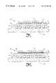
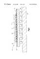
- a second set of solder balls 28is attached to the contacts 26 beneath the carrier.
- This array of balls 28conventionally referred to as a Ball Grid Array or BGA, connect contacts 26 to contacts 34 on a printed circuit board, card or other substrate 32 .
- the solder in the BGA balls 28may be selected to melt at a lower temperature than the solder in the C4 balls 16 , so that chip and carrier can be attached to substrate 32 without disturbing the C4 connections.
Landscapes
- Engineering & Computer Science (AREA)
- Physics & Mathematics (AREA)
- Condensed Matter Physics & Semiconductors (AREA)
- General Physics & Mathematics (AREA)
- Computer Hardware Design (AREA)
- Microelectronics & Electronic Packaging (AREA)
- Power Engineering (AREA)
- Manufacturing & Machinery (AREA)
- Wire Bonding (AREA)
- Structures Or Materials For Encapsulating Or Coating Semiconductor Devices Or Solid State Devices (AREA)
- Non-Metallic Protective Coatings For Printed Circuits (AREA)
Abstract
Description
Claims (15)
Priority Applications (4)
| Application Number | Priority Date | Filing Date | Title |
|---|---|---|---|
| US09/067,708US6191952B1 (en) | 1998-04-28 | 1998-04-28 | Compliant surface layer for flip-chip electronic packages and method for forming same |
| MYPI99001137AMY138376A (en) | 1998-04-28 | 1999-03-25 | Compliant surface layer for flip-chip electronic packages and method for forming same |
| CNB991043901ACN1168138C (en) | 1998-04-28 | 1999-03-26 | Flip-chip electronic package, manufacturing method, and electronic device using the package |
| SG9901579ASG92634A1 (en) | 1998-04-28 | 1999-03-31 | Compliant surface layer for flip-chip electronic packages and method for forming same |
Applications Claiming Priority (1)
| Application Number | Priority Date | Filing Date | Title |
|---|---|---|---|
| US09/067,708US6191952B1 (en) | 1998-04-28 | 1998-04-28 | Compliant surface layer for flip-chip electronic packages and method for forming same |
Publications (1)
| Publication Number | Publication Date |
|---|---|
| US6191952B1true US6191952B1 (en) | 2001-02-20 |
Family
ID=22077843
Family Applications (1)
| Application Number | Title | Priority Date | Filing Date |
|---|---|---|---|
| US09/067,708Expired - LifetimeUS6191952B1 (en) | 1998-04-28 | 1998-04-28 | Compliant surface layer for flip-chip electronic packages and method for forming same |
Country Status (4)
| Country | Link |
|---|---|
| US (1) | US6191952B1 (en) |
| CN (1) | CN1168138C (en) |
| MY (1) | MY138376A (en) |
| SG (1) | SG92634A1 (en) |
Cited By (30)
| Publication number | Priority date | Publication date | Assignee | Title |
|---|---|---|---|---|
| US6309908B1 (en)* | 1999-12-21 | 2001-10-30 | Motorola, Inc. | Package for an electronic component and a method of making it |
| US6362437B1 (en)* | 1999-06-17 | 2002-03-26 | Nec Corporation | Mounting structure of integrated circuit device having high effect of buffering stress and high reliability of connection by solder, and method of mounting the same |
| US6373125B1 (en)* | 2000-02-23 | 2002-04-16 | International Business Machines Corporation | Chip scale package with direct attachment of chip to lead frame |
| US6399896B1 (en)* | 2000-03-15 | 2002-06-04 | International Business Machines Corporation | Circuit package having low modulus, conformal mounting pads |
| US6444921B1 (en)* | 2000-02-03 | 2002-09-03 | Fujitsu Limited | Reduced stress and zero stress interposers for integrated-circuit chips, multichip substrates, and the like |
| US20030045028A1 (en)* | 2001-09-05 | 2003-03-06 | Taiwan Semiconductor Manufacturing Co., Ltd. | Method for stress reduction in flip chip bump during flip chip mounting and underfill process steps of making a microelectronic assembly |
| US20030049888A1 (en)* | 2001-09-11 | 2003-03-13 | Fujitsu Limited | Semiconductor device and method of making the same |
| US20030052414A1 (en)* | 2001-09-14 | 2003-03-20 | Cowens Marvin W. | Adhesion by plasma conditioning of semiconductor chip surfaces |
| US20030116860A1 (en)* | 2001-12-21 | 2003-06-26 | Biju Chandran | Semiconductor package with low resistance package-to-die interconnect scheme for reduced die stresses |
| US6603916B1 (en) | 2001-07-26 | 2003-08-05 | Lightwave Microsystems Corporation | Lightwave circuit assembly having low deformation balanced sandwich substrate |
| SG97872A1 (en)* | 2000-03-23 | 2003-08-20 | Advanpack Solutions Pte Ltd | Method of packaging an integrated circuit device |
| US20030219588A1 (en)* | 2002-04-03 | 2003-11-27 | Makoto Ogawa | Dielectric film for printed wiring board, multilayer printed board, and semiconductor device |
| US6737295B2 (en)* | 2001-02-27 | 2004-05-18 | Chippac, Inc. | Chip scale package with flip chip interconnect |
| US20040106291A1 (en)* | 2001-05-03 | 2004-06-03 | Siliconware Precision Industries Co., Ltd. | Thermally enhanced wafer-level chip scale package and method of fabricating the same |
| US6774315B1 (en)* | 2000-05-24 | 2004-08-10 | International Business Machines Corporation | Floating interposer |
| US6816385B1 (en)* | 2000-11-16 | 2004-11-09 | International Business Machines Corporation | Compliant laminate connector |
| US6849953B2 (en)* | 1998-02-03 | 2005-02-01 | Tessera, Inc. | Microelectronic assemblies with composite conductive elements |
| US20060163717A1 (en)* | 2004-08-03 | 2006-07-27 | Harry Hedler | Method for connection of an integrated circuit to a substrate, and a corresponding circuit arrangement |
| US20070132089A1 (en)* | 2005-12-13 | 2007-06-14 | Tongbi Jiang | Microelectronic devices and methods for manufacturing microelectronic devices |
| US7235886B1 (en)* | 2001-12-21 | 2007-06-26 | Intel Corporation | Chip-join process to reduce elongation mismatch between the adherents and semiconductor package made thereby |
| US20080128885A1 (en)* | 2006-11-30 | 2008-06-05 | Taiwan Semiconductor Manufacturing Co., Ltd. | Stress decoupling structures for flip-chip assembly |
| US20080142996A1 (en)* | 2006-12-19 | 2008-06-19 | Gopalakrishnan Subramanian | Controlling flow of underfill using polymer coating and resulting devices |
| US20080157352A1 (en)* | 2006-12-28 | 2008-07-03 | Shripad Gokhale | Reducing underfill keep out zone on substrate used in electronic device processing |
| US20090179333A1 (en)* | 2008-01-11 | 2009-07-16 | Alfred Martin | Solder contacts and methods of forming same |
| US20090261480A1 (en)* | 2008-04-18 | 2009-10-22 | Alfred Martin | Integrated circuit and method of fabricating the same |
| US20120299201A1 (en)* | 2011-05-25 | 2012-11-29 | International Business Machines Corporation | Use of a Local Constraint to Enhance Attachment of an IC Device to a Mounting Platform |
| CN102820282A (en)* | 2011-06-09 | 2012-12-12 | 奥普蒂兹公司 | 3D integration microelectronic assembly for integrated circuit devices and method of making same |
| US9281238B2 (en)* | 2014-07-11 | 2016-03-08 | United Microelectronics Corp. | Method for fabricating interlayer dielectric layer |
| US20170216947A1 (en)* | 2014-07-28 | 2017-08-03 | Xin Yang | Systems and methods for reinforced adhesive bonding |
| WO2020252161A1 (en) | 2019-06-11 | 2020-12-17 | Uniqarta, Inc. | Material for positional error compensation in assembly of discrete components |
Families Citing this family (8)
| Publication number | Priority date | Publication date | Assignee | Title |
|---|---|---|---|---|
| DE502004010904D1 (en)* | 2004-01-27 | 2010-04-29 | Mettler Toledo Ag | Moisture protection strain gauges with inhomogeneous inorganic layer on smoothing polymer layer (ORMOCER) and slot arrangement |
| CN100356534C (en)* | 2004-06-15 | 2007-12-19 | 日月光半导体制造股份有限公司 | Semiconductor package structure and manufacturing method thereof |
| US7851916B2 (en)* | 2005-03-17 | 2010-12-14 | Taiwan Semiconductor Manufacturing Co., Ltd. | Strain silicon wafer with a crystal orientation (100) in flip chip BGA package |
| US7170159B1 (en)* | 2005-07-07 | 2007-01-30 | Taiwan Semiconductor Manufacturing Company, Ltd. | Low CTE substrates for use with low-k flip-chip package devices |
| CN101814444B (en)* | 2009-04-30 | 2012-01-25 | 中国空空导弹研究院 | Low-stress bottom filling method of laminating device |
| CN102279942A (en)* | 2011-07-25 | 2011-12-14 | 上海祯显电子科技有限公司 | Novel intelligent card |
| EP2748771A1 (en)* | 2011-08-26 | 2014-07-02 | Identive Group, Inc. | Card lamination |
| US20150064851A1 (en)* | 2013-09-03 | 2015-03-05 | Rohm And Haas Electronic Materials Llc | Pre-applied underfill |
Citations (29)
| Publication number | Priority date | Publication date | Assignee | Title |
|---|---|---|---|---|
| US4658332A (en) | 1983-04-04 | 1987-04-14 | Raytheon Company | Compliant layer printed circuit board |
| US4740414A (en) | 1986-11-17 | 1988-04-26 | Rockwell International Corporation | Ceramic/organic multilayer interconnection board |
| US4847146A (en)* | 1988-03-21 | 1989-07-11 | Hughes Aircraft Company | Process for fabricating compliant layer board with selectively isolated solder pads |
| US4847136A (en)* | 1988-03-21 | 1989-07-11 | Hughes Aircraft Company | Thermal expansion mismatch forgivable printed wiring board for ceramic leadless chip carrier |
| US4855872A (en)* | 1987-08-13 | 1989-08-08 | General Electric Company | Leadless ceramic chip carrier printed wiring board adapter |
| US4873615A (en) | 1986-10-09 | 1989-10-10 | Amp Incorporated | Semiconductor chip carrier system |
| US5026624A (en) | 1989-03-03 | 1991-06-25 | International Business Machines Corporation | Composition for photo imaging |
| US5110867A (en)* | 1989-09-15 | 1992-05-05 | Akzo Nv | Interpenetrating polymer network of epoxy resin, polyallyl polymer and anhydride |
| US5258648A (en) | 1991-06-27 | 1993-11-02 | Motorola, Inc. | Composite flip chip semiconductor device with an interposer having test contacts formed along its periphery |
| US5262280A (en) | 1992-04-02 | 1993-11-16 | Shipley Company Inc. | Radiation sensitive compositions |
| US5278010A (en) | 1989-03-03 | 1994-01-11 | International Business Machines Corporation | Composition for photo imaging |
| US5304457A (en) | 1989-03-03 | 1994-04-19 | International Business Machines Corporation | Composition for photo imaging |
| US5329423A (en)* | 1993-04-13 | 1994-07-12 | Scholz Kenneth D | Compressive bump-and-socket interconnection scheme for integrated circuits |
| US5391435A (en)* | 1989-08-15 | 1995-02-21 | Akzo Nobel N.V. | Interpenetrating network of ring-containing allyl polymers and epoxy resin laminate |
| US5439766A (en) | 1988-12-30 | 1995-08-08 | International Business Machines Corporation | Composition for photo imaging |
| US5439779A (en) | 1993-02-22 | 1995-08-08 | International Business Machines Corporation | Aqueous soldermask |
| US5473119A (en) | 1993-02-05 | 1995-12-05 | W. L. Gore & Associates, Inc. | Stress-resistant circuit board |
| US5493075A (en) | 1994-09-30 | 1996-02-20 | International Business Machines Corporation | Fine pitch solder formation on printed circuit board process and product |
| US5496769A (en) | 1993-04-30 | 1996-03-05 | Commissariat A L'energie Atomique | Process for coating electronic components hybridized by bumps on a substrate |
| US5511306A (en) | 1994-04-05 | 1996-04-30 | Compaq Computer Corporation | Masking of circuit board vias to reduce heat-induced board and chip carrier package warp during wavesolder process |
| US5535101A (en) | 1992-11-03 | 1996-07-09 | Motorola, Inc. | Leadless integrated circuit package |
| US5579573A (en) | 1994-10-11 | 1996-12-03 | Ford Motor Company | Method for fabricating an undercoated chip electrically interconnected to a substrate |
| US5633535A (en) | 1995-01-27 | 1997-05-27 | Chao; Clinton C. | Spacing control in electronic device assemblies |
| US5801446A (en)* | 1995-03-28 | 1998-09-01 | Tessera, Inc. | Microelectronic connections with solid core joining units |
| US5808874A (en)* | 1996-05-02 | 1998-09-15 | Tessera, Inc. | Microelectronic connections with liquid conductive elements |
| US5821305A (en)* | 1994-09-08 | 1998-10-13 | Akzo Nobel Nv | Allyl-containing epoxy resin composition comprising a copolymer of an ethylenically unsaturated anhydride and a vinyl compound |
| US5866952A (en)* | 1995-11-30 | 1999-02-02 | Lockheed Martin Corporation | High density interconnected circuit module with a compliant layer as part of a stress-reducing molded substrate |
| US6002590A (en)* | 1998-03-24 | 1999-12-14 | Micron Technology, Inc. | Flexible trace surface circuit board and method for making flexible trace surface circuit board |
| US6054250A (en)* | 1997-02-18 | 2000-04-25 | Alliedsignal Inc. | High temperature performance polymers for stereolithography |
- 1998
- 1998-04-28USUS09/067,708patent/US6191952B1/ennot_activeExpired - Lifetime
- 1999
- 1999-03-25MYMYPI99001137Apatent/MY138376A/enunknown
- 1999-03-26CNCNB991043901Apatent/CN1168138C/ennot_activeExpired - Lifetime
- 1999-03-31SGSG9901579Apatent/SG92634A1/enunknown
Patent Citations (29)
| Publication number | Priority date | Publication date | Assignee | Title |
|---|---|---|---|---|
| US4658332A (en) | 1983-04-04 | 1987-04-14 | Raytheon Company | Compliant layer printed circuit board |
| US4873615A (en) | 1986-10-09 | 1989-10-10 | Amp Incorporated | Semiconductor chip carrier system |
| US4740414A (en) | 1986-11-17 | 1988-04-26 | Rockwell International Corporation | Ceramic/organic multilayer interconnection board |
| US4855872A (en)* | 1987-08-13 | 1989-08-08 | General Electric Company | Leadless ceramic chip carrier printed wiring board adapter |
| US4847146A (en)* | 1988-03-21 | 1989-07-11 | Hughes Aircraft Company | Process for fabricating compliant layer board with selectively isolated solder pads |
| US4847136A (en)* | 1988-03-21 | 1989-07-11 | Hughes Aircraft Company | Thermal expansion mismatch forgivable printed wiring board for ceramic leadless chip carrier |
| US5439766A (en) | 1988-12-30 | 1995-08-08 | International Business Machines Corporation | Composition for photo imaging |
| US5304457A (en) | 1989-03-03 | 1994-04-19 | International Business Machines Corporation | Composition for photo imaging |
| US5026624A (en) | 1989-03-03 | 1991-06-25 | International Business Machines Corporation | Composition for photo imaging |
| US5278010A (en) | 1989-03-03 | 1994-01-11 | International Business Machines Corporation | Composition for photo imaging |
| US5391435A (en)* | 1989-08-15 | 1995-02-21 | Akzo Nobel N.V. | Interpenetrating network of ring-containing allyl polymers and epoxy resin laminate |
| US5110867A (en)* | 1989-09-15 | 1992-05-05 | Akzo Nv | Interpenetrating polymer network of epoxy resin, polyallyl polymer and anhydride |
| US5258648A (en) | 1991-06-27 | 1993-11-02 | Motorola, Inc. | Composite flip chip semiconductor device with an interposer having test contacts formed along its periphery |
| US5262280A (en) | 1992-04-02 | 1993-11-16 | Shipley Company Inc. | Radiation sensitive compositions |
| US5535101A (en) | 1992-11-03 | 1996-07-09 | Motorola, Inc. | Leadless integrated circuit package |
| US5473119A (en) | 1993-02-05 | 1995-12-05 | W. L. Gore & Associates, Inc. | Stress-resistant circuit board |
| US5439779A (en) | 1993-02-22 | 1995-08-08 | International Business Machines Corporation | Aqueous soldermask |
| US5329423A (en)* | 1993-04-13 | 1994-07-12 | Scholz Kenneth D | Compressive bump-and-socket interconnection scheme for integrated circuits |
| US5496769A (en) | 1993-04-30 | 1996-03-05 | Commissariat A L'energie Atomique | Process for coating electronic components hybridized by bumps on a substrate |
| US5511306A (en) | 1994-04-05 | 1996-04-30 | Compaq Computer Corporation | Masking of circuit board vias to reduce heat-induced board and chip carrier package warp during wavesolder process |
| US5821305A (en)* | 1994-09-08 | 1998-10-13 | Akzo Nobel Nv | Allyl-containing epoxy resin composition comprising a copolymer of an ethylenically unsaturated anhydride and a vinyl compound |
| US5493075A (en) | 1994-09-30 | 1996-02-20 | International Business Machines Corporation | Fine pitch solder formation on printed circuit board process and product |
| US5579573A (en) | 1994-10-11 | 1996-12-03 | Ford Motor Company | Method for fabricating an undercoated chip electrically interconnected to a substrate |
| US5633535A (en) | 1995-01-27 | 1997-05-27 | Chao; Clinton C. | Spacing control in electronic device assemblies |
| US5801446A (en)* | 1995-03-28 | 1998-09-01 | Tessera, Inc. | Microelectronic connections with solid core joining units |
| US5866952A (en)* | 1995-11-30 | 1999-02-02 | Lockheed Martin Corporation | High density interconnected circuit module with a compliant layer as part of a stress-reducing molded substrate |
| US5808874A (en)* | 1996-05-02 | 1998-09-15 | Tessera, Inc. | Microelectronic connections with liquid conductive elements |
| US6054250A (en)* | 1997-02-18 | 2000-04-25 | Alliedsignal Inc. | High temperature performance polymers for stereolithography |
| US6002590A (en)* | 1998-03-24 | 1999-12-14 | Micron Technology, Inc. | Flexible trace surface circuit board and method for making flexible trace surface circuit board |
Non-Patent Citations (4)
| Title |
|---|
| IBM Technical Disclosure Bulletin, "Elastic Thermal Compensation of Chip Carriers", v.40, No. 4, pp. 85-86 (Disclosure Text including indication of Apr. 1, 1997 publishing date).* |
| IBM Technical Disclosure Bulletin, pp. 85-86, vol. 40 No. 4, Apr. 1997 Elastic Thermal Compensation of Chip Carriers. |
| U.S. application No. 09/067,707, Susko et al, filed Apr. 28, 1998; for Methods and Apparatus for Balancing Differences in Thermal Expansion in Electronic Packaging. |
| U.S. application No. 09/080,117, Caletka et al., filed May 15, 1998; for Thermally Enhanced and Mechanically Balanced Flip Chip Package and Method of Forming. |
Cited By (64)
| Publication number | Priority date | Publication date | Assignee | Title |
|---|---|---|---|---|
| US6849953B2 (en)* | 1998-02-03 | 2005-02-01 | Tessera, Inc. | Microelectronic assemblies with composite conductive elements |
| US6362437B1 (en)* | 1999-06-17 | 2002-03-26 | Nec Corporation | Mounting structure of integrated circuit device having high effect of buffering stress and high reliability of connection by solder, and method of mounting the same |
| US6309908B1 (en)* | 1999-12-21 | 2001-10-30 | Motorola, Inc. | Package for an electronic component and a method of making it |
| US6444921B1 (en)* | 2000-02-03 | 2002-09-03 | Fujitsu Limited | Reduced stress and zero stress interposers for integrated-circuit chips, multichip substrates, and the like |
| US6373125B1 (en)* | 2000-02-23 | 2002-04-16 | International Business Machines Corporation | Chip scale package with direct attachment of chip to lead frame |
| US6399896B1 (en)* | 2000-03-15 | 2002-06-04 | International Business Machines Corporation | Circuit package having low modulus, conformal mounting pads |
| SG97872A1 (en)* | 2000-03-23 | 2003-08-20 | Advanpack Solutions Pte Ltd | Method of packaging an integrated circuit device |
| US6774315B1 (en)* | 2000-05-24 | 2004-08-10 | International Business Machines Corporation | Floating interposer |
| US6816385B1 (en)* | 2000-11-16 | 2004-11-09 | International Business Machines Corporation | Compliant laminate connector |
| US6737295B2 (en)* | 2001-02-27 | 2004-05-18 | Chippac, Inc. | Chip scale package with flip chip interconnect |
| US20040222440A1 (en)* | 2001-02-27 | 2004-11-11 | Chippac, Inc | Chip scale package with flip chip interconnect |
| US20040106291A1 (en)* | 2001-05-03 | 2004-06-03 | Siliconware Precision Industries Co., Ltd. | Thermally enhanced wafer-level chip scale package and method of fabricating the same |
| US6603916B1 (en) | 2001-07-26 | 2003-08-05 | Lightwave Microsystems Corporation | Lightwave circuit assembly having low deformation balanced sandwich substrate |
| US7015066B2 (en)* | 2001-09-05 | 2006-03-21 | Taiwan Semiconductor Manufacturing Co., Ltd. | Method for stress reduction in flip chip bump during flip chip mounting and underfill process steps of making a microelectronic assembly |
| US20030045028A1 (en)* | 2001-09-05 | 2003-03-06 | Taiwan Semiconductor Manufacturing Co., Ltd. | Method for stress reduction in flip chip bump during flip chip mounting and underfill process steps of making a microelectronic assembly |
| US20050110169A1 (en)* | 2001-09-11 | 2005-05-26 | Fujitsu Limited | Semiconductor device and method of making the same |
| US6869822B2 (en)* | 2001-09-11 | 2005-03-22 | Fujitsu Limited | Method of making a semiconductor device with adhesive sealing subjected to two-fold hardening |
| US20030049888A1 (en)* | 2001-09-11 | 2003-03-13 | Fujitsu Limited | Semiconductor device and method of making the same |
| US7276401B2 (en) | 2001-09-14 | 2007-10-02 | Texas Instruments Incorporated | Adhesion by plasma conditioning of semiconductor chip surfaces |
| US7271494B2 (en) | 2001-09-14 | 2007-09-18 | Texas Instruments Incorporated | Adhesion by plasma conditioning of semiconductor chip surfaces |
| US20080050860A1 (en)* | 2001-09-14 | 2008-02-28 | Cowens Marvin W | Adhesion by plasma conditioning of semiconductor chip |
| US7319275B2 (en) | 2001-09-14 | 2008-01-15 | Texas Instruments Incorporated | Adhesion by plasma conditioning of semiconductor chip |
| US20030052414A1 (en)* | 2001-09-14 | 2003-03-20 | Cowens Marvin W. | Adhesion by plasma conditioning of semiconductor chip surfaces |
| US20050161834A1 (en)* | 2001-09-14 | 2005-07-28 | Cowens Marvin W. | Adhesion by plasma conditioning of semiconductor chip |
| US20050212149A1 (en)* | 2001-09-14 | 2005-09-29 | Cowens Marvin W | Adhesion by plasma conditioning of semiconductor chip surfaces |
| US7445960B2 (en) | 2001-09-14 | 2008-11-04 | Texas Instruments Incorporated | Adhesion by plasma conditioning of semiconductor chip |
| US6869831B2 (en)* | 2001-09-14 | 2005-03-22 | Texas Instruments Incorporated | Adhesion by plasma conditioning of semiconductor chip surfaces |
| US20070128881A1 (en)* | 2001-09-14 | 2007-06-07 | Cowens Marvin W | Adhesion by plasma conditioning of semiconductor chip surfaces |
| US7122403B2 (en) | 2001-12-21 | 2006-10-17 | Intel Corporation | Method of interconnecting die and substrate |
| CN100431396C (en)* | 2001-12-21 | 2008-11-05 | 英特尔公司 | Chip bonding process to reduce elongation mismatch between adherends and semiconductor package fabricated thereby |
| US7235886B1 (en)* | 2001-12-21 | 2007-06-26 | Intel Corporation | Chip-join process to reduce elongation mismatch between the adherents and semiconductor package made thereby |
| US20030116860A1 (en)* | 2001-12-21 | 2003-06-26 | Biju Chandran | Semiconductor package with low resistance package-to-die interconnect scheme for reduced die stresses |
| US20050116329A1 (en)* | 2001-12-21 | 2005-06-02 | Intel Corporation | Semiconductor package with low resistance package-to-die interconnect scheme for reduced die stresses |
| US20030219588A1 (en)* | 2002-04-03 | 2003-11-27 | Makoto Ogawa | Dielectric film for printed wiring board, multilayer printed board, and semiconductor device |
| US6849934B2 (en)* | 2002-04-03 | 2005-02-01 | Japan Gore-Tex, Inc. | Dielectric film for printed wiring board, multilayer printed board, and semiconductor device |
| US20060163717A1 (en)* | 2004-08-03 | 2006-07-27 | Harry Hedler | Method for connection of an integrated circuit to a substrate, and a corresponding circuit arrangement |
| US7517727B2 (en)* | 2004-08-03 | 2009-04-14 | Infineon Technologies Ag | Method for connection of an integrated circuit to a substrate, and a corresponding circuit arrangement |
| US20070132089A1 (en)* | 2005-12-13 | 2007-06-14 | Tongbi Jiang | Microelectronic devices and methods for manufacturing microelectronic devices |
| US7888188B2 (en) | 2005-12-13 | 2011-02-15 | Micron Technology, Inc. | Method of fabicating a microelectronic die having a curved surface |
| US7633157B2 (en)* | 2005-12-13 | 2009-12-15 | Micron Technology, Inc. | Microelectronic devices having a curved surface and methods for manufacturing the same |
| US20100062571A1 (en)* | 2005-12-13 | 2010-03-11 | Micron Technology, Inc. | Microelectronic devices and methods for manufacturing microelectronic devices |
| US20080128885A1 (en)* | 2006-11-30 | 2008-06-05 | Taiwan Semiconductor Manufacturing Co., Ltd. | Stress decoupling structures for flip-chip assembly |
| US7573138B2 (en) | 2006-11-30 | 2009-08-11 | Taiwan Semiconductor Manufacturing Co., Ltd. | Stress decoupling structures for flip-chip assembly |
| US20080142996A1 (en)* | 2006-12-19 | 2008-06-19 | Gopalakrishnan Subramanian | Controlling flow of underfill using polymer coating and resulting devices |
| US20080157352A1 (en)* | 2006-12-28 | 2008-07-03 | Shripad Gokhale | Reducing underfill keep out zone on substrate used in electronic device processing |
| US8362627B2 (en)* | 2006-12-28 | 2013-01-29 | Intel Corporation | Reducing underfill keep out zone on substrate used in electronic device processing |
| US20110084388A1 (en)* | 2006-12-28 | 2011-04-14 | Shripad Gokhale | Reducing underfill keep out zone on substrate used in electronic device processing |
| US7875503B2 (en)* | 2006-12-28 | 2011-01-25 | Intel Corporation | Reducing underfill keep out zone on substrate used in electronic device processing |
| US20090179333A1 (en)* | 2008-01-11 | 2009-07-16 | Alfred Martin | Solder contacts and methods of forming same |
| US7745321B2 (en) | 2008-01-11 | 2010-06-29 | Qimonda Ag | Solder contacts and methods of forming same |
| US20090261480A1 (en)* | 2008-04-18 | 2009-10-22 | Alfred Martin | Integrated circuit and method of fabricating the same |
| US7973417B2 (en) | 2008-04-18 | 2011-07-05 | Qimonda Ag | Integrated circuit and method of fabricating the same |
| US20120299201A1 (en)* | 2011-05-25 | 2012-11-29 | International Business Machines Corporation | Use of a Local Constraint to Enhance Attachment of an IC Device to a Mounting Platform |
| US8432034B2 (en)* | 2011-05-25 | 2013-04-30 | International Business Machines Corporation | Use of a local constraint to enhance attachment of an IC device to a mounting platform |
| CN102820282A (en)* | 2011-06-09 | 2012-12-12 | 奥普蒂兹公司 | 3D integration microelectronic assembly for integrated circuit devices and method of making same |
| US20120313207A1 (en)* | 2011-06-09 | 2012-12-13 | Vage Oganesian | 3D Integration Microelectronic Assembly For Integrated Circuit Devices And Method Of Making Same |
| US8546900B2 (en)* | 2011-06-09 | 2013-10-01 | Optiz, Inc. | 3D integration microelectronic assembly for integrated circuit devices |
| US9054013B2 (en)* | 2011-06-09 | 2015-06-09 | Optiz, Inc. | Method of making 3D integration microelectronic assembly for integrated circuit devices |
| US9281238B2 (en)* | 2014-07-11 | 2016-03-08 | United Microelectronics Corp. | Method for fabricating interlayer dielectric layer |
| US9564507B2 (en) | 2014-07-11 | 2017-02-07 | United Microelectronics Corp. | Interlayer dielectric layer with two tensile dielectric layers |
| US20170216947A1 (en)* | 2014-07-28 | 2017-08-03 | Xin Yang | Systems and methods for reinforced adhesive bonding |
| WO2020252161A1 (en) | 2019-06-11 | 2020-12-17 | Uniqarta, Inc. | Material for positional error compensation in assembly of discrete components |
| EP3984059A4 (en)* | 2019-06-11 | 2022-07-20 | Kulicke & Soffa Netherlands B.V. | MATERIAL FOR POSITION ERROR COMPENSATION IN THE ASSEMBLY OF DISCREET COMPONENTS |
| US12046504B2 (en) | 2019-06-11 | 2024-07-23 | Kulicke & Soffa Netherlands B.V. | Positional error compensation in assembly of discrete components by adjustment of optical system characteristics |
Also Published As
| Publication number | Publication date |
|---|---|
| CN1168138C (en) | 2004-09-22 |
| SG92634A1 (en) | 2002-11-19 |
| CN1244728A (en) | 2000-02-16 |
| MY138376A (en) | 2009-05-29 |
Similar Documents
| Publication | Publication Date | Title |
|---|---|---|
| US6191952B1 (en) | Compliant surface layer for flip-chip electronic packages and method for forming same | |
| US6569711B1 (en) | Methods and apparatus for balancing differences in thermal expansion in electronic packaging | |
| US6224711B1 (en) | Assembly process for flip chip package having a low stress chip and resulting structure | |
| US7026706B2 (en) | Method and packaging structure for optimizing warpage of flip chip organic packages | |
| US6949404B1 (en) | Flip chip package with warpage control | |
| US6562662B2 (en) | Electronic package with bonded structure and method of making | |
| US6667557B2 (en) | Method of forming an apparatus to reduce thermal fatigue stress on flip chip solder connections | |
| US7566834B2 (en) | Wiring board and semiconductor package using the same | |
| US6949415B2 (en) | Module with adhesively attached heat sink | |
| US6909176B1 (en) | Structure and material for assembling a low-K Si die to achieve a low warpage and industrial grade reliability flip chip package with organic substrate | |
| US7573138B2 (en) | Stress decoupling structures for flip-chip assembly | |
| US7224048B1 (en) | Flip chip ball grid array package | |
| US8071881B2 (en) | Wiring board, method for manufacturing same and semiconductor device | |
| US7300822B2 (en) | Low warpage flip chip package solution-channel heat spreader | |
| KR101054239B1 (en) | Underfill Membrane for Printed Wiring Assemblies | |
| US6956165B1 (en) | Underfill for maximum flip chip package reliability | |
| US7504718B2 (en) | Apparatus and methods for constructing balanced chip packages to reduce thermally induced mechanical strain | |
| US7498198B2 (en) | Structure and method for stress reduction in flip chip microelectronic packages using underfill materials with spatially varying properties | |
| US6943060B1 (en) | Method for fabricating integrated circuit package with solder bumps | |
| US6806119B2 (en) | Method of balanced coefficient of thermal expansion for flip chip ball grid array | |
| US20060118947A1 (en) | Thermal expansion compensating flip chip ball grid array package structure | |
| HK1023221A (en) | Compliant surface layer for flip-chip electronic packages and method for forming same | |
| JPH11121525A (en) | Semiconductor device | |
| US20060043602A1 (en) | Flip chip ball grid array package with constraint plate |
Legal Events
| Date | Code | Title | Description |
|---|---|---|---|
| AS | Assignment | Owner name:INTERNATIONAL BUSINESS MACHINES CORPORATION, NEW Y Free format text:ASSIGNMENT OF ASSIGNORS INTEREST;ASSIGNORS:JIMAREZ, MIGUEL A.;JOHNSON, ERIC A.;LI, LI;AND OTHERS;REEL/FRAME:009303/0980;SIGNING DATES FROM 19980608 TO 19980626 | |
| FEPP | Fee payment procedure | Free format text:PAYOR NUMBER ASSIGNED (ORIGINAL EVENT CODE: ASPN); ENTITY STATUS OF PATENT OWNER: LARGE ENTITY | |
| STCF | Information on status: patent grant | Free format text:PATENTED CASE | |
| FPAY | Fee payment | Year of fee payment:4 | |
| FPAY | Fee payment | Year of fee payment:8 | |
| REMI | Maintenance fee reminder mailed | ||
| FPAY | Fee payment | Year of fee payment:12 | |
| SULP | Surcharge for late payment | Year of fee payment:11 | |
| AS | Assignment | Owner name:GLOBALFOUNDRIES U.S. 2 LLC, NEW YORK Free format text:ASSIGNMENT OF ASSIGNORS INTEREST;ASSIGNOR:INTERNATIONAL BUSINESS MACHINES CORPORATION;REEL/FRAME:036550/0001 Effective date:20150629 | |
| AS | Assignment | Owner name:GLOBALFOUNDRIES INC., CAYMAN ISLANDS Free format text:ASSIGNMENT OF ASSIGNORS INTEREST;ASSIGNORS:GLOBALFOUNDRIES U.S. 2 LLC;GLOBALFOUNDRIES U.S. INC.;REEL/FRAME:036779/0001 Effective date:20150910 | |
| AS | Assignment | Owner name:GLOBALFOUNDRIES U.S. INC., NEW YORK Free format text:RELEASE BY SECURED PARTY;ASSIGNOR:WILMINGTON TRUST, NATIONAL ASSOCIATION;REEL/FRAME:056987/0001 Effective date:20201117 |