US6191750B1 - Traveling wave slot antenna and method of making same - Google Patents
Traveling wave slot antenna and method of making sameDownload PDFInfo
- Publication number
- US6191750B1 US6191750B1US09/262,163US26216399AUS6191750B1US 6191750 B1US6191750 B1US 6191750B1US 26216399 AUS26216399 AUS 26216399AUS 6191750 B1US6191750 B1US 6191750B1
- Authority
- US
- United States
- Prior art keywords
- traveling wave
- stripline
- conductor sheet
- low profile
- slot antenna
- Prior art date
- Legal status (The legal status is an assumption and is not a legal conclusion. Google has not performed a legal analysis and makes no representation as to the accuracy of the status listed.)
- Expired - Lifetime
Links
- 238000004519manufacturing processMethods0.000titleclaimsdescription7
- 239000004020conductorSubstances0.000claimsabstractdescription67
- 238000000034methodMethods0.000claimsdescription13
- 230000005540biological transmissionEffects0.000claimsdescription10
- 238000000576coating methodMethods0.000claimsdescription2
- 239000003989dielectric materialSubstances0.000claims1
- 230000007704transitionEffects0.000abstractdescription12
- 239000000463materialSubstances0.000description7
- 125000006850spacer groupChemical group0.000description7
- 238000013461designMethods0.000description4
- 230000008569processEffects0.000description3
- 239000000758substrateSubstances0.000description3
- 230000008859changeEffects0.000description2
- 238000005516engineering processMethods0.000description2
- 238000000206photolithographyMethods0.000description2
- 230000005855radiationEffects0.000description2
- 239000000853adhesiveSubstances0.000description1
- 230000001070adhesive effectEffects0.000description1
- 238000003491arrayMethods0.000description1
- 238000004891communicationMethods0.000description1
- 230000000295complement effectEffects0.000description1
- 238000011161developmentMethods0.000description1
- 230000005684electric fieldEffects0.000description1
- 230000005672electromagnetic fieldEffects0.000description1
- 239000000945fillerSubstances0.000description1
- 238000009434installationMethods0.000description1
- 238000012986modificationMethods0.000description1
- 230000004048modificationEffects0.000description1
- 230000010287polarizationEffects0.000description1
- 230000000750progressive effectEffects0.000description1
- 230000001902propagating effectEffects0.000description1
- 238000011160researchMethods0.000description1
- 230000004044responseEffects0.000description1
- 238000007493shaping processMethods0.000description1
Images


Classifications
- H—ELECTRICITY
- H01—ELECTRIC ELEMENTS
- H01Q—ANTENNAS, i.e. RADIO AERIALS
- H01Q13/00—Waveguide horns or mouths; Slot antennas; Leaky-waveguide antennas; Equivalent structures causing radiation along the transmission path of a guided wave
- H01Q13/20—Non-resonant leaky-waveguide or transmission-line antennas; Equivalent structures causing radiation along the transmission path of a guided wave
- H01Q13/206—Microstrip transmission line antennas
- H—ELECTRICITY
- H01—ELECTRIC ELEMENTS
- H01Q—ANTENNAS, i.e. RADIO AERIALS
- H01Q1/00—Details of, or arrangements associated with, antennas
- H01Q1/36—Structural form of radiating elements, e.g. cone, spiral, umbrella; Particular materials used therewith
- H01Q1/38—Structural form of radiating elements, e.g. cone, spiral, umbrella; Particular materials used therewith formed by a conductive layer on an insulating support
- H—ELECTRICITY
- H01—ELECTRIC ELEMENTS
- H01Q—ANTENNAS, i.e. RADIO AERIALS
- H01Q13/00—Waveguide horns or mouths; Slot antennas; Leaky-waveguide antennas; Equivalent structures causing radiation along the transmission path of a guided wave
- H01Q13/08—Radiating ends of two-conductor microwave transmission lines, e.g. of coaxial lines, of microstrip lines
- H01Q13/085—Slot-line radiating ends
Definitions
- the present inventionrelates to a traveling wave slot antenna and a method of making it.
- the inventionmore particularly relates to a traveling wave slot antenna, which has a broad frequency band width and which has a low profile configuration to enable it to be mounted, for example, in the outer skin of aircraft as well as many other applications.
- Printed circuit antennaehave been known as narrow band elements since the 1960's. Elements making up such an antenna usually take the form of a planar structure with a conductive plate suspended above a ground plane fed at one or more feed points. See, for example, U.S. Pat. No. 5,748,152, which is incorporated herein by reference.
- antennashave been used in many applications with wide variations in characteristics.
- such an antennais intended to radiate normal to the ground plane surface to which they are mounted.
- the antenna elementsare commonly fabricated using photolithography techniques on printed circuit board materials. Such techniques allow for very accurate reproduction of the elements in large quantities. These antenna are easily combined into arrays for use at microwave frequencies for communication, Radar and sensing applications.
- the U.S. Pat. No. 5,748,152discloses a slot notch antenna which is generally planar in configuration and has a pair of diverging slot sections terminating in an aperture.
- the planar antennais positioned within an open top enclosure above a flat base ground plane. Such a configuration is inherently lossy, and thus not sufficiently efficient for many applications.
- Another object of the present inventionis to provide such a new and improved antenna and method wherein the method enables the antenna to be manufactured at a relatively low cost.
- a further object of the present inventionis to provide such an antenna having an element which can be configured as a totally conformal aperture as a single element or in an array.
- a still further object of the present inventionis to provide a conformal antenna that requires a very small volume to achieve its efficient broadband performance.
- a yet another object of the present inventionis to provide an antenna which can be fabricated with materials and processes that are low cost while sufficiently accurate to enable high yield production of phased matched array elements.
- Another object of the present inventionis to provide an antenna which can be realized using high temperature dielectric and adhesives for high temperature environments.
- a traveling wave slot antennawhich is made by printed circuit board techniques and materials in a three-dimensional configuration.
- a novel low profile non-resonant traveling wave slot antenna operating over broad frequency bandsis in the form of a multiple layer circuit, which includes a generally planar slotted conductor sheet having an open smoothly curved tapered planar slot therein and a three-dimensionally smoothly curved conductor sheet having an elongated stem portion fixedly electrically connected at its distal end to a feed point on top of the slotted conductor sheet and extending downwardly through the slot therein and terminating in an enlarged smoothly tapered portion to transition the characteristic impedance between the feed point and an aperture having an impedance of free space.
- the novel antennais a novel combination of microwave transmission line technology, slot antenna concepts, resistive materials and processes and printed circuit fabrication techniques.
- the inventionrelates to the manner this novel design enables the antenna designer to meet desired electrical performance parameters.
- the inventive antenna designfacilitates the following design parameters: Frequency bandwidth, Polarization, Gain, aperture efficiency, other electrical requirements and size, all of which are critical to desired design performance.
- the novel antennais a traveling wave slot which can be accurately constructed using printed circuit materials and processes.
- itis a coaxial transmission line to stripline transmission line transition that then transitions through a covered microstrip region to a covered coplanar waveguide to feed a broadband terminated di-electrically loaded slot aperture.
- the coaxial cable to stripline transitionhas an intrinsically broadband frequency response and is realized using conventional components.
- the novel transition from stripline transmission line to covered microstrip to covered co-planar waveguideis achieved through a combination of tapering the surface of the three dimensionally curved stripline conductor member and shaping the slotted planar member of the circuit board layers.
- the electric field created across the slot apertureis very well behaved over a great frequency bandwidth and can be configured to radiate efficiently in a low profile or totally conformal installation.
- FIG. 1is a partially broken away pictorial view of a low profile traveling wave slot antenna, which is constructed in accordance with the present invention and illustrates the front, left side and bottom of the antenna;
- FIG. 2is a partially broken away pictorial sectional view taken substantially on line 2 — 2 of FIG. 2;
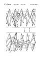
- FIGS. 3 through 9are diagrammatic views illustrating an electromagnet traveling wave signal propagating through the antenna of FIG. 1 wherein the characteristic impedance transitions between a feed point and an aperture of the antenna;
- FIG. 10is a bottom view of the antenna of FIG. 1;
- FIG. 11is an exploded pictorial view of the principal components of the antenna of FIG. 1, illustrating the top, rear and right sides thereof;
- FIG. 12is similar to FIG. 11 and is an exploded pictorial view of the components of the antenna of FIG. 1, illustrating the front, bottom and left sides thereof;
- FIGS. 13-17are reduced scale face views of the top sides of the components of FIGS. 11 and 12;
- FIGS. 18-22are reduced scale face views of the bottom sides of the components of FIGS. 11 and 12, the stripline conductor element shown in FIGS. 14 and 19 being an illustration of it in its flat configuration prior to assembly into the antenna of FIGS. 1-12.
- FIG. 23is a pictorial sectional view of the antenna of FIG. 10 taken substantially on line 23 — 23 thereof.
- the antenna 10is a non-resonant antenna which operates over broad frequency bands, and can be surface mounted or otherwise used in a conformal application.
- the antenna 10can be integrated into a vehicle skin or housing (not shown), as well as many other commercial applications including, but not limited to, any application where a small, compact light-weight broad band antenna may be utilized.
- the antenna 10is constructed by utilizing printed circuit technologies in a multiple layer circuit arrangement.
- the antenna 10has a low height compact boxlike rectangular assembly of generally rectangular stacked or layered elements.
- An upright coaxial feed point connector 12 at the rear end of the antenna 10conveys electromagnetic signals, which propagate to and from the antenna 10 and transition through progressive sections of smoothly varying impedance characteristics between the connector 12 and a broad band terminated di-electrically loaded slot aperture generally indicated at 14 , where the impedance is substantially matched to free space, to enable radiating or receiving electromagnetic wave signals.
- a generally planar slotted or notched conductor element 16forms one layer of the antenna 10 and has a generally rectangular planar corresponding slotted or notched conductor sheet 17 (FIGS. 12 and 20) underlying a generally rectangular substrate 19 of the element 16 .
- An open smoothly curved tapered planar generally V-shaped slot 18is disposed in the conductor element 16 , which receives a three dimensionally smoothly curved complementary shaped stripline conductor element 23 (FIGS.
- the stripline conductor element 23includes an elongated stem portion 27 fixedly and electrically connected at its rear distal end at 29 to a center conductor 28 of the coaxial connector 12 (FIGS. 3 and 11 ), whereby an outer conductor generally indicated at 30 (FIGS. 3 and 11) is electrically and fixedly connected to the conductor sheet 17 on the underside thereof.
- the conductor element 23includes an enlarged generally triangularly shaped, smoothly tapered portion 32 which extends curvilinearly downwardly from the rear elongated stem portion 27 through the tapered open slot 18 in the planar conductor sheet 17 to help define at its front distal end 34 (FIG. 11) the aperture 14 together with a generally planar imperforate rectangular conductor top plate 36 of a top layer or element 39 having a substrate 40 .
- the downwardly curved stripline conductor sheet 25cooperates with the slotted planar conductor sheet 17 having the tapered slot 18 , as well as the top ground plane flat conductor plate 36 , to provide a smooth characteristic impedance change between the coaxial connector 12 and the aperture 14 .
- the electromagnetic signal in the coaxial connector 12is generally radial, as indicated, and may have an impedance of near 50 ohms. As shown in FIG.
- the signalprogresses through an impedance change to greater than 50 ohms through a stripline transmission line section configuration including the rectilinear stem portion 27 of the stripline curved conductor 25 being disposed above and parallel to the planar conductor 17 and the ground conductor plate 36 .
- the stem portion 27extends above the slot 18 in the conductor sheet 17 to further transition continuously and uninterruptedly the stripline to a higher impedance.
- the curved conductor sheet 25cooperates with the planar conductor sheet 17 and the ground plate 36 to enter a covered microstrip section as indicated in FIG. 6, whereby the electromagnetic field extends substantially entirely between the curved conductor sheet 25 and the ground plane plate 36 .
- the impedanceincreases to greater than 0 ohms.
- the stem 27 of the sheet 25enters the slot 18 , and is co-planar with the planar conductor 17 .
- the traveling wavespropogate through a co-planar wave guide section since the stem 27 of the curved sheet 25 is disposed within the slot 18 to help confine the electromagnetic traveling waves between the co-planar sheets 17 and 25 and the spaced apart top conductor plate 36 .
- the impedanceincreases to near that of free space.
- a further transition of the curved sheet 25 at its enlarged portion 32is disposed below the planar sheet 17 opposite the slot 18 .
- the traveling waveextends entirely between the distal end 34 of the curved plate 25 , and the top conductor plate 36 , since the slot 18 of the conductor sheet 17 is no longer present.
- the impedanceis still higher.
- the impedancematched to about 377 ohms which would be the impedance of free space.
- a generally planar upright imperforate rectangular conductor back plate 38interconnects electrically the top ground plate 36 and a generally planar imperforate rectangular conductor base or bottom plate 41 .
- a pair of upright resistive coatings or films 43 and 45 on opposite sides of the antenna 10help impedance match the element of the low end of its operating frequency band.
- a dielectric filler material 47(FIGS. 1 and 2) disposed above the sheet 25 help confine the traveling waves within the antenna 10 .
- a set of three notched spacer plates 49 , 52 and 54are mounted below the member 16 to help position the curved sheet 25 as indicated in the drawings.
- a set of four vertically aligned mounting holes, such as the set of vertically aligned mounting holes 56 extending through the rear end portion of the antenna 10secure the various layers in position, it being understood that the fastening devices are not shown for sake of illustration purposes.
- a set of mounting holes, such as the hole 58 in the distal end 34 of the stripline curved conductor element 23enables the distal end 34 to be secured in place and provides for an electrical contact to the vehicle surface to which it is mounted.
- the spacer plates 49 , 52 and 54have at their respective rear end portions mounting holes 61 , 63 and 65 for the connector 12 , which includes an apertured flange 67 received within the rectangular holes 61 and 63 .
- the slot 18is generally V-shaped and is preferably formed by a pair of smoothly rounded inwardly curved slit openings 72 and 74 .
- the strip line conductor element 23is integrally connected at its stemportion 27 to the remaining portion of the element 16 .
- the conductor sheet 25is formed as a conductor layer on the substrate 19 .
- the stripline curved conductor element 23includes a pair of smoothly rounded outwardly flared intermediate edge portions 76 and 78 interconnecting the elongated stem portion 27 and the enlarged portion 32 .
- a pair of gently outwardly curved side edges 81 and 83 of the enlarged tapered portion 32is smoothly continues with the respective intermediate edge portions 76 and 78 .
- a bottom conductor strip 84(FIGS. 12 and 24) is connected integrally over the distal end 34 with the conductor sheet 25 .
- the plate 49is a layer disposed immediately below the element 16 .
- the plate 49includes a generally V-shaped slot or notch 85 , which is generally similar in size and shape as the slot 21 and which is axially aligned therewith.
- the spacer plate 52 as shown in FIGS. 16 and 21is disposed immediately below the plate 49 and includes a moderately shallow slot or notch 87 , which is similar in size and shape as a portion of the slot 85 .
- the slot 87includes a bight portion 89 interconnecting a pair of smoothly rounded inwardly curved leg portions 92 and 94 similar to corresponding portions of the respective leg portions of the slot 85 of the spacer plate 49 .
- the slot 87is axially aligned with the deeper slot 85 . Due to the shallowness of the slot 87 , the bight 89 is substantially longer than the light of the slot 85 .
- the spacer plate 54(FIGS. 17 and 22) is disposed below the plate 52 , and includes a shallow slot or notch 96 , which is similar in size and shape as the slot 87 and is axially aligned therewith.
- the slot 96includes a bight portion 98 , which is substantially longer than the bight portion 89 of the slot 87 .
- the progressively more shallow spacer slotsare axially aligned to receive the downwardly extending stripline conductor element 23 to position precisely the downwardly curvilinear disposition and support it intermediate its ends 29 and 34 which are fixed in place.
- the antenna 10is preferable made by printed circuit photolithography techniques on printed circuit board materials.
Landscapes
- Waveguide Aerials (AREA)
Abstract
Description
Claims (15)
Priority Applications (1)
| Application Number | Priority Date | Filing Date | Title |
|---|---|---|---|
| US09/262,163US6191750B1 (en) | 1999-03-03 | 1999-03-03 | Traveling wave slot antenna and method of making same |
Applications Claiming Priority (1)
| Application Number | Priority Date | Filing Date | Title |
|---|---|---|---|
| US09/262,163US6191750B1 (en) | 1999-03-03 | 1999-03-03 | Traveling wave slot antenna and method of making same |
Publications (1)
| Publication Number | Publication Date |
|---|---|
| US6191750B1true US6191750B1 (en) | 2001-02-20 |
Family
ID=22996419
Family Applications (1)
| Application Number | Title | Priority Date | Filing Date |
|---|---|---|---|
| US09/262,163Expired - LifetimeUS6191750B1 (en) | 1999-03-03 | 1999-03-03 | Traveling wave slot antenna and method of making same |
Country Status (1)
| Country | Link |
|---|---|
| US (1) | US6191750B1 (en) |
Cited By (17)
| Publication number | Priority date | Publication date | Assignee | Title |
|---|---|---|---|---|
| US6407711B1 (en) | 2001-04-24 | 2002-06-18 | Science And Applied Technology, Inc. | Antenna array apparatus with conformal mounting structure |
| US6724345B2 (en)* | 2002-04-22 | 2004-04-20 | Kyocera Wirless Corp. | Antenna with periodic electromagnetic mode suppression structures and method for same |
| US20040150579A1 (en)* | 2001-04-26 | 2004-08-05 | Dotto Kim V. | Ultra-wideband antennas |
| US20050078043A1 (en)* | 2003-10-14 | 2005-04-14 | Apostolos John T. | Gapless concatenated vivaldi notch/meander line loaded antennas |
| US20070024511A1 (en)* | 2005-07-27 | 2007-02-01 | Agc Automotive Americas R&D, Inc. | Compact circularly-polarized patch antenna |
| US20070216589A1 (en)* | 2006-03-16 | 2007-09-20 | Agc Automotive Americas R&D | Multiple-layer patch antenna |
| US20110026237A1 (en)* | 2009-01-05 | 2011-02-03 | Raytheon Company | Multi-purpose mounting devices for mounting electrical packages to airborne objects |
| CN102136626A (en)* | 2010-11-23 | 2011-07-27 | 南京邮电大学 | Broadband-narrowband combined antenna |
| WO2014047567A1 (en)* | 2012-09-21 | 2014-03-27 | Wireless Research Development | Dual polarization antenna |
| US20140306854A1 (en)* | 2012-06-30 | 2014-10-16 | Javier Ruben Flores-Cuadras | Vivaldi-monopole antenna |
| US8976513B2 (en) | 2002-10-22 | 2015-03-10 | Jason A. Sullivan | Systems and methods for providing a robust computer processing unit |
| US9450309B2 (en) | 2013-05-30 | 2016-09-20 | Xi3 | Lobe antenna |
| US9478867B2 (en) | 2011-02-08 | 2016-10-25 | Xi3 | High gain frequency step horn antenna |
| US9478868B2 (en) | 2011-02-09 | 2016-10-25 | Xi3 | Corrugated horn antenna with enhanced frequency range |
| US9606577B2 (en) | 2002-10-22 | 2017-03-28 | Atd Ventures Llc | Systems and methods for providing a dynamically modular processing unit |
| US9961788B2 (en) | 2002-10-22 | 2018-05-01 | Atd Ventures, Llc | Non-peripherals processing control module having improved heat dissipating properties |
| US20230143858A1 (en)* | 2021-11-09 | 2023-05-11 | Pctel, Inc. | Thin metal vivaldi antenna systems |
Citations (6)
| Publication number | Priority date | Publication date | Assignee | Title |
|---|---|---|---|---|
| US5081466A (en)* | 1990-05-04 | 1992-01-14 | Motorola, Inc. | Tapered notch antenna |
| US5194875A (en)* | 1991-06-07 | 1993-03-16 | Westinghouse Electric Corp. | Notch radiator elements |
| US5404146A (en)* | 1992-07-20 | 1995-04-04 | Trw Inc. | High-gain broadband V-shaped slot antenna |
| US5428364A (en)* | 1993-05-20 | 1995-06-27 | Hughes Aircraft Company | Wide band dipole radiating element with a slot line feed having a Klopfenstein impedance taper |
| US5748152A (en)* | 1994-12-27 | 1998-05-05 | Mcdonnell Douglas Corporation | Broad band parallel plate antenna |
| US5949382A (en)* | 1990-09-28 | 1999-09-07 | Raytheon Company | Dielectric flare notch radiator with separate transmit and receive ports |
- 1999
- 1999-03-03USUS09/262,163patent/US6191750B1/ennot_activeExpired - Lifetime
Patent Citations (6)
| Publication number | Priority date | Publication date | Assignee | Title |
|---|---|---|---|---|
| US5081466A (en)* | 1990-05-04 | 1992-01-14 | Motorola, Inc. | Tapered notch antenna |
| US5949382A (en)* | 1990-09-28 | 1999-09-07 | Raytheon Company | Dielectric flare notch radiator with separate transmit and receive ports |
| US5194875A (en)* | 1991-06-07 | 1993-03-16 | Westinghouse Electric Corp. | Notch radiator elements |
| US5404146A (en)* | 1992-07-20 | 1995-04-04 | Trw Inc. | High-gain broadband V-shaped slot antenna |
| US5428364A (en)* | 1993-05-20 | 1995-06-27 | Hughes Aircraft Company | Wide band dipole radiating element with a slot line feed having a Klopfenstein impedance taper |
| US5748152A (en)* | 1994-12-27 | 1998-05-05 | Mcdonnell Douglas Corporation | Broad band parallel plate antenna |
Cited By (29)
| Publication number | Priority date | Publication date | Assignee | Title |
|---|---|---|---|---|
| US6407711B1 (en) | 2001-04-24 | 2002-06-18 | Science And Applied Technology, Inc. | Antenna array apparatus with conformal mounting structure |
| US20040150579A1 (en)* | 2001-04-26 | 2004-08-05 | Dotto Kim V. | Ultra-wideband antennas |
| US6911951B2 (en)* | 2001-04-26 | 2005-06-28 | The University Of British Columbia | Ultra-wideband antennas |
| US6724345B2 (en)* | 2002-04-22 | 2004-04-20 | Kyocera Wirless Corp. | Antenna with periodic electromagnetic mode suppression structures and method for same |
| US10285293B2 (en) | 2002-10-22 | 2019-05-07 | Atd Ventures, Llc | Systems and methods for providing a robust computer processing unit |
| US9961788B2 (en) | 2002-10-22 | 2018-05-01 | Atd Ventures, Llc | Non-peripherals processing control module having improved heat dissipating properties |
| US9606577B2 (en) | 2002-10-22 | 2017-03-28 | Atd Ventures Llc | Systems and methods for providing a dynamically modular processing unit |
| US10849245B2 (en) | 2002-10-22 | 2020-11-24 | Atd Ventures, Llc | Systems and methods for providing a robust computer processing unit |
| US11751350B2 (en) | 2002-10-22 | 2023-09-05 | Atd Ventures, Llc | Systems and methods for providing a robust computer processing unit |
| US8976513B2 (en) | 2002-10-22 | 2015-03-10 | Jason A. Sullivan | Systems and methods for providing a robust computer processing unit |
| US20050078043A1 (en)* | 2003-10-14 | 2005-04-14 | Apostolos John T. | Gapless concatenated vivaldi notch/meander line loaded antennas |
| US6882322B1 (en)* | 2003-10-14 | 2005-04-19 | Bae Systems Information And Electronic Systems Integration Inc. | Gapless concatenated Vivaldi notch/meander line loaded antennas |
| US20070024511A1 (en)* | 2005-07-27 | 2007-02-01 | Agc Automotive Americas R&D, Inc. | Compact circularly-polarized patch antenna |
| US7333059B2 (en) | 2005-07-27 | 2008-02-19 | Agc Automotive Americas R&D, Inc. | Compact circularly-polarized patch antenna |
| US7545333B2 (en) | 2006-03-16 | 2009-06-09 | Agc Automotive Americas R&D | Multiple-layer patch antenna |
| US20070216589A1 (en)* | 2006-03-16 | 2007-09-20 | Agc Automotive Americas R&D | Multiple-layer patch antenna |
| US8559191B2 (en)* | 2009-01-05 | 2013-10-15 | Raytheon Company | Multi-purpose mounting devices for mounting electrical packages to airborne objects |
| US20110026237A1 (en)* | 2009-01-05 | 2011-02-03 | Raytheon Company | Multi-purpose mounting devices for mounting electrical packages to airborne objects |
| CN102136626B (en)* | 2010-11-23 | 2013-10-30 | 南京邮电大学 | Broadband-narrowband combined antenna |
| CN102136626A (en)* | 2010-11-23 | 2011-07-27 | 南京邮电大学 | Broadband-narrowband combined antenna |
| US9478867B2 (en) | 2011-02-08 | 2016-10-25 | Xi3 | High gain frequency step horn antenna |
| US9478868B2 (en) | 2011-02-09 | 2016-10-25 | Xi3 | Corrugated horn antenna with enhanced frequency range |
| US20140306854A1 (en)* | 2012-06-30 | 2014-10-16 | Javier Ruben Flores-Cuadras | Vivaldi-monopole antenna |
| US9257747B2 (en)* | 2012-06-30 | 2016-02-09 | Taoglas Group Holdings Limited | Vivaldi-monopole antenna |
| WO2014047567A1 (en)* | 2012-09-21 | 2014-03-27 | Wireless Research Development | Dual polarization antenna |
| US20160380359A1 (en)* | 2012-09-21 | 2016-12-29 | Henry Cooper | Dual polarization antenna |
| US9450309B2 (en) | 2013-05-30 | 2016-09-20 | Xi3 | Lobe antenna |
| US20230143858A1 (en)* | 2021-11-09 | 2023-05-11 | Pctel, Inc. | Thin metal vivaldi antenna systems |
| US11855345B2 (en)* | 2021-11-09 | 2023-12-26 | Pctel, Inc. | Thin metal Vivaldi antenna systems |
Similar Documents
| Publication | Publication Date | Title |
|---|---|---|
| US6191750B1 (en) | Traveling wave slot antenna and method of making same | |
| US4197545A (en) | Stripline slot antenna | |
| US4853704A (en) | Notch antenna with microstrip feed | |
| US5070340A (en) | Broadband microstrip-fed antenna | |
| US4843403A (en) | Broadband notch antenna | |
| US4931808A (en) | Embedded surface wave antenna | |
| US6133879A (en) | Multifrequency microstrip antenna and a device including said antenna | |
| EP0873577B1 (en) | Slot spiral antenna with integrated balun and feed | |
| US4063246A (en) | Coplanar stripline antenna | |
| US4125839A (en) | Dual diagonally fed electric microstrip dipole antennas | |
| US7026993B2 (en) | Planar antenna and array antenna | |
| US4320402A (en) | Multiple ring microstrip antenna | |
| US4675685A (en) | Low VSWR, flush-mounted, adaptive array antenna | |
| US6271799B1 (en) | Antenna horn and associated methods | |
| US4843400A (en) | Aperture coupled circular polarization antenna | |
| US8232924B2 (en) | Broadband patch antenna and antenna system | |
| US4329689A (en) | Microstrip antenna structure having stacked microstrip elements | |
| JPH11284430A (en) | Short-circuit antenna manufactured by microstrip technology and device including the antenna | |
| US5319378A (en) | Multi-band microstrip antenna | |
| US20130044037A1 (en) | Circuitry-isolated mems antennas: devices and enabling technology | |
| US5568159A (en) | Flared notch slot antenna | |
| US20200287297A1 (en) | Dual-polarized substrate-integrated beam steering antenna | |
| US20130241787A1 (en) | Modular gridded tapered slot antenna | |
| US5467099A (en) | Resonated notch antenna | |
| US6567047B2 (en) | Multi-band in-series antenna assembly |
Legal Events
| Date | Code | Title | Description |
|---|---|---|---|
| STCF | Information on status: patent grant | Free format text:PATENTED CASE | |
| FEPP | Fee payment procedure | Free format text:PAYOR NUMBER ASSIGNED (ORIGINAL EVENT CODE: ASPN); ENTITY STATUS OF PATENT OWNER: LARGE ENTITY | |
| FEPP | Fee payment procedure | Free format text:PAT HOLDER NO LONGER CLAIMS SMALL ENTITY STATUS, ENTITY STATUS SET TO UNDISCOUNTED (ORIGINAL EVENT CODE: STOL); ENTITY STATUS OF PATENT OWNER: LARGE ENTITY | |
| REFU | Refund | Free format text:REFUND - SURCHARGE, PETITION TO ACCEPT PYMT AFTER EXP, UNINTENTIONAL (ORIGINAL EVENT CODE: R2551); ENTITY STATUS OF PATENT OWNER: LARGE ENTITY | |
| AS | Assignment | Owner name:BANK OF AMERICA, N.A., NORTH CAROLINA Free format text:SECURITY INTEREST;ASSIGNORS:ALLIANT TECHSYSTEMS INC.;ALLANT AMMUNITION AND POWDER COMPANY LLC;ALLIANT AMMUNITION SYSTEMS COMPANY LLC;AND OTHERS;REEL/FRAME:014692/0653 Effective date:20040331 | |
| FPAY | Fee payment | Year of fee payment:4 | |
| FEPP | Fee payment procedure | Free format text:ENTITY STATUS SET TO UNDISCOUNTED (ORIGINAL EVENT CODE: BIG.); ENTITY STATUS OF PATENT OWNER: LARGE ENTITY | |
| AS | Assignment | Owner name:ATK SPACE SYSTEMS INC., CALIFORNIA Free format text:MERGER;ASSIGNOR:COMPOSITE OPTICS, INCORPORATED;REEL/FRAME:020709/0911 Effective date:20060322 | |
| AS | Assignment | Owner name:ALLIANT TECHSYSTEMS INC., MINNESOTA Free format text:ASSIGNMENT OF ASSIGNORS INTEREST;ASSIGNOR:ATK SPACE SYSTEMS INC.;REEL/FRAME:020723/0452 Effective date:20080331 | |
| FPAY | Fee payment | Year of fee payment:8 | |
| AS | Assignment | Owner name:BANK OF AMERICA, N.A., CALIFORNIA Free format text:SECURITY AGREEMENT;ASSIGNORS:ALLIANT TECHSYSTEMS INC.;AMMUNITION ACCESSORIES INC.;ATK COMMERCIAL AMMUNITION COMPANY INC.;AND OTHERS;REEL/FRAME:025321/0291 Effective date:20101007 | |
| FPAY | Fee payment | Year of fee payment:12 | |
| AS | Assignment | Owner name:BANK OF AMERICA, N.A., CALIFORNIA Free format text:SECURITY AGREEMENT;ASSIGNORS:ALLIANT TECHSYSTEMS INC.;CALIBER COMPANY;EAGLE INDUSTRIES UNLIMITED, INC.;AND OTHERS;REEL/FRAME:031731/0281 Effective date:20131101 | |
| AS | Assignment | Owner name:WELLS FARGO BANK, NATIONAL ASSOCIATION, AS ADMINISTRATIVE AGENT, NORTH CAROLINA Free format text:SECURITY AGREEMENT;ASSIGNORS:ORBITAL ATK, INC.;ORBITAL SCIENCES CORPORATION;REEL/FRAME:036732/0170 Effective date:20150929 Owner name:WELLS FARGO BANK, NATIONAL ASSOCIATION, AS ADMINIS Free format text:SECURITY AGREEMENT;ASSIGNORS:ORBITAL ATK, INC.;ORBITAL SCIENCES CORPORATION;REEL/FRAME:036732/0170 Effective date:20150929 | |
| AS | Assignment | Owner name:ORBITAL ATK, INC. (F/K/A ALLIANT TECHSYSTEMS INC.) Free format text:RELEASE BY SECURED PARTY;ASSIGNOR:BANK OF AMERICA, N.A.;REEL/FRAME:036815/0330 Effective date:20150929 Owner name:ALLIANT TECHSYSTEMS INC., VIRGINIA Free format text:RELEASE BY SECURED PARTY;ASSIGNOR:BANK OF AMERICA, N.A.;REEL/FRAME:036815/0330 Effective date:20150929 Owner name:COMPOSITE OPTICS, INC., CALIFORNIA Free format text:RELEASE BY SECURED PARTY;ASSIGNOR:BANK OF AMERICA, N.A.;REEL/FRAME:036815/0330 Effective date:20150929 Owner name:FEDERAL CARTRIDGE CO., MINNESOTA Free format text:RELEASE BY SECURED PARTY;ASSIGNOR:BANK OF AMERICA, N.A.;REEL/FRAME:036815/0330 Effective date:20150929 | |
| AS | Assignment | Owner name:ORBITAL ATK, INC. (F/K/A ALLIANT TECHSYSTEMS INC.), VIRGINIA Free format text:RELEASE BY SECURED PARTY;ASSIGNOR:BANK OF AMERICA, N.A.;REEL/FRAME:036816/0624 Effective date:20150929 Owner name:EAGLE INDUSTRIES UNLIMITED, INC., MISSOURI Free format text:RELEASE BY SECURED PARTY;ASSIGNOR:BANK OF AMERICA, N.A.;REEL/FRAME:036816/0624 Effective date:20150929 Owner name:ALLIANT TECHSYSTEMS INC., VIRGINIA Free format text:RELEASE BY SECURED PARTY;ASSIGNOR:BANK OF AMERICA, N.A.;REEL/FRAME:036816/0624 Effective date:20150929 Owner name:ORBITAL ATK, INC. (F/K/A ALLIANT TECHSYSTEMS INC.) Free format text:RELEASE BY SECURED PARTY;ASSIGNOR:BANK OF AMERICA, N.A.;REEL/FRAME:036816/0624 Effective date:20150929 Owner name:FEDERAL CARTRIDGE CO., MINNESOTA Free format text:RELEASE BY SECURED PARTY;ASSIGNOR:BANK OF AMERICA, N.A.;REEL/FRAME:036816/0624 Effective date:20150929 Owner name:AMMUNITION ACCESSORIES, INC., ALABAMA Free format text:RELEASE BY SECURED PARTY;ASSIGNOR:BANK OF AMERICA, N.A.;REEL/FRAME:036816/0624 Effective date:20150929 | |
| AS | Assignment | Owner name:ORBITAL ATK, INC., MINNESOTA Free format text:CHANGE OF NAME;ASSIGNOR:ALLIANT TECHSYSTEMS INC.;REEL/FRAME:045031/0335 Effective date:20150209 | |
| AS | Assignment | Owner name:ORBITAL ATK, INC., MINNESOTA Free format text:CHANGE OF NAME;ASSIGNOR:ALLIANT TECHSYSTEMS INC.;REEL/FRAME:045130/0205 Effective date:20150209 | |
| AS | Assignment | Owner name:ORBITAL ATK, INC., VIRGINIA Free format text:TERMINATION AND RELEASE OF SECURITY INTEREST IN PATENTS;ASSIGNOR:WELLS FARGO BANK, NATIONAL ASSOCIATION, AS ADMINISTRATIVE AGENT;REEL/FRAME:046477/0874 Effective date:20180606 |