US6191470B1 - Semiconductor-on-insulator memory cell with buried word and body lines - Google Patents
Semiconductor-on-insulator memory cell with buried word and body linesDownload PDFInfo
- Publication number
- US6191470B1 US6191470B1US08/889,395US88939597AUS6191470B1US 6191470 B1US6191470 B1US 6191470B1US 88939597 AUS88939597 AUS 88939597AUS 6191470 B1US6191470 B1US 6191470B1
- Authority
- US
- United States
- Prior art keywords
- lines
- memory cell
- access
- word
- line
- Prior art date
- Legal status (The legal status is an assumption and is not a legal conclusion. Google has not performed a legal analysis and makes no representation as to the accuracy of the status listed.)
- Expired - Lifetime
Links
Images


Classifications
- H—ELECTRICITY
- H10—SEMICONDUCTOR DEVICES; ELECTRIC SOLID-STATE DEVICES NOT OTHERWISE PROVIDED FOR
- H10B—ELECTRONIC MEMORY DEVICES
- H10B12/00—Dynamic random access memory [DRAM] devices
- H10B12/01—Manufacture or treatment
- H10B12/02—Manufacture or treatment for one transistor one-capacitor [1T-1C] memory cells
- H10B12/05—Making the transistor
- H—ELECTRICITY
- H10—SEMICONDUCTOR DEVICES; ELECTRIC SOLID-STATE DEVICES NOT OTHERWISE PROVIDED FOR
- H10B—ELECTRONIC MEMORY DEVICES
- H10B12/00—Dynamic random access memory [DRAM] devices
- H10B12/30—DRAM devices comprising one-transistor - one-capacitor [1T-1C] memory cells
- H10B12/48—Data lines or contacts therefor
- H10B12/488—Word lines
- H—ELECTRICITY
- H10—SEMICONDUCTOR DEVICES; ELECTRIC SOLID-STATE DEVICES NOT OTHERWISE PROVIDED FOR
- H10B—ELECTRONIC MEMORY DEVICES
- H10B12/00—Dynamic random access memory [DRAM] devices
- H10B12/30—DRAM devices comprising one-transistor - one-capacitor [1T-1C] memory cells
- H10B12/31—DRAM devices comprising one-transistor - one-capacitor [1T-1C] memory cells having a storage electrode stacked over the transistor
- H—ELECTRICITY
- H10—SEMICONDUCTOR DEVICES; ELECTRIC SOLID-STATE DEVICES NOT OTHERWISE PROVIDED FOR
- H10B—ELECTRONIC MEMORY DEVICES
- H10B12/00—Dynamic random access memory [DRAM] devices
- H10B12/30—DRAM devices comprising one-transistor - one-capacitor [1T-1C] memory cells
- H10B12/48—Data lines or contacts therefor
- H10B12/482—Bit lines
- H—ELECTRICITY
- H10—SEMICONDUCTOR DEVICES; ELECTRIC SOLID-STATE DEVICES NOT OTHERWISE PROVIDED FOR
- H10D—INORGANIC ELECTRIC SEMICONDUCTOR DEVICES
- H10D86/00—Integrated devices formed in or on insulating or conducting substrates, e.g. formed in silicon-on-insulator [SOI] substrates or on stainless steel or glass substrates
- H10D86/201—Integrated devices formed in or on insulating or conducting substrates, e.g. formed in silicon-on-insulator [SOI] substrates or on stainless steel or glass substrates the substrates comprising an insulating layer on a semiconductor body, e.g. SOI
Definitions
- the present inventionrelates generally to semiconductor memory devices, and particularly to a dynamic random access memory (DRAM) having a memory cell with buried word and body lines.
- DRAMdynamic random access memory
- Dynamic random access memoriestypically include an array of stacked or deep trench capacitors for storing data as charge.
- Memory cell access field-effect transistorsFETs
- DRAMSthat are fabricated on bulk silicon substrates are susceptible to “soft errors” resulting from alpha particles that stray from the environment or integrated circuit package. Such alpha particles penetrate the bulk silicon substrate, where they generate large numbers of minority charge carriers. These minority charge carriers are collected at reverse-biased pn-junctions of the access FETs, where they perturb the data that is stored as charge on the storage capacitors.
- large trench or stacked storage capacitorsare required in bulk silicon DRAMs in order to store large quantities of charge. These capacitors constitute an estimated 30% of DRAM fabrication cost.
- SOI substratestypically comprise a thin layer of active semiconductor, such as silicon, on an underlying insulating layer, such as silicon dioxide (SiO 2 ). Memory cells are fabricated upon the thin active semiconductor layer. The number of minority charge carriers generated by a penetrating alpha particle decreases along with the available semiconductor volume. Since SOI substrates present less available semiconductor volume than bulk silicon substrates, fewer minority carriers are generated in the thin active semiconductor layer. As a result, SOI DRAMs are less prone to disturbance of data charges resulting from alpha particles.
- storage capacitors in an SOI DRAMcan be an estimated one-tenth the size of storage capacitors in a bulk silicon DRAM. The difference may become even greater as technology advances and dimensions become smaller. Bulk silicon DRAMs will require comparatively larger-valued storage capacitances. Such larger storage capacitances will likely occupy more integrated circuit area or require a high dielectric constant insulating material, thereby increasing fabrication cost and complexity. SOI DRASMs, having smaller-valued storage capacitances, will be cheaper than bulk silicon DRAMs.
- a further considerationis a body bias voltage that is provided to the body portion of the memory cell access FET to improve memory cell operation.
- the body bias voltageallows the memory cell to operate from a low power supply voltage, such as 1.5 volts, from which a gate voltage controlling the access FET is derived. Turning the access FET on to transfer data to or from the storage capacitor requires a gate voltage in excess of a turn-on threshold voltage. However, low power supply voltages, such as 1.5 volts, may not provide sufficient overdrive voltage in excess of the threshold voltage to fully turn on the access FET.
- the gate voltage required for turning on the access FETcan be reduced by controlling the body bias voltage.
- the body bias voltagealso controls a subthreshold leakage current of the access FET.
- the access FETis turned off when data is stored as charge on the storage capacitor.
- the subthreshold leakage currentremoves some of the stored data charges from the storage node of the storage capacitor.
- the body bias voltage valuecontrols the reverse bias of the access FET pn junction that is coupled to the storage node. By increasing the reverse bias of such pn junctions, the subthreshold leakage current is reduced. Without a proper body bias voltage, the subthreshold leakage current would lead to short data retention times.
- Providing the body bias voltage to the memory cell access FETsrequires a conductive body line that interconnects the access FET body contacts to receive the body bias voltage.
- the body line, as well as bit line, word line, and other such conductorsall occupy integrated circuit surface area.
- the surface area of each memory cellreferred to as its “footprint”, must be minimized.
- conventional memory cellstypically require word lines and body lines on the upper surface of the memory cell, requiring surface area in addition to that of the memory cell storage capacitor.
- the present inventionprovides a memory cell.
- a semiconductor islandis formed on a substrate.
- An access transistoris formed in the island, including first and second source/drain regions, a gate region, and a body region.
- a conductive word lineis formed substantially adjacent to the island and located at a height that is no higher than the island's upper surface. The word line is coupled to the gate region of the access transistor.
- a conductive body regionis formed substantially adjacent to a side surface of the island and located at a height that is no higher than the island's upper surface. The body line is coupled to the body region of the access transistor.
- a conductive bit lineis electrically coupled to the first source/drain region of the access transistor.
- a storage capacitoris coupled to the second source/drain region of the access transistor.
- the memory cell arraycomprises a plurality of memory cells.
- Each memory cellincludes an access transistor having a gate region, a body region, and first and second source/drain regions.
- Each memory cellfurther includes a storage capacitor coupled to the second source/drain region of the access transistor.
- a plurality of parallel isolation trenchesincludes first and second trenches alternatingly disposed between rows of the memory cells for providing isolation therebetween.
- a plurality of word linesis provided. Each word line is carried in one of the first trenches at a height that is no higher than the upper surface of the body region of the access transistor. Each word line is coupled to the gate region of access transistors in the row of the memory cells.
- a plurality of body linesis provided.
- Each body lineis carried in one of the second trenches at a height that is no higher than the upper surface of the access transistor.
- Each body lineis coupled to the body region of access transistors in at least one row of the memory cells.
- a plurality of bit linesis provided. Each bit line is coupled to the first source/drain region of ones of the access transistors.
- the semiconductor memory arrayincludes a dielectric layer carried by a substrate.
- First and second semiconductor barsare formed on the dielectric layer.
- Each of the barsincludes a plurality of active areas.
- An electrically isolating dielectric materialis interposed between adjacent ones of the active areas.
- a plurality of access transistorsis provided, including an access transistor formed in each of the active areas of the bars.
- a plurality of isolation trenchesis provided, including a trench located between the first and second bars and extending approximately the length of the bar.
- a plurality of word linesis provided, including a word line located in the trench and extending approximately the length of the trench along a first side of the bars.
- a plurality of body linesis provided, including a body line extending approximately along a second side of the first and second bars.
- a plurality of bit linesis also provided.
- the present inventionprovides a semiconductor memory device, including a memory array.
- the memory arrayincludes a plurality of bit lines, a plurality of word lines, and a plurality of memory cells.
- Each memory cellincludes an access transistor having a gate region, a body region, and first and second source/drain regions.
- Each memory cellincludes a storage capacitor that is electrically coupled to the second source/drain region of the access transistor.
- Access circuitryis provided for accessing the memory cells.
- a plurality of isolation trenchesis provided, including a first trench between first and second access transistors and a second trench between the second and third access transistors.
- a first one of the word linesis located in the first trench at a height that is no higher than the upper surface of the access transistor.
- the first word lineis electrically coupled to the gate regions of the first and second access transistors.
- a first one of the body linesis located in the second trench at a height that is no higher than the upper surface of the access transistor.
- the first body lineis electrically coupled to the body portions of the second and third access transistors.
- a first one of the bit linesis coupled to the first source/drain region of each of the first, second and third access transistors.
- Another embodiment of the inventionincludes a method of fabricating a memory array on a semiconductor substrate.
- First and second trenchesare formed in the substrate to define a bar of the semiconductor material.
- An insulating layeris formed between the bar and the substrate for providing electrical isolation therebetween.
- a plurality of active areas of semiconductor materialare defined on the bar.
- An access transistoris produced in each of the active areas.
- Each access transistorincludes gate, body, and first and second source/drain regions.
- a word lineis formed in the first trench. The word line is coupled to the gate region of at least one of the access transistors.
- a body lineis formed in the second trench. The body line is electrically connected to the body portion of at least one of the access transistors.
- Another embodiment of the inventionprovides a method for fabricating a memory array on a semiconductor substrate.
- a plurality of trenchesis formed in the substrate to define at least first, second and third bars of the semiconductor material.
- An insulating layeris formed between the bars and the substrate for providing electrical isolation therebetween.
- a plurality of semiconductor active areasis defined on each of the bars.
- An access transistoris produced in each of the active areas.
- Each access transistorincludes gate, body, and first and second source/drain regions.
- a word lineis formed in a first one of the trenches. The word line is coupled to the gate region of a plurality of the access transistors on the first and second bars.
- a body lineis formed in a second one of the trenches. The body line is electrically coupled to the body region of a plurality of the access transistors on the second and third bars.
- the present inventionprovides a memory device and fabrication method that includes a memory cell having an access FET word lines and body lines that occupy reduced integrated circuit area.
- the inventionalso provides a compact radiation insensitive semiconductor-on-insulator memory cell, which uses a smaller storage capacitor, increases memory data storage density, and reduces integrated circuit manufacturing costs.
- FIG. 1is a schematic representation illustrating generally one embodiment of a semiconductor memory device according to the invention.
- FIG. 2is a plan view illustrating generally a portion of one embodiment of a memory cell array according to the invention.
- FIG. 3is a vertical cross-section view taken along the line 3 — 3 of FIG. 2 .
- FIG. 4is a vertical cross-section view taken along the line 4 — 4 of FIG. 2 .
- FIG. 5is an enlarged plan view illustrating generally one embodiment of the invention, including the memory cell and the sidewall contact between the body line and the body region of the access transistor.
- FIGS. 6A-6Killustrate generally process steps for producing a memory cell in accordance with one embodiment of the invention.
- FIGS. 7A-7Cillustrate generally process steps for producing a memory cell in accordance with another embodiment of the invention.
- wafer and substrateare interchangeably used to refer generally to any structure on which integrated circuits are formed, and also to such structures during various stages of integrated circuit fabrication. Both terms include doped and undoped semiconductors, epitaxial layers of a semiconductor on a supporting semiconductor or insulating material, combinations of such layers, as well as other such structures that are known in the art.
- doped and undoped semiconductorsinclude doped and undoped semiconductors, epitaxial layers of a semiconductor on a supporting semiconductor or insulating material, combinations of such layers, as well as other such structures that are known in the art.
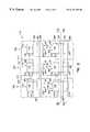
- FIG. 1is a schematic representation illustrating generally one embodiment of a semiconductor memory 100 device incorporating an array of memory cells provided by the invention.
- memory 100illustrates, by way of example but not by way of limitation, a dynamic random access memory (DRAM), but the invention also includes any other semiconductor memory devices.
- Memory 100includes memory cell arrays 110 , such as 110 A and 110 B. Each array 110 includes M rows and N columns of memory cells 112 .
- each memory cellincludes a transfer device, such as n-channel cell access field-effect transistor (FET) 130 or any other known or unknown transistor or switching device.
- Access FET 130is coupled to a storage node of a storage capacitor 132 .
- the other terminal of storage capacitor 132is coupled to a reference voltage such as the ground voltage VSS.
- Each of the M rowsincludes one of word lines WL 0 , WL 1 . . . WLm ⁇ 1, WLm coupled to the input nodes of memory cells 112 at respective gate terminals of access FETs 130 or to the control terminal of an equivalent switching device.
- Each of the M rowsalso includes one of body lines R 1 , R 2 , . . . , Rm ⁇ 1, Rm coupled to the body terminals of access FETs 130 in memory cells 112 .
- Each of the N columnsincludes one of bit lines BL 0 , BL 1 . . . BLn ⁇ 1, BLn.
- Bit lines BL 0 -BLnare used to write to and read data from memory cells 112 .
- Word lines WL 0 -WLmare used to access a particular row of memory cells 112 that is to be written or read.
- Addressing circuitryis also included.
- address buffer 114controls column decoders 118 , which also include sense amplifiers and input/output circuitry that is coupled to bit lines BL 0 -BLn.
- Address buffer 114also controls row decoders 116 .
- Row decoders 116 and column decoders 118selectably access memory cells 112 in response to address signals that are provided on address lines 120 during write and read operations.
- the address signalsare typically provided by an external controller such as a microprocessor or other memory controller.
- Each of memory cells 112has a substantially identical structure, and accordingly, only one memory cell 112 structure is described herein.
- memory 100receives an address of a particular memory cell 112 at address buffer 114 .
- Address buffer 114identifies one of the word lines WL 0 -WLm of the particular memory cell 112 to row decoder 116 .
- Row decoder 116selectively activates the particular word line WL 0 -WLm to activate access FETs 130 of each memory cell 112 that is connected to the selected word line WL 0 -WLm.
- Column decoder 118selects the one of bit lines BL 0 -BLn of the particularly addressed memory cell 112 .
- data received by input/output circuitryis coupled to the one of bit lines BL 0 -BLn and through the access FET 130 to charge or discharge the storage capacitor 132 of the selected memory cell 112 to represent binary data.
- data stored in the selected memory cell 112is coupled to the one of bit lines BL 0 -BLn, amplified, and a corresponding voltage level is provided to the input/output circuits.
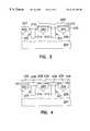
- FIG. 2is a plan view illustrating generally a portion of array 110 including the structure of the memory cells 112 according to the invention.
- memory cells 112are fabricated using semiconductor-on-insulator (SOI) techniques.
- SOIsemiconductor-on-insulator
- a plurality of active semiconductor rows 202are first formed, such as of a silicon material. Rows 202 are separated from an underlying semiconductor substrate by an insulator, such as silicon dioxide (also referred to as “oxide”). After formation, rows 202 are further processed to define isolated active areas of semiconductor, such as silicon islands 203 , which are similarly insulated from the underlying substrate.
- Bit lines 208represent, by way of example, conductive segments of any ones of bit lines BL 0 -BLn.
- Word lines 212which are coupled to gate regions 228 of ones of access FETs 130 , represent, by way of example, conductive segments of any ones of word lines WL 0 -WLm.
- Body lines 214represent, by way of example, conductive segments of any one of body lines R 0 -Rm that interconnect body contacts 232 that are coupled to body regions 217 of access FETs 130 in a particular row of memory cells 112 .
- memory cells 112makes reference to only the six memory cells 112 a-f , to bit lines 208 , word lines 212 , and the body lines 214 that are associated with these memory cells 112 . However, the following description may be similarly applied to other memory cells 112 and conductive lines in ones of arrays 110 .
- each of memory cells 112 a-fincludes an access FET 130 , having a first n+ source/drain region 216 , a p ⁇ body region 217 in which a transistor channel region is formed at the surface, and an second n+ source/drain region 218 .
- a thin gate oxide region 219overlies the channel region that is formed on the upper surface of the body region 217 of access FET 130 .
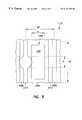
- FIGS. 3 and 4are cross sectional illustrations taken along respective cut lines 3 — 3 and 4 — 4 illustrated in FIG. 2 .
- word line 212is disposed in a trench 221 that extends along one side of a row of silicon islands 203 .
- Body line 214is disposed in a trench 222 that extends, parallel to trench 221 , along the opposite side of the row of silicon islands 203 .
- Word lines 212 and body lines 214are buried below the active semiconductor surface of silicon islands 203 in memory cells 112 .
- Word lines 212 and body lines 214are buried in an insulating layer such as silicon dioxide (oxide) 206 , which electrically isolates adjacent memory cells 112 .
- Each word line 212is shared by pairs of adjacent memory cells 112 , such as memory cell pair 112 b and 112 c and memory cell pair 112 e and 112 f .
- each body line 214is shared by adjacent memory cell pairs, such as memory cell pair 112 a and 112 b and memory cell pair 112 d and 112 e.
- Word lines 212can be formed of a refractory metal, such as tungsten or titanium, or of polysilicon, or other suitable material, depending upon the particular fabrication process used. Word lines 212 are coupled to gate regions 228 that extend outward therefrom to overlie the channel regions of access FETs 130 of adjacent memory cells 112 , such as memory cells 112 e and 112 f and memory cells 112 b and 112 c . Gate regions 228 can be made of polysilicon or other suitable conductive material.
- Body lines 214are coupled to p ⁇ body portions 217 of access FETs 130 in memory cells 112 by extending body contact 232 portions. Body contacts 232 extend through portions of oxide 206 along the sidewalls of trenches 222 . Body lines 214 can be formed of a refractory metal, such as tungsten or titanium, or of polysilicon, or other suitable conductive material depending on the particular fabrication process used. A body bias voltage signal is applied to a body portions 217 of access FETs 130 in a row of memory cells 112 .
- the body bias voltageis synchronously applied through one of body lines R 0 -RM, such as through body line 214 , together with a word line activation signal that is applied to one of word lines WL 0 -WLm, such as to word line 212 , for activating access FETs 130 of the same row of memory cells 112 .
- word line 212is provided approximately 0 Volts.
- body line 214is provided approximately ⁇ 1.5 V to reverse bias the pn junction of the access FET 130 , reduce subthreshold leakage currents, and increase data retention time.
- word line activation signalis applied, word line 212 is provided approximately 1.5 Volts and body line 214 is provided approximately 0.5 Volts in order to decrease the turn-on threshold voltage of the access FET 130 and thereby increase the effective gate overdrive voltage provided on the word line 212 .
- Word line 212controls the gate regions 228 of access FETs 130 on either side of the word line 212 .
- adjacent ones of body lines R 0 -Rm on either side of the word line 212are synchronously activated together with word line 212 , as described above, in order to provide body bias voltages to these same access FETs 130 .
- Access FETs 130 that are formed on silicon islands 203function as transfer devices between ones of bit lines BL 0 -BLn and storage capacitors 132 of corresponding memory cells 112 .
- word lines 212 and body lines 214are vertically oriented, according to one aspect of the invention.
- buried word lines 212 and body lines 214have a surface line width that is less than minimum lithographic feature size F when viewed from above, as shown in FIG. 2 .
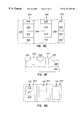
- FIG. 5is a plan view that illustrates generally the very compact memory cell 112 that results.
- each memory cell 112has a pitch width of approximately 2F, measured from the centerline of word line 212 to the centerline of body line 214 , and a pitch length of approximately 4F, where F is the minimum lithographic feature size. F corresponds to the drawn length dimension of access FET 130 . Thus, the surface area of each of memory cells 112 is approximately 8F 2 .
- word line 212 and body line 214are located at or below the active silicon surface 227 of silicon island 203 , but no higher than surface 227 . This advantageously provides additional space on the upper portion of memory cells 112 for formation of storage capacitors 132 , thus increasing the possible storage capacitance value that is available for a given memory cell 112 surface area.
- Signal interconnection contacts to word lines 212 and body lines 214can be made, for example, outside of arrays 110 using conventional etching and contact formation methods.
- bit lines 208extend orthogonally to word lines 212 .
- Bit lines 208overlie intersecting portions of word lines 212 and ones of the source/drain regions 216 of the pair of source/drain regions of the access FET 130 in memory cell 112 .
- Bit lines 208are electrically coupled to ones of the access FET 130 source/drain regions 216 by downwardly extending contact portions 230 of bit lines 208 .
- a storage capacitor 132such as a stacked capacitor, is formed over the other source/drain region 218 of the pair of source/drain regions of the access FET 130 using any of the many capacitor structures and process sequences known in the art
- FIGS. 6A-Killustrate generally structures resulting from steps in one embodiment of a process of making a memory 100 according to the present invention.
- memory cells 112are produced using SOI processing techniques.
- a p-type silicon wafer substrate 204is used as a starting material.
- Substrate 204is processed to form parallel trenches 602 , which define bars or rows 202 of semiconductor material from which active areas of silicon islands 203 are formed.
- silicon islands 203are produced by the method of U.S. patent application, Ser. No. 08/706,230 of Leonard Forbes, entitled “Technique For Producing Small Islands of Silicon On Insulator,” which is assigned to Micron Technology, Inc., and which disclosure is incorporated herein by reference.
- silicon islands 203are formed by the method of U.S. Pat. application, Ser. No. 08/745,708 of Wendell P. Noble, entitled “Technique For Producing Small Islands of Silicon On Insulator,” which also is assigned to Micron Technology, Inc.
- silicon islands 203are formed using local oxidation of silicon (LOCOS), separation by implanted oxygen (SIMOX), or other SOI process technology.
- LOCSlocal oxidation of silicon
- SIMOXseparation by implanted oxygen
- silicon substrate 204is directionally etched to form trenches 602 , leaving rows 202 of silicon protruding upwardly from the substrate 204 , such as shown in FIG. 6 A.
- silicon rows 202have widths of one micron or less between trenches 602 .
- the depth and width of trenches 602can be approximately equal to the width of silicon rows 202 .
- substrate 204is oxidized at a temperature of approximately 900 to 1,100 degrees Celsius, covered with silicon nitride (Si 3 N 4 ), and masked and etched to form exposed oxide regions using standard techniques. Then, the exposed oxide regions are directionally etched, such as by reactive ion etching (RIE), thereby forming trenches 602 in substrate 204 .
- RIEreactive ion etching
- a Si 3 N 4 cap 604is formed on the silicon rows 202 , such as by chemical vapor deposition (CVD).
- Cap 604is formed on rows 202 , overhanging partly down the sidewalls of trenches 602 . Material overhanging the top of trenches 602 prevents cap 604 from covering the lower portions of the sidewalls of trenches 602 .
- some residual Si 3 N 4 606is deposited onto the bottom of trenches 602 .
- a photoresist maskis used to cover rows 202 during etch removal of residual Si 3 N 4 606 on the bottom of trenches 602 .
- An isotropic chemical etchis then used to partially undercut silicon rows 202 , as shown in FIG. 6C.
- a standard chemical etch using hydrofluoric acid (HF) or a commercial etchant sold under the trade name “CP4”(a mixture of approximately 1 part (46% HF): 1 part (CH 3 COOH):3 parts (HNO 3 )) is one example of such an isotropic etchant that can be used.
- HFhydrofluoric acid
- CP4a commercial etchant sold under the trade name “CP4” (a mixture of approximately 1 part (46% HF): 1 part (CH 3 COOH):3 parts (HNO 3 )) is one example of such an isotropic etchant that can be used.
- the volume of silicon removed by this isotropic etchshould correspond to a subsequently formed volume of oxide, as
- Partially undercutting silicon rows 202reduces the effective width of rows 202 between trenches 602 . The resulting distance is small enough that a relatively short, simple oxidation can fully undercut rows 202 . Fully undercutting the rows 202 of silicon during the isotropic etch is also possible because the width of rows 202 is one micron or less.
- Substrate 204is then oxidized using a standard silicon processing furnace at a temperature of approximately 900 to 1,100 degrees Celsius.
- oxide 206isolates silicon rows 202 from silicon substrate 204 .
- a wet, oxidizing ambientis used in the furnace chamber to oxidize the exposed silicon regions on the lower sidewall portions of trenches 602 in a direction that is parallel to the surface of substrate 204 .
- Substrate 204is oxidized for a sufficient time period such that resulting oxide 206 fully undercuts rows 202 , thereby isolating rows 202 from substrate 204 .
- Resulting oxide 206fills the trenches 602 between rows 202 .
- the oxidation time perioddepends on the initial width of rows 202 and the effective width of rows 202 after the partial undercut step. Narrower rows 202 require less oxidation time. For example, for sub-micron technology, the oxidation time is approximately 3 to 4 hours. For sub-0.25 micron technology, oxidation time is approximately 1 hour.
- Silicon islands 203are then defined in the individual silicon rows 202 .
- LOCOS or another such processis used to form oxide 616 between active areas of semiconductor islands, such as silicon islands 203 shown in FIG. 6 E.
- the area of the silicon islands 203is approximately one square micron or less for sub-micron technology and approximately 0.0625 square microns or less for sub-0.25 micron technology.
- Trenches 221 and 222in which a respective word line 212 and body line 214 are to be formed, are vertically etched into oxide 206 between rows of silicon islands 203 , as shown in FIG. 6 F.
- access FETs 130are formed in the silicon islands 203 .
- standard silicon CMOS integrated circuit process technologyis used during these steps to form access FETs 130 .
- gate oxide 219 , gate region 228 , body region 217 , and source/drain regions 216 and 218are formed for each access FET 130 on an individual silicon island 203 .
- buried word line 212 and body line 214are formed in respective trenches 221 and 222 .
- a high-quality thin gate oxide 219is first grown, including over the body region 217 .
- a conductive gate 228such as polysilicon, is formed on the gate oxide 219 , such as by CVD or other technique.
- Gate 228is patterned, such as by RIE, and can later be silicided.
- Source/drain regions 216 and 218are then formed, such as by a low energy phosphorus or arsenic ion implantation having an approximate range of 30-60 KeV and an approximate dose of slightly over 2*10 5 per cm 2 . Resulting source/drain regions 216 and 218 are self-aligned to gate 228 of access FET 130 .
- Body contact openings 630are formed through portions of oxide 206 along the sidewalls of trench 222 for providing electrical contact between body line 214 and the body region 217 of access FET 130 .
- Forming openings 630 between trench 222 and body region 217 of access FET 130includes masking, photoresist, and RIE of oxide 206 , producing the structure shown in FIG. 6H.
- a slight overexposure of the photoresistis made during the photolithography to define oversized openings 630 .
- a slight RIE over etching of oxide 206 on the sidewalls of trenches 222ensures good sidewall contacts to p- body regions 217 of access FETs 130 .
- conductive word lines 212 and body lines 214are formed, such as by CVD depositing a refractory metal (e.g., tungsten) or other suitable material in respective trenches 221 and 222 .
- a refractory metale.g., tungsten
- Body contact 232 portions of the conductive material deposited in trench 222substantially fills openings 630 , providing electrical continuity between body line 214 and the p ⁇ body region 217 of access FET 130 , producing the structure shown in FIG. 61 .
- Word line contacts 640are then formed, such as by depositing and patterning metal or other conductive material between word line 212 and gate 228 , providing the structure as shown in FIG. 6 J.
- FIG. 6 J and FIG. 3are taken along the same cut line 3 — 3 of FIG. 2 .
- Bit lines 208can be formed together with the word line contacts 640 , in which case the resultant structure is shown in FIG. 6 K.
- FIGS. 6K and 4are taken along the same cut line 4 — 4 of FIG. 2 .
- Bit lines 208are formed to contact a source/drain region 216 of a pair of source/drain regions associated with an access FET 130 .
- the remainder of the structure of memory cell 112 thus formedis then processed to fabricate a storage capacitor 132 on the upper surface of each memory cell 112 .
- known stacked capacitor fabrication techniquescan be used, followed by conventional back end of line (BEOL) process procedures.
- FIGS. 7A-Cillustrate generally another embodiment of a method of fabricating memory cell 112 according to the present invention.
- word line 212 and body line 214are formed in respective trenches 221 and 222 prior to forming access FETs 130 in silicon islands 203 .
- silicon islands 203are formed, with isolation trenches 221 and 222 between rows 202 of silicon islands 203 , using the process described above with respect to FIGS. 6A-6F.
- Body contact openings 630are then formed, as shown in FIG. 7A, through oxide 206 to the portion of silicon island 203 from which the p ⁇ body region 217 of the access FET 130 is formed during subsequent process steps.
- word line 212 and body line 214are polysilicon or other suitable conductor formed by low pressure chemical vapor deposition (LPCVD), or other suitable process, then patterned by RIE.
- LPCVDlow pressure chemical vapor deposition
- an n+ polysilicon or other suitable conductoris deposited by CVD to a thickness of 50 nm to form word line 212 and body line 214 as shown in FIG. 7 B.
- Word line 212 and body line 214can be formed together in the same step in respective trenches 221 and 222 , on both sides of a row 202 of silicon islands 203 .
- Word lines 212 and body lines 214can include silicides, such as tungsten silicide formed by CVD.
- Sidewall body contacts 232 in openings 630are formed together with body lines 214 for contacting the body regions 217 of the access FETs 130 in silicon islands 203 . Excess material used in forming word lines 212 and body lines 214 can be removed, such as by chemical mechanical polishing (CMP) or other suitable method.
- CMPchemical mechanical polishing
- access FETs 130are formed in substantially the same manner described above with respect to FIGS. 6D-E, providing the structure shown in FIG. 7 C.
- Subsequent memory cell 112 processingincludes forming the word line contacts 640 as described with respect to FIG. 6J, and producing conductive bit lines 208 , as described above with respect to FIG. 6 K.
- Subsequent processingfurther includes fabricating a storage capacitor 132 on the upper surface of the memory cell 112 , using known techniques, followed by conventional back end of line (BEOL) process procedures.
- BEOLback end of line
- the present inventionprovides arrays of memory cells using SOI techniques in which word lines and body lines are buried in trenches formed on opposite sides of rows of active semiconductor material.
- Each memory cellincludes an access FET coupled to a storage capacitor.
- Word lines and body linesare formed having less than a minimum lithographic feature size F when viewed from the upper surface of the memory cell.
- the memory cell structurehas a surface area of approximately 8F 2 .
- Contact between the body regions of the access FETs and interconnecting body linesis provided through openings in oxide sidewalls of the trenches. This reduces the surface area required by the memory cell.
Landscapes
- Engineering & Computer Science (AREA)
- Manufacturing & Machinery (AREA)
- Semiconductor Memories (AREA)
Abstract
Description
Claims (15)
Priority Applications (2)
| Application Number | Priority Date | Filing Date | Title |
|---|---|---|---|
| US08/889,395US6191470B1 (en) | 1997-07-08 | 1997-07-08 | Semiconductor-on-insulator memory cell with buried word and body lines |
| US09/510,095US6465298B2 (en) | 1997-07-08 | 2000-02-22 | Method of fabricating a semiconductor-on-insulator memory cell with buried word and body lines |
Applications Claiming Priority (1)
| Application Number | Priority Date | Filing Date | Title |
|---|---|---|---|
| US08/889,395US6191470B1 (en) | 1997-07-08 | 1997-07-08 | Semiconductor-on-insulator memory cell with buried word and body lines |
Related Child Applications (1)
| Application Number | Title | Priority Date | Filing Date |
|---|---|---|---|
| US09/510,095DivisionUS6465298B2 (en) | 1997-07-08 | 2000-02-22 | Method of fabricating a semiconductor-on-insulator memory cell with buried word and body lines |
Publications (1)
| Publication Number | Publication Date |
|---|---|
| US6191470B1true US6191470B1 (en) | 2001-02-20 |
Family
ID=25395013
Family Applications (2)
| Application Number | Title | Priority Date | Filing Date |
|---|---|---|---|
| US08/889,395Expired - LifetimeUS6191470B1 (en) | 1997-07-08 | 1997-07-08 | Semiconductor-on-insulator memory cell with buried word and body lines |
| US09/510,095Expired - LifetimeUS6465298B2 (en) | 1997-07-08 | 2000-02-22 | Method of fabricating a semiconductor-on-insulator memory cell with buried word and body lines |
Family Applications After (1)
| Application Number | Title | Priority Date | Filing Date |
|---|---|---|---|
| US09/510,095Expired - LifetimeUS6465298B2 (en) | 1997-07-08 | 2000-02-22 | Method of fabricating a semiconductor-on-insulator memory cell with buried word and body lines |
Country Status (1)
| Country | Link |
|---|---|
| US (2) | US6191470B1 (en) |
Cited By (48)
| Publication number | Priority date | Publication date | Assignee | Title |
|---|---|---|---|---|
| US6518070B1 (en)* | 1997-12-22 | 2003-02-11 | Motorola, Inc. | Process of forming a semiconductor device and a semiconductor device |
| US6611918B1 (en)* | 1999-12-21 | 2003-08-26 | Intel Corporation | Method and apparatus for changing bias levels to reduce CMOS leakage of a real time clock when switching to a battery mode of operation |
| US20030207593A1 (en)* | 2002-05-02 | 2003-11-06 | Micron Technology, Inc. | Atomic layer deposition and conversion |
| US20040056308A1 (en)* | 2002-09-20 | 2004-03-25 | Mitsubishi Denki Kabushiki Kaisha | Semiconductor device and manufacturing method therefor |
| US20040238889A1 (en)* | 2002-04-08 | 2004-12-02 | Micron Technology, Inc. | Process for making a silicon-on-insulator ledge and structures achieved thereby |
| US20050001229A1 (en)* | 2003-07-01 | 2005-01-06 | Leonard Forbes | Apparatus and method for split transistor memory having improved endurance |
| US20050023624A1 (en)* | 2002-06-05 | 2005-02-03 | Micron Technology, Inc. | Atomic layer-deposited HfAlO3 films for gate dielectrics |
| US20050106795A1 (en)* | 2002-08-15 | 2005-05-19 | Tang Sanh D. | Methods of forming field effect transistors and methods of forming field effect transistor gates and gate lines |
| US20050133851A1 (en)* | 2003-12-17 | 2005-06-23 | Micron Technology, Inc. | Vertical NAND flash memory array |
| US20050133860A1 (en)* | 2003-12-17 | 2005-06-23 | Micron Technology, Inc. | Vertical NROM NAND flash memory array |
| US20050167743A1 (en)* | 2004-01-30 | 2005-08-04 | Micron Technology, Inc. | Vertical device 4F2 EEPROM memory |
| US20050184337A1 (en)* | 2004-02-24 | 2005-08-25 | Micron Technology, Inc. | 4f2 eeprom nrom memory arrays with vertical devices |
| US20060017088A1 (en)* | 2004-07-20 | 2006-01-26 | Abbott Todd R | DRAM layout with vertical FETS and method of formation |
| US20060043449A1 (en)* | 2004-09-01 | 2006-03-02 | Tang Sanh D | Semiconductor constructions and transistors, and methods of forming semiconductor constructions and transistors |
| US20060081884A1 (en)* | 2004-03-11 | 2006-04-20 | Micron Technology, Inc. | Semiconductor constructions |
| US20060240634A1 (en)* | 2003-09-17 | 2006-10-26 | Tran Luan C | DRAM access transistor and method of formation |
| US20060281330A1 (en)* | 2005-06-14 | 2006-12-14 | Micron Technology, Inc. | Iridium / zirconium oxide structure |
| US20070018206A1 (en)* | 2005-07-06 | 2007-01-25 | Leonard Forbes | Surround gate access transistors with grown ultra-thin bodies |
| US20070048941A1 (en)* | 2005-09-01 | 2007-03-01 | Micron Technology, Inc. | Transistor gate forming methods and transistor structures |
| US20070048942A1 (en)* | 2005-08-30 | 2007-03-01 | Micron Technology, Inc. | Methods of forming field effect transistors on substrates |
| US20070051997A1 (en)* | 2005-08-31 | 2007-03-08 | Gordon Haller | Semiconductor memory device |
| US20070059881A1 (en)* | 2003-03-31 | 2007-03-15 | Micron Technology, Inc. | Atomic layer deposited zirconium aluminum oxide |
| US20070090363A1 (en)* | 2005-07-25 | 2007-04-26 | Abbott Todd R | Dram including a vertical surround gate transistor |
| US20070105357A1 (en)* | 2005-09-01 | 2007-05-10 | Micron Technology, Inc. | Silicided recessed silicon |
| US20070101929A1 (en)* | 2002-05-02 | 2007-05-10 | Micron Technology, Inc. | Methods for atomic-layer deposition |
| US20070181931A1 (en)* | 2005-01-05 | 2007-08-09 | Micron Technology, Inc. | Hafnium tantalum oxide dielectrics |
| US20070262415A1 (en)* | 2006-05-11 | 2007-11-15 | Casey Smith | Recessed antifuse structures and methods of making the same |
| US20070264771A1 (en)* | 2006-05-11 | 2007-11-15 | Venkatesan Ananthan | Dual work function recessed access device and methods of forming |
| US20070262395A1 (en)* | 2006-05-11 | 2007-11-15 | Gibbons Jasper S | Memory cell access devices and methods of making the same |
| US20080012070A1 (en)* | 2005-07-08 | 2008-01-17 | Werner Juengling | Apparatus for a self-aligned recessed access device (rad) transistor gate |
| US20080042179A1 (en)* | 2006-08-21 | 2008-02-21 | Micron Technology, Inc. | Memory arrays and methods of fabricating memory arrays |
| US20080099847A1 (en)* | 2005-03-10 | 2008-05-01 | Micron Technology, Inc. | Integrated Circuits and Methods of Forming a Field Effect Transistor |
| US20080166856A1 (en)* | 2005-03-25 | 2008-07-10 | Parekh Kunal R | Methods of Forming Recessed Access Devices Associated With Semiconductor Constructions |
| US7405454B2 (en) | 2003-03-04 | 2008-07-29 | Micron Technology, Inc. | Electronic apparatus with deposited dielectric layers |
| US20080281572A1 (en)* | 2007-05-10 | 2008-11-13 | Ruchir Puri | Integrated circuit (ic) design method and method of analyzing radiation-induced single-event upsets in cmos logic designs |
| US20080299753A1 (en)* | 2005-09-01 | 2008-12-04 | Figura Thomas A | Peripheral Gate Stacks and Recessed Array Gates |
| US7488641B2 (en) | 1998-12-03 | 2009-02-10 | Micron Technology, Inc. | Trench DRAM cell with vertical device and buried word lines |
| US20090273988A1 (en)* | 1997-04-23 | 2009-11-05 | International Business Machines Corporation | Circuit and methods to improve the operation of soi devices |
| US20090311845A1 (en)* | 2006-09-07 | 2009-12-17 | Micron Technology, Inc. | One Transistor Memory Cell with Bias Gate |
| US7700441B2 (en) | 2006-02-02 | 2010-04-20 | Micron Technology, Inc. | Methods of forming field effect transistors, methods of forming field effect transistor gates, methods of forming integrated circuitry comprising a transistor gate array and circuitry peripheral to the gate array, and methods of forming integrated circuitry comprising a transistor gate array including first gates and second grounded isolation gates |
| US20100148249A1 (en)* | 2005-09-01 | 2010-06-17 | Micron Technology, Inc. | Method Of Manufacturing A Memory Device |
| US7824986B2 (en) | 2008-11-05 | 2010-11-02 | Micron Technology, Inc. | Methods of forming a plurality of transistor gates, and methods of forming a plurality of transistor gates having at least two different work functions |
| US20110121383A1 (en)* | 2005-05-13 | 2011-05-26 | Micron Technology, Inc. | Memory array with surrounding gate access transistors and capacitors with global and staggered local bit lines |
| US20110165744A1 (en)* | 2005-05-13 | 2011-07-07 | Micron Technology | Memory array with ultra-thin etched pillar surround gate access transistors and buried data/bit lines |
| US8501563B2 (en) | 2005-07-20 | 2013-08-06 | Micron Technology, Inc. | Devices with nanocrystals and methods of formation |
| US8551823B2 (en) | 2006-07-17 | 2013-10-08 | Micron Technology, Inc. | Methods of forming lines of capacitorless one transistor DRAM cells, methods of patterning substrates, and methods of forming two conductive lines |
| US9287271B2 (en) | 2011-08-23 | 2016-03-15 | Micron Technology, Inc. | Vertical transistor devices, memory arrays, and methods of forming vertical transistor devices |
| US10515801B2 (en) | 2007-06-04 | 2019-12-24 | Micron Technology, Inc. | Pitch multiplication using self-assembling materials |
Families Citing this family (21)
| Publication number | Priority date | Publication date | Assignee | Title |
|---|---|---|---|---|
| CN1187839C (en)* | 2001-01-19 | 2005-02-02 | 三菱电机株式会社 | Semiconductor device |
| US8026161B2 (en) | 2001-08-30 | 2011-09-27 | Micron Technology, Inc. | Highly reliable amorphous high-K gate oxide ZrO2 |
| US7068544B2 (en) | 2001-08-30 | 2006-06-27 | Micron Technology, Inc. | Flash memory with low tunnel barrier interpoly insulators |
| US7221017B2 (en) | 2002-07-08 | 2007-05-22 | Micron Technology, Inc. | Memory utilizing oxide-conductor nanolaminates |
| US7221586B2 (en) | 2002-07-08 | 2007-05-22 | Micron Technology, Inc. | Memory utilizing oxide nanolaminates |
| US7205193B2 (en)* | 2003-12-30 | 2007-04-17 | Dongbu Electronics Co., Ltd. | Semiconductor device and method for fabricating the same |
| US7081421B2 (en) | 2004-08-26 | 2006-07-25 | Micron Technology, Inc. | Lanthanide oxide dielectric layer |
| US7494939B2 (en) | 2004-08-31 | 2009-02-24 | Micron Technology, Inc. | Methods for forming a lanthanum-metal oxide dielectric layer |
| US7457156B2 (en)* | 2004-09-02 | 2008-11-25 | Micron Technology, Inc. | NAND flash depletion cell structure |
| US7374964B2 (en) | 2005-02-10 | 2008-05-20 | Micron Technology, Inc. | Atomic layer deposition of CeO2/Al2O3 films as gate dielectrics |
| US7501676B2 (en)* | 2005-03-25 | 2009-03-10 | Micron Technology, Inc. | High density semiconductor memory |
| US7662729B2 (en) | 2005-04-28 | 2010-02-16 | Micron Technology, Inc. | Atomic layer deposition of a ruthenium layer to a lanthanide oxide dielectric layer |
| US8071476B2 (en) | 2005-08-31 | 2011-12-06 | Micron Technology, Inc. | Cobalt titanium oxide dielectric films |
| US7410910B2 (en) | 2005-08-31 | 2008-08-12 | Micron Technology, Inc. | Lanthanum aluminum oxynitride dielectric films |
| US7709402B2 (en) | 2006-02-16 | 2010-05-04 | Micron Technology, Inc. | Conductive layers for hafnium silicon oxynitride films |
| KR100782488B1 (en) | 2006-08-24 | 2007-12-05 | 삼성전자주식회사 | Semiconductor device having buried wiring and manufacturing method thereof |
| US7605030B2 (en)* | 2006-08-31 | 2009-10-20 | Micron Technology, Inc. | Hafnium tantalum oxynitride high-k dielectric and metal gates |
| JP5057430B2 (en)* | 2006-12-18 | 2012-10-24 | ルネサスエレクトロニクス株式会社 | Semiconductor integrated circuit and manufacturing method thereof |
| US7759237B2 (en)* | 2007-06-28 | 2010-07-20 | Micron Technology, Inc. | Method of forming lutetium and lanthanum dielectric structures |
| US7923767B2 (en)* | 2007-12-26 | 2011-04-12 | Sandisk Corporation | Non-volatile storage with substrate cut-out and process of fabricating |
| KR101047061B1 (en)* | 2010-02-03 | 2011-07-06 | 주식회사 하이닉스반도체 | Output circuit of semiconductor device |
Citations (60)
| Publication number | Priority date | Publication date | Assignee | Title |
|---|---|---|---|---|
| US4051354A (en) | 1975-07-03 | 1977-09-27 | Texas Instruments Incorporated | Fault-tolerant cell addressable array |
| US4604162A (en) | 1983-06-13 | 1986-08-05 | Ncr Corporation | Formation and planarization of silicon-on-insulator structures |
| US4663831A (en) | 1985-10-08 | 1987-05-12 | Motorola, Inc. | Method of forming transistors with poly-sidewall contacts utilizing deposition of polycrystalline and insulating layers combined with selective etching and oxidation of said layers |
| US4673962A (en) | 1985-03-21 | 1987-06-16 | Texas Instruments Incorporated | Vertical DRAM cell and method |
| US4761768A (en) | 1985-03-04 | 1988-08-02 | Lattice Semiconductor Corporation | Programmable logic device |
| US4766569A (en) | 1985-03-04 | 1988-08-23 | Lattice Semiconductor Corporation | Programmable logic array |
| US4920065A (en) | 1988-10-31 | 1990-04-24 | International Business Machines Corporation | Method of making ultra dense dram cells |
| US4958318A (en) | 1988-07-08 | 1990-09-18 | Eliyahou Harari | Sidewall capacitor DRAM cell |
| US4987089A (en) | 1990-07-23 | 1991-01-22 | Micron Technology, Inc. | BiCMOS process and process for forming bipolar transistors on wafers also containing FETs |
| US5001526A (en) | 1987-11-10 | 1991-03-19 | Fujitsu Limited | Dram cell formed on an insulating layer having a buried semiconductor pillar structure and a manufacturing method thereof |
| US5006909A (en) | 1989-10-30 | 1991-04-09 | Motorola, Inc. | Dram with a vertical capacitor and transistor |
| US5017504A (en) | 1986-12-01 | 1991-05-21 | Mitsubishi Denki Kabushiki Kaisha | Vertical type MOS transistor and method of formation thereof |
| US5021355A (en) | 1989-05-22 | 1991-06-04 | International Business Machines Corporation | Method of fabricating cross-point lightly-doped drain-source trench transistor |
| US5028977A (en) | 1989-06-16 | 1991-07-02 | Massachusetts Institute Of Technology | Merged bipolar and insulated gate transistors |
| US5057896A (en) | 1988-05-28 | 1991-10-15 | Fujitsu Limited | Semiconductor device and method of producing same |
| US5072269A (en) | 1988-03-15 | 1991-12-10 | Kabushiki Kaisha Toshiba | Dynamic ram and method of manufacturing the same |
| US5102817A (en) | 1985-03-21 | 1992-04-07 | Texas Instruments Incorporated | Vertical DRAM cell and method |
| US5110752A (en) | 1991-07-10 | 1992-05-05 | Industrial Technology Research Institute | Roughened polysilicon surface capacitor electrode plate for high denity dram |
| US5156987A (en) | 1991-12-18 | 1992-10-20 | Micron Technology, Inc. | High performance thin film transistor (TFT) by solid phase epitaxial regrowth |
| US5177028A (en) | 1991-10-22 | 1993-01-05 | Micron Technology, Inc. | Trench isolation method having a double polysilicon gate formed on mesas |
| US5177576A (en) | 1990-05-09 | 1993-01-05 | Hitachi, Ltd. | Dynamic random access memory having trench capacitors and vertical transistors |
| US5202278A (en) | 1991-09-10 | 1993-04-13 | Micron Technology, Inc. | Method of forming a capacitor in semiconductor wafer processing |
| US5208657A (en) | 1984-08-31 | 1993-05-04 | Texas Instruments Incorporated | DRAM Cell with trench capacitor and vertical channel in substrate |
| US5216266A (en) | 1990-04-11 | 1993-06-01 | Mitsubishi Denki Kabushiki Kaisha | Semiconductor memory device having memory cells formed in trench and manufacturing method therefor |
| US5223081A (en) | 1991-07-03 | 1993-06-29 | Doan Trung T | Method for roughening a silicon or polysilicon surface for a semiconductor substrate |
| US5266514A (en) | 1992-12-21 | 1993-11-30 | Industrial Technology Research Institute | Method for producing a roughened surface capacitor |
| US5316962A (en) | 1989-08-15 | 1994-05-31 | Matsushita Electric Industrial Co., Ltd. | Method of producing a semiconductor device having trench capacitors and vertical switching transistors |
| US5320880A (en) | 1992-10-20 | 1994-06-14 | Micron Technology, Inc. | Method of providing a silicon film having a roughened outer surface |
| US5327380A (en) | 1988-10-31 | 1994-07-05 | Texas Instruments Incorporated | Method and apparatus for inhibiting a predecoder when selecting a redundant row line |
| US5376575A (en) | 1991-09-26 | 1994-12-27 | Hyundai Electronics Industries, Inc. | Method of making dynamic random access memory having a vertical transistor |
| US5392245A (en) | 1993-08-13 | 1995-02-21 | Micron Technology, Inc. | Redundancy elements using thin film transistors (TFTs) |
| US5391911A (en) | 1993-03-29 | 1995-02-21 | International Business Machines Corporation | Reach-through isolation silicon-on-insulator device |
| US5393704A (en) | 1993-12-13 | 1995-02-28 | United Microelectronics Corporation | Self-aligned trenched contact (satc) process |
| US5396093A (en) | 1994-02-14 | 1995-03-07 | Industrial Technology Research Institute | Vertical DRAM cross point memory cell and fabrication method |
| US5410169A (en) | 1990-02-26 | 1995-04-25 | Kabushiki Kaisha Toshiba | Dynamic random access memory having bit lines buried in semiconductor substrate |
| US5414287A (en) | 1994-04-25 | 1995-05-09 | United Microelectronics Corporation | Process for high density split-gate memory cell for flash or EPROM |
| US5416350A (en) | 1993-03-15 | 1995-05-16 | Kabushiki Kaisha Toshiba | Semiconductor device with vertical transistors connected in series between bit lines |
| US5422499A (en) | 1993-02-22 | 1995-06-06 | Micron Semiconductor, Inc. | Sixteen megabit static random access memory (SRAM) cell |
| US5427972A (en) | 1987-02-13 | 1995-06-27 | Mitsubishi Denki Kabushiki Kaisha | Method of making a sidewall contact |
| US5438009A (en) | 1993-04-02 | 1995-08-01 | United Microelectronics Corporation | Method of fabrication of MOSFET device with buried bit line |
| US5440158A (en) | 1994-07-05 | 1995-08-08 | Taiwan Semiconductor Manufacturing Company Ltd. | Electrically programmable memory device with improved dual floating gates |
| US5445986A (en) | 1993-09-03 | 1995-08-29 | Nec Corporation | Method of forming a roughened surface capacitor with two etching steps |
| US5460988A (en) | 1994-04-25 | 1995-10-24 | United Microelectronics Corporation | Process for high density flash EPROM cell |
| US5460316A (en) | 1993-09-15 | 1995-10-24 | At&T Global Information Solutions Company | Stencils having enhanced wear-resistance and methods of manufacturing the same |
| US5466625A (en) | 1992-06-17 | 1995-11-14 | International Business Machines Corporation | Method of making a high-density DRAM structure on SOI |
| US5483094A (en) | 1993-09-20 | 1996-01-09 | Motorola, Inc. | Electrically programmable read-only memory cell |
| US5492853A (en) | 1994-03-11 | 1996-02-20 | Micron Semiconductor, Inc. | Method of forming a contact using a trench and an insulation layer during the formation of a semiconductor device |
| US5495441A (en) | 1994-05-18 | 1996-02-27 | United Microelectronics Corporation | Split-gate flash memory cell |
| US5497017A (en) | 1995-01-26 | 1996-03-05 | Micron Technology, Inc. | Dynamic random access memory array having a cross-point layout, tungsten digit lines buried in the substrate, and vertical access transistors |
| US5508542A (en) | 1994-10-28 | 1996-04-16 | International Business Machines Corporation | Porous silicon trench and capacitor structures |
| US5508219A (en) | 1995-06-05 | 1996-04-16 | International Business Machines Corporation | SOI DRAM with field-shield isolation and body contact |
| US5519236A (en) | 1993-06-28 | 1996-05-21 | Kabushiki Kaisha Toshiba | Semiconductor memory device having surrounding gate transistor |
| US5574299A (en) | 1994-03-28 | 1996-11-12 | Samsung Electronics Co., Ltd. | Semiconductor device having vertical conduction transistors and cylindrical cell gates |
| US5593912A (en) | 1994-10-06 | 1997-01-14 | International Business Machines Corporation | SOI trench DRAM cell for 256 MB DRAM and beyond |
| US5616934A (en) | 1993-05-12 | 1997-04-01 | Micron Technology, Inc. | Fully planarized thin film transistor (TFT) and process to fabricate same |
| US5640342A (en) | 1995-11-20 | 1997-06-17 | Micron Technology, Inc. | Structure for cross coupled thin film transistors and static random access memory cell |
| US5646900A (en) | 1995-01-12 | 1997-07-08 | Mitsubishi Denki Kabushiki Kaisha | Sense amplifier including MOS transistors having threshold voltages controlled dynamically in a semiconductor memory device |
| US5691230A (en) | 1996-09-04 | 1997-11-25 | Micron Technology, Inc. | Technique for producing small islands of silicon on insulator |
| US5780888A (en) | 1994-05-26 | 1998-07-14 | Mitsubishi Denki Kabushiki Kaisha | Semiconductor device with storage node |
| US6066869A (en) | 1997-10-06 | 2000-05-23 | Micron Technology, Inc. | Circuit and method for a folded bit line memory cell with vertical transistor and trench capacitor |
Family Cites Families (35)
| Publication number | Priority date | Publication date | Assignee | Title |
|---|---|---|---|---|
| DE2111979A1 (en) | 1970-03-13 | 1971-10-21 | Hitachi Ltd | Field effect semiconductor device |
| US3806741A (en) | 1972-05-17 | 1974-04-23 | Standard Microsyst Smc | Self-biasing technique for mos substrate voltage |
| NL176029C (en) | 1973-02-01 | 1985-02-01 | Philips Nv | INTEGRATED LOGIC CIRCUIT WITH COMPLEMENTARY TRANSISTORS. |
| NL7413264A (en) | 1974-10-09 | 1976-04-13 | Philips Nv | INTEGRATED CIRCUIT. |
| US4740826A (en) | 1985-09-25 | 1988-04-26 | Texas Instruments Incorporated | Vertical inverter |
| JPH088357B2 (en) | 1986-12-01 | 1996-01-29 | 三菱電機株式会社 | Vertical MOS transistor |
| US4761385A (en) | 1987-02-10 | 1988-08-02 | Motorola, Inc. | Forming a trench capacitor |
| US5140388A (en) | 1991-03-22 | 1992-08-18 | Hewlett-Packard Company | Vertical metal-oxide semiconductor devices |
| US5128831A (en) | 1991-10-31 | 1992-07-07 | Micron Technology, Inc. | High-density electronic package comprising stacked sub-modules which are electrically interconnected by solder-filled vias |
| US5208172A (en) | 1992-03-02 | 1993-05-04 | Motorola, Inc. | Method for forming a raised vertical transistor |
| JP3173854B2 (en) | 1992-03-25 | 2001-06-04 | 株式会社半導体エネルギー研究所 | Method for manufacturing thin-film insulated gate semiconductor device and semiconductor device manufactured |
| US5292676A (en) | 1992-07-29 | 1994-03-08 | Micron Semiconductor, Inc. | Self-aligned low resistance buried contact process |
| US5409563A (en) | 1993-02-26 | 1995-04-25 | Micron Technology, Inc. | Method for etching high aspect ratio features |
| US5396452A (en) | 1993-07-02 | 1995-03-07 | Wahlstrom; Sven E. | Dynamic random access memory |
| US5385854A (en) | 1993-07-15 | 1995-01-31 | Micron Semiconductor, Inc. | Method of forming a self-aligned low density drain inverted thin film transistor |
| DE4340967C1 (en) | 1993-12-01 | 1994-10-27 | Siemens Ag | Method for producing an integrated circuit arrangement having at least one MOS transistor |
| US5451889A (en) | 1994-03-14 | 1995-09-19 | Motorola, Inc. | CMOS output driver which can tolerate an output voltage greater than the supply voltage without latchup or increased leakage current |
| JP3282915B2 (en) | 1994-03-31 | 2002-05-20 | 富士通株式会社 | DC / DC converter and method of controlling back gate voltage of NMOS transistor |
| US5432739A (en) | 1994-06-17 | 1995-07-11 | Philips Electronics North America Corporation | Non-volatile sidewall memory cell method of fabricating same |
| US5705415A (en) | 1994-10-04 | 1998-01-06 | Motorola, Inc. | Process for forming an electrically programmable read-only memory cell |
| JPH08274612A (en) | 1995-03-31 | 1996-10-18 | Nec Corp | Semiconductor device |
| US5528173A (en) | 1995-05-10 | 1996-06-18 | Micron Technology, Inc. | Low power, high speed level shifter |
| KR0165398B1 (en) | 1995-05-26 | 1998-12-15 | 윤종용 | Vertical transistor manufacturing method |
| US5641545A (en) | 1995-06-07 | 1997-06-24 | Micron Technology, Inc. | Method to deposit highly conformal CVD films |
| US5920088A (en) | 1995-06-16 | 1999-07-06 | Interuniversitair Micro-Electronica Centrum (Imec Vzw) | Vertical MISFET devices |
| US5879971A (en) | 1995-09-28 | 1999-03-09 | Motorola Inc. | Trench random access memory cell and method of formation |
| US5637898A (en) | 1995-12-22 | 1997-06-10 | North Carolina State University | Vertical field effect transistors having improved breakdown voltage capability and low on-state resistance |
| US5821796A (en) | 1996-09-23 | 1998-10-13 | Texas Instruments Incorporated | Circuitry for providing a high impedance state when powering down a single port node |
| US5852375A (en) | 1997-02-07 | 1998-12-22 | Silicon Systems Research Limited | 5v tolerant I/O circuit |
| US5909618A (en)* | 1997-07-08 | 1999-06-01 | Micron Technology, Inc. | Method of making memory cell with vertical transistor and buried word and body lines |
| US6100123A (en) | 1998-01-20 | 2000-08-08 | International Business Machines Corporation | Pillar CMOS structure |
| US6025225A (en) | 1998-01-22 | 2000-02-15 | Micron Technology, Inc. | Circuits with a trench capacitor having micro-roughened semiconductor surfaces and methods for forming the same |
| US5991225A (en) | 1998-02-27 | 1999-11-23 | Micron Technology, Inc. | Programmable memory address decode array with vertical transistors |
| US6043527A (en) | 1998-04-14 | 2000-03-28 | Micron Technology, Inc. | Circuits and methods for a memory cell with a trench plate trench capacitor and a vertical bipolar read device |
| US6208164B1 (en) | 1998-08-04 | 2001-03-27 | Micron Technology, Inc. | Programmable logic array with vertical transistors |
- 1997
- 1997-07-08USUS08/889,395patent/US6191470B1/ennot_activeExpired - Lifetime
- 2000
- 2000-02-22USUS09/510,095patent/US6465298B2/ennot_activeExpired - Lifetime
Patent Citations (65)
| Publication number | Priority date | Publication date | Assignee | Title |
|---|---|---|---|---|
| US4051354A (en) | 1975-07-03 | 1977-09-27 | Texas Instruments Incorporated | Fault-tolerant cell addressable array |
| US4604162A (en) | 1983-06-13 | 1986-08-05 | Ncr Corporation | Formation and planarization of silicon-on-insulator structures |
| US5208657A (en) | 1984-08-31 | 1993-05-04 | Texas Instruments Incorporated | DRAM Cell with trench capacitor and vertical channel in substrate |
| US4761768A (en) | 1985-03-04 | 1988-08-02 | Lattice Semiconductor Corporation | Programmable logic device |
| US4766569A (en) | 1985-03-04 | 1988-08-23 | Lattice Semiconductor Corporation | Programmable logic array |
| US5102817A (en) | 1985-03-21 | 1992-04-07 | Texas Instruments Incorporated | Vertical DRAM cell and method |
| US4673962A (en) | 1985-03-21 | 1987-06-16 | Texas Instruments Incorporated | Vertical DRAM cell and method |
| US4663831A (en) | 1985-10-08 | 1987-05-12 | Motorola, Inc. | Method of forming transistors with poly-sidewall contacts utilizing deposition of polycrystalline and insulating layers combined with selective etching and oxidation of said layers |
| US5017504A (en) | 1986-12-01 | 1991-05-21 | Mitsubishi Denki Kabushiki Kaisha | Vertical type MOS transistor and method of formation thereof |
| US5427972A (en) | 1987-02-13 | 1995-06-27 | Mitsubishi Denki Kabushiki Kaisha | Method of making a sidewall contact |
| US5001526A (en) | 1987-11-10 | 1991-03-19 | Fujitsu Limited | Dram cell formed on an insulating layer having a buried semiconductor pillar structure and a manufacturing method thereof |
| US5072269A (en) | 1988-03-15 | 1991-12-10 | Kabushiki Kaisha Toshiba | Dynamic ram and method of manufacturing the same |
| US5057896A (en) | 1988-05-28 | 1991-10-15 | Fujitsu Limited | Semiconductor device and method of producing same |
| US4958318A (en) | 1988-07-08 | 1990-09-18 | Eliyahou Harari | Sidewall capacitor DRAM cell |
| US5327380A (en) | 1988-10-31 | 1994-07-05 | Texas Instruments Incorporated | Method and apparatus for inhibiting a predecoder when selecting a redundant row line |
| US5327380B1 (en) | 1988-10-31 | 1999-09-07 | Texas Instruments Inc | Method and apparatus for inhibiting a predecoder when selecting a redundant row line |
| US4920065A (en) | 1988-10-31 | 1990-04-24 | International Business Machines Corporation | Method of making ultra dense dram cells |
| US5021355A (en) | 1989-05-22 | 1991-06-04 | International Business Machines Corporation | Method of fabricating cross-point lightly-doped drain-source trench transistor |
| US5028977A (en) | 1989-06-16 | 1991-07-02 | Massachusetts Institute Of Technology | Merged bipolar and insulated gate transistors |
| US5316962A (en) | 1989-08-15 | 1994-05-31 | Matsushita Electric Industrial Co., Ltd. | Method of producing a semiconductor device having trench capacitors and vertical switching transistors |
| US5006909A (en) | 1989-10-30 | 1991-04-09 | Motorola, Inc. | Dram with a vertical capacitor and transistor |
| US5410169A (en) | 1990-02-26 | 1995-04-25 | Kabushiki Kaisha Toshiba | Dynamic random access memory having bit lines buried in semiconductor substrate |
| US5216266A (en) | 1990-04-11 | 1993-06-01 | Mitsubishi Denki Kabushiki Kaisha | Semiconductor memory device having memory cells formed in trench and manufacturing method therefor |
| US5177576A (en) | 1990-05-09 | 1993-01-05 | Hitachi, Ltd. | Dynamic random access memory having trench capacitors and vertical transistors |
| US4987089A (en) | 1990-07-23 | 1991-01-22 | Micron Technology, Inc. | BiCMOS process and process for forming bipolar transistors on wafers also containing FETs |
| US5223081A (en) | 1991-07-03 | 1993-06-29 | Doan Trung T | Method for roughening a silicon or polysilicon surface for a semiconductor substrate |
| US5110752A (en) | 1991-07-10 | 1992-05-05 | Industrial Technology Research Institute | Roughened polysilicon surface capacitor electrode plate for high denity dram |
| US5202278A (en) | 1991-09-10 | 1993-04-13 | Micron Technology, Inc. | Method of forming a capacitor in semiconductor wafer processing |
| US5504357A (en) | 1991-09-26 | 1996-04-02 | Hyundai Electronics Industries, Co., Ltd. | Dynamic random access memory having a vertical transistor |
| US5376575A (en) | 1991-09-26 | 1994-12-27 | Hyundai Electronics Industries, Inc. | Method of making dynamic random access memory having a vertical transistor |
| US5177028A (en) | 1991-10-22 | 1993-01-05 | Micron Technology, Inc. | Trench isolation method having a double polysilicon gate formed on mesas |
| US5156987A (en) | 1991-12-18 | 1992-10-20 | Micron Technology, Inc. | High performance thin film transistor (TFT) by solid phase epitaxial regrowth |
| US5528062A (en) | 1992-06-17 | 1996-06-18 | International Business Machines Corporation | High-density DRAM structure on soi |
| US5466625A (en) | 1992-06-17 | 1995-11-14 | International Business Machines Corporation | Method of making a high-density DRAM structure on SOI |
| US5320880A (en) | 1992-10-20 | 1994-06-14 | Micron Technology, Inc. | Method of providing a silicon film having a roughened outer surface |
| US5266514A (en) | 1992-12-21 | 1993-11-30 | Industrial Technology Research Institute | Method for producing a roughened surface capacitor |
| US5422499A (en) | 1993-02-22 | 1995-06-06 | Micron Semiconductor, Inc. | Sixteen megabit static random access memory (SRAM) cell |
| US5416350A (en) | 1993-03-15 | 1995-05-16 | Kabushiki Kaisha Toshiba | Semiconductor device with vertical transistors connected in series between bit lines |
| US5391911A (en) | 1993-03-29 | 1995-02-21 | International Business Machines Corporation | Reach-through isolation silicon-on-insulator device |
| US5438009A (en) | 1993-04-02 | 1995-08-01 | United Microelectronics Corporation | Method of fabrication of MOSFET device with buried bit line |
| US5616934A (en) | 1993-05-12 | 1997-04-01 | Micron Technology, Inc. | Fully planarized thin film transistor (TFT) and process to fabricate same |
| US5519236A (en) | 1993-06-28 | 1996-05-21 | Kabushiki Kaisha Toshiba | Semiconductor memory device having surrounding gate transistor |
| US5644540A (en) | 1993-08-13 | 1997-07-01 | Micron Technology, Inc. | Redundancy elements using thin film transistors (TFTs) |
| US5392245A (en) | 1993-08-13 | 1995-02-21 | Micron Technology, Inc. | Redundancy elements using thin film transistors (TFTs) |
| US5445986A (en) | 1993-09-03 | 1995-08-29 | Nec Corporation | Method of forming a roughened surface capacitor with two etching steps |
| US5460316A (en) | 1993-09-15 | 1995-10-24 | At&T Global Information Solutions Company | Stencils having enhanced wear-resistance and methods of manufacturing the same |
| US5483094A (en) | 1993-09-20 | 1996-01-09 | Motorola, Inc. | Electrically programmable read-only memory cell |
| US5393704A (en) | 1993-12-13 | 1995-02-28 | United Microelectronics Corporation | Self-aligned trenched contact (satc) process |
| US5396093A (en) | 1994-02-14 | 1995-03-07 | Industrial Technology Research Institute | Vertical DRAM cross point memory cell and fabrication method |
| US5492853A (en) | 1994-03-11 | 1996-02-20 | Micron Semiconductor, Inc. | Method of forming a contact using a trench and an insulation layer during the formation of a semiconductor device |
| US5574299A (en) | 1994-03-28 | 1996-11-12 | Samsung Electronics Co., Ltd. | Semiconductor device having vertical conduction transistors and cylindrical cell gates |
| US5414287A (en) | 1994-04-25 | 1995-05-09 | United Microelectronics Corporation | Process for high density split-gate memory cell for flash or EPROM |
| US5460988A (en) | 1994-04-25 | 1995-10-24 | United Microelectronics Corporation | Process for high density flash EPROM cell |
| US5495441A (en) | 1994-05-18 | 1996-02-27 | United Microelectronics Corporation | Split-gate flash memory cell |
| US5780888A (en) | 1994-05-26 | 1998-07-14 | Mitsubishi Denki Kabushiki Kaisha | Semiconductor device with storage node |
| US5483487A (en) | 1994-07-05 | 1996-01-09 | Taiwan Semiconductor Manufacturing Comp. Ltd. | Electrically programmable memory device with improved dual floating gates |
| US5440158A (en) | 1994-07-05 | 1995-08-08 | Taiwan Semiconductor Manufacturing Company Ltd. | Electrically programmable memory device with improved dual floating gates |
| US5593912A (en) | 1994-10-06 | 1997-01-14 | International Business Machines Corporation | SOI trench DRAM cell for 256 MB DRAM and beyond |
| US5508542A (en) | 1994-10-28 | 1996-04-16 | International Business Machines Corporation | Porous silicon trench and capacitor structures |
| US5646900A (en) | 1995-01-12 | 1997-07-08 | Mitsubishi Denki Kabushiki Kaisha | Sense amplifier including MOS transistors having threshold voltages controlled dynamically in a semiconductor memory device |
| US5497017A (en) | 1995-01-26 | 1996-03-05 | Micron Technology, Inc. | Dynamic random access memory array having a cross-point layout, tungsten digit lines buried in the substrate, and vertical access transistors |
| US5508219A (en) | 1995-06-05 | 1996-04-16 | International Business Machines Corporation | SOI DRAM with field-shield isolation and body contact |
| US5640342A (en) | 1995-11-20 | 1997-06-17 | Micron Technology, Inc. | Structure for cross coupled thin film transistors and static random access memory cell |
| US5691230A (en) | 1996-09-04 | 1997-11-25 | Micron Technology, Inc. | Technique for producing small islands of silicon on insulator |
| US6066869A (en) | 1997-10-06 | 2000-05-23 | Micron Technology, Inc. | Circuit and method for a folded bit line memory cell with vertical transistor and trench capacitor |
Non-Patent Citations (80)
| Title |
|---|
| Adler, E., et al., "The Evolution of IBM CMOS DRAM Technology", IBM Journal of Research and Development, 39, 167-188 (Jan./Mar. 1995). |
| Asai, S., et al., "Technology Challenges for Integration Near and Below 0.1 um", Proceedings of the IEEE, 85, Special Issue on Nanometer-Scale Science & Technology, 505-520, (Apr. 1997). |
| Banerjee, S.K., et al., "Characterization of Trench Transistors for 3-D Memories", 1986 Symposium on VLSI Technology, Digest of Technical Papers, San Diego, CA, 79-80, (May 28-30, 1986). |
| Blalock, T.N., et al., "A High-Speed Sensing Scheme for 1T Dynamic RAM's Utilizing the Clamped Bit-Line Sense Amplifier", IEEE Journal of Solid-State Circuits, 27, 618-625, (Apr. 1992). |
| Bomchil, G., et al., "Porous Silicon: The Material and its Applications in Silicon-On-Insulator Technologies", Applied Surface Science, 41/42, 604-613, (1989). |
| Burnett, D., et al., "Implications of Fundamental Threshold Voltage Variations for High-Denisty SRAM and Logic Circuits", 1994 Symposium on VLSI Technology, Digest of Technical Papers, Honolulu, HI, 15-16, (Jun. 4-7, 1994). |
| Burnett, D., et al., "Statistical Threshold-Voltage Variation and its Impact on Supply-Voltage Scaling", SPIE, 2636, 83-90 (1995). |
| Chen, M.J., et al., "Back-Gate Forward Bias Method for Low-Voltage CMOS Digital Circuits", IEEE Transactions on Electron Devices, 43, 904-909, (Jun. 1986). |
| Chen, M.J., et al., "Optimizing the Match in Weekly Inverted MOSFET's by Gated Lateral Bipolar Action", IEEE Transactions on Electron Devices, 43, 766-773, (May 1996). |
| Chung, I.Y., et al., "A New SOI Inverter for Low Power Applications", Proceedings of the 1996 IEEE International SOI Conference, Sanibel Island, FL, 20-21, (Sep. 30-Oct. 3, 1996). |
| De, V.K., et al., "Random MOSFET Parameter Fluctuation Limits to Gigascale Integration (GSI)", 1996 Symposium on VLSI Technology, Digest of Technical Papers, Honolulu, HI, 198-199, (Jun. 11-13, 1996). |
| Denton, J.P., et al., "Fully Depleted Dual-Gated Thin-Film SOI P-MOSFET's Fabricated in SOI Islands with an Isolated Buried Polysilicon Backgate", IEEE Electron Device Letters, 17, 509-511, (Nov. 1996). |
| Fong, Y., et al., "Oxides Grown on Textured Single-Crystal Silicon-Dependence on Process and Application in EEPROMs", IEEE Transactions on Electron Devices, 37, 583-590, (Mar. 1990). |
| Fuse, T., et al., "A 0.5V 200MHz 1-Stage 32b ALU Using a Body Bias Controlled SOI Pass-Gate Logic", 1997 IEEE International Solid-State Circuits Conference, Digest of Technical Papers, 286-287, (1997). |
| Gong, S., et al., "Techniques for Reducing Switching Nosie in High Speed Digital Systems", Proceedings of the 8th Annual IEEE International ASIC Conference and Exhibit, 21-24, (1995). |
| Hao, M.Y., et al., "Electrical Characteristics of Oxynitrides Grown on Textured Single-Crystal Silicon", Appl. Phys. Lett., 60, 445-447, (Jan. 1992). |
| Harada, M., et al., "Suppression of Threshold Voltage Variation in MTCMOS/SIMOX Circuit Operating Below 0.5 V", 1996 Symposium on VLSI Technology, Digest of Technical Papers, Honolulu, HI, 96-97, (Jun. 11-13, 1996). |
| Hisamoto, D., et al., "A New Stacked Cell Structure for Giga-Bit DRAMs using Vertical Ultra-Thin SOI (DELTA) MOSFETs", 1991 IEEE International Electron Devices Meeting, Technical Digest, Washington, D.C., 959-961, (Dec. 8-11, 1991). |
| Hodges, D.A., et al., "MOS Decoders", In: Analysis and Design of Digital Integrated Cirucits, 2nd Edition, McGraw-Hill Book, Co., New York, 354-357, (1988). |
| Holman, W.T., et al., "A Compact Low Noise Operational Amplifier for a 1.2 um Digital CMOS Technology", IEEE Journal of Solid-State Circuits, 30, 710-714, (Jun. 1995). |
| Hu, G., et al., "Will Flesh Memory Replace Hard Disk Drive?", 1994 IEEE International Electron Device Meeting, Panel Discussion, Session 24, Outline, 1 p., (Dec. 13, 1994). |
| Huang, W.L., et al., "TFSOI Complementary BiCMOS Technology for Low Power Applications", IEEE Transactions on Electron Devices, 42, 506-612, (Mar. 1995). |
| Jun, Y.K., et al., "The Fabrication and Electrical Properties of Modulated Stacked Capacitor for Advanced DRAM Applications", IEEE Electron Device Letters, 13, 430-432, (Aug. 1992). |
| Jung, T.S., et al., "A 117-mm2 3.3-V Only 128-Mb Multilevel NAND Flash Memory for Mass Storage Applications", IEEE Journal of Solid-State Circuits, 31, 1575-1582, (Nov. 1996). |
| Kang, H.K., et al., "Highly Manufacturable Process Technology for Reliable 256 Mbit and 1Gbit DRAMs", IEEE International Electron Devices Meeting, Technical Digest, San Francisco, CA, 635-638, (Dec. 11-14, 1994). |
| Kim, Y.S., et al., "A Study on Pyrolysis DMEAA for Selective Deposition of Aluminum", In: Advanced Metallization and Interconnect Systems for ULSI Applications in 1995, R.C. Ellwanger, et al., (eds.), Materials Research Society, Pittsburgh, PA, 675-680, (1996). |
| Kishimoto, T., et al., "Well Structure by High-Energy Boron Implantation for Soft-Error Reduction in Dynamic Random Access Memories (DRAMs)", Japanese Journal of Applied Physics, 34, 6899-6902 (Dec. 1995). |
| Kohyama, Y., et al., "Buried Bit-Line Cell for 64Mb DRAMs", 1990 Symposium on VLSI Technology, Digest of Techincal Papers, Honolulu, HI, 17-18 (Jun. 4-7, 1990). |
| Koshida, N., et al., "Efficient Visible Photoluminescence from Porous Silicon", Japanese Journal of Applied Physics, 30, L1221-L1223, (Jul. 1991). |
| Kuge, S., et al., "SOI-DRAM Circuit Technologies for Low Power High Speed Multigiga Scale Memories", IEEE Journal of Solid-State Circuits, 31, 586-591 (Apr. 1996). |
| Lantz, II, L., "Soft Errors Induced By Alpha Particles", IEEE Transactions on Reliability, 45, 174-179 (Jun. 1996). |
| Lehmann, V., "The Physics of Macropore Formation in Low Doped n-Type Silicon", J. Electrochem. Soc., 140, 2836-2843, (Oct. 1993). |
| Lu, N., et al., "The SPT Cell-A New Substrate Plate Trench Cell for DRAMs", 1985 IEEE International Electron Devices Meeting, Technical Digest, Washington, D.C., 771-772, (Dec. 1-4, 1985). |
| MacSweeney, D., et al., "Modelling of Lateral Bipolar Devices in a CMOS Process", IEEE Bipolar Circuits and Technology Meeting, Minneapolis, MN, 27-30, (Sep. 1996). |
| Maeda, S., et al., "A Vertical phi-Shape Transistor (VphiT) Cell for 1 Gbit DRAM and Beyond", 1994 Symposium of VLSI Technology, Digest of Technical Papers, Honolulu, HI, 133-134, (Jun. 7-9, 1994). |
| Maeda, S., et al., "A Vertical φ-Shape Transistor (VφT) Cell for 1 Gbit DRAM and Beyond", 1994 Symposium of VLSI Technology, Digest of Technical Papers, Honolulu, HI, 133-134, (Jun. 7-9, 1994). |
| Maeda, S., et al., "Impact of a Vertical phi-Shape Transistor (VphiT) Cell for 1 Gbit DRAM and Beyond", IEEE Transactions on Electron Devices, 42, 2117-2123, (Dec. 1995). |
| Maeda, S., et al., "Impact of a Vertical φ-Shape Transistor (VφT) Cell for 1 Gbit DRAM and Beyond", IEEE Transactions on Electron Devices, 42, 2117-2123, (Dec. 1995). |
| Malaviya, S., IBM TBD, 15, p. 42, (Jul. 1972). |
| Nitayama, A., et al., "High Speed and Compact CMOS Circuits with Multipillar Surrounding Gate Transistors", IEEE Transactions on Electron Devices, 36, 2605-2606, (Nov. 1989). |
| Ohno, Y., et al., "Estimation of the Charge Collection for the Soft-Error Immunity by the 3D-Device Simulation and the Quantitative Investigation", Simulation of Semiconductor Devices and Processes, 6, 302-305 (Sep. 1995). |
| Oowaki, Y., et al., "New alpha-Particle Induced Soft Error Mechanism in a Three Dimensional Capacitor Cell", IEICE Transactions on Electronics, E78-C, 845-851 (Jul. 1995). |
| Oowaki, Y., et al., "New α-Particle Induced Soft Error Mechanism in a Three Dimensional Capacitor Cell", IEICE Transactions on Electronics, E78-C, 845-851 (Jul. 1995). |
| Oshida, S., et al., "Minority Carrier Collection in 256 M-bit DRAM Cell on Incidence of Alpha-Particel Analyzed by Three-Dimensional Device Simulation", IEICE Transactions on Electronics, E76-C, 1604-1610 (Nov. 1993). |
| Ozaki, T., et al., "A Surrounding Isolation-Merged Plate Electrode (SIMPLE) Cell with Checkered Layout for 256Mbit DRAMs and Beyond", 1991 IEEE International Electron Devices Meeting, Washington, D.C., 469-472, (Dec. 8-11, 1991). |
| Parke, S.A., et al., "A High-Performance Lateral Bipolar Transistor Fabricated on SIMOX", IEEE Electron Device Letters, 14, 33-35, (Jan. 1993). |
| Pein, H., et al., "A 3-D Sidewall Flash EPROM Cell and Memory Array", IEEE Transactions on Electron Devices, 40, 2126-2127, (Nov. 1993). |
| Pein, H., et al., "Performance of the 3-D Pencil Flash EPROM Cell and Memory Array", IEEE Transactions on Electron Devices, 42, 1982-1991, (Nov. 1995). |
| Pein, H.B., et al., "Performance of the 3-D Sidewall Flash EPROM Cell", IEEE International Electron Devices Meeting, Technical Digest, 11-14, (1993). |
| Rao, K.V., et al., "Trench Capacitor Design Issues in VLSI DRAM Cells", 1986 IEEE International Electron Devices Meeting, Technical Digest, Los Angeles, CA, 140-143, (Dec. 7-10, 1986). |
| Richardson, W.F., et al., "A Trench Transistor Cross-Point DRAM Cell", 1985 IEEE International Electron Devices Meeting, Washington, D.C., 714-717, (Dec. 1-14, 1985). |
| Sagara, K., et al., "A 0.72 um2 Recessed STC (RSTC) Technology for 256Mbit DRAMs using Quarter-Micron Phase-Shift Lithography", 1992 Symposium on VLSI Technology, Digest of Technical Papers, Seattle, WA, 10-11, (Jun. 2-4, 1992). |
| Saito, M., et al., "Technique for Controlling Effective Vth in Multi-Gbit DRAM Sense Amplifier", 1996 Symposium on VLSI Circuits, Digest of Technical Papers, Honolulu, HI, 106-107, (Jun. 13-15, 1996). |
| Shah, A.H., et al., "A 4Mb DRAM with Cross-Point Trench Transistor Cell", 1986 IEEE International Solid-State Circuits Conference, Digest of Technical Papers, 268-269, (Feb. 21, 1986). |
| Shah, A.H., et al., "A 4-Mbit DRAM with Trench-Transistor Cell", IEEE Journal of Solid-State Circuits, SC-21, 618-625, (Oct. 1986). |
| Sherony, M.J., et al., "Reduction of Threshold Voltage Sensitivity in SOI MOSFET's", IEEE Electron Device Letters, 16, 100-102, (Mar. 1995). |
| Shimomura, K., et al., "A 1V 46ns 16Mb SOI-DRAM with Body Control Technique", 1997 IEEE International Solid-State Circuits Conference, Digest of Technical Papers, 68-69, (Feb. 6, 1997). |
| Stellwag, T.B., et al., "A Vertically-Integrated GaAs Bipolar DRAM Cell", IEEE Transactions on Electron Devices, 38, 2704-2705, (Dec. 1991). |
| Suma, K., et al., "An SOI-DRAM with Wide Operating Voltage Range by CMOS/SIMOX Technology", IEEE Journal of Solid-State Circuits, 29, 1323-1329 (Nov. 1994). |
| Sunouchi, K., et al., "A Surrounding Gate Transistor (SGT) Cell for 64/256Mbit DRAMs", 1989 IEEE International Electron Devices Meeting, Technical Digest, Washington, D.C., 23-26, (Dec. 3-6, 1989). |
| Sunouchi, K., et al., "Process Integration for 64M DRAM Using an Asymmetrical Stacked Trench Capacitor (AST) Cell", 1990 IEEE International Electron Devices Meeting, San Francisco, CA, 647-650, (Dec. 9-12, 1990). |
| Takai, M., et al., "Direct Measurement and Improvement of Local Soft Error Susceptibility in Dynamic Random Access Memories", Nuclear Instruments & Methods in Physics Research, B-99, Proceedings of the 13th International Conference on the Application of Accelerators in Research and Industry, Denton, TX, 562-565 (Nov. 7-10, 1994). |
| Takato, H., et al., "High Performance CMOS Surrounding Gate Transistor (SGT) for Ultra High Density LSIs", 1989 IEEE International Electron Devices Meeting, Technical Digest, 222-225, (1988). |
| Takato, H., et al., "Impact of Surrounding Gate Transistor (SGT) for Ultra-High Density LSI's", IEEE Transactions on Electron Devices, 38, 573-578, (Mar. 1991). |
| Tanabe, N., et al., "A Ferroelectric Capacitor Over Bit-Line (F-COB) Cell for High Density Nonvolatile Ferroelectric Memories", 1995 Symposium on VLSI Technology, Digest of Technical Papers, Kyoto, Japan, 123-124, (Jun. 6-8, 1995). |
| Temmler, D., "Multilayer Vertical Stacked Capacitors (MVSTC) for 64Mbit and 256Mbit DRAMs", 1991 Symposium on VLSI Technology, Digest of Technical Papers, Oiso, 13-14, (May 28-30, 1991). |
| Terauchi, M., et al., "A Surrounding Gate Transistor (SGT) Gain Cell for Ultra High Density DRAMs", 1993 Symposium on VLSI Technology, Digest of Technical Papers, Kyoto, Japan, 21-22, (1993). |
| Tsui, P.G., et al., "A Versatile Half-Micron Complementary BiCMOS Technology for Microprocessor-Based Smart Power Applications", IEEE Transactions on Electron Devices, 42, 564-570, (Mar. 1995). |
| Verdonckt-Vandebroek, S., et al., "High-Gain Lateral Bipolar Action in a MOSFET Structure", IEEE Transactions on Electron Devices, 38, 2487-2496, (Nov. 1991). |
| Wang, N., Digital MOS Integrated Circuits, Prentice Hall, Inc., Englewood Cliffs, NJ, pp. 328-333, (1989). |
| Wang, P.W., et al., "Excellent Emission Characteristics of Tunneling Oxides Formed Using Ultrathin Silicon Films for Flash Memory Devices", Japanese Journal of Applied Physics, 35, 3369-3373, (Jun. 1996). |
| Watanabe, H., et al., "A New Cylindrical Capacitor Using Hemispherical Grained Si (HSG-Si) for 256Mb DRAMs", IEEE International Electron Devices Meeting, Technical Digest, San Francisco, CA, 259-262, (Dec. 13-16, 1992). |
| Watanabe, H., et al., "A Novel Circuit Technology with Surrounding Gate Transistors (SGT's) for Ultra High Density DRAMs", IEEE Journal of Solid-State Circuits, 30, 960-971, (Sep. 1995). |
| Watanabe, H., et al., "A Novel Stacked Capacitor with Porous-Si Electrodes for High Density DRAMs", 1993 Symposium on VLSI Technology, Digest of Technical Papers, Kyoto, Japan, 17-18, (1993). |
| Watanabe, H., et al., "An Advanced Fabrication Technology of Hemispherical Grained (HSG) Poly-Si for High Capacitance Storage Electrodes", Extended Abstracts of the 1991 International Conference on Solid State Devices and Materials, Yokohama, Japan, 478-480, (1991). |
| Watanabe, H., et al., "Device Application and Structure Observation for Hemispherical-Grained Si", J. Appl. Phys., 71, 3538-3543, (Apr. 1992). |
| Watanabe, H., et al., "Hemispherical Grained Silicon (HSG-Si) Formation on In-Situ Phosphorous Doped Amorphous-Si Using the Seeding Method", Extended Abstracts of the 1992 International Conference on Solid State Devices and Materials, Tsukuba, Japan, 422-424, (1992). |
| Yamada, T., et al., "A New Cell Structure with a Spread Source/Drain (SSD) MOSFET and a Cylindrical Capacitor for 64-Mb DRAMs", IEEE Transactions on Electron Devices, 38, 2481-2486, (Nov. 1991). |
| Yamada, T., et al., "Spread Source/Drain (SSD) MOSFET Using Selective Silicon Growth for 64Mbit DRAMs", 1989 IEEE International Electron Devices Meeting, Technical Digest, Washington, D.C., 35-38, (Dec. 3-6, 1989). |
| Yoshikawa, K., "Impact of Cell Threshold Voltage Distribution in the Array of Flash Memories on Scaled and Multilevel Flash Cell Design", 1996 Symposium on VLSI Technology, Digest of Technical Papers, Honolulu, HI, 240-241, (Jun. 11-13, 1996). |
Cited By (172)
| Publication number | Priority date | Publication date | Assignee | Title |
|---|---|---|---|---|
| US8093657B2 (en)* | 1997-04-23 | 2012-01-10 | International Business Machines Corporation | Circuit and methods to improve the operation of SOI devices |
| US20090273988A1 (en)* | 1997-04-23 | 2009-11-05 | International Business Machines Corporation | Circuit and methods to improve the operation of soi devices |
| US6518070B1 (en)* | 1997-12-22 | 2003-02-11 | Motorola, Inc. | Process of forming a semiconductor device and a semiconductor device |
| US20100297819A1 (en)* | 1998-12-03 | 2010-11-25 | Micron Technology, Inc. | Trench DRAM Cell with Vertical Device and Buried Word Lines |
| US20090130807A1 (en)* | 1998-12-03 | 2009-05-21 | Micron Technology, Inc. | Trench DRAM Cell with Vertical Device and Buried Word Lines |
| US7785961B2 (en) | 1998-12-03 | 2010-08-31 | Micron Technology, Inc. | Trench DRAM cell with vertical device and buried word lines |
| US7883962B2 (en) | 1998-12-03 | 2011-02-08 | Micron Technology, Inc. | Trench DRAM cell with vertical device and buried word lines |
| US7488641B2 (en) | 1998-12-03 | 2009-02-10 | Micron Technology, Inc. | Trench DRAM cell with vertical device and buried word lines |
| US6611918B1 (en)* | 1999-12-21 | 2003-08-26 | Intel Corporation | Method and apparatus for changing bias levels to reduce CMOS leakage of a real time clock when switching to a battery mode of operation |
| US7406609B2 (en) | 1999-12-21 | 2008-07-29 | Intel Corporation | Method and apparatus for minimizing leakage current in semiconductor logic |
| US20040054940A1 (en)* | 1999-12-21 | 2004-03-18 | Intel Corporation, A California Corporation | Method and apparatus for reducing sub-threshold off current for a real time clock circuit during battery operation |
| US6957354B2 (en) | 1999-12-21 | 2005-10-18 | Intel Corporation | Method and apparatus for reducing sub-threshold off current for a real time clock circuit during battery operation |
| US20060005059A1 (en)* | 1999-12-21 | 2006-01-05 | Intel Corporation, A California Corporation | Method and apparatus for minimizing leakage current in semiconductor logic |
| US20060292766A1 (en)* | 2002-04-08 | 2006-12-28 | Fernando Gonzalez | Storage devices formed on partially isolated semiconductor substrate islands |
| US20060006442A1 (en)* | 2002-04-08 | 2006-01-12 | Micron Technology, Inc. | Process for making a silicon-on-insulator ledge and structures achieved thereby |
| US20060292767A1 (en)* | 2002-04-08 | 2006-12-28 | Micron Technology, Inc. | Storage devices formed on partially isolated semiconductor substrate islands |
| US20040238889A1 (en)* | 2002-04-08 | 2004-12-02 | Micron Technology, Inc. | Process for making a silicon-on-insulator ledge and structures achieved thereby |
| US7332790B2 (en) | 2002-04-08 | 2008-02-19 | Micron Technology, Inc. | Semiconductor device having an active area partially isolated by a lateral cavity |
| US7589029B2 (en) | 2002-05-02 | 2009-09-15 | Micron Technology, Inc. | Atomic layer deposition and conversion |
| US7560793B2 (en) | 2002-05-02 | 2009-07-14 | Micron Technology, Inc. | Atomic layer deposition and conversion |
| US7670646B2 (en) | 2002-05-02 | 2010-03-02 | Micron Technology, Inc. | Methods for atomic-layer deposition |
| US20030207593A1 (en)* | 2002-05-02 | 2003-11-06 | Micron Technology, Inc. | Atomic layer deposition and conversion |
| US20070101929A1 (en)* | 2002-05-02 | 2007-05-10 | Micron Technology, Inc. | Methods for atomic-layer deposition |
| US7554161B2 (en) | 2002-06-05 | 2009-06-30 | Micron Technology, Inc. | HfAlO3 films for gate dielectrics |
| US20050023624A1 (en)* | 2002-06-05 | 2005-02-03 | Micron Technology, Inc. | Atomic layer-deposited HfAlO3 films for gate dielectrics |
| US20050106795A1 (en)* | 2002-08-15 | 2005-05-19 | Tang Sanh D. | Methods of forming field effect transistors and methods of forming field effect transistor gates and gate lines |
| US7470576B2 (en) | 2002-08-15 | 2008-12-30 | Micron Technology, Inc. | Methods of forming field effect transistor gate lines |
| US8440515B2 (en) | 2002-08-15 | 2013-05-14 | Micron Technology, Inc. | Method of forming a field effect transistor |
| US8802520B2 (en) | 2002-08-15 | 2014-08-12 | Micron Technology, Inc. | Method of forming a field effect transistor having source/drain material over insulative material |
| US7465616B2 (en) | 2002-08-15 | 2008-12-16 | Micron Technology, Inc. | Method of forming a field effect transistor |
| US20040056308A1 (en)* | 2002-09-20 | 2004-03-25 | Mitsubishi Denki Kabushiki Kaisha | Semiconductor device and manufacturing method therefor |
| US6861708B2 (en)* | 2002-09-20 | 2005-03-01 | Renesas Technology Corp. | Semiconductor memory device having a low potential body section |
| US7405454B2 (en) | 2003-03-04 | 2008-07-29 | Micron Technology, Inc. | Electronic apparatus with deposited dielectric layers |
| US7625794B2 (en) | 2003-03-31 | 2009-12-01 | Micron Technology, Inc. | Methods of forming zirconium aluminum oxide |
| US20070059881A1 (en)* | 2003-03-31 | 2007-03-15 | Micron Technology, Inc. | Atomic layer deposited zirconium aluminum oxide |
| US7095075B2 (en) | 2003-07-01 | 2006-08-22 | Micron Technology, Inc. | Apparatus and method for split transistor memory having improved endurance |
| US7719046B2 (en) | 2003-07-01 | 2010-05-18 | Micron Technology, Inc. | Apparatus and method for trench transistor memory having different gate dielectric thickness |
| US20050001229A1 (en)* | 2003-07-01 | 2005-01-06 | Leonard Forbes | Apparatus and method for split transistor memory having improved endurance |
| US20060197143A1 (en)* | 2003-07-01 | 2006-09-07 | Micron Technology, Inc. | Apparatus and method for split transistor memory having improved endurance |
| US7518184B2 (en) | 2003-09-17 | 2009-04-14 | Micron Technology, Inc. | DRAM access transistor |
| US20070176232A1 (en)* | 2003-09-17 | 2007-08-02 | Tran Luan C | DRAM access transistor and method of formation |
| US7547604B2 (en) | 2003-09-17 | 2009-06-16 | Micron Technology, Inc. | Method of forming a recessed gate structure on a substrate having insulating columns and removing said insulating columns after forming a conductive region of the gate structure |
| US20060240634A1 (en)* | 2003-09-17 | 2006-10-26 | Tran Luan C | DRAM access transistor and method of formation |
| US20050265076A1 (en)* | 2003-12-17 | 2005-12-01 | Micron Technology, Inc. | Method of forming a vertical NAND flash memory array |
| US7339239B2 (en) | 2003-12-17 | 2008-03-04 | Micron Technology, Inc. | Vertical NROM NAND flash memory array |
| US7148538B2 (en) | 2003-12-17 | 2006-12-12 | Micron Technology, Inc. | Vertical NAND flash memory array |
| US7241654B2 (en) | 2003-12-17 | 2007-07-10 | Micron Technology, Inc. | Vertical NROM NAND flash memory array |
| US20060261404A1 (en)* | 2003-12-17 | 2006-11-23 | Micron Technology, Inc. | Vertical NROM NAND flash memory array |
| US20050133851A1 (en)* | 2003-12-17 | 2005-06-23 | Micron Technology, Inc. | Vertical NAND flash memory array |
| US20050133860A1 (en)* | 2003-12-17 | 2005-06-23 | Micron Technology, Inc. | Vertical NROM NAND flash memory array |
| US7369436B2 (en) | 2003-12-17 | 2008-05-06 | Micron Technology, Inc. | Vertical NAND flash memory device |
| US20050269626A1 (en)* | 2003-12-17 | 2005-12-08 | Micron Technology, Inc. | Vertical NAND flash memory device |
| US7157771B2 (en) | 2004-01-30 | 2007-01-02 | Micron Technology, Inc. | Vertical device 4F2 EEPROM memory |
| US20060261405A1 (en)* | 2004-01-30 | 2006-11-23 | Micron Technology, Inc. | Vertical device 4F² eeprom memory |
| US7332773B2 (en) | 2004-01-30 | 2008-02-19 | Micron Technology, Inc. | Vertical device 4F2 EEPROM memory |
| US20050167743A1 (en)* | 2004-01-30 | 2005-08-04 | Micron Technology, Inc. | Vertical device 4F2 EEPROM memory |
| US7282762B2 (en) | 2004-02-24 | 2007-10-16 | Micron Technology, Inc. | 4F2 EEPROM NROM memory arrays with vertical devices |
| US20050184337A1 (en)* | 2004-02-24 | 2005-08-25 | Micron Technology, Inc. | 4f2 eeprom nrom memory arrays with vertical devices |
| US7075146B2 (en) | 2004-02-24 | 2006-07-11 | Micron Technology, Inc. | 4F2 EEPROM NROM memory arrays with vertical devices |
| US20060081884A1 (en)* | 2004-03-11 | 2006-04-20 | Micron Technology, Inc. | Semiconductor constructions |
| US7453103B2 (en) | 2004-03-11 | 2008-11-18 | Micron Technology, Inc. | Semiconductor constructions |
| US20060017088A1 (en)* | 2004-07-20 | 2006-01-26 | Abbott Todd R | DRAM layout with vertical FETS and method of formation |
| US8274106B2 (en) | 2004-07-20 | 2012-09-25 | Micron Technology, Inc. | DRAM layout with vertical FETs and method of formation |
| US20100052027A1 (en)* | 2004-07-20 | 2010-03-04 | Micron Technology, Inc. | DRAM Layout with Vertical FETS and Method of Formation |
| US7736969B2 (en) | 2004-07-20 | 2010-06-15 | Micron Technology, Inc. | DRAM layout with vertical FETS and method of formation |
| US20060038205A1 (en)* | 2004-07-20 | 2006-02-23 | Abbott Todd R | DRAM layout with vertical FETS and method of formation |
| US7518182B2 (en) | 2004-07-20 | 2009-04-14 | Micron Technology, Inc. | DRAM layout with vertical FETs and method of formation |
| US7989866B2 (en) | 2004-07-20 | 2011-08-02 | Micron Technology, Inc. | DRAM layout with vertical FETS and method of formation |
| US8482047B2 (en) | 2004-07-20 | 2013-07-09 | Micron Technology, Inc. | DRAM layout with vertical FETS and method of formation |
| US7825462B2 (en) | 2004-09-01 | 2010-11-02 | Micron Technology, Inc. | Transistors |
| US7501684B2 (en) | 2004-09-01 | 2009-03-10 | Micron Technology, Inc. | Methods of forming semiconductor constructions |
| US8120101B2 (en) | 2004-09-01 | 2012-02-21 | Micron Technology, Inc. | Semiconductor constructions and transistors, and methods of forming semiconductor constructions and transistors |
| US20110012182A1 (en)* | 2004-09-01 | 2011-01-20 | Micron Technology Inc. | Semiconductor Constructions and Transistors, and Methods of Forming Semiconductor Constructions and Transistors |
| US20060261393A1 (en)* | 2004-09-01 | 2006-11-23 | Tang Sanh D | Semiconductor constructions and transistors, and methods of forming semiconductor constructions and transistors |
| US7547945B2 (en) | 2004-09-01 | 2009-06-16 | Micron Technology, Inc. | Transistor devices, transistor structures and semiconductor constructions |
| US20060043449A1 (en)* | 2004-09-01 | 2006-03-02 | Tang Sanh D | Semiconductor constructions and transistors, and methods of forming semiconductor constructions and transistors |
| US20080142882A1 (en)* | 2004-09-01 | 2008-06-19 | Tang Sanh D | Transistors |
| US20100029054A1 (en)* | 2005-01-05 | 2010-02-04 | Ahn Kie Y | Hafnium tantalum oxide dielectrics |
| US8278225B2 (en) | 2005-01-05 | 2012-10-02 | Micron Technology, Inc. | Hafnium tantalum oxide dielectrics |
| US7602030B2 (en) | 2005-01-05 | 2009-10-13 | Micron Technology, Inc. | Hafnium tantalum oxide dielectrics |
| US20070181931A1 (en)* | 2005-01-05 | 2007-08-09 | Micron Technology, Inc. | Hafnium tantalum oxide dielectrics |
| US7560395B2 (en) | 2005-01-05 | 2009-07-14 | Micron Technology, Inc. | Atomic layer deposited hafnium tantalum oxide dielectrics |
| US8524618B2 (en) | 2005-01-05 | 2013-09-03 | Micron Technology, Inc. | Hafnium tantalum oxide dielectrics |
| US20080099847A1 (en)* | 2005-03-10 | 2008-05-01 | Micron Technology, Inc. | Integrated Circuits and Methods of Forming a Field Effect Transistor |
| US7687857B2 (en) | 2005-03-10 | 2010-03-30 | Micron Technology, Inc. | Integrated circuits |
| US7897460B2 (en) | 2005-03-25 | 2011-03-01 | Micron Technology, Inc. | Methods of forming recessed access devices associated with semiconductor constructions |
| US8067286B2 (en) | 2005-03-25 | 2011-11-29 | Micron Technology, Inc. | Methods of forming recessed access devices associated with semiconductor constructions |
| US20110117725A1 (en)* | 2005-03-25 | 2011-05-19 | Micron Technology, Inc. | Methods of Forming Recessed Access Devices Associated with Semiconductor Constructions |
| US20080166856A1 (en)* | 2005-03-25 | 2008-07-10 | Parekh Kunal R | Methods of Forming Recessed Access Devices Associated With Semiconductor Constructions |
| US20110165744A1 (en)* | 2005-05-13 | 2011-07-07 | Micron Technology | Memory array with ultra-thin etched pillar surround gate access transistors and buried data/bit lines |
| US8350320B2 (en) | 2005-05-13 | 2013-01-08 | Micron Technology, Inc. | Memory array and memory device |
| US8609523B2 (en) | 2005-05-13 | 2013-12-17 | Micron Technology, Inc. | Method of making a memory array with surrounding gate access transistors and capacitors with global staggered local bit lines |
| US8637362B2 (en) | 2005-05-13 | 2014-01-28 | Micron Technology, Inc. | Memory array with ultra-thin etched pillar surround gate access transistors and buried data/bit lines |
| US8101992B2 (en) | 2005-05-13 | 2012-01-24 | Micron Technology, Inc. | Memory array with surrounding gate access transistors and capacitors with global and staggered local bit lines |
| US20110121383A1 (en)* | 2005-05-13 | 2011-05-26 | Micron Technology, Inc. | Memory array with surrounding gate access transistors and capacitors with global and staggered local bit lines |
| US8227305B2 (en) | 2005-05-13 | 2012-07-24 | Micron Technology, Inc. | Memory array with ultra-thin etched pillar surround gate access transistors and buried data/bit lines |
| US7510983B2 (en) | 2005-06-14 | 2009-03-31 | Micron Technology, Inc. | Iridium/zirconium oxide structure |
| US20060281330A1 (en)* | 2005-06-14 | 2006-12-14 | Micron Technology, Inc. | Iridium / zirconium oxide structure |
| US7626219B2 (en) | 2005-07-06 | 2009-12-01 | Micron Technology, Inc. | Surround gate access transistors with grown ultra-thin bodies |
| US7888721B2 (en) | 2005-07-06 | 2011-02-15 | Micron Technology, Inc. | Surround gate access transistors with grown ultra-thin bodies |
| US20070018206A1 (en)* | 2005-07-06 | 2007-01-25 | Leonard Forbes | Surround gate access transistors with grown ultra-thin bodies |
| US20070114576A1 (en)* | 2005-07-06 | 2007-05-24 | Leonard Forbes | Surround gate access transistors with grown ultra-thin bodies |
| US8115243B2 (en) | 2005-07-06 | 2012-02-14 | Micron Technology, Inc. | Surround gate access transistors with grown ultra-thin bodies |
| US20110140184A1 (en)* | 2005-07-06 | 2011-06-16 | Leonard Forbes | Surround gate access transistors with grown ultra-thin bodies |
| US7601595B2 (en) | 2005-07-06 | 2009-10-13 | Micron Technology, Inc. | Surround gate access transistors with grown ultra-thin bodies |
| US8916912B2 (en) | 2005-07-08 | 2014-12-23 | Micron Technology, Inc. | Semiconductor device comprising a transistor gate having multiple vertically oriented sidewalls |
| US9536971B2 (en) | 2005-07-08 | 2017-01-03 | Micron Technology, Inc. | Semiconductor device comprising a transistor gate having multiple vertically oriented sidewalls |
| US8399920B2 (en) | 2005-07-08 | 2013-03-19 | Werner Juengling | Semiconductor device comprising a transistor gate having multiple vertically oriented sidewalls |
| US20080012070A1 (en)* | 2005-07-08 | 2008-01-17 | Werner Juengling | Apparatus for a self-aligned recessed access device (rad) transistor gate |
| US8921914B2 (en) | 2005-07-20 | 2014-12-30 | Micron Technology, Inc. | Devices with nanocrystals and methods of formation |
| US8501563B2 (en) | 2005-07-20 | 2013-08-06 | Micron Technology, Inc. | Devices with nanocrystals and methods of formation |
| US7768051B2 (en) | 2005-07-25 | 2010-08-03 | Micron Technology, Inc. | DRAM including a vertical surround gate transistor |
| US20070090363A1 (en)* | 2005-07-25 | 2007-04-26 | Abbott Todd R | Dram including a vertical surround gate transistor |
| US20070048942A1 (en)* | 2005-08-30 | 2007-03-01 | Micron Technology, Inc. | Methods of forming field effect transistors on substrates |
| US20110086476A1 (en)* | 2005-08-30 | 2011-04-14 | Micron Technology, Inc. | Methods of Forming Field Effect Transistors on Substrates |
| US7867851B2 (en) | 2005-08-30 | 2011-01-11 | Micron Technology, Inc. | Methods of forming field effect transistors on substrates |
| US8426273B2 (en) | 2005-08-30 | 2013-04-23 | Micron Technology, Inc. | Methods of forming field effect transistors on substrates |
| US8877589B2 (en) | 2005-08-30 | 2014-11-04 | Micron Technology, Inc. | Methods of forming field effect transistors on substrates |
| US8222105B2 (en) | 2005-08-31 | 2012-07-17 | Micron Technology, Inc. | Methods of fabricating a memory device |
| US20070051997A1 (en)* | 2005-08-31 | 2007-03-08 | Gordon Haller | Semiconductor memory device |
| US8481385B2 (en) | 2005-08-31 | 2013-07-09 | Micron Technology, Inc. | Methods of fabricating a memory device |
| US8546215B2 (en) | 2005-08-31 | 2013-10-01 | Micron Technology, Inc. | Methods of fabricating a memory device |
| US20100144107A1 (en)* | 2005-08-31 | 2010-06-10 | Micron Technology, Inc. | Semiconductor Memory Device |
| US7696567B2 (en) | 2005-08-31 | 2010-04-13 | Micron Technology, Inc | Semiconductor memory device |
| US20070048941A1 (en)* | 2005-09-01 | 2007-03-01 | Micron Technology, Inc. | Transistor gate forming methods and transistor structures |
| US20110092062A1 (en)* | 2005-09-01 | 2011-04-21 | Micron Technology, Inc. | Transistor Gate Forming Methods and Transistor Structures |
| US20110183507A1 (en)* | 2005-09-01 | 2011-07-28 | Micron Technology Inc. | Peripheral Gate Stacks and Recessed Array Gates |
| US20070105357A1 (en)* | 2005-09-01 | 2007-05-10 | Micron Technology, Inc. | Silicided recessed silicon |
| US7557032B2 (en) | 2005-09-01 | 2009-07-07 | Micron Technology, Inc. | Silicided recessed silicon |
| US9076888B2 (en) | 2005-09-01 | 2015-07-07 | Micron Technology, Inc. | Silicided recessed silicon |
| US7977236B2 (en) | 2005-09-01 | 2011-07-12 | Micron Technology, Inc. | Method of forming a transistor gate of a recessed access device, method of forming a recessed transistor gate and a non-recessed transistor gate, and method of fabricating an integrated circuit |
| US20100148249A1 (en)* | 2005-09-01 | 2010-06-17 | Micron Technology, Inc. | Method Of Manufacturing A Memory Device |
| US20080299753A1 (en)* | 2005-09-01 | 2008-12-04 | Figura Thomas A | Peripheral Gate Stacks and Recessed Array Gates |
| US7939409B2 (en) | 2005-09-01 | 2011-05-10 | Micron Technology, Inc. | Peripheral gate stacks and recessed array gates |
| US7935999B2 (en) | 2005-09-01 | 2011-05-03 | Micron Technology, Inc. | Memory device |
| US8349687B2 (en) | 2005-09-01 | 2013-01-08 | Micron Technology, Inc. | Transistor gate forming methods and transistor structures |
| US7867845B2 (en) | 2005-09-01 | 2011-01-11 | Micron Technology, Inc. | Transistor gate forming methods and transistor structures |
| US8252646B2 (en) | 2005-09-01 | 2012-08-28 | Micron Technology, Inc. | Peripheral gate stacks and recessed array gates |
| US7659560B2 (en) | 2005-09-01 | 2010-02-09 | Micron Technology, Inc. | Transistor structures |
| US20070166920A1 (en)* | 2005-09-01 | 2007-07-19 | Tang Sanh D | Transistor gate forming methods and transistor structures |
| US7902028B2 (en) | 2006-02-02 | 2011-03-08 | Micron Technology, Inc. | Methods of forming field effect transistors, methods of forming field effect transistor gates, methods of forming integrated circuitry comprising a transistor gate array and circuitry peripheral to the gate array, and methods of forming integrated circuitry comprising a transistor gate array including first gates and second grounded isolation gates |
| US20100173456A1 (en)* | 2006-02-02 | 2010-07-08 | Micron Technology, Inc. | Methods of Forming Field Effect Transistors, Methods of Forming Field Effect Transistor Gates, Methods of Forming Integrated Circuitry Comprising a Transistor Gate Array and Circuitry Peripheral to the Gate Array, and Methods of Forming Integrated Circuitry Comprising a Transistor Gate Array Including First Gates and Second Grounded Isolation Gates |
| US8389363B2 (en) | 2006-02-02 | 2013-03-05 | Micron Technology, Inc. | Methods of forming field effect transistors, methods of forming field effect transistor gates, methods of forming integrated circuitry comprising a transistor gate array and circuitry peripheral to the gate array, and methods of forming integrated circuitry comprising a transistor gate array including first gates and second grounded isolation gates |
| US7700441B2 (en) | 2006-02-02 | 2010-04-20 | Micron Technology, Inc. | Methods of forming field effect transistors, methods of forming field effect transistor gates, methods of forming integrated circuitry comprising a transistor gate array and circuitry peripheral to the gate array, and methods of forming integrated circuitry comprising a transistor gate array including first gates and second grounded isolation gates |
| US20110124168A1 (en)* | 2006-02-02 | 2011-05-26 | Micron Technology, Inc. | Methods of Forming Field Effect Transistors, Methods of Forming Field Effect Transistor Gates, Methods of Forming Integrated Circuitry Comprising a Transistor Gate Array and Circuitry Peripheral to the Gate Array, and Methods of Forming Integrated Circuitry Comprising a Transistor Gate Array Including First Gates and Second Grounded Isolation Gates |
| US8710583B2 (en) | 2006-05-11 | 2014-04-29 | Micron Technology, Inc. | Dual work function recessed access device and methods of forming |
| US9502516B2 (en) | 2006-05-11 | 2016-11-22 | Micron Technology, Inc. | Recessed access devices and gate electrodes |
| US20070264771A1 (en)* | 2006-05-11 | 2007-11-15 | Venkatesan Ananthan | Dual work function recessed access device and methods of forming |
| US8008144B2 (en) | 2006-05-11 | 2011-08-30 | Micron Technology, Inc. | Dual work function recessed access device and methods of forming |
| US8860174B2 (en) | 2006-05-11 | 2014-10-14 | Micron Technology, Inc. | Recessed antifuse structures and methods of making the same |
| US20070262415A1 (en)* | 2006-05-11 | 2007-11-15 | Casey Smith | Recessed antifuse structures and methods of making the same |
| US9543433B2 (en) | 2006-05-11 | 2017-01-10 | Micron Technology, Inc. | Dual work function recessed access device and methods of forming |
| US20070262395A1 (en)* | 2006-05-11 | 2007-11-15 | Gibbons Jasper S | Memory cell access devices and methods of making the same |
| US8692320B2 (en) | 2006-05-11 | 2014-04-08 | Micron Technology, Inc. | Recessed memory cell access devices and gate electrodes |
| US9129847B2 (en) | 2006-07-17 | 2015-09-08 | Micron Technology, Inc. | Transistor structures and integrated circuitry comprising an array of transistor structures |
| US8551823B2 (en) | 2006-07-17 | 2013-10-08 | Micron Technology, Inc. | Methods of forming lines of capacitorless one transistor DRAM cells, methods of patterning substrates, and methods of forming two conductive lines |
| US20080042179A1 (en)* | 2006-08-21 | 2008-02-21 | Micron Technology, Inc. | Memory arrays and methods of fabricating memory arrays |
| US8394699B2 (en) | 2006-08-21 | 2013-03-12 | Micron Technology, Inc. | Memory arrays and methods of fabricating memory arrays |
| US20100273303A1 (en)* | 2006-08-21 | 2010-10-28 | Micron Technology, Inc. | Memory Arrays and Methods of Fabricating Memory Arrays |
| US7772632B2 (en) | 2006-08-21 | 2010-08-10 | Micron Technology, Inc. | Memory arrays and methods of fabricating memory arrays |
| US20110171802A1 (en)* | 2006-09-07 | 2011-07-14 | Micron Technology, Inc. | Methods of Making a Semiconductor Memory Device |
| US20090311845A1 (en)* | 2006-09-07 | 2009-12-17 | Micron Technology, Inc. | One Transistor Memory Cell with Bias Gate |
| US7944743B2 (en) | 2006-09-07 | 2011-05-17 | Micron Technology, Inc. | Methods of making a semiconductor memory device |
| US8446762B2 (en) | 2006-09-07 | 2013-05-21 | Micron Technology, Inc. | Methods of making a semiconductor memory device |
| US20080281572A1 (en)* | 2007-05-10 | 2008-11-13 | Ruchir Puri | Integrated circuit (ic) design method and method of analyzing radiation-induced single-event upsets in cmos logic designs |
| US10515801B2 (en) | 2007-06-04 | 2019-12-24 | Micron Technology, Inc. | Pitch multiplication using self-assembling materials |
| US8524561B2 (en) | 2008-11-05 | 2013-09-03 | Micron Technology, Inc. | Methods of forming a plurality of transistor gates, and methods of forming a plurality of transistor gates having at least two different work functions |
| US8034687B2 (en) | 2008-11-05 | 2011-10-11 | Micron Technology, Inc. | Methods of forming a plurality of transistor gates, and methods of forming a plurality of transistor gates having at least two different work functions |
| US20110039404A1 (en)* | 2008-11-05 | 2011-02-17 | Micron Technology, Inc. | Methods of Forming a Plurality of Transistor Gates, and Methods of Forming a Plurality of Transistor Gates Having at Least Two Different Work Functions |
| US7824986B2 (en) | 2008-11-05 | 2010-11-02 | Micron Technology, Inc. | Methods of forming a plurality of transistor gates, and methods of forming a plurality of transistor gates having at least two different work functions |
| US9401363B2 (en) | 2011-08-23 | 2016-07-26 | Micron Technology, Inc. | Vertical transistor devices, memory arrays, and methods of forming vertical transistor devices |
| US9287271B2 (en) | 2011-08-23 | 2016-03-15 | Micron Technology, Inc. | Vertical transistor devices, memory arrays, and methods of forming vertical transistor devices |
Also Published As
| Publication number | Publication date |
|---|---|
| US20010053577A1 (en) | 2001-12-20 |
| US6465298B2 (en) | 2002-10-15 |
Similar Documents
| Publication | Publication Date | Title |
|---|---|---|
| US6191470B1 (en) | Semiconductor-on-insulator memory cell with buried word and body lines | |
| US6350635B1 (en) | Memory cell having a vertical transistor with buried source/drain and dual gates | |
| US6689660B1 (en) | 4 F2 folded bit line DRAM cell structure having buried bit and word lines | |
| US5897351A (en) | Method for forming merged transistor structure for gain memory cell | |
| US6104061A (en) | Memory cell with vertical transistor and buried word and body lines | |
| JP3963970B2 (en) | DRAM cell and method of forming the same | |
| US6784048B2 (en) | Method of fabricating a DRAM cell having a thin dielectric access transistor and a thick dielectric storage | |
| US5937296A (en) | Memory cell that includes a vertical transistor and a trench capacitor | |
| US6590259B2 (en) | Semiconductor device of an embedded DRAM on SOI substrate | |
| US7015525B2 (en) | Folded bit line DRAM with vertical ultra thin body transistors | |
| US7489002B2 (en) | Memory having a vertical transistor | |
| US5463234A (en) | High-speed semiconductor gain memory cell with minimal area occupancy | |
| US20030151072A1 (en) | DRAM cell having a capacitor structure fabricated partially in a cavity and method for operating same | |
| JPH10326879A (en) | Semiconductor circuit and memory device | |
| US4970689A (en) | Charge amplifying trench memory cell | |
| US6054730A (en) | Semiconductor device | |
| US6534820B2 (en) | Integrated dynamic memory cell having a small area of extent, and a method for its production | |
| EP0392156A2 (en) | Semiconductor memory with high cell density | |
| HK1009207A (en) | Memory cell that includes a vertical transistor and a trench capacitor |
Legal Events
| Date | Code | Title | Description |
|---|---|---|---|
| AS | Assignment | Owner name:MICRON TECHNOLOGY INC., IDAHO Free format text:ASSIGNMENT OF ASSIGNORS INTEREST;ASSIGNORS:FORBES, LEONARD;AHN, KIE Y.;REEL/FRAME:008635/0612;SIGNING DATES FROM 19970521 TO 19970625 | |
| FEPP | Fee payment procedure | Free format text:PAYOR NUMBER ASSIGNED (ORIGINAL EVENT CODE: ASPN); ENTITY STATUS OF PATENT OWNER: LARGE ENTITY | |
| STCF | Information on status: patent grant | Free format text:PATENTED CASE | |
| FPAY | Fee payment | Year of fee payment:4 | |
| FPAY | Fee payment | Year of fee payment:8 | |
| FPAY | Fee payment | Year of fee payment:12 | |
| AS | Assignment | Owner name:U.S. BANK NATIONAL ASSOCIATION, AS COLLATERAL AGENT, CALIFORNIA Free format text:SECURITY INTEREST;ASSIGNOR:MICRON TECHNOLOGY, INC.;REEL/FRAME:038669/0001 Effective date:20160426 Owner name:U.S. BANK NATIONAL ASSOCIATION, AS COLLATERAL AGEN Free format text:SECURITY INTEREST;ASSIGNOR:MICRON TECHNOLOGY, INC.;REEL/FRAME:038669/0001 Effective date:20160426 | |
| AS | Assignment | Owner name:MORGAN STANLEY SENIOR FUNDING, INC., AS COLLATERAL AGENT, MARYLAND Free format text:PATENT SECURITY AGREEMENT;ASSIGNOR:MICRON TECHNOLOGY, INC.;REEL/FRAME:038954/0001 Effective date:20160426 Owner name:MORGAN STANLEY SENIOR FUNDING, INC., AS COLLATERAL Free format text:PATENT SECURITY AGREEMENT;ASSIGNOR:MICRON TECHNOLOGY, INC.;REEL/FRAME:038954/0001 Effective date:20160426 | |
| AS | Assignment | Owner name:U.S. BANK NATIONAL ASSOCIATION, AS COLLATERAL AGENT, CALIFORNIA Free format text:CORRECTIVE ASSIGNMENT TO CORRECT THE REPLACE ERRONEOUSLY FILED PATENT #7358718 WITH THE CORRECT PATENT #7358178 PREVIOUSLY RECORDED ON REEL 038669 FRAME 0001. ASSIGNOR(S) HEREBY CONFIRMS THE SECURITY INTEREST;ASSIGNOR:MICRON TECHNOLOGY, INC.;REEL/FRAME:043079/0001 Effective date:20160426 Owner name:U.S. BANK NATIONAL ASSOCIATION, AS COLLATERAL AGEN Free format text:CORRECTIVE ASSIGNMENT TO CORRECT THE REPLACE ERRONEOUSLY FILED PATENT #7358718 WITH THE CORRECT PATENT #7358178 PREVIOUSLY RECORDED ON REEL 038669 FRAME 0001. ASSIGNOR(S) HEREBY CONFIRMS THE SECURITY INTEREST;ASSIGNOR:MICRON TECHNOLOGY, INC.;REEL/FRAME:043079/0001 Effective date:20160426 | |
| AS | Assignment | Owner name:MICRON TECHNOLOGY, INC., IDAHO Free format text:RELEASE BY SECURED PARTY;ASSIGNOR:U.S. BANK NATIONAL ASSOCIATION, AS COLLATERAL AGENT;REEL/FRAME:047243/0001 Effective date:20180629 | |
| AS | Assignment | Owner name:MICRON TECHNOLOGY, INC., IDAHO Free format text:RELEASE BY SECURED PARTY;ASSIGNOR:MORGAN STANLEY SENIOR FUNDING, INC., AS COLLATERAL AGENT;REEL/FRAME:050937/0001 Effective date:20190731 |