US6188100B1 - Concentric container fin capacitor - Google Patents
Concentric container fin capacitorDownload PDFInfo
- Publication number
- US6188100B1 US6188100B1US09/136,892US13689298AUS6188100B1US 6188100 B1US6188100 B1US 6188100B1US 13689298 AUS13689298 AUS 13689298AUS 6188100 B1US6188100 B1US 6188100B1
- Authority
- US
- United States
- Prior art keywords
- layer
- capacitor
- sidewall
- conductive material
- container
- Prior art date
- Legal status (The legal status is an assumption and is not a legal conclusion. Google has not performed a legal analysis and makes no representation as to the accuracy of the status listed.)
- Expired - Lifetime
Links
Images


Classifications
- H—ELECTRICITY
- H10—SEMICONDUCTOR DEVICES; ELECTRIC SOLID-STATE DEVICES NOT OTHERWISE PROVIDED FOR
- H10D—INORGANIC ELECTRIC SEMICONDUCTOR DEVICES
- H10D1/00—Resistors, capacitors or inductors
- H10D1/01—Manufacture or treatment
- H10D1/041—Manufacture or treatment of capacitors having no potential barriers
- H10D1/042—Manufacture or treatment of capacitors having no potential barriers using deposition processes to form electrode extensions
- H—ELECTRICITY
- H10—SEMICONDUCTOR DEVICES; ELECTRIC SOLID-STATE DEVICES NOT OTHERWISE PROVIDED FOR
- H10D—INORGANIC ELECTRIC SEMICONDUCTOR DEVICES
- H10D1/00—Resistors, capacitors or inductors
- H10D1/01—Manufacture or treatment
- H10D1/041—Manufacture or treatment of capacitors having no potential barriers
- H10D1/043—Manufacture or treatment of capacitors having no potential barriers using patterning processes to form electrode extensions, e.g. etching
- H—ELECTRICITY
- H10—SEMICONDUCTOR DEVICES; ELECTRIC SOLID-STATE DEVICES NOT OTHERWISE PROVIDED FOR
- H10D—INORGANIC ELECTRIC SEMICONDUCTOR DEVICES
- H10D1/00—Resistors, capacitors or inductors
- H10D1/60—Capacitors
- H10D1/68—Capacitors having no potential barriers
- H10D1/692—Electrodes
- H10D1/711—Electrodes having non-planar surfaces, e.g. formed by texturisation
- H10D1/714—Electrodes having non-planar surfaces, e.g. formed by texturisation having horizontal extensions
- H—ELECTRICITY
- H10—SEMICONDUCTOR DEVICES; ELECTRIC SOLID-STATE DEVICES NOT OTHERWISE PROVIDED FOR
- H10D—INORGANIC ELECTRIC SEMICONDUCTOR DEVICES
- H10D1/00—Resistors, capacitors or inductors
- H10D1/60—Capacitors
- H10D1/68—Capacitors having no potential barriers
- H10D1/692—Electrodes
- H10D1/711—Electrodes having non-planar surfaces, e.g. formed by texturisation
- H10D1/716—Electrodes having non-planar surfaces, e.g. formed by texturisation having vertical extensions
- H—ELECTRICITY
- H10—SEMICONDUCTOR DEVICES; ELECTRIC SOLID-STATE DEVICES NOT OTHERWISE PROVIDED FOR
- H10B—ELECTRONIC MEMORY DEVICES
- H10B12/00—Dynamic random access memory [DRAM] devices
- H10B12/01—Manufacture or treatment
- H10B12/02—Manufacture or treatment for one transistor one-capacitor [1T-1C] memory cells
- H10B12/03—Making the capacitor or connections thereto
- H10B12/033—Making the capacitor or connections thereto the capacitor extending over the transistor
- H10B12/0335—Making a connection between the transistor and the capacitor, e.g. plug
- H—ELECTRICITY
- H10—SEMICONDUCTOR DEVICES; ELECTRIC SOLID-STATE DEVICES NOT OTHERWISE PROVIDED FOR
- H10B—ELECTRONIC MEMORY DEVICES
- H10B12/00—Dynamic random access memory [DRAM] devices
- H10B12/30—DRAM devices comprising one-transistor - one-capacitor [1T-1C] memory cells
- H10B12/31—DRAM devices comprising one-transistor - one-capacitor [1T-1C] memory cells having a storage electrode stacked over the transistor
- H10B12/312—DRAM devices comprising one-transistor - one-capacitor [1T-1C] memory cells having a storage electrode stacked over the transistor with a bit line higher than the capacitor
- H—ELECTRICITY
- H10—SEMICONDUCTOR DEVICES; ELECTRIC SOLID-STATE DEVICES NOT OTHERWISE PROVIDED FOR
- H10D—INORGANIC ELECTRIC SEMICONDUCTOR DEVICES
- H10D1/00—Resistors, capacitors or inductors
- H10D1/60—Capacitors
- H10D1/68—Capacitors having no potential barriers
- H10D1/682—Capacitors having no potential barriers having dielectrics comprising perovskite structures
Definitions
- the inventionrelates generally to integrated circuits and more particularly to a finned capacitor for use in an integrated circuit.
- Capacitorsare used in a wide variety of semiconductor circuits. Capacitors are of special concern in DRAM (dynamic random access memory) memory circuits; therefore, the invention will be discussed in connection with DRAM memory circuits. However, the invention has broader applicability and is not limited to DRAM memory circuits. It may be used in any other type of memory circuit, such as an SRAM (static random access memory), as well as in any other circuit in which capacitors are used.
- DRAMdynamic random access memory
- SRAMstatic random access memory
- the manufacturing of a DRAM cellincludes the fabrication of a transistor, a capacitor, and three contacts: one each to the bit line, the word line, and the reference voltage.
- DRAM manufacturingis a highly competitive business. There is continuous pressure to decrease the size of individual cells and increase memory cell density to allow more memory to be squeezed onto a single memory chip. However, it is necessary to maintain a sufficiently high storage capacitance to maintain a charge at the refresh rates currently in use even as cell size continues to shrink. This requirement has led DRAM manufacturers to turn to three dimensional capacitor designs, including trench and stacked capacitors. Stacked capacitors are capacitors which are stacked, or placed, over the access transistor in a semiconductor device. In contrast, trench capacitors are formed in the wafer substrate beneath the transistor.
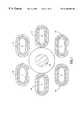
- FIG. 1illustrates a top view of a portion of a DRAM memory circuit from which the upper layers have been removed to reveal container capacitors 14 arranged around a bit line contact 16 .
- FIG. 1illustrates a top view of a portion of a DRAM memory circuit from which the upper layers have been removed to reveal container capacitors 14 arranged around a bit line contact 16 .
- FIG. 1illustrates a top view of a portion of a DRAM memory circuit from which the upper layers have been removed to reveal container capacitors 14 arranged around a bit line contact 16 .
- Six container capacitors 14are shown in FIG. 1, each of which has been labeled with separate reference designations A to F.
- the bit line contact 16is shared by DRAM cells corresponding to container capacitors A and B.
- the wall of each tubeconsists of two plates of conductive material such as doped polycrystalline silicon (referred to herein as polysilicon or poly) separated by a dielectric.
- the bottom end of the tubeis closed, with the outer wall in contact with either the drain of the access transistor or a plug which itself is in contact with the drain.
- the other end of the tubeis open (the tube is filled with an insulative material later in the fabrication process).
- the sidewall and closed end of the tubeform a container; hence the name “container capacitor.”
- the present inventionprovides a fabrication process and capacitor structure that achieves high storage capacitance without increasing the size of the capacitor or requiring complex fabrication steps.
- the present inventionprovides a three-dimensional capacitor cell which maintains high storage capacitance without increasing cell area.
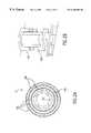
- the capacitor cell of the present inventionincludes a container capacitor having a concentrically formed internal fin as shown, for example, in FIG. 2 B.
- the fabrication processis advantageous in its simplicity, requiring only two additional deposition steps, a spacer etch and a wet etch.
- FIG. 1is a top view of a cross section of a known memory circuit showing a number of conventionally shaped container.capacitors surrounding a bit line contact.
- FIG. 2Ais top view of a partially cut away cross section of one embodiment of a memory circuit according to the present invention showing the finned container capacitor of FIG. 15 below.
- FIG. 2Bis a partial three dimensional view of one embodiment of a memory circuit according to the present invention showing the finned container capacitor of FIG. 12 below.
- FIG. 3is a diagrammatic cross-sectional view of a portion of a semiconductor wafer at an early processing step according to one embodiment of the present invention.
- FIG. 4is a diagrammatic cross-sectional view of a portion of a semiconductor wafer at a processing step subsequent to that shown in FIG. 3 .
- FIG. 5is a diagrammatic cross-sectional view of a portion of a semiconductor wafer at a processing step subsequent to that shown in FIG. 4 .
- FIG. 6is a diagrammatic cross-sectional view of a portion of a semiconductor wafer at a processing step subsequent to that shown in FIG. 5 .
- FIG. 7is a diagrammatic cross-sectional view of a portion of a semiconductor wafer at a processing step subsequent to that shown in FIG. 6 .
- FIG. 8is a diagrammatic cross-sectional view of a portion of a semiconductor wafer at a processing step subsequent to that shown in FIG. 7 .
- FIG. 9is a diagrammatic cross-sectional view of a portion of a semiconductor wafer at a processing step subsequent to that shown in FIG. 8 .
- FIG. 10is a diagrammatic cross-sectional view of a portion of a semiconductor wafer at a processing step subsequent to that shown in FIG. 9 .
- FIG. 11is a diagrammatic cross-sectional view of a portion of a semiconductor wafer at a processing step subsequent to that shown in FIG. 10 .
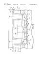
- FIG. 12is a diagrammatic cross-sectional view of a portion of a semiconductor wafer at a processing step subsequent to that shown in FIG. 11 .
- FIG. 13is a diagrammatic cross-sectional view of a portion of a semiconductor wafer at a processing step subsequent to that shown in FIG. 12 .
- FIG. 14is a diagrammatic cross-sectional view of a portion of a semiconductor wafer at a processing step subsequent to that shown in FIG. 13 .
- FIG. 15is a diagrammatic cross-sectional view of a portion of a semiconductor wafer at a processing step subsequent to that shown in FIG. 14 .
- FIG. 16is a diagrammatic cross-sectional view of a portion of a semiconductor wafer at a processing step subsequent to that shown in FIG. 15 .
- FIG. 17is a diagrammatic cross-sectional view of a portion of a semiconductor wafer at a processing step subsequent to that shown in FIG. 16 .
- FIG. 18is a diagrammatic cross-sectional view of a portion of a semiconductor wafer of another embodiment of the invention just prior to the processing step shown in FIG. 13 .
- FIG. 19is a schematic flow chart of a computer system.
- bit lineis formed over the capacitor in the following process.
- a buried bit-line processcould also be used.
- the plugs under the capacitors formed by the following processcould be eliminated.
- dry or wet etchingcould be used rather than chemical mechanical polishing. The invention is not intended to be limited by the particular process described below.
- a semiconductor wafer fragment at an early processing stepis indicated generally by reference numeral 100 .
- the semiconductor wafer 100is comprised of a bulk silicon substrate 112 with field isolation oxide regions 114 and active areas 116 , 118 , 120 formed therein.
- Word lines 122 , 124 , 126 , 128have been constructed on the wafer 100 in a conventional manner. Each word line consists of a lower gate oxide 130 , a lower poly layer 132 , a higher conductivity silicide layer 134 and an insulating silicon nitride cap 136 . Each word line has also been provided with insulating spacers 138 , which are also composed of silicon nitride.
- Two FETsare depicted in FIG. 3 .
- One FETis comprised of two active areas (source/drain) 116 , 118 and one word line (gate) 124 .
- the second FETis comprised of two active areas (source/drain) 118 , 120 and a second word line (gate) 126 .
- the active area 118 common to both FETsis the active area over which a bit line contact will be formed. As discussed above, one bit line contact is shared by two DRAM cells to conserve space.
- a thin layer 140 of nitride or TEOS(tetraethyl orthosilicate) is then provided atop the wafer 100 .
- a layer of insulating material 142is deposited.
- the insulating materialpreferably consists of borophosphosilicate glass (BPSG).
- BPSGborophosphosilicate glass
- CMPchemical-mechanical polishing
- plug openingshave been formed through the insulating layer 142 .
- the plug openings 144are formed through the insulating layer 142 by photomasking and dry chemical etching the BPSG relative to the thin nitride layer 140 .
- a layer 146 of conductive materialis deposited to provide conductive material within the plug openings 144 .
- the conductive plug layer 146is in contact with the active areas 116 , 118 , 120 .
- An example of the material used to form conductive plug layer 146is in situ arsenic or phosphorous doped poly. Referring now to FIG.
- the conductive plug layer 146is dry etched (or chemical-mechanical polished) to a point just below the upper surface of the BPSG layer 142 such that the remaining material of the conductive plug layer 146 forms electrically isolated plugs 146 over the active areas 116 , 118 , 120 .
- an additional layer 148 of BPSGis then deposited on the structure.
- Capacitor container openings 150 having sidewalls 151are then formed in the BPSG layer 148 by photomasking and dry chemical etching. The height of the plugs, as defined by the conductive plug layer 146 over the non-bit line active areas 116 , 120 is also reduced by this step.
- a conformal sacrificial layer 152 of, for example, doped polyis deposited to cover the container sidewalls, including the exposed portions of plugs 146 and insulating layers 142 and 148 .
- Layer 152is typically deposited to a thickness of 200 to 2000 Angstroms, more preferably about 500 to 1000 Angstroms.
- a thin spacer layer 153 of nitride or TEOSis then deposited over sacrificial layer 152 .
- layer 153is then spacer etched to form cylindrical spacers 154 concentric with the container sidewalls.
- Layer 153may be spacered using any anisotropic etch process, including reactive ion etching (REI) or other techniques known in the art, and may be deposited using any typical spacer material, so long as the sacrificial layer 152 may be etched selective to the material chosen for spacer 154 .
- REIreactive ion etching
- sacrificial layer 152is then removed, resulting in the structure shown in FIG. 12 and in FIG. 2 B.
- This removalis preferably performed by a wet etch process using tetramethyl ammonium hydroxide (TMAH).
- TMAHtetramethyl ammonium hydroxide
- TMAHhas a very slow SiO 2 etch rate relative to the rate it etches silicon (i.e., TEOS).
- Other etchantsmay also be used as long as they are capable of etching sacrificial layer 152 selective to the material of spacer 154 .
- the etch of layer 152is preferably timed to etch for a certain duration depending on the thickness of layer 152 , such that layer 152 is not completely removed from between container sidewall 151 and the outside surface of spacer 154 which would otherwise allow spacer 154 to float away.
- a typical duration for the TMAH wet etch for a 500 Angstrom thickness of sacrificial layer 152 of polyis in the range of about 2 to 5 min.
- the etch duration and thicknesses of layer 152 and spacer 154may be readily selected and optimized by those in the art given the teachings herein and the characteristics of the materials chosen for the etchant, sacrificial layer 152 and spacer 154 .
- the etchantmay also remove a portion of plugs 146 . Preferably, at least a portion of plugs 146 will remain in place in order to guard against the occurrence of junction damage.
- a capacitance layer 155is next deposited over the remaining sacrificial layer 152 and spacers 154 .
- the capacitance layer 155is also in electrical contact with the previously formed plugs 146 over the non-bit line active areas 116 , 120 .
- the capacitance layer 155may be formed of any conductive material, preferably HSG (hemispherical grained poly), silica, silicon, germanium or an alloy of silica or germanium, to increase capacitance. Most preferably, the capacitance layer 155 is formed of HSG. If HSG is used, capacitance layer 155 may be formed by first depositing a layer of in situ doped polysilicon followed by a deposition of undoped HSG. Subsequent heating inherent in wafer processing will effectively conductively dope the overlying HSG layer. Alternatively, the capacitance layer 155 may be provided by in situ arsenic doping of an entire HSG layer.
- the portion of the capacitance layer 155 above the top of the second BPSG layer 148is removed through a CMP or etching process, thereby electrically isolating the portions of the capacitance layer 155 remaining in the capacitor openings 150 .
- a dielectric film layer 156is formed over the surface of capacitance layer 155 .
- the preferred dielectric filmshave a high dielectric constant, including, for example, cell dielectrics such as Ta 2 O 5 , SrTiO 3 (“ST”), (Ba, Sr)TiO 3 (“BST”), Pb(Z,Ti)O 3 (“PZT”), SrBi 2 Ta 2 O 9 (“SBT”) and Ba(Zr,Ti)O 3 (“BZT”).
- the dielectric film layer 156will typically have a thickness of from about 10 to about 50 Angstroms.
- Layer 156may be deposited, for example, by a low-pressure CVD process using Ta(OC 2 H 5 ) 5 and O 2 at about 430° C., and may be subsequently annealed to minimize leakage current characteristics.
- a conductive layer 157is deposited to form the top electrode over the dielectric layer 156 , again at a thickness which less than completely fills the capacitor opening 150 .
- the only requirement for the selection of the conductive layer 157is that the material is conductive.
- Non-limiting examples of materials that may be used to form the conductive layer 157are RuO 2 , Ir, IrO 2 , Ta, Rh, RhO x , VO 3 , and alloys, such as Pt—Ru or Pt—Rh.
- the conductive layer 157may be deposited by CVD, LPCVD, PECVD, MOCVD, sputtering or other suitable deposition techniques.
- the conductive layer 157has a thickness of about 100 to about 1000 Angstroms, more preferably less than 500 Angstroms.
- the conductive layer 157also forms the interconnection lines between the second plates of the capacitors. The second plate of the capacitor is connected to the reference voltage.
- bit line insulating layer 158is provided over the conductive layer 157 and the second BPSG layer 148 .
- the bit line insulating layer 158may be comprised of BPSG, PSG, flowable glass, spun glass or other insulative material.
- bit line insulating layer 158is BPSG.
- a bit line contact opening 160is patterned through the bit line insulating layer 158 such that the conductive plug layer 146 is once again outwardly exposed.
- bit line contact opening 160a bit line contact is provided in the bit line contact opening 160 such that the bit line contact is in electrical contact with the outwardly exposed portion of the plug 146 .
- the outwardly exposed portion of the plug 146 over the active area 118 common to both FETsacts as a bit line contact.
- a further preferred embodiment of the fabrication process of the inventionbegins at FIG. 8 after conductive layer 146 is provided in plug openings 144 and etched back to form conductive plugs in contact with active areas 116 , 120 .
- a thin protective layer 161 of TEOS or other protective materialis deposited to protect the conductive plugs 146 during the subsequent wet etch processing.
- the protective TEOS layer 161is then removed from the bottom of the container opening to expose the surface of the plug 146 prior to deposition of the capacitance layer 155 .
- the thin TEOS layer 161may remain on the container sidewall 151 .
- the resulting structure, prior to deposition of the capacitance layer 155is then as shown in FIG. 18 .
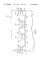
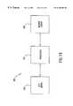
- FIG. 19illustrates a computer system 300 according to one embodiment of the present invention.
- the computer system 300comprises a CPU (central processing unit) 302 , a memory circuit 304 , and an I/O (input/output) device 306 .
- the memory circuit 304contains a DRAM memory circuit including the finned capacitors according to the present invention. Memory other than DRAM may be used. Also, the CPU itself may be an integrated processor which utilizes integrated capacitors according to the present invention.
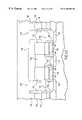
- FIG. 2Ashows a top view of a capacitor according to the invention from which the upper layers have been removed to reveal the finned container capacitor 15 .
- Capacitor 15has a concentric internal fin as a result of the form of spacer 154 , both sides of which are coated with a capacitance materia 155 which is in electrical contact with the plug 146 , as also shown in FIG. 14 .
- capacitance layer 155also covers the exposed portion of the container sidewall 151 .
- the capacitance layer 155has three discrete layers in cross-section, all within the area of the container cell.
- dielectric layer 156atop the capacitance layer 155 on both the inside and outside of the spacer fin 154 are dielectric film layers formed of dielectric layer 156 .
- dielectric layer 156is comprised of a high dielectric constant material such as Ta 2 O 5
- capacitance layer 155is comprised of HSG.
- the effective storage capacity of capacitor 15will be high due to the triple capacitance layer (HSG) 155 on the inside and outside of the capacitor fin, and the dual layered dielectric layer 156 , again on the inside and outside of the fin (spacer 154 ).
- HSGtriple capacitance layer
- the dual layered dielectric layer 156again on the inside and outside of the fin (spacer 154 ).
- the capacitance per areais increased due to the increased surface area of the capacitor and the fabrication of the capacitor as described above.
- the present inventiontherefore provides an increased effective capacitance and a high capacitance per cell without increasing the size of the cell or capacitor, enabling an increased efficiency for the cell without a corresponding increase in size or additional complex fabrication steps.
Landscapes
- Semiconductor Memories (AREA)
Abstract
Description
Claims (32)
Priority Applications (2)
| Application Number | Priority Date | Filing Date | Title |
|---|---|---|---|
| US09/136,892US6188100B1 (en) | 1998-08-19 | 1998-08-19 | Concentric container fin capacitor |
| US09/715,001US6312986B1 (en) | 1998-08-19 | 2000-11-20 | Concentric container fin capacitor and method |
Applications Claiming Priority (1)
| Application Number | Priority Date | Filing Date | Title |
|---|---|---|---|
| US09/136,892US6188100B1 (en) | 1998-08-19 | 1998-08-19 | Concentric container fin capacitor |
Related Child Applications (1)
| Application Number | Title | Priority Date | Filing Date |
|---|---|---|---|
| US09/715,001DivisionUS6312986B1 (en) | 1998-08-19 | 2000-11-20 | Concentric container fin capacitor and method |
Publications (1)
| Publication Number | Publication Date |
|---|---|
| US6188100B1true US6188100B1 (en) | 2001-02-13 |
Family
ID=22474864
Family Applications (2)
| Application Number | Title | Priority Date | Filing Date |
|---|---|---|---|
| US09/136,892Expired - LifetimeUS6188100B1 (en) | 1998-08-19 | 1998-08-19 | Concentric container fin capacitor |
| US09/715,001Expired - Fee RelatedUS6312986B1 (en) | 1998-08-19 | 2000-11-20 | Concentric container fin capacitor and method |
Family Applications After (1)
| Application Number | Title | Priority Date | Filing Date |
|---|---|---|---|
| US09/715,001Expired - Fee RelatedUS6312986B1 (en) | 1998-08-19 | 2000-11-20 | Concentric container fin capacitor and method |
Country Status (1)
| Country | Link |
|---|---|
| US (2) | US6188100B1 (en) |
Cited By (11)
| Publication number | Priority date | Publication date | Assignee | Title |
|---|---|---|---|---|
| US20030008469A1 (en)* | 1999-04-12 | 2003-01-09 | Samsung Electronics Co., Ltd. | DRAM cell capacitor and manufacturing method thereof |
| US20030052375A1 (en)* | 2001-09-20 | 2003-03-20 | Hiroki Koga | Semiconductor device and method of manufacturing the same |
| US6537874B2 (en)* | 2000-08-31 | 2003-03-25 | Fujitsu Limited | Method for fabricating semiconductor device having a capacitor |
| US6740531B2 (en)* | 2000-08-11 | 2004-05-25 | Samsung Electronics Co., Ltd. | Method of fabricating integrated circuit devices having dielectric regions protected with multi-layer insulation structures |
| US20060240634A1 (en)* | 2003-09-17 | 2006-10-26 | Tran Luan C | DRAM access transistor and method of formation |
| US20080032424A1 (en)* | 2006-08-03 | 2008-02-07 | Micron Technology, Inc. | ALD of Zr-substituted BaTiO3 films as gate dielectrics |
| US20090032954A1 (en)* | 2007-07-31 | 2009-02-05 | Sang-Ho Kim | Semiconductor device and method of fabricating the same |
| US20100144141A1 (en)* | 2008-12-09 | 2010-06-10 | Park Sang-Su | Semiconductor Device and Method of Forming the Same |
| US20140145303A1 (en)* | 2012-11-26 | 2014-05-29 | Samsung Electronics Co., Ltd. | Semiconductor device and method of fabricating the same |
| US10515801B2 (en) | 2007-06-04 | 2019-12-24 | Micron Technology, Inc. | Pitch multiplication using self-assembling materials |
| US20230157005A1 (en)* | 2021-11-16 | 2023-05-18 | Nanya Technology Corporation | Semiconductor device and manufacturing method thereof |
Families Citing this family (10)
| Publication number | Priority date | Publication date | Assignee | Title |
|---|---|---|---|---|
| KR100388682B1 (en)* | 2001-03-03 | 2003-06-25 | 삼성전자주식회사 | Storage electric terminal layer and method for forming thereof |
| US6673700B2 (en)* | 2001-06-30 | 2004-01-06 | Ovonyx, Inc. | Reduced area intersection between electrode and programming element |
| US6458652B1 (en) | 2001-08-20 | 2002-10-01 | Micron Technology, Inc. | Methods of forming capacitor electrodes |
| GB2386471B (en)* | 2001-12-11 | 2004-04-07 | Samsung Electronics Co Ltd | A method for fabricating a one-cylinder stack capacitor |
| US6962846B2 (en)* | 2003-11-13 | 2005-11-08 | Micron Technology, Inc. | Methods of forming a double-sided capacitor or a contact using a sacrificial structure |
| US7312120B2 (en) | 2004-09-01 | 2007-12-25 | Micron Technology, Inc. | Method for obtaining extreme selectivity of metal nitrides and metal oxides |
| US7329576B2 (en)* | 2004-09-02 | 2008-02-12 | Micron Technology, Inc. | Double-sided container capacitors using a sacrificial layer |
| US7859026B2 (en)* | 2006-03-16 | 2010-12-28 | Spansion Llc | Vertical semiconductor device |
| TWI366890B (en)* | 2008-12-31 | 2012-06-21 | Ind Tech Res Inst | Method of manufacturing through-silicon-via and through-silicon-via structure |
| JP2014120615A (en)* | 2012-12-17 | 2014-06-30 | Fujitsu Semiconductor Ltd | Capacity element, capacity array, and a/d converter |
Citations (12)
| Publication number | Priority date | Publication date | Assignee | Title |
|---|---|---|---|---|
| US5234858A (en) | 1990-11-16 | 1993-08-10 | Micron Technology, Inc. | Stacked surrounding wall capacitor |
| US5236855A (en) | 1990-11-06 | 1993-08-17 | Micron Technology, Inc. | Stacked V-cell capacitor using a disposable outer digit line spacer |
| US5262662A (en) | 1991-10-31 | 1993-11-16 | Micron Technology, Inc. | Storage node capacitor having tungsten and etched tin storage node capacitor plate |
| US5266513A (en) | 1990-10-24 | 1993-11-30 | Micron Technology, Inc. | Method of making stacked W-cell capacitor |
| US5323038A (en) | 1992-04-16 | 1994-06-21 | Micron Technology, Inc. | Array of finned memory cell capacitors on a semiconductor substrate |
| US5371701A (en) | 1990-10-10 | 1994-12-06 | Micron Technology, Inc. | Stacked delta cell capacitor |
| US5438011A (en) | 1995-03-03 | 1995-08-01 | Micron Technology, Inc. | Method of forming a capacitor using a photoresist contact sidewall having standing wave ripples |
| US5534458A (en)* | 1993-06-23 | 1996-07-09 | Mitsubishi Denki Kabushiki Kaisha | Method of manufacturing a semiconductor device with high dielectric capacitor having sidewall spacers |
| US5604147A (en) | 1995-05-12 | 1997-02-18 | Micron Technology, Inc. | Method of forming a cylindrical container stacked capacitor |
| US5652164A (en) | 1993-04-07 | 1997-07-29 | Micron Technology, Inc. | Semiconductor processing methods of forming stacked capacitors |
| US5729054A (en)* | 1994-08-01 | 1998-03-17 | Texas Instruments Incorporated | Conductive noble-metal-insulator-alloy barrier layer for high-dielectric-constant material electrodes |
| US5892702A (en)* | 1993-07-07 | 1999-04-06 | Mitsubishi Denki Kabushiki Kaisha | Semiconductor memory device and method of manufacturing the same |
Family Cites Families (7)
| Publication number | Priority date | Publication date | Assignee | Title |
|---|---|---|---|---|
| US6002149A (en)* | 1990-11-19 | 1999-12-14 | Micron Technology, Inc. | Capacitor structures for memory cells |
| US5137842A (en)* | 1991-05-10 | 1992-08-11 | Micron Technology, Inc. | Stacked H-cell capacitor and process to fabricate same |
| US5150276A (en)* | 1992-01-24 | 1992-09-22 | Micron Technology, Inc. | Method of fabricating a vertical parallel cell capacitor having a storage node capacitor plate comprising a center fin effecting electrical communication between itself and parallel annular rings |
| KR0126799B1 (en)* | 1993-12-31 | 1997-12-29 | 김광호 | Capacitor Manufacturing Method of Semiconductor Device |
| KR0154161B1 (en)* | 1994-06-30 | 1998-10-15 | 김주용 | Capacitor Manufacturing Method of Semiconductor Device |
| US5856220A (en)* | 1996-02-08 | 1999-01-05 | Taiwan Semiconductor Manufacturing Company, Ltd. | Method for fabricating a double wall tub shaped capacitor |
| US6146937A (en)* | 1997-08-29 | 2000-11-14 | United Microelectronics Corp. | Method of forming a DRAM device utilizing a sacrificial doped oxide layer |
- 1998
- 1998-08-19USUS09/136,892patent/US6188100B1/ennot_activeExpired - Lifetime
- 2000
- 2000-11-20USUS09/715,001patent/US6312986B1/ennot_activeExpired - Fee Related
Patent Citations (12)
| Publication number | Priority date | Publication date | Assignee | Title |
|---|---|---|---|---|
| US5371701A (en) | 1990-10-10 | 1994-12-06 | Micron Technology, Inc. | Stacked delta cell capacitor |
| US5266513A (en) | 1990-10-24 | 1993-11-30 | Micron Technology, Inc. | Method of making stacked W-cell capacitor |
| US5236855A (en) | 1990-11-06 | 1993-08-17 | Micron Technology, Inc. | Stacked V-cell capacitor using a disposable outer digit line spacer |
| US5234858A (en) | 1990-11-16 | 1993-08-10 | Micron Technology, Inc. | Stacked surrounding wall capacitor |
| US5262662A (en) | 1991-10-31 | 1993-11-16 | Micron Technology, Inc. | Storage node capacitor having tungsten and etched tin storage node capacitor plate |
| US5323038A (en) | 1992-04-16 | 1994-06-21 | Micron Technology, Inc. | Array of finned memory cell capacitors on a semiconductor substrate |
| US5652164A (en) | 1993-04-07 | 1997-07-29 | Micron Technology, Inc. | Semiconductor processing methods of forming stacked capacitors |
| US5534458A (en)* | 1993-06-23 | 1996-07-09 | Mitsubishi Denki Kabushiki Kaisha | Method of manufacturing a semiconductor device with high dielectric capacitor having sidewall spacers |
| US5892702A (en)* | 1993-07-07 | 1999-04-06 | Mitsubishi Denki Kabushiki Kaisha | Semiconductor memory device and method of manufacturing the same |
| US5729054A (en)* | 1994-08-01 | 1998-03-17 | Texas Instruments Incorporated | Conductive noble-metal-insulator-alloy barrier layer for high-dielectric-constant material electrodes |
| US5438011A (en) | 1995-03-03 | 1995-08-01 | Micron Technology, Inc. | Method of forming a capacitor using a photoresist contact sidewall having standing wave ripples |
| US5604147A (en) | 1995-05-12 | 1997-02-18 | Micron Technology, Inc. | Method of forming a cylindrical container stacked capacitor |
Cited By (28)
| Publication number | Priority date | Publication date | Assignee | Title |
|---|---|---|---|---|
| US20030008469A1 (en)* | 1999-04-12 | 2003-01-09 | Samsung Electronics Co., Ltd. | DRAM cell capacitor and manufacturing method thereof |
| US6670663B2 (en)* | 1999-04-12 | 2003-12-30 | Samsung Electronics Co., Ltd. | DRAM cell capacitor and manufacturing method thereof |
| US6740531B2 (en)* | 2000-08-11 | 2004-05-25 | Samsung Electronics Co., Ltd. | Method of fabricating integrated circuit devices having dielectric regions protected with multi-layer insulation structures |
| US20040183116A1 (en)* | 2000-08-11 | 2004-09-23 | Hag-Ju Cho | Integrated circuit devices having dielectric regions protected with multi-layer insulation structures and methods of fabricating same |
| US7023037B2 (en) | 2000-08-11 | 2006-04-04 | Samsung Electronics Co., Ltd. | Integrated circuit devices having dielectric regions protected with multi-layer insulation structures |
| US6537874B2 (en)* | 2000-08-31 | 2003-03-25 | Fujitsu Limited | Method for fabricating semiconductor device having a capacitor |
| US20030052375A1 (en)* | 2001-09-20 | 2003-03-20 | Hiroki Koga | Semiconductor device and method of manufacturing the same |
| US6914309B2 (en)* | 2001-09-20 | 2005-07-05 | Nec Corporation | Semiconductor device with double sidewall spacer and layered contact |
| US20050196944A1 (en)* | 2001-09-20 | 2005-09-08 | Hiroki Koga | Semiconductor device and method of manufacturing the same |
| US20100200925A1 (en)* | 2001-09-20 | 2010-08-12 | Elpida Memory, Inc. | Semiconductor device and method of manufacturing the same |
| US7709366B2 (en) | 2001-09-20 | 2010-05-04 | Elpida Memory, Inc. | Semiconductor device and method of manufacturing the same |
| US7547604B2 (en)* | 2003-09-17 | 2009-06-16 | Micron Technology, Inc. | Method of forming a recessed gate structure on a substrate having insulating columns and removing said insulating columns after forming a conductive region of the gate structure |
| US7518184B2 (en) | 2003-09-17 | 2009-04-14 | Micron Technology, Inc. | DRAM access transistor |
| US20070176232A1 (en)* | 2003-09-17 | 2007-08-02 | Tran Luan C | DRAM access transistor and method of formation |
| US20060240634A1 (en)* | 2003-09-17 | 2006-10-26 | Tran Luan C | DRAM access transistor and method of formation |
| US8772050B2 (en)* | 2006-08-03 | 2014-07-08 | Micron Technology, Inc. | Zr-substituted BaTiO3 films |
| US20080032424A1 (en)* | 2006-08-03 | 2008-02-07 | Micron Technology, Inc. | ALD of Zr-substituted BaTiO3 films as gate dielectrics |
| US7985995B2 (en)* | 2006-08-03 | 2011-07-26 | Micron Technology, Inc. | Zr-substituted BaTiO3 films |
| US8323988B2 (en) | 2006-08-03 | 2012-12-04 | Micron Technology, Inc. | Zr-substituted BaTiO3 films |
| US20130122609A1 (en)* | 2006-08-03 | 2013-05-16 | Micron Technology, Inc. | Zr-SUBSTITUTED BaTiO3 FILMS |
| US10515801B2 (en) | 2007-06-04 | 2019-12-24 | Micron Technology, Inc. | Pitch multiplication using self-assembling materials |
| US20090032954A1 (en)* | 2007-07-31 | 2009-02-05 | Sang-Ho Kim | Semiconductor device and method of fabricating the same |
| US7999294B2 (en)* | 2007-07-31 | 2011-08-16 | Samsung Electronics Co., Ltd. | Semiconductor device which may prevent electrical failures of contacts |
| US20100144141A1 (en)* | 2008-12-09 | 2010-06-10 | Park Sang-Su | Semiconductor Device and Method of Forming the Same |
| US8119536B2 (en)* | 2008-12-09 | 2012-02-21 | Samsung Electronics Co., Ltd. | Semiconductor device and method of forming the same |
| US20140145303A1 (en)* | 2012-11-26 | 2014-05-29 | Samsung Electronics Co., Ltd. | Semiconductor device and method of fabricating the same |
| US9142610B2 (en)* | 2012-11-26 | 2015-09-22 | Samsung Electronics Co., Ltd. | Semiconductor device including supporters on a lower electrode thereof and method of fabricating the same |
| US20230157005A1 (en)* | 2021-11-16 | 2023-05-18 | Nanya Technology Corporation | Semiconductor device and manufacturing method thereof |
Also Published As
| Publication number | Publication date |
|---|---|
| US6312986B1 (en) | 2001-11-06 |
Similar Documents
| Publication | Publication Date | Title |
|---|---|---|
| US6188100B1 (en) | Concentric container fin capacitor | |
| US6737696B1 (en) | DRAM capacitor formulation using a double-sided electrode | |
| US5907782A (en) | Method of forming a multiple fin-pillar capacitor for a high density dram cell | |
| US7268039B2 (en) | Method of forming a contact using a sacrificial structure | |
| US6362042B1 (en) | DRAM having a cup-shaped storage node electrode recessed within an insulating layer | |
| US5994181A (en) | Method for forming a DRAM cell electrode | |
| US6114201A (en) | Method of manufacturing a multiple fin-shaped capacitor for high density DRAMs | |
| US5851876A (en) | Method of manufacturing dynamic random access memory | |
| US5994197A (en) | Method for manufacturing dynamic random access memory capable of increasing the storage capacity of the capacitor | |
| US20020000596A1 (en) | Method for improved processing and etchback of a container capacitor | |
| US6064085A (en) | DRAM cell with a multiple fin-shaped structure capacitor | |
| US5998260A (en) | Method for manufacturing DRAM capacitor | |
| US7112508B2 (en) | Method for forming conductive material in opening and structure regarding same | |
| US5981334A (en) | Method of fabricating DRAM capacitor | |
| US6054394A (en) | Method of fabricating a dynamic random access memory capacitor | |
| US6111285A (en) | Boride electrodes and barriers for cell dielectrics | |
| US6555454B2 (en) | Semiconductor memory device incorporating therein ruthenium electrode and method for the manufacture thereof | |
| US5874335A (en) | Method of fabricating DRAM capacitors | |
| US6080621A (en) | Method of manufacturing dynamic random access memory | |
| US6011286A (en) | Double stair-like capacitor structure for a DRAM cell | |
| US6207498B1 (en) | Method of fabricating a coronary-type capacitor in an integrated circuit | |
| KR100356826B1 (en) | Semiconductor device and fabricating method thereof | |
| US6329264B1 (en) | Method for forming a ragged polysilcon crown-shaped capacitor for a memory cell | |
| US6583006B2 (en) | Method to reduce floating grain defects in dual-sided container capacitor fabrication | |
| US6100135A (en) | Method of forming a crown-fin shaped capacitor for a high density DRAM cell |
Legal Events
| Date | Code | Title | Description |
|---|---|---|---|
| AS | Assignment | Owner name:MICRON TECHNOLOGY, INC., IDAHO Free format text:ASSIGNMENT OF ASSIGNORS INTEREST;ASSIGNOR:HERMES, MICHAEL;REEL/FRAME:009398/0149 Effective date:19980814 | |
| STCF | Information on status: patent grant | Free format text:PATENTED CASE | |
| CC | Certificate of correction | ||
| FPAY | Fee payment | Year of fee payment:4 | |
| FEPP | Fee payment procedure | Free format text:PAYOR NUMBER ASSIGNED (ORIGINAL EVENT CODE: ASPN); ENTITY STATUS OF PATENT OWNER: LARGE ENTITY Free format text:PAYER NUMBER DE-ASSIGNED (ORIGINAL EVENT CODE: RMPN); ENTITY STATUS OF PATENT OWNER: LARGE ENTITY | |
| FPAY | Fee payment | Year of fee payment:8 | |
| FPAY | Fee payment | Year of fee payment:12 | |
| AS | Assignment | Owner name:U.S. BANK NATIONAL ASSOCIATION, AS COLLATERAL AGENT, CALIFORNIA Free format text:SECURITY INTEREST;ASSIGNOR:MICRON TECHNOLOGY, INC.;REEL/FRAME:038669/0001 Effective date:20160426 Owner name:U.S. BANK NATIONAL ASSOCIATION, AS COLLATERAL AGEN Free format text:SECURITY INTEREST;ASSIGNOR:MICRON TECHNOLOGY, INC.;REEL/FRAME:038669/0001 Effective date:20160426 | |
| AS | Assignment | Owner name:MORGAN STANLEY SENIOR FUNDING, INC., AS COLLATERAL AGENT, MARYLAND Free format text:PATENT SECURITY AGREEMENT;ASSIGNOR:MICRON TECHNOLOGY, INC.;REEL/FRAME:038954/0001 Effective date:20160426 Owner name:MORGAN STANLEY SENIOR FUNDING, INC., AS COLLATERAL Free format text:PATENT SECURITY AGREEMENT;ASSIGNOR:MICRON TECHNOLOGY, INC.;REEL/FRAME:038954/0001 Effective date:20160426 | |
| AS | Assignment | Owner name:U.S. BANK NATIONAL ASSOCIATION, AS COLLATERAL AGENT, CALIFORNIA Free format text:CORRECTIVE ASSIGNMENT TO CORRECT THE REPLACE ERRONEOUSLY FILED PATENT #7358718 WITH THE CORRECT PATENT #7358178 PREVIOUSLY RECORDED ON REEL 038669 FRAME 0001. ASSIGNOR(S) HEREBY CONFIRMS THE SECURITY INTEREST;ASSIGNOR:MICRON TECHNOLOGY, INC.;REEL/FRAME:043079/0001 Effective date:20160426 Owner name:U.S. BANK NATIONAL ASSOCIATION, AS COLLATERAL AGEN Free format text:CORRECTIVE ASSIGNMENT TO CORRECT THE REPLACE ERRONEOUSLY FILED PATENT #7358718 WITH THE CORRECT PATENT #7358178 PREVIOUSLY RECORDED ON REEL 038669 FRAME 0001. ASSIGNOR(S) HEREBY CONFIRMS THE SECURITY INTEREST;ASSIGNOR:MICRON TECHNOLOGY, INC.;REEL/FRAME:043079/0001 Effective date:20160426 | |
| AS | Assignment | Owner name:JPMORGAN CHASE BANK, N.A., AS COLLATERAL AGENT, ILLINOIS Free format text:SECURITY INTEREST;ASSIGNORS:MICRON TECHNOLOGY, INC.;MICRON SEMICONDUCTOR PRODUCTS, INC.;REEL/FRAME:047540/0001 Effective date:20180703 Owner name:JPMORGAN CHASE BANK, N.A., AS COLLATERAL AGENT, IL Free format text:SECURITY INTEREST;ASSIGNORS:MICRON TECHNOLOGY, INC.;MICRON SEMICONDUCTOR PRODUCTS, INC.;REEL/FRAME:047540/0001 Effective date:20180703 | |
| AS | Assignment | Owner name:MICRON TECHNOLOGY, INC., IDAHO Free format text:RELEASE BY SECURED PARTY;ASSIGNOR:U.S. BANK NATIONAL ASSOCIATION, AS COLLATERAL AGENT;REEL/FRAME:047243/0001 Effective date:20180629 | |
| AS | Assignment | Owner name:MICRON TECHNOLOGY, INC., IDAHO Free format text:RELEASE BY SECURED PARTY;ASSIGNOR:MORGAN STANLEY SENIOR FUNDING, INC., AS COLLATERAL AGENT;REEL/FRAME:050937/0001 Effective date:20190731 | |
| AS | Assignment | Owner name:MICRON TECHNOLOGY, INC., IDAHO Free format text:RELEASE BY SECURED PARTY;ASSIGNOR:JPMORGAN CHASE BANK, N.A., AS COLLATERAL AGENT;REEL/FRAME:051028/0001 Effective date:20190731 Owner name:MICRON SEMICONDUCTOR PRODUCTS, INC., IDAHO Free format text:RELEASE BY SECURED PARTY;ASSIGNOR:JPMORGAN CHASE BANK, N.A., AS COLLATERAL AGENT;REEL/FRAME:051028/0001 Effective date:20190731 |