US6188028B1 - Multilayer structure with interlocking protrusions - Google Patents
Multilayer structure with interlocking protrusionsDownload PDFInfo
- Publication number
- US6188028B1 US6188028B1US09/094,089US9408998AUS6188028B1US 6188028 B1US6188028 B1US 6188028B1US 9408998 AUS9408998 AUS 9408998AUS 6188028 B1US6188028 B1US 6188028B1
- Authority
- US
- United States
- Prior art keywords
- contact
- opening
- conductive layer
- post
- circuit panel
- Prior art date
- Legal status (The legal status is an assumption and is not a legal conclusion. Google has not performed a legal analysis and makes no representation as to the accuracy of the status listed.)
- Expired - Lifetime
Links
Images


Classifications
- H—ELECTRICITY
- H05—ELECTRIC TECHNIQUES NOT OTHERWISE PROVIDED FOR
- H05K—PRINTED CIRCUITS; CASINGS OR CONSTRUCTIONAL DETAILS OF ELECTRIC APPARATUS; MANUFACTURE OF ASSEMBLAGES OF ELECTRICAL COMPONENTS
- H05K3/00—Apparatus or processes for manufacturing printed circuits
- H05K3/46—Manufacturing multilayer circuits
- H05K3/4611—Manufacturing multilayer circuits by laminating two or more circuit boards
- H05K3/4614—Manufacturing multilayer circuits by laminating two or more circuit boards the electrical connections between the circuit boards being made during lamination
- H05K3/4617—Manufacturing multilayer circuits by laminating two or more circuit boards the electrical connections between the circuit boards being made during lamination characterized by laminating only or mainly similar single-sided circuit boards
- H—ELECTRICITY
- H01—ELECTRIC ELEMENTS
- H01R—ELECTRICALLY-CONDUCTIVE CONNECTIONS; STRUCTURAL ASSOCIATIONS OF A PLURALITY OF MUTUALLY-INSULATED ELECTRICAL CONNECTING ELEMENTS; COUPLING DEVICES; CURRENT COLLECTORS
- H01R12/00—Structural associations of a plurality of mutually-insulated electrical connecting elements, specially adapted for printed circuits, e.g. printed circuit boards [PCB], flat or ribbon cables, or like generally planar structures, e.g. terminal strips, terminal blocks; Coupling devices specially adapted for printed circuits, flat or ribbon cables, or like generally planar structures; Terminals specially adapted for contact with, or insertion into, printed circuits, flat or ribbon cables, or like generally planar structures
- H01R12/50—Fixed connections
- H01R12/51—Fixed connections for rigid printed circuits or like structures
- H01R12/52—Fixed connections for rigid printed circuits or like structures connecting to other rigid printed circuits or like structures
- H01R12/523—Fixed connections for rigid printed circuits or like structures connecting to other rigid printed circuits or like structures by an interconnection through aligned holes in the boards or multilayer board
- H—ELECTRICITY
- H05—ELECTRIC TECHNIQUES NOT OTHERWISE PROVIDED FOR
- H05K—PRINTED CIRCUITS; CASINGS OR CONSTRUCTIONAL DETAILS OF ELECTRIC APPARATUS; MANUFACTURE OF ASSEMBLAGES OF ELECTRICAL COMPONENTS
- H05K3/00—Apparatus or processes for manufacturing printed circuits
- H05K3/30—Assembling printed circuits with electric components, e.g. with resistor
- H05K3/32—Assembling printed circuits with electric components, e.g. with resistor electrically connecting electric components or wires to printed circuits
- H05K3/325—Assembling printed circuits with electric components, e.g. with resistor electrically connecting electric components or wires to printed circuits by abutting or pinching, i.e. without alloying process; mechanical auxiliary parts therefor
- H—ELECTRICITY
- H05—ELECTRIC TECHNIQUES NOT OTHERWISE PROVIDED FOR
- H05K—PRINTED CIRCUITS; CASINGS OR CONSTRUCTIONAL DETAILS OF ELECTRIC APPARATUS; MANUFACTURE OF ASSEMBLAGES OF ELECTRICAL COMPONENTS
- H05K2201/00—Indexing scheme relating to printed circuits covered by H05K1/00
- H05K2201/09—Shape and layout
- H05K2201/09209—Shape and layout details of conductors
- H05K2201/095—Conductive through-holes or vias
- H05K2201/09509—Blind vias, i.e. vias having one side closed
- H—ELECTRICITY
- H05—ELECTRIC TECHNIQUES NOT OTHERWISE PROVIDED FOR
- H05K—PRINTED CIRCUITS; CASINGS OR CONSTRUCTIONAL DETAILS OF ELECTRIC APPARATUS; MANUFACTURE OF ASSEMBLAGES OF ELECTRICAL COMPONENTS
- H05K2201/00—Indexing scheme relating to printed circuits covered by H05K1/00
- H05K2201/09—Shape and layout
- H05K2201/09818—Shape or layout details not covered by a single group of H05K2201/09009 - H05K2201/09809
- H05K2201/09845—Stepped hole, via, edge, bump or conductor
- H—ELECTRICITY
- H05—ELECTRIC TECHNIQUES NOT OTHERWISE PROVIDED FOR
- H05K—PRINTED CIRCUITS; CASINGS OR CONSTRUCTIONAL DETAILS OF ELECTRIC APPARATUS; MANUFACTURE OF ASSEMBLAGES OF ELECTRICAL COMPONENTS
- H05K2203/00—Indexing scheme relating to apparatus or processes for manufacturing printed circuits covered by H05K3/00
- H05K2203/11—Treatments characterised by their effect, e.g. heating, cooling, roughening
- H05K2203/1184—Underetching, e.g. etching of substrate under conductors or etching of conductor under dielectrics; Means for allowing or controlling underetching
- H—ELECTRICITY
- H05—ELECTRIC TECHNIQUES NOT OTHERWISE PROVIDED FOR
- H05K—PRINTED CIRCUITS; CASINGS OR CONSTRUCTIONAL DETAILS OF ELECTRIC APPARATUS; MANUFACTURE OF ASSEMBLAGES OF ELECTRICAL COMPONENTS
- H05K3/00—Apparatus or processes for manufacturing printed circuits
- H05K3/46—Manufacturing multilayer circuits
- H05K3/4644—Manufacturing multilayer circuits by building the multilayer layer by layer, i.e. build-up multilayer circuits
- H05K3/4647—Manufacturing multilayer circuits by building the multilayer layer by layer, i.e. build-up multilayer circuits by applying an insulating layer around previously made via studs
- Y—GENERAL TAGGING OF NEW TECHNOLOGICAL DEVELOPMENTS; GENERAL TAGGING OF CROSS-SECTIONAL TECHNOLOGIES SPANNING OVER SEVERAL SECTIONS OF THE IPC; TECHNICAL SUBJECTS COVERED BY FORMER USPC CROSS-REFERENCE ART COLLECTIONS [XRACs] AND DIGESTS
- Y10—TECHNICAL SUBJECTS COVERED BY FORMER USPC
- Y10T—TECHNICAL SUBJECTS COVERED BY FORMER US CLASSIFICATION
- Y10T29/00—Metal working
- Y10T29/49—Method of mechanical manufacture
- Y10T29/49002—Electrical device making
- Y10T29/49117—Conductor or circuit manufacturing
- Y10T29/49124—On flat or curved insulated base, e.g., printed circuit, etc.
- Y10T29/49126—Assembling bases
Definitions
- the present inventionrelates to the field of electrical circuitry, for example, the electrical and mechanical interconnection of layers in a multilayer structure, and more particularly, relates to layered circuit structures such as multilayer circuit panels, to components and methods utilized in fabrication of such structures and to methods of making the same.
- Circuit panelsordinarily include a generally flat sheet of dielectric material with electrical conductors disposed on a major, flat surface of the sheet or on both major surfaces.
- the conductorsare commonly formed from metallic materials such as copper and serve to interconnect the electrical components mounted to the board. Where the conductors are disposed on both major surfaces of the panel, the panel may have via conductors extending through the dielectric layer so as to interconnect the conductors on opposite surfaces.
- Multilayer circuit panel assemblieshave been made heretofore which incorporate plural, stacked circuit panels with additional layers of dielectric materials separating the conductors on mutually facing surfaces of adjacent panels in the stack. These multilayer assemblies ordinarily incorporate interconnections extending between the conductors on the various circuit panels in the stack as necessary to provide the required electrical interconnections.
- circuit panel structuresinclude so-called “discrete”, components and integrated circuits which include numerous transistors on a single chip.
- Chips of this naturecan be mounted to elements commonly referred to as “chip carriers” which are specialized circuit panel structures.
- a chip carriermay be incorporated in a package which is mounted to a larger circuit panel and interconnected with the remaining elements of the circuit.
- the chipcan be mounted directly to the same circuit panel which carries other components of the system. This arrangement is ordinarily referred to as a “hybrid circuit”.
- Relatively large circuit panelsare commonly made of polymeric materials, typically with reinforcement such as glass, whereas very small circuit panels such as those used as semiconductor chip carriers may be formed from ceramics, silicon or the like.
- Multilayer panelsare commonly made by providing individual, dual sided circuit panels with appropriate conductors thereon. The panels are then laminated one atop the other with one or more layers of uncured or partially cured dielectric material, commonly referred to as “prepregs” disposed between each pair of adjacent panels. Such a stack ordinarily is cured under heat and pressure to form a unitary mass. After curing, holes are drilled through the stack at locations where electrical connections between different boards are desired.
- the resulting holesare then coated or filled with electrically conductive materials, typically by plating the interiors of the holes to form what is called a plated through hole.
- electrically conductive materialstypically by plating the interiors of the holes to form what is called a plated through hole. It is difficult to drill holes with a high ratio of depth to diameter.
- the holes used in assemblies fabricated according to these prior methodsmust be relatively large and hence consume substantial amounts of space in the assembly. These holes ordinarily extend from the top or bottom of the stack. Even where interconnections are not required in the top or bottom layers, space must be provided for holes to pass through these layers so as to provide needed interconnections in the middle layers. Accordingly, substantial amounts of the available surface area on the panels must be allocated to the holes and to accommodate tolerance zones around the holes.
- the electrical interconnections formed by depositing conductive materials in such drilled holestend to be weak.
- the drilling method and the general nature of the laminates used thereinis described, for example in Doherty, Jr., U.S. Pat.
- Such a sheetmay be sandwiched between a pair of circuit panels and the circuit panels may be clamped or otherwise held together so as to provide mechanical engagement between conductive elements on the adjacent faces of the circuit panels and the conductive elements of the composite sheet.
- the conductive elements, the composite sheet or bothis resilient or malleable so as to provide for close engagement between the conductive elements of the composite sheet and the conductors on the circuit panels.
- Patraw, U.S. Pat. Nos. 4,716,049; 4,902,606; and 4,924,353,describe microelectronic connection schemes using deformable contacts protruding upwardly from a substrate.
- Each contacthas a dome-like tip and a plurality of legs extending downwardly from the tip to the substrate.
- These contactsare formed by selective deposition of aluminum on pedestals of a fugitive material such as potassium chloride or a photoresist using a shaped mask. The pedestals are removed after deposition.
- Feigenbaum, et al., U.S. Pat. No. 5,354,205discloses forming connections between layers in a multilayer circuit panel by providing a plated via in one of the layers of the circuit panel, and providing a tapered protrusion having a conical or pyramidal shape aligned with the via on an adjacent layer of the circuit panel.
- the circuit panelis not configured to enable connection for multiple stacking of one circuit panel to another.
- the disclosed configurationrelies upon the use of tapered protrusions in the form of male members which wedge into the circumferential opening of the plated vias. This connection which has small surface area contact is not always reliable thereby forming a potential failure point.
- the present inventionbroadly relates to circuit panels having a plurality of connectors which may be interconnected over their major opposing surfaces by conductive circuit traces.
- the circuit panelsare interconnected into a multilayer stack of circuit panels using the connectors, and optionally, an intermediate adhesive or compliant layer.
- the connectorsinclude two contacts provided on either side of the circuit panel which is in the nature of a sheet-like layer or body of dielectric material.
- a thru hole in the dielectric layerextends between the two contacts.
- a holeis provided in one of the contacts which is aligned with the hole in the dielectric layer, the other contact being a solid contact.
- the hole in the dielectric layer, together with the hole in the contactare plated to form a plated blind via connection at its lower end to the solid contact.
- the plating of the inner surfaces of the holesextends continuously from the blind end where it connects to the solid contact, to the open end where it forms an upper layer of the contact having a hole.
- the post-like bumpmay have a bulbous, arrow-shaped, or other configured end portion at its distal end for mating in an adjoining via, or may be uniformly cylindrical or of other uniform cross section.
- Adjacent circuit panels and their delineated tracesmay be interconnected by aligning a contact on one layer with a contact on an adjacent layer, and then applying a force to insert the post-like bump into the plated via through the hole in the contact.
- Multiple circuit panel layersmay be interconnected using stacked connectors according to the present invention.
- the post-like bumphas an enlarged portion at its distal end
- the plated viamay be provided with an enlarged portion below the surface of the contact pad, providing a “snap fit” with the post-like bump.
- a post-like bump having a uniform cross sectionmay be used. In such a configuration, the post-like bump has a diameter slightly larger than the plated via, to provide an interference fit whereby a wiping action occurs during insertion.
- a dielectric sheetlike element or bodyis first covered on both major surfaces with metallic layers such as a copper layer.
- the metallic layersmay be laminated onto the dielectric layer or may be plated. Openings are then etched through one of the two metallic layers using an acid or other etching solution. Each etched hole extends through the metallic layer to the surface of the dielectric layer. Vias aligned with the openings in the metal layer are then formed in the dielectric layer using a laser, chemical or plasma etching process.
- the nature of the etching processtypically forms vias having a larger diameter at their upper surfaces and a smaller diameter at their blind ends.
- the hole in the dielectric layermay be larger than the hole in the metal layer to provide a “snap fit” as described above.
- a hole substantially corresponding in size to the hole in the metallic layer having a constant cross-sectional area, such as is formed using laser drilling,may be etched or otherwise formed in the dielectric layer.
- the vias in the dielectric layer and the metallic layerare next plated with copper, gold or other conductive metal or alloy.
- the top surface of the upper metal layeris plated together with the entire internal geometry of the via.
- the blind end of the viais formed by the upper surface of the bottom metallic layer.
- the plated via at this stage of the processelectrically interconnects the upper and lower metallic layers.
- the metallic layers, together with the plated surface on the upper metallic layer,are etched to form metallic contact pads surrounding the vias on either side of the dielectric layer.
- interconnecting circuit tracesmay also be formed on the dielectric layer for interconnecting various contacts.
- a post-like bumpis formed on the bottom side of the bottom metal layer. As discussed above, the post may or may not have a bulbous distal end for snap fitting in the via.
- the post-like bumpmay be formed, for example, by plating a hole in a sacrificial mask layer.
- the connector of the present inventionprovides a low inductance connection between layers in a multilayer structure when connecting circuit panels such as when used as an interposer.
- the circular viasby their nature, create relatively low levels of inductance when conducting current.
- the blind viamay contain conductive material before insertion of the male connector member, i.e., post-like bump.
- the conductive materialmay be contained within an enlarged portion of the via formed in the dielectric layer. The conductive material mechanically and electrically bonds the via to the post-like bump.
- the post-like bumpmay be longer than the vertical clearance provided in the blind via.
- the post-like bumpis partially crushed during assembly into the via as the bump bottoms on the lower contact. The crushing provides additional wiping action between the two elements, and the crushed post may act as a retainer, preventing the post-like bump from sliding out of the via.
- a layer of dielectric adhesive or compliant materialmay be provided on one or both surfaces of adjoining dielectric layers to seal the regions surrounding the contacts, and to support and mechanically connect the dielectric layers in regions between contacts.
- the adhesivemay be provided as a sheet having holes corresponding to the contacts. The sheet is aligned with the contacts on the dielectric layer, and assembled onto the dielectric layer before adjoining dielectric layers are assembled.
- the adhesivemay be a flowable adhesive printed or stenciled onto the dielectric layer before assembly.
- a connectorfor making electrical connection to an element having a body defining first and second surfaces opposing each other and an opening extending through the body between the first and second surfaces, the connector comprising a first contact on the first surface proximate the opening, a second contact on the second surface overlying the opening, a conductive layer lining the interior of the opening within the body and in contact with the first and second contacts, and a post extending away from the second surface in contact with the second contact.
- a circuit panelfor making electrical connection to contacts on an adjacent circuit panel, the circuit panel comprising a body defining first and second surfaces opposing each other, an opening extending through the body between the first and second surfaces, a first contact on the first surface surrounding the opening thereat, a second contact on the second surface overlying the opening thereat, a conductive layer lining the interior of the opening within the body in contact with the first and second contacts, the conductive layer defining an opening within the body having a blind end adjacent the second surface in contact with the second contact and an open end extending through the first contact, the conductive layer extending over a portion of the surface of the first contact, and a post extending from the second contact in alignment with the opening formed by the conductive layer.
- a method of making a connector for an element having a body defining first and second surfaces opposing each othercomprising the steps of forming a first contact on the first surface and a second contact on the second surface in alignment with the first contact, forming an opening through the first contact and the body terminating at the second contact, depositing a conductive layer lining the interior of the opening within the body and in contact with the first and second contacts and forming a post extending away from the second surface in contact with the second contact.
- a method of making a circuit panel for making electrical connection to contacts on an adjacent circuit panelincluding a body defining first and second surfaces opposing each other, the method comprising the steps of forming an opening extending through the body between the first and second surfaces, forming a first contact on the first surface surrounding the opening thereat and a second contact on the second surface overlying the opening thereat, depositing a conductive layer lining the interior of the opening within the body in contact with the first and second contacts and over a portion of the surface of the first contact, the conductive layer defining an opening within the body having a blind end adjacent the second surface in contact with the second contact and an open end extending through the first contact, and forming a post extending from the second contact in alignment with the opening formed by the conductive layer.
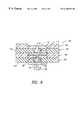
- FIG. 1is a schematic perspective view showing an assembled multilayer structure of interconnected circuit panels constructed and assembled according to the present invention
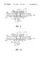
- FIG. 2is a cross-sectional view of a connector in accordance with one embodiment of the present invention for interconnecting a plurality of circuit panels in a multilayer stack;
- FIGS. 3-7are cross-sectional views showing various stages in the fabrication of a connector in a circuit panel in accordance with one embodiment of the present invention.
- FIG. 8is a cross-sectional view showing a multilayer stack of circuit panels interconnected using connectors as shown in FIG. 2;
- FIG. 9is a cross-sectional view of a connector in accordance with another embodiment of the present invention for interconnecting a plurality of circuit panels in a multilayer stack.
- FIG. 10is a cross-sectional view of a connector in accordance with another embodiment of the present invention for interconnecting a plurality of circuit panels in a multilayer stack.
- FIG. 1a multilayer structure generally designated by reference numeral 100 .
- the structure 100is composed of a plurality of stacked separate circuit panels 102 , three such circuit panels being shown by way of example only, which are interconnected in accordance with the present invention.
- Each circuit panel 102incorporates a body 104 of dielectric material having oppositely directed major upper and lower surfaces 106 , 108 .
- the area of the major surfaces 106 , 108are substantially greater than the area of the edge surfaces 110 connecting the major surfaces.
- the bodyis substantially flat and sheet-like such that the major surfaces 106 , 108 are substantially parallel to one another.
- Each circuit panel 102is provided with a plurality of thru connectors generally designated by reference numeral 112 .
- the connectorsmay be provided within the circuit panels 102 in a regular or irregular array, such as a rectilinear grid, for example, rows and columns. It is also contemplated that the connectors 112 may be arranged randomly within the circuit panels 102 . As will be described hereinafter, each of the connectors 112 extend through the body 104 so as to have contact pads provided on the major surfaces 106 , 108 as shown in FIG. 2 .
- the connectors 112 on surfaces 106 , 108may be interconnected in a predetermined pattern by providing interconnecting circuit traces 114 .
- the particular interconnection patternwill depend upon the purpose and layout of the electrical components (not shown) which will ultimately be mounted and/or connected to the multilayer structure 100 .
- the electrical componentsmay be provided in a variety of forms, for example, discrete components, semiconductive chips and the like.
- the circuit traces 114thus form electrical conductive paths between the connectors 112 on the surfaces 106 , 108 of the circuit panels 102 .
- the circuit panel 102is formed from a body 104 of dielectric material, for example polyimide material. Electrical contacts 116 , 118 are provided on opposing surfaces 106 , 108 spaced apart by the body 104 . The contacts 116 , 118 are aligned with an opening or hole 120 formed within the body 104 which extends between the major surfaces 106 , 108 . Contact 116 is provided with an opening or hole 122 which is aligned in communication with opening 120 and opposing a portion of contact 118 on surface 108 . Opening 122 is preferably of other than circular shape.
- the opening 122may be in the shape of a three or four leaf clover as shown in FIG. 1 .
- This shapeprovides inwardly directed prongs which provide for a better interference fit and welding of the post when inserted therein as to be described.
- a clover-like shape, or other than circular shapeallows for misregistration tolerances of the post pitch.
- Contact 116is formed from a contact pad 124 through which opening 122 extends.
- the contact pad 124is formed directly on the surface 106 of the body 104 surrounding opening 122 .
- Contact 116further includes an outer layer 126 which further defines a conductive layer 128 lining opening 122 in contact pad 124 and opening 120 in the body 104 of the circuit panel 102 .
- Conductive layer 128has a base portion 130 in engagement with the exposed portion of contact 118 within opening 120 so as to form a blind end to the opening adjacent surface 108 .
- the conductive layer 128conforms to the shape of opening 120 , thereby providing a generally corresponding shaped interior opening 132 which is in communication with opening 122 .
- opening 122has an effective diameter generally smaller than the effective diameter of the interior opening 132 .
- effective diameterit is generally meant, in particular as to non-spherical shapes, that the overall size of the opening 122 will be smaller than the overall size of the interior opening 132 .
- the conductive layer 128forms a lip 134 surrounding opening 122 where it communicates with the interior opening 132 .
- Contact 118is formed from a solid contact pad 136 directly on surface 108 having a portion engaged by the base portion 130 of conductive layer 128 which forms the blind end of opening 120 .
- a post-like element 138is provided extending outwardly from the surface of contact pad 136 .
- the post 138is formed in the nature of a solid post-like bump having a distal end portion 140 .
- the post 138may have any cross-sectional shape, for example, circular, oval, rectangular and the like.
- the distal end portion 140may have any desired cross sectional shape. As shown, the distal end portion 140 has a trapezoidal shape which generally corresponds to the shape of the interior opening 132 formed by the conductive layer 128 in the embodiment thus described.
- the effective diameter of the distal end portion 140is slightly greater than the diameter of opening 122 which extends through contact 116 and into the interior opening 132 .
- the effective size of interior opening 132may also be slightly smaller than the effective size of the distal end portion 140 to attain a friction fit therebetween.
- a dielectric body 104in the nature of a sheet-like element, is first covered on both major surfaces 106 , 108 with metallic layers 142 , 144 such as a copper, copper-nickel, berylium-copper layer and the like.
- the metallic layers 142 , 144may be laminated onto the surfaces 106 , 108 of the body 104 or may be plated using conventional electroplating processes.
- an opening 146is etched through metallic layer 142 using a photoresist mask which is applied over the surface of the metallic layer 142 where the openings 146 are to be formed.
- the maskmay be applied as a discrete, preformed element, or else may be formed by photographic techniques.
- the maskmay be formed from any suitable material, including a polymer material such as photoresist, a sheet of molybdenum, or may include a layer of molybdenum on a polymeric substrate.
- the exposed metallic layer 142is etched using a suitable etching such as an acid or other etching solution.
- the etched opening 146extends through the metallic layer 142 to the surface 106 of the dielectric body 104 .
- an opening 120 in the nature of a viais formed in the dielectric body 104 by ablation, for example, using radiant energy directed through opening 146 , or chemical plasma etching processing. Opening 120 will therefore have the same shape as opening 146 , for example, non-circular.
- the radiant energy applied to provide this ablationtypically includes a C 0 2 , excimer, yag or Krf laser operating under conditions which will substantially ablate the dielectric body 104 , but which will not substantially affect the material of the metallic layer 142 .
- opening 120having a larger diameter at its upper end 148 adjacent metallic layer 142 and a smaller diameter at its blind end 150 adjacent metallic layer 144 .
- This resulting configuration of the opening 120is believed to be due to the longer exposure time to the etch solution at the upper end 148 of the opening 120 than at the blind end 150 .
- opening 146 in the metallic layer 142smaller than the resulting opening 120 in the dielectric body 104 , this provides for a snap fit as previously described.
- a conductive layer 152such as gold, copper or other conductive metals and alloys is deposited over the surface of metallic layer 142 and into the opening 120 .
- the entire top surface 154 of the metallic layer 142is plated together with the entire internal surfaces of the opening 120 formed within the dielectric body 104 , which may also include a tin flashing to enhance bonding with the post 138 .
- the blind end 150is formed by surface 156 of the metallic layer 144 in the region overlying opening 120 .
- the conductive layer 152electrically interconnects the upper and lower metallic layers 142 , 144 .
- Contacts 116are completed on the major surface 106 using a suitable photoresist mask or the like so as to define the geometry and location of the contact pads 124 .
- the interconnecting circuit traces 114may also be formed from the metallic layer 142 and conductive layer 152 so as to interconnect the various connectors 112 throughout the circuit panel 102 in the desired pattern.
- the exposed portions of the metallic layer 142 and conductive layer 152may be removed using ablation, such as by laser, or chemical or plasma etching processes.
- the previous stepwill define the geometry and location of each of the connectors 112 and interconnecting circuit traces 114 simultaneously on the surface 106 of the body 104 .
- a suitable photoresist mask 158 and the likemay be used to delineate the contacts 118 and interconnecting circuit traces 114 from metallic layer 144 which has been provided on the opposing surface 108 of the body 104 .
- the contact pads 136 of each contact 118will be aligned overlying the opening 120 so as to provide electrical interconnection with conductive layer 128 which interconnects with contacts 116 on the upper surface 106 of body 104 .
- the circuit traces 114 on the upper and lower surfaces 106 , 108are therefore interconnected in a predetermined pattern via the connectors 112 which are formed through the body 104 by virtue of the conductive layer 128 electrically connecting contacts 116 , 118 .
- Post 138is formed on the resulting contact pad 136 which was formed from the metallic layer 144 .
- Post 138can be deposited separately onto the exposed surface of the contact pad 136 by additive electroplating or chemical vapor deposition using a photographically patterned resist with open areas corresponding to the configuration of the post.
- the post 138can be formed by first depositing a sacrificial metal layer onto the exposed surface of the contact pad 136 using conventional semiconductor processing, and subsequently etching the sacrificial metal layer to form the post 138 using a photographically patterned resist.
- the post 138can also be formed by mechanically removing an upper portion of the sacrificial metal layer such as by grinding, ablation and the like.
- the post 138may have a coating of gold to prevent oxidation and to enhance welding, such as cold welding, to the conductive layer 128 of an adjacent connector 112 .
- the postmay be coated with an anti-tarnish polymer layer which is removed by the bonding process.
- the postmay have a tin flashing and the conductive layer formed of gold to enhance bonding of the post in the connector. It should therefore be apparent that the post can be configured to any desirable shape and size as may be desired.
- the completed connector 112has a post 138 which includes a distal end portion 140 of trapezoidal shape.
- the post 138may have a diameter of about 1-2 mils., its length L′′ being in the range of about 1-4 mils., and preferably about 2 mils.
- the length of the post 138will, in part, depend on whether it is desirable to have the post crushed during the insertion process. In this regard, the length of the post 138 will ultimately depend on the thickness of the circuit panel 102 , the contact pad 124 , outer layer 126 , and optionally, adhesive layer 160 . By way of example, the combined thickness of contact pad 124 and outer layer 126 is in the range of about 5-25 microns. From the foregoing, it should be understood that the aspect ratio of the post 138 can be other than 1:1, i.e., the length being greater than the diameter, particularly when it is desired that the post crush during insertion into the connector 112 .
- a plurality of circuit panels 102may be interconnected to one another to form a multilayer structure 100 having interconnected traces 114 .
- the individual circuit panels 102are interconnected by aligning the connectors 112 on one circuit panel 102 with a corresponding connector on an adjacent circuit panel. A sufficient force is applied between the two circuit panels 102 so as to insert the distal end portion 140 of post 138 into the connector 112 through opening 122 whereby the distal end portion is captured within the interior opening 132 defined by the conductive layer 128 .
- FIG. 128In accordance with one embodiment as shown in FIG.
- the post 138has an enlarged distal end portion which is captured within the interior opening 132 in the manner of a snap fit by virtue of opening 122 within contact pad 124 being effectively smaller in size.
- a plurality of circuit panels 102may be interconnected using stacked connectors 112 in accordance with the present invention. As shown, the configuration and dimensioning of the connectors 112 will generally result in the contact pad 136 of one circuit panel 102 abutting against the contact pad 124 of an adjacent circuit panel.
- the connectors 112 of the present inventionprovide a low inductance connection between a plurality of circuit panels 102 in a multilayer structure 100 .
- the construction of the connectors 112for example, by providing a snap or interference fit with the post 138 , creates relatively low levels of inductance when conducting current therethrough.
- the connector 112may be provided with an electrically conductive material before assembly of the circuit panels 102 into a multilayer structure 100 by insertion of a post 138 into the connector.
- the conductive materialis generally provided within the interior opening 132 formed in the connector 112 by the conductive layer 128 .
- the conductive materialmechanically and electrically bonds the post 138 to the interior of the conductor 112 .
- the conductive materialmay be a solder paste such as a polymer/metal bonding material which includes a dispersion of a metal such as silver or gold particles in a thermoplastic polymer such as Ultem material or thermosetting polymer such as an epoxy.
- a layer 160 of dielectric adhesive or similar compliant material in the range of about 25-50 microns thickmay be provided on one or both surfaces 106 , 108 of adjoining circuit panels 102 to seal the regions surrounding contacts 116 , 118 , and to support and mechanically connect the circuit panels in regions between the contacts.
- the adhesive or compliant materialmay be provided as a sheet having holes corresponding to the size and locations of the contacts. The sheet is initially aligned with the contacts 116 , 118 on one of the surfaces 106 , 108 , and assembled onto the circuit panel 102 before adjoining the adjacent circuit panel to form the multilayer structure 100 . It is not required that the adhesive layer 160 have preformed openings. In this regard, the posts 138 will penetrate the adhesive layer 160 overlying the openings 122 during their insertion into the connectors 112 .
- the adhesivemay be a flowable adhesive printed or stenciled onto one or both of the surfaces 106 , 108 of the circuit panels 102 before assembly. It is contemplated that the openings 122 , particularly when enlarged such as in clover shape, will allow excess adhesive to flow into the interior opening 132 during the assembly process. This will eliminate excess adhesive around the connectors 112 to provide a flatter or more planar multilayer structure 100 . In addition, any adhesive within the interior opening 132 will enhance the mechanical bonding of the post within the connector 112 , which is facilitated by its cold welding therein.
- the adhesive or compliant layer 160may be formed from dielectric materials such as polyimide, polyetherimide and the like.
- the post 138is formed as a uniform elongated cylindrical member.
- the openings 122 , 132are defined by the conductive layer 128 .
- the opening 120 in the dielectric body 104 which during fabrication defines the shape of interior opening 132may therefore have a cross-sectional area as noted hereinabove which can be formed using laser drilling, or other such ablation techniques.
- the post 138may have a diameter slightly larger than that formed in an adjacent connector 112 to provide an interference fit whereby a wiping action occurs during insertion which will facilitate removal of any oxide layer, as well as providing intimate surface-to-surface contact for positive electrical continuity therebetween.
- the wiping actionmay further induce friction welding or “cold” welding between those two components, forming a permanent mechanical bond.
- the openings 122 , 132may be of other than circular shape, such as three and four leaf clover shape, oval or the like. Here again, this allows for misregistration of the posts 138 .
- Post 138may be longer in length L′′ than the vertical clearance provided in the connector 112 designated as length L′.
- the post 138is partially crushed during assembly when inserted into the connector 112 as its distal end portion 140 bottoms out against the conductive layer 128 opposing contact pad 136 .
- the crushingprovides additional wiping action between the aforementioned elements, and the crushed post 138 will therefore function as a retainer element within the interior opening 132 of the connector 112 , preventing the post from sliding out from the connector.
- the distal end portion 140is formed having a spherical bulbous shape as opposed to the cylindrical shape shown in FIG. 9 or the trapezoidal shape as shown in FIG. 2 .
- the bulbous shapewill provided for a snap fit as previously described with respect to the circuit panel 102 shown in FIG. 2 .
- the interior opening 132 within the connector 112also has a generally spherical bulbous shape. It should therefore be appreciated that the shape of the post 138 , and particularly the distal end portion 140 may have a variety of forms and configurations, as well as the interior opening 132 .
Landscapes
- Engineering & Computer Science (AREA)
- Manufacturing & Machinery (AREA)
- Microelectronics & Electronic Packaging (AREA)
- Metallurgy (AREA)
- Coupling Device And Connection With Printed Circuit (AREA)
Abstract
Description
Claims (81)
Priority Applications (1)
| Application Number | Priority Date | Filing Date | Title |
|---|---|---|---|
| US09/094,089US6188028B1 (en) | 1997-06-09 | 1998-06-09 | Multilayer structure with interlocking protrusions |
Applications Claiming Priority (2)
| Application Number | Priority Date | Filing Date | Title |
|---|---|---|---|
| US4902197P | 1997-06-09 | 1997-06-09 | |
| US09/094,089US6188028B1 (en) | 1997-06-09 | 1998-06-09 | Multilayer structure with interlocking protrusions |
Publications (1)
| Publication Number | Publication Date |
|---|---|
| US6188028B1true US6188028B1 (en) | 2001-02-13 |
Family
ID=26726797
Family Applications (1)
| Application Number | Title | Priority Date | Filing Date |
|---|---|---|---|
| US09/094,089Expired - LifetimeUS6188028B1 (en) | 1997-06-09 | 1998-06-09 | Multilayer structure with interlocking protrusions |
Country Status (1)
| Country | Link |
|---|---|
| US (1) | US6188028B1 (en) |
Cited By (42)
| Publication number | Priority date | Publication date | Assignee | Title |
|---|---|---|---|---|
| US6326559B1 (en)* | 1998-06-30 | 2001-12-04 | Matsushita Electric Works, Ltd. | Multilayer printed wiring board and method for manufacturing same |
| US6412168B1 (en)* | 2000-09-06 | 2002-07-02 | Visteon Global Tech, Inc. | Method of making an electrical circuit board |
| US6532654B2 (en)* | 2001-01-12 | 2003-03-18 | International Business Machines Corporation | Method of forming an electrical connector |
| US6647619B2 (en)* | 2001-10-22 | 2003-11-18 | Agilent Technologies, Inc. | Positioning arrangement and method |
| US6668448B2 (en)* | 1999-05-12 | 2003-12-30 | Microconnex Corp. | Method of aligning features in a multi-layer electrical connective device |
| US6717060B2 (en)* | 2000-05-15 | 2004-04-06 | Harting Elektro-Optische Bauteile Gmbh & Co. Kg | Circuit board consisting of at least two individual circuit board layers made of plastic |
| US20040069638A1 (en)* | 2002-09-30 | 2004-04-15 | The Regents Of The University Of California | Electrophoretic/electrochemical devices with nanometer-scale metallic components |
| US20040182604A1 (en)* | 2003-03-20 | 2004-09-23 | David Alcoe | Pinned electronic package with strengthened conductive pad |
| US6804881B1 (en)* | 2000-05-12 | 2004-10-19 | Shipley Company, L.L.C. | Multilayer circuit board manufacturing process |
| US20040229489A1 (en)* | 2003-03-09 | 2004-11-18 | Xiaocheng Lu | Circuit-toy assembly kit |
| US20060033518A1 (en)* | 2004-08-13 | 2006-02-16 | Lameres Brock J | Probe retention kit, and system and method for probing a pattern of points on a printed circuit board |
| US20060099833A1 (en)* | 2002-09-10 | 2006-05-11 | Saint-Gobain Glass France | Connecting device for a multilayer flat element equipped with electrical functional elements and flat element |
| US20060220259A1 (en)* | 2005-01-25 | 2006-10-05 | Ke-Hung Chen | Multi-chip structure and method of assembling chips |
| US20060249299A1 (en)* | 2004-07-13 | 2006-11-09 | Kummer Randy D | Electrical cable having a surface with reduced coefficient of friction |
| AU2002311385B2 (en)* | 2001-12-26 | 2007-04-05 | Sumitomo Wiring Systems, Ltd. | Temporary holding structure for connector holder |
| US20070232090A1 (en)* | 2006-03-31 | 2007-10-04 | Colgan Evan G | Space transforming land grid array interposers |
| US20080020227A1 (en)* | 2004-04-26 | 2008-01-24 | Formfactor, Inc. | Method To Build Robust Mechanical Structures On Substrate Surfaces |
| WO2008050448A1 (en)* | 2006-10-27 | 2008-05-02 | Asahi Denka Kenkyusho Co., Ltd. | Electrical connection structure |
| US20080180927A1 (en)* | 2007-01-26 | 2008-07-31 | Paul Coteus | Compliant Penetrating Packaging Interconnect |
| US20080185736A1 (en)* | 1999-02-08 | 2008-08-07 | Megica Corporation | Multiple selectable function integrated circuit module |
| KR100885121B1 (en) | 2007-08-29 | 2009-02-20 | 가부시키가이샤 아사히 덴카 겐큐쇼 | Electrical connection structure |
| WO2009025637A1 (en)* | 2007-08-20 | 2009-02-26 | California Institute Of Technology | Multilayered cellular metallic glass structures and methods of preparing the same |
| US20090053476A1 (en)* | 2007-08-20 | 2009-02-26 | Conner Robert D | Multilayered cellular metallic glass structures and methods of preparing the same |
| US20090057919A1 (en)* | 2000-05-19 | 2009-03-05 | Megica Corporation | Multiple chips bonded to packaging structure with low noise and multiple selectable functions |
| US20090057900A1 (en)* | 2005-05-03 | 2009-03-05 | Megica Corporation | Stacked Chip Package With Redistribution Lines |
| US20090183911A1 (en)* | 2008-01-21 | 2009-07-23 | Shinko Electric Industries Co., Ltd. | Wiring board and method of manufacturing the same |
| US20100212148A1 (en)* | 2007-06-01 | 2010-08-26 | Fumitomo Kawahara | Methods For Manufacturing and Reclaiming Electrode For Plasma Processing Apparatus |
| US7883939B2 (en) | 2008-11-11 | 2011-02-08 | Semiconductor Energy Laboratory Co., Ltd. | Method for manufacturing semiconductor device |
| CN101310416B (en)* | 2006-01-26 | 2011-02-09 | 松下电工株式会社 | Board-to-board connector |
| US8322906B2 (en) | 2011-08-08 | 2012-12-04 | XtraLight Manufacturing Partnership Ltd | Versatile lighting units |
| US8431208B2 (en) | 2007-08-20 | 2013-04-30 | California Institute Of Technology | Multilayered cellular metallic glass structures |
| US20130214390A1 (en)* | 2010-11-26 | 2013-08-22 | Industrial Technology Research Institute | Tsv substrate structure and the stacked assembly thereof |
| USRE45463E1 (en)* | 2003-11-12 | 2015-04-14 | Tessera, Inc. | Stacked microelectronic assemblies with central contacts |
| US9337613B1 (en)* | 2013-03-12 | 2016-05-10 | Western Digital Technologies, Inc. | Chip on submount carrier fixture |
| US20170064827A1 (en)* | 2014-02-21 | 2017-03-02 | Lg Innotek Co., Ltd. | Connector, circuit board module and circuit board module array including same |
| US9644829B2 (en) | 2013-04-25 | 2017-05-09 | Xtralight Manufacturing, Ltd. | Systems and methods for providing a field repairable light fixture with a housing that dissipates heat |
| US9942982B2 (en) | 1997-08-04 | 2018-04-10 | Continental Circuits, Llc | Electrical device with teeth joining layers and method for making the same |
| EP3402315A1 (en)* | 2017-05-11 | 2018-11-14 | FESTO AG & Co. KG | Connector and connector system |
| US20200194918A1 (en)* | 2017-03-06 | 2020-06-18 | Rosenberger Hochfrequenztechnik Gmbh & Co. Kg | Electrical contact element |
| EP2428486B1 (en)* | 2004-11-04 | 2021-04-14 | Microchips Biotech, Inc. | Compression and cold weld sealing methods and devices |
| CN115513686A (en)* | 2021-06-23 | 2022-12-23 | 鹏鼎控股(深圳)股份有限公司 | Board-to-board connection structure and manufacturing method thereof |
| US12408275B2 (en)* | 2021-07-16 | 2025-09-02 | Linxens Holding | Method for manufacturing multicoloured printed circuits for smart card modules |
Citations (34)
| Publication number | Priority date | Publication date | Assignee | Title |
|---|---|---|---|---|
| US3316618A (en) | 1963-12-09 | 1967-05-02 | Rca Corp | Method of making connection to stacked printed circuit boards |
| US3509270A (en) | 1968-04-08 | 1970-04-28 | Ney Co J M | Interconnection for printed circuits and method of making same |
| US3541222A (en) | 1969-01-13 | 1970-11-17 | Bunker Ramo | Connector screen for interconnecting adjacent surfaces of laminar circuits and method of making |
| US3616532A (en) | 1970-02-02 | 1971-11-02 | Sperry Rand Corp | Multilayer printed circuit electrical interconnection device |
| US3663931A (en)* | 1970-11-25 | 1972-05-16 | Collins Radio Co | Pin and socket contact electrical interconnect system |
| US3739469A (en) | 1971-12-27 | 1973-06-19 | Ibm | Multilayer printed circuit board and method of manufacture |
| US3795037A (en) | 1970-05-05 | 1974-03-05 | Int Computers Ltd | Electrical connector devices |
| US3862790A (en) | 1971-07-22 | 1975-01-28 | Plessey Handel Investment Ag | Electrical interconnectors and connector assemblies |
| US4249302A (en) | 1978-12-28 | 1981-02-10 | Ncr Corporation | Multilayer printed circuit board |
| US4548451A (en) | 1984-04-27 | 1985-10-22 | International Business Machines Corporation | Pinless connector interposer and method for making the same |
| US4655519A (en) | 1985-10-16 | 1987-04-07 | Amp Incorporated | Electrical connector for interconnecting arrays of conductive areas |
| US4707657A (en)* | 1984-06-13 | 1987-11-17 | Boegh Petersen Allan | Connector assembly for a circuit board testing machine, a circuit board testing machine, and a method of testing a circuit board by means of a circuit board testing machine |
| US4716049A (en) | 1985-12-20 | 1987-12-29 | Hughes Aircraft Company | Compressive pedestal for microminiature connections |
| US4729809A (en) | 1985-03-14 | 1988-03-08 | Amp Incorporated | Anisotropically conductive adhesive composition |
| US4788766A (en) | 1987-05-20 | 1988-12-06 | Loral Corporation | Method of fabricating a multilayer circuit board assembly |
| US4793814A (en) | 1986-07-21 | 1988-12-27 | Rogers Corporation | Electrical circuit board interconnect |
| US4902606A (en) | 1985-12-20 | 1990-02-20 | Hughes Aircraft Company | Compressive pedestal for microminiature connections |
| US4924353A (en) | 1985-12-20 | 1990-05-08 | Hughes Aircraft Company | Connector system for coupling to an integrated circuit chip |
| US4954878A (en) | 1989-06-29 | 1990-09-04 | Digital Equipment Corp. | Method of packaging and powering integrated circuit chips and the chip assembly formed thereby |
| US5129142A (en) | 1990-10-30 | 1992-07-14 | International Business Machines Corporation | Encapsulated circuitized power core alignment and lamination |
| US5167512A (en) | 1991-07-05 | 1992-12-01 | Walkup William B | Multi-chip module connector element and system |
| US5224265A (en) | 1991-10-29 | 1993-07-06 | International Business Machines Corporation | Fabrication of discrete thin film wiring structures |
| US5229647A (en)* | 1991-03-27 | 1993-07-20 | Micron Technology, Inc. | High density data storage using stacked wafers |
| US5228861A (en) | 1992-06-12 | 1993-07-20 | Amp Incorporated | High density electrical connector system |
| US5232548A (en) | 1991-10-29 | 1993-08-03 | International Business Machines Corporation | Discrete fabrication of multi-layer thin film, wiring structures |
| US5282312A (en) | 1991-12-31 | 1994-02-01 | Tessera, Inc. | Multi-layer circuit construction methods with customization features |
| US5354205A (en) | 1991-08-26 | 1994-10-11 | Hughes Aircraft Company | Electrical connections with shaped contacts |
| US5367764A (en) | 1991-12-31 | 1994-11-29 | Tessera, Inc. | Method of making a multi-layer circuit assembly |
| US5442143A (en)* | 1993-04-16 | 1995-08-15 | Dyconex Patente Ag | Core for electrical connecting substrates and electrical connecting substrates with core, as well as process for the production thereof |
| US5613033A (en)* | 1995-01-18 | 1997-03-18 | Dell Usa, Lp | Laminated module for stacking integrated circuits |
| US5758413A (en)* | 1995-09-25 | 1998-06-02 | International Business Machines Corporation | Method of manufacturing a multiple layer circuit board die carrier with fine dimension stacked vias |
| US5879787A (en)* | 1996-11-08 | 1999-03-09 | W. L. Gore & Associates, Inc. | Method and apparatus for improving wireability in chip modules |
| US5936848A (en)* | 1995-12-20 | 1999-08-10 | Intel Corporation | Electronics package that has a substrate with an array of hollow vias and solder balls that are eccentrically located on the vias |
| US5951305A (en) | 1998-07-09 | 1999-09-14 | Tessera, Inc. | Lidless socket and method of making same |
- 1998
- 1998-06-09USUS09/094,089patent/US6188028B1/ennot_activeExpired - Lifetime
Patent Citations (34)
| Publication number | Priority date | Publication date | Assignee | Title |
|---|---|---|---|---|
| US3316618A (en) | 1963-12-09 | 1967-05-02 | Rca Corp | Method of making connection to stacked printed circuit boards |
| US3509270A (en) | 1968-04-08 | 1970-04-28 | Ney Co J M | Interconnection for printed circuits and method of making same |
| US3541222A (en) | 1969-01-13 | 1970-11-17 | Bunker Ramo | Connector screen for interconnecting adjacent surfaces of laminar circuits and method of making |
| US3616532A (en) | 1970-02-02 | 1971-11-02 | Sperry Rand Corp | Multilayer printed circuit electrical interconnection device |
| US3795037A (en) | 1970-05-05 | 1974-03-05 | Int Computers Ltd | Electrical connector devices |
| US3663931A (en)* | 1970-11-25 | 1972-05-16 | Collins Radio Co | Pin and socket contact electrical interconnect system |
| US3862790A (en) | 1971-07-22 | 1975-01-28 | Plessey Handel Investment Ag | Electrical interconnectors and connector assemblies |
| US3739469A (en) | 1971-12-27 | 1973-06-19 | Ibm | Multilayer printed circuit board and method of manufacture |
| US4249302A (en) | 1978-12-28 | 1981-02-10 | Ncr Corporation | Multilayer printed circuit board |
| US4548451A (en) | 1984-04-27 | 1985-10-22 | International Business Machines Corporation | Pinless connector interposer and method for making the same |
| US4707657A (en)* | 1984-06-13 | 1987-11-17 | Boegh Petersen Allan | Connector assembly for a circuit board testing machine, a circuit board testing machine, and a method of testing a circuit board by means of a circuit board testing machine |
| US4729809A (en) | 1985-03-14 | 1988-03-08 | Amp Incorporated | Anisotropically conductive adhesive composition |
| US4655519A (en) | 1985-10-16 | 1987-04-07 | Amp Incorporated | Electrical connector for interconnecting arrays of conductive areas |
| US4902606A (en) | 1985-12-20 | 1990-02-20 | Hughes Aircraft Company | Compressive pedestal for microminiature connections |
| US4716049A (en) | 1985-12-20 | 1987-12-29 | Hughes Aircraft Company | Compressive pedestal for microminiature connections |
| US4924353A (en) | 1985-12-20 | 1990-05-08 | Hughes Aircraft Company | Connector system for coupling to an integrated circuit chip |
| US4793814A (en) | 1986-07-21 | 1988-12-27 | Rogers Corporation | Electrical circuit board interconnect |
| US4788766A (en) | 1987-05-20 | 1988-12-06 | Loral Corporation | Method of fabricating a multilayer circuit board assembly |
| US4954878A (en) | 1989-06-29 | 1990-09-04 | Digital Equipment Corp. | Method of packaging and powering integrated circuit chips and the chip assembly formed thereby |
| US5129142A (en) | 1990-10-30 | 1992-07-14 | International Business Machines Corporation | Encapsulated circuitized power core alignment and lamination |
| US5229647A (en)* | 1991-03-27 | 1993-07-20 | Micron Technology, Inc. | High density data storage using stacked wafers |
| US5167512A (en) | 1991-07-05 | 1992-12-01 | Walkup William B | Multi-chip module connector element and system |
| US5354205A (en) | 1991-08-26 | 1994-10-11 | Hughes Aircraft Company | Electrical connections with shaped contacts |
| US5232548A (en) | 1991-10-29 | 1993-08-03 | International Business Machines Corporation | Discrete fabrication of multi-layer thin film, wiring structures |
| US5224265A (en) | 1991-10-29 | 1993-07-06 | International Business Machines Corporation | Fabrication of discrete thin film wiring structures |
| US5282312A (en) | 1991-12-31 | 1994-02-01 | Tessera, Inc. | Multi-layer circuit construction methods with customization features |
| US5367764A (en) | 1991-12-31 | 1994-11-29 | Tessera, Inc. | Method of making a multi-layer circuit assembly |
| US5228861A (en) | 1992-06-12 | 1993-07-20 | Amp Incorporated | High density electrical connector system |
| US5442143A (en)* | 1993-04-16 | 1995-08-15 | Dyconex Patente Ag | Core for electrical connecting substrates and electrical connecting substrates with core, as well as process for the production thereof |
| US5613033A (en)* | 1995-01-18 | 1997-03-18 | Dell Usa, Lp | Laminated module for stacking integrated circuits |
| US5758413A (en)* | 1995-09-25 | 1998-06-02 | International Business Machines Corporation | Method of manufacturing a multiple layer circuit board die carrier with fine dimension stacked vias |
| US5936848A (en)* | 1995-12-20 | 1999-08-10 | Intel Corporation | Electronics package that has a substrate with an array of hollow vias and solder balls that are eccentrically located on the vias |
| US5879787A (en)* | 1996-11-08 | 1999-03-09 | W. L. Gore & Associates, Inc. | Method and apparatus for improving wireability in chip modules |
| US5951305A (en) | 1998-07-09 | 1999-09-14 | Tessera, Inc. | Lidless socket and method of making same |
Cited By (68)
| Publication number | Priority date | Publication date | Assignee | Title |
|---|---|---|---|---|
| US9942982B2 (en) | 1997-08-04 | 2018-04-10 | Continental Circuits, Llc | Electrical device with teeth joining layers and method for making the same |
| US6326559B1 (en)* | 1998-06-30 | 2001-12-04 | Matsushita Electric Works, Ltd. | Multilayer printed wiring board and method for manufacturing same |
| US20080185736A1 (en)* | 1999-02-08 | 2008-08-07 | Megica Corporation | Multiple selectable function integrated circuit module |
| US8013448B2 (en) | 1999-02-08 | 2011-09-06 | Megica Corporation | Multiple selectable function integrated circuit module |
| US8471389B2 (en) | 1999-02-08 | 2013-06-25 | Megica Corporation | Multiple selectable function integrated circuit module |
| US6668448B2 (en)* | 1999-05-12 | 2003-12-30 | Microconnex Corp. | Method of aligning features in a multi-layer electrical connective device |
| US6675473B2 (en)* | 1999-05-12 | 2004-01-13 | Microconnex Corp. | Method of positioning a conductive element in a laminated electrical device |
| US6804881B1 (en)* | 2000-05-12 | 2004-10-19 | Shipley Company, L.L.C. | Multilayer circuit board manufacturing process |
| US6717060B2 (en)* | 2000-05-15 | 2004-04-06 | Harting Elektro-Optische Bauteile Gmbh & Co. Kg | Circuit board consisting of at least two individual circuit board layers made of plastic |
| US20090057919A1 (en)* | 2000-05-19 | 2009-03-05 | Megica Corporation | Multiple chips bonded to packaging structure with low noise and multiple selectable functions |
| US8148806B2 (en) | 2000-05-19 | 2012-04-03 | Megica Corporation | Multiple chips bonded to packaging structure with low noise and multiple selectable functions |
| US6412168B1 (en)* | 2000-09-06 | 2002-07-02 | Visteon Global Tech, Inc. | Method of making an electrical circuit board |
| US6532654B2 (en)* | 2001-01-12 | 2003-03-18 | International Business Machines Corporation | Method of forming an electrical connector |
| US6647619B2 (en)* | 2001-10-22 | 2003-11-18 | Agilent Technologies, Inc. | Positioning arrangement and method |
| AU2002311385B2 (en)* | 2001-12-26 | 2007-04-05 | Sumitomo Wiring Systems, Ltd. | Temporary holding structure for connector holder |
| US20060099833A1 (en)* | 2002-09-10 | 2006-05-11 | Saint-Gobain Glass France | Connecting device for a multilayer flat element equipped with electrical functional elements and flat element |
| US7156666B2 (en)* | 2002-09-10 | 2007-01-02 | Saint-Gobain Glass France | Connecting device for a multilayer flat element equipped with electrical functional elements and flat element |
| US20040069638A1 (en)* | 2002-09-30 | 2004-04-15 | The Regents Of The University Of California | Electrophoretic/electrochemical devices with nanometer-scale metallic components |
| US20040229489A1 (en)* | 2003-03-09 | 2004-11-18 | Xiaocheng Lu | Circuit-toy assembly kit |
| US7087846B2 (en)* | 2003-03-20 | 2006-08-08 | Endicott Interconnect Technologies, Inc. | Pinned electronic package with strengthened conductive pad |
| US20040182604A1 (en)* | 2003-03-20 | 2004-09-23 | David Alcoe | Pinned electronic package with strengthened conductive pad |
| USRE45463E1 (en)* | 2003-11-12 | 2015-04-14 | Tessera, Inc. | Stacked microelectronic assemblies with central contacts |
| US20100224303A1 (en)* | 2004-04-26 | 2010-09-09 | Formfactor, Inc. | Method to build robust mechanical structures on substrate surfaces |
| US20080020227A1 (en)* | 2004-04-26 | 2008-01-24 | Formfactor, Inc. | Method To Build Robust Mechanical Structures On Substrate Surfaces |
| US7732713B2 (en)* | 2004-04-26 | 2010-06-08 | Formfactor, Inc. | Method to build robust mechanical structures on substrate surfaces |
| US8383958B2 (en) | 2004-04-26 | 2013-02-26 | Formfactor, Inc. | Method to build robust mechanical structures on substrate surfaces |
| US20060249299A1 (en)* | 2004-07-13 | 2006-11-09 | Kummer Randy D | Electrical cable having a surface with reduced coefficient of friction |
| US7242203B2 (en)* | 2004-08-13 | 2007-07-10 | Agilent Technologies, Inc. | Probe retention kit, and system and method for probing a pattern of points on a printed circuit board |
| US20060033518A1 (en)* | 2004-08-13 | 2006-02-16 | Lameres Brock J | Probe retention kit, and system and method for probing a pattern of points on a printed circuit board |
| EP2428486B1 (en)* | 2004-11-04 | 2021-04-14 | Microchips Biotech, Inc. | Compression and cold weld sealing methods and devices |
| US8294279B2 (en) | 2005-01-25 | 2012-10-23 | Megica Corporation | Chip package with dam bar restricting flow of underfill |
| US20060220259A1 (en)* | 2005-01-25 | 2006-10-05 | Ke-Hung Chen | Multi-chip structure and method of assembling chips |
| US8426958B2 (en) | 2005-05-03 | 2013-04-23 | Megica Corporation | Stacked chip package with redistribution lines |
| US20090057900A1 (en)* | 2005-05-03 | 2009-03-05 | Megica Corporation | Stacked Chip Package With Redistribution Lines |
| US7973401B2 (en) | 2005-05-03 | 2011-07-05 | Megica Corporation | Stacked chip package with redistribution lines |
| CN101310416B (en)* | 2006-01-26 | 2011-02-09 | 松下电工株式会社 | Board-to-board connector |
| US7473102B2 (en)* | 2006-03-31 | 2009-01-06 | International Business Machines Corporation | Space transforming land grid array interposers |
| US20070232090A1 (en)* | 2006-03-31 | 2007-10-04 | Colgan Evan G | Space transforming land grid array interposers |
| US7785113B2 (en) | 2006-10-27 | 2010-08-31 | Asahi Denka Kenkyusho Co., Ltd. | Electrical connection structure |
| CN101273494B (en)* | 2006-10-27 | 2012-02-22 | 株式会社旭电化研究所 | electrical connection structure |
| WO2008050448A1 (en)* | 2006-10-27 | 2008-05-02 | Asahi Denka Kenkyusho Co., Ltd. | Electrical connection structure |
| EP2117082A4 (en)* | 2006-10-27 | 2012-05-16 | Asahi Denka Kenkyusho Co Ltd | ELECTRICAL CONNECTION STRUCTURE |
| US7897878B2 (en)* | 2007-01-26 | 2011-03-01 | International Business Machines Corporation | Compliant penetrating packaging interconnect |
| US20080180927A1 (en)* | 2007-01-26 | 2008-07-31 | Paul Coteus | Compliant Penetrating Packaging Interconnect |
| US8291581B2 (en)* | 2007-06-01 | 2012-10-23 | Mitsui Engineering & Shipbuilding Co., Ltd. | Method for production of substrate electrode for plasma processing |
| US20100212148A1 (en)* | 2007-06-01 | 2010-08-26 | Fumitomo Kawahara | Methods For Manufacturing and Reclaiming Electrode For Plasma Processing Apparatus |
| US8298647B2 (en) | 2007-08-20 | 2012-10-30 | California Institute Of Technology | Multilayered cellular metallic glass structures and methods of preparing the same |
| US20090053476A1 (en)* | 2007-08-20 | 2009-02-26 | Conner Robert D | Multilayered cellular metallic glass structures and methods of preparing the same |
| US8431208B2 (en) | 2007-08-20 | 2013-04-30 | California Institute Of Technology | Multilayered cellular metallic glass structures |
| WO2009025637A1 (en)* | 2007-08-20 | 2009-02-26 | California Institute Of Technology | Multilayered cellular metallic glass structures and methods of preparing the same |
| US8813339B2 (en) | 2007-08-20 | 2014-08-26 | California Institute Of Technology | Multilayered cellular metallic glass structures and methods of preparing the same |
| KR100885121B1 (en) | 2007-08-29 | 2009-02-20 | 가부시키가이샤 아사히 덴카 겐큐쇼 | Electrical connection structure |
| US8183469B2 (en)* | 2008-01-21 | 2012-05-22 | Shinko Electric Industries Co., Ltd. | Wiring board and method of manufacturing the same |
| US20090183911A1 (en)* | 2008-01-21 | 2009-07-23 | Shinko Electric Industries Co., Ltd. | Wiring board and method of manufacturing the same |
| US7883939B2 (en) | 2008-11-11 | 2011-02-08 | Semiconductor Energy Laboratory Co., Ltd. | Method for manufacturing semiconductor device |
| US20130214390A1 (en)* | 2010-11-26 | 2013-08-22 | Industrial Technology Research Institute | Tsv substrate structure and the stacked assembly thereof |
| US9257338B2 (en) | 2010-11-26 | 2016-02-09 | Industrial Technology Research Institute | TSV substrate structure and the stacked assembly thereof |
| US8764236B2 (en) | 2011-08-08 | 2014-07-01 | XtraLight Manufacturing Partnership Ltd | Versatile lighting units |
| US8322906B2 (en) | 2011-08-08 | 2012-12-04 | XtraLight Manufacturing Partnership Ltd | Versatile lighting units |
| US9337613B1 (en)* | 2013-03-12 | 2016-05-10 | Western Digital Technologies, Inc. | Chip on submount carrier fixture |
| US9644829B2 (en) | 2013-04-25 | 2017-05-09 | Xtralight Manufacturing, Ltd. | Systems and methods for providing a field repairable light fixture with a housing that dissipates heat |
| US10028383B2 (en)* | 2014-02-21 | 2018-07-17 | Lg Innotek Co., Ltd. | Connector, circuit board module and circuit board module array including same |
| US20170064827A1 (en)* | 2014-02-21 | 2017-03-02 | Lg Innotek Co., Ltd. | Connector, circuit board module and circuit board module array including same |
| US20200194918A1 (en)* | 2017-03-06 | 2020-06-18 | Rosenberger Hochfrequenztechnik Gmbh & Co. Kg | Electrical contact element |
| US10965053B2 (en)* | 2017-03-06 | 2021-03-30 | Rosenberger Hochfrequenztechnik Gmbh | Electrical contact element |
| EP3402315A1 (en)* | 2017-05-11 | 2018-11-14 | FESTO AG & Co. KG | Connector and connector system |
| CN115513686A (en)* | 2021-06-23 | 2022-12-23 | 鹏鼎控股(深圳)股份有限公司 | Board-to-board connection structure and manufacturing method thereof |
| US12408275B2 (en)* | 2021-07-16 | 2025-09-02 | Linxens Holding | Method for manufacturing multicoloured printed circuits for smart card modules |
Similar Documents
| Publication | Publication Date | Title |
|---|---|---|
| US6188028B1 (en) | Multilayer structure with interlocking protrusions | |
| US6239386B1 (en) | Electrical connections with deformable contacts | |
| US6247228B1 (en) | Electrical connection with inwardly deformable contacts | |
| US5934914A (en) | Microelectronic contacts with asperities and methods of making same | |
| US5734560A (en) | Cap providing flat surface for DCA and solder ball attach and for sealing plated through holes, multi-layer electronic sturctures including the cap | |
| EP0764352B1 (en) | Microelectronic contacts and assemblies | |
| US6493932B1 (en) | Lidless socket and method of making same | |
| US8736064B2 (en) | Structure and method of making interconnect element having metal traces embedded in surface of dielectric | |
| JP2011501410A (en) | Robust multilayer wiring elements and assembly with embedded microelectronic elements | |
| US5637834A (en) | Multilayer circuit substrate and method for forming same | |
| US4107836A (en) | Circuit board with self-locking terminals | |
| US4187388A (en) | Circuit board with self-locking terminals | |
| US4862588A (en) | Method of making a flexible interconnect | |
| WO1998026476A1 (en) | Electrical connection with inwardly deformable contacts | |
| JP2005136339A (en) | Substrate bonding method and bonding structure thereof |
Legal Events
| Date | Code | Title | Description |
|---|---|---|---|
| AS | Assignment | Owner name:TESSERA, INC., CALIFORNIA Free format text:ASSIGNMENT OF ASSIGNORS INTEREST;ASSIGNORS:HABA, BELGACEM;BEROZ, MASUD;REEL/FRAME:009325/0013;SIGNING DATES FROM 19980707 TO 19980713 | |
| STCF | Information on status: patent grant | Free format text:PATENTED CASE | |
| CC | Certificate of correction | ||
| FPAY | Fee payment | Year of fee payment:4 | |
| FPAY | Fee payment | Year of fee payment:8 | |
| FPAY | Fee payment | Year of fee payment:12 | |
| AS | Assignment | Owner name:ROYAL BANK OF CANADA, AS COLLATERAL AGENT, CANADA Free format text:SECURITY INTEREST;ASSIGNORS:INVENSAS CORPORATION;TESSERA, INC.;TESSERA ADVANCED TECHNOLOGIES, INC.;AND OTHERS;REEL/FRAME:040797/0001 Effective date:20161201 | |
| AS | Assignment | Owner name:PHORUS, INC., CALIFORNIA Free format text:RELEASE BY SECURED PARTY;ASSIGNOR:ROYAL BANK OF CANADA;REEL/FRAME:052920/0001 Effective date:20200601 Owner name:TESSERA ADVANCED TECHNOLOGIES, INC, CALIFORNIA Free format text:RELEASE BY SECURED PARTY;ASSIGNOR:ROYAL BANK OF CANADA;REEL/FRAME:052920/0001 Effective date:20200601 Owner name:DTS, INC., CALIFORNIA Free format text:RELEASE BY SECURED PARTY;ASSIGNOR:ROYAL BANK OF CANADA;REEL/FRAME:052920/0001 Effective date:20200601 Owner name:IBIQUITY DIGITAL CORPORATION, MARYLAND Free format text:RELEASE BY SECURED PARTY;ASSIGNOR:ROYAL BANK OF CANADA;REEL/FRAME:052920/0001 Effective date:20200601 Owner name:INVENSAS CORPORATION, CALIFORNIA Free format text:RELEASE BY SECURED PARTY;ASSIGNOR:ROYAL BANK OF CANADA;REEL/FRAME:052920/0001 Effective date:20200601 Owner name:FOTONATION CORPORATION (F/K/A DIGITALOPTICS CORPORATION AND F/K/A DIGITALOPTICS CORPORATION MEMS), CALIFORNIA Free format text:RELEASE BY SECURED PARTY;ASSIGNOR:ROYAL BANK OF CANADA;REEL/FRAME:052920/0001 Effective date:20200601 Owner name:TESSERA, INC., CALIFORNIA Free format text:RELEASE BY SECURED PARTY;ASSIGNOR:ROYAL BANK OF CANADA;REEL/FRAME:052920/0001 Effective date:20200601 Owner name:DTS LLC, CALIFORNIA Free format text:RELEASE BY SECURED PARTY;ASSIGNOR:ROYAL BANK OF CANADA;REEL/FRAME:052920/0001 Effective date:20200601 Owner name:INVENSAS BONDING TECHNOLOGIES, INC. (F/K/A ZIPTRONIX, INC.), CALIFORNIA Free format text:RELEASE BY SECURED PARTY;ASSIGNOR:ROYAL BANK OF CANADA;REEL/FRAME:052920/0001 Effective date:20200601 |