US6185051B1 - High numerical aperture optical focusing device for use in data storage systems - Google Patents
High numerical aperture optical focusing device for use in data storage systemsDownload PDFInfo
- Publication number
- US6185051B1 US6185051B1US09/338,785US33878599AUS6185051B1US 6185051 B1US6185051 B1US 6185051B1US 33878599 AUS33878599 AUS 33878599AUS 6185051 B1US6185051 B1US 6185051B1
- Authority
- US
- United States
- Prior art keywords
- optical
- optical device
- incident
- conical element
- focusing device
- Prior art date
- Legal status (The legal status is an assumption and is not a legal conclusion. Google has not performed a legal analysis and makes no representation as to the accuracy of the status listed.)
- Expired - Lifetime
Links
Images


Classifications
- B—PERFORMING OPERATIONS; TRANSPORTING
- B82—NANOTECHNOLOGY
- B82Y—SPECIFIC USES OR APPLICATIONS OF NANOSTRUCTURES; MEASUREMENT OR ANALYSIS OF NANOSTRUCTURES; MANUFACTURE OR TREATMENT OF NANOSTRUCTURES
- B82Y10/00—Nanotechnology for information processing, storage or transmission, e.g. quantum computing or single electron logic
- G—PHYSICS
- G11—INFORMATION STORAGE
- G11B—INFORMATION STORAGE BASED ON RELATIVE MOVEMENT BETWEEN RECORD CARRIER AND TRANSDUCER
- G11B7/00—Recording or reproducing by optical means, e.g. recording using a thermal beam of optical radiation by modifying optical properties or the physical structure, reproducing using an optical beam at lower power by sensing optical properties; Record carriers therefor
- G11B7/12—Heads, e.g. forming of the optical beam spot or modulation of the optical beam
- G11B7/122—Flying-type heads, e.g. analogous to Winchester type in magnetic recording
- G—PHYSICS
- G11—INFORMATION STORAGE
- G11B—INFORMATION STORAGE BASED ON RELATIVE MOVEMENT BETWEEN RECORD CARRIER AND TRANSDUCER
- G11B7/00—Recording or reproducing by optical means, e.g. recording using a thermal beam of optical radiation by modifying optical properties or the physical structure, reproducing using an optical beam at lower power by sensing optical properties; Record carriers therefor
- G11B7/12—Heads, e.g. forming of the optical beam spot or modulation of the optical beam
- G11B7/135—Means for guiding the beam from the source to the record carrier or from the record carrier to the detector
- G11B7/1372—Lenses
- G11B7/1374—Objective lenses
- G—PHYSICS
- G11—INFORMATION STORAGE
- G11B—INFORMATION STORAGE BASED ON RELATIVE MOVEMENT BETWEEN RECORD CARRIER AND TRANSDUCER
- G11B7/00—Recording or reproducing by optical means, e.g. recording using a thermal beam of optical radiation by modifying optical properties or the physical structure, reproducing using an optical beam at lower power by sensing optical properties; Record carriers therefor
- G11B7/12—Heads, e.g. forming of the optical beam spot or modulation of the optical beam
- G11B7/135—Means for guiding the beam from the source to the record carrier or from the record carrier to the detector
- G11B7/1387—Means for guiding the beam from the source to the record carrier or from the record carrier to the detector using the near-field effect
- G—PHYSICS
- G11—INFORMATION STORAGE
- G11B—INFORMATION STORAGE BASED ON RELATIVE MOVEMENT BETWEEN RECORD CARRIER AND TRANSDUCER
- G11B11/00—Recording on or reproducing from the same record carrier wherein for these two operations the methods are covered by different main groups of groups G11B3/00 - G11B7/00 or by different subgroups of group G11B9/00; Record carriers therefor
- G11B11/10—Recording on or reproducing from the same record carrier wherein for these two operations the methods are covered by different main groups of groups G11B3/00 - G11B7/00 or by different subgroups of group G11B9/00; Record carriers therefor using recording by magnetic means or other means for magnetisation or demagnetisation of a record carrier, e.g. light induced spin magnetisation; Demagnetisation by thermal or stress means in the presence or not of an orienting magnetic field
- G11B11/105—Recording on or reproducing from the same record carrier wherein for these two operations the methods are covered by different main groups of groups G11B3/00 - G11B7/00 or by different subgroups of group G11B9/00; Record carriers therefor using recording by magnetic means or other means for magnetisation or demagnetisation of a record carrier, e.g. light induced spin magnetisation; Demagnetisation by thermal or stress means in the presence or not of an orienting magnetic field using a beam of light or a magnetic field for recording by change of magnetisation and a beam of light for reproducing, i.e. magneto-optical, e.g. light-induced thermomagnetic recording, spin magnetisation recording, Kerr or Faraday effect reproducing
- G11B11/10532—Heads
- G11B11/10534—Heads for recording by magnetising, demagnetising or transfer of magnetisation, by radiation, e.g. for thermomagnetic recording
- G—PHYSICS
- G11—INFORMATION STORAGE
- G11B—INFORMATION STORAGE BASED ON RELATIVE MOVEMENT BETWEEN RECORD CARRIER AND TRANSDUCER
- G11B11/00—Recording on or reproducing from the same record carrier wherein for these two operations the methods are covered by different main groups of groups G11B3/00 - G11B7/00 or by different subgroups of group G11B9/00; Record carriers therefor
- G11B11/10—Recording on or reproducing from the same record carrier wherein for these two operations the methods are covered by different main groups of groups G11B3/00 - G11B7/00 or by different subgroups of group G11B9/00; Record carriers therefor using recording by magnetic means or other means for magnetisation or demagnetisation of a record carrier, e.g. light induced spin magnetisation; Demagnetisation by thermal or stress means in the presence or not of an orienting magnetic field
- G11B11/105—Recording on or reproducing from the same record carrier wherein for these two operations the methods are covered by different main groups of groups G11B3/00 - G11B7/00 or by different subgroups of group G11B9/00; Record carriers therefor using recording by magnetic means or other means for magnetisation or demagnetisation of a record carrier, e.g. light induced spin magnetisation; Demagnetisation by thermal or stress means in the presence or not of an orienting magnetic field using a beam of light or a magnetic field for recording by change of magnetisation and a beam of light for reproducing, i.e. magneto-optical, e.g. light-induced thermomagnetic recording, spin magnetisation recording, Kerr or Faraday effect reproducing
- G11B11/10532—Heads
- G11B11/10541—Heads for reproducing
- G11B11/10543—Heads for reproducing using optical beam of radiation
- G—PHYSICS
- G11—INFORMATION STORAGE
- G11B—INFORMATION STORAGE BASED ON RELATIVE MOVEMENT BETWEEN RECORD CARRIER AND TRANSDUCER
- G11B11/00—Recording on or reproducing from the same record carrier wherein for these two operations the methods are covered by different main groups of groups G11B3/00 - G11B7/00 or by different subgroups of group G11B9/00; Record carriers therefor
- G11B11/10—Recording on or reproducing from the same record carrier wherein for these two operations the methods are covered by different main groups of groups G11B3/00 - G11B7/00 or by different subgroups of group G11B9/00; Record carriers therefor using recording by magnetic means or other means for magnetisation or demagnetisation of a record carrier, e.g. light induced spin magnetisation; Demagnetisation by thermal or stress means in the presence or not of an orienting magnetic field
- G11B11/105—Recording on or reproducing from the same record carrier wherein for these two operations the methods are covered by different main groups of groups G11B3/00 - G11B7/00 or by different subgroups of group G11B9/00; Record carriers therefor using recording by magnetic means or other means for magnetisation or demagnetisation of a record carrier, e.g. light induced spin magnetisation; Demagnetisation by thermal or stress means in the presence or not of an orienting magnetic field using a beam of light or a magnetic field for recording by change of magnetisation and a beam of light for reproducing, i.e. magneto-optical, e.g. light-induced thermomagnetic recording, spin magnetisation recording, Kerr or Faraday effect reproducing
- G11B11/1055—Disposition or mounting of transducers relative to record carriers
- G11B11/10552—Arrangements of transducers relative to each other, e.g. coupled heads, optical and magnetic head on the same base
- G11B11/10554—Arrangements of transducers relative to each other, e.g. coupled heads, optical and magnetic head on the same base the transducers being disposed on the same side of the carrier
- G—PHYSICS
- G11—INFORMATION STORAGE
- G11B—INFORMATION STORAGE BASED ON RELATIVE MOVEMENT BETWEEN RECORD CARRIER AND TRANSDUCER
- G11B11/00—Recording on or reproducing from the same record carrier wherein for these two operations the methods are covered by different main groups of groups G11B3/00 - G11B7/00 or by different subgroups of group G11B9/00; Record carriers therefor
- G11B11/10—Recording on or reproducing from the same record carrier wherein for these two operations the methods are covered by different main groups of groups G11B3/00 - G11B7/00 or by different subgroups of group G11B9/00; Record carriers therefor using recording by magnetic means or other means for magnetisation or demagnetisation of a record carrier, e.g. light induced spin magnetisation; Demagnetisation by thermal or stress means in the presence or not of an orienting magnetic field
- G11B11/105—Recording on or reproducing from the same record carrier wherein for these two operations the methods are covered by different main groups of groups G11B3/00 - G11B7/00 or by different subgroups of group G11B9/00; Record carriers therefor using recording by magnetic means or other means for magnetisation or demagnetisation of a record carrier, e.g. light induced spin magnetisation; Demagnetisation by thermal or stress means in the presence or not of an orienting magnetic field using a beam of light or a magnetic field for recording by change of magnetisation and a beam of light for reproducing, i.e. magneto-optical, e.g. light-induced thermomagnetic recording, spin magnetisation recording, Kerr or Faraday effect reproducing
- G11B11/1055—Disposition or mounting of transducers relative to record carriers
- G11B11/1058—Flying heads
- G—PHYSICS
- G11—INFORMATION STORAGE
- G11B—INFORMATION STORAGE BASED ON RELATIVE MOVEMENT BETWEEN RECORD CARRIER AND TRANSDUCER
- G11B7/00—Recording or reproducing by optical means, e.g. recording using a thermal beam of optical radiation by modifying optical properties or the physical structure, reproducing using an optical beam at lower power by sensing optical properties; Record carriers therefor
- G11B7/12—Heads, e.g. forming of the optical beam spot or modulation of the optical beam
- G11B7/135—Means for guiding the beam from the source to the record carrier or from the record carrier to the detector
- G11B7/1372—Lenses
- G11B2007/13725—Catadioptric lenses, i.e. having at least one internal reflective surface
Definitions
- the present inventionrelates in general to optical focusing devices, and it particularly relates to a high numerical aperture (NA) optical focusing device. More particularly, the present invention relates to an optical focusing device comprising a parabolic reflective surface or a combination of optical surfaces, for generating an evanescent optical field that enables its use in data storage systems such as optical and magneto-optical (MO) disk drives.
- NAnumerical aperture
- MOmagneto-optical
- a thin film read/write headin a MO storage system, includes an optical assembly for directing and focusing an optical beam, such as a laser beam, and an electro-magnetic coil that generates a magnetic field for defining the magnetic domains in a spinning data storage medium or disk.
- the headis secured to a rotary actuator magnet and a voice coil assembly by a suspension and an actuator arm positioned over a surface of the disk.
- a lift forceis generated by the aerodynamic interaction between the head and the disk.
- the lift forceis opposed by equal and opposite spring forces applied by the suspension such that a predetermined flying height is maintained over a full radial stroke of the rotary actuator assembly above the surface of the disk.
- a significant concern with the design of the MO headis to increase the recording or areal density of the disk.
- One attempt to achieve objectivehas been to reduce the spot size of the light beam on the disk.
- the diameter of the spot sizeis inversely proportional to the numerical aperture (NA) of an objective lens forming part of the optical assembly, and proportional to the wavelength of the optical beam.
- NAnumerical aperture
- the objective lensis selected to have a large NA.
- the NA in objective lensescannot be greater than 1 if the focusing spot is located in free space, thus limiting the spot size.
- a catadioptric SIL systemis described in the following references, and employs the SIL concept as part of the near-field optics:
- MO headsOther concerns related to the manufacture of MO heads are the extreme difficulty and high costs associated with the mass production of these heads, particularly where optical and electromagnetic components are assembled to a slider body, and aligned for optimal performance.
- One aspect of the present inventionis to satisfy the long felt, and still unsatisfied need for a near-field optical or MO data storage system that uses an optical focusing device for focusing an incident optical beam to a small size focal spot.
- the optical focusing deviceincludes an optically transmissive body which is defined by a generally flat incident surface, a flat, bottom surface disposed opposite and parallel to the incident surface, and a reflective side coated with a reflective layer for reflecting the optical beam through the body toward the bottom surface.
- the bottom surfacedefines a focal plane on which the focal spot is formed, for generating a localized evanescent field.
- the focal spotis located along a central axis P, in very close proximity to the data storage disk, such that the localized evanescent field interacts with a recording medium of the disk, for enabling data to be transduced to and from the disk by effecting near field coupling.
- An electromagnetic coil or coil assemblycan optionally be formed on the bottom surface, co-axially with the focal spot, for generating a desired write magnetic field.
- the reflective side of the optical focusing devicepreferably has a parabola shaped curvature, but other shapes can alternatively be selected.
- the side curvaturecan have a tilted parabola shape.
- the optical focusing devicefurther includes an optically transmissive, complementary conical element with a generally flat incident surface and a conical exit surface.
- the complementary conical elementis also comprised of a cylindrical side having a circular cross-section.
- the focusing devicefurther includes a second complementary conical element which is disposed intermediate the body of the main focusing element and the complementary conical element.
- the second complementary conical elementis optically transmissive and includes an incident conical surface, and a flat exit surface, such that the conical exit surface of the complementary conical element and the incident conical surface of the second complementary conical element can be fitted together to form a cylindrical axicon
- the focusing deviceincludes a conical element and a complementary element having an optically transmissive body.
- the bodyis defined by a conically shaped incident surface, a flat bottom surface disposed opposite to the incident surface, a cylindrical side with a circular cross-section, a reflective side coated with a reflective layer for reflecting the optical beam through the body toward the bottom surface, such that the bottom surface defines a focal plane on which the focal spot is formed, for generating an evanescent field.
- the focusing deviceincludes an optically transmissive body defined by an incident conical surface, a generally flat bottom surface disposed opposite to the incident surface, a reflective side for reflecting the optical beam through the body toward the bottom surface.
- the focusing devicefurther includes a cylindrical side with a circular cross-section.
- the manufacturing methodincludes forming a plurality of substantially identical lens plates on an optical wafer wherein each lens plate contains at least one focusing device.
- the lens platesare formed by etching a plurality of openings in the optical wafer, such that each opening extends through the entire height of the optical wafer and corresponds to one optical device.
- Each openingis contoured by a wall having the shape of the reflective side.
- the openingsare then filled with an optical material, and the top and bottom surfaces of the optical wafer are then lapped to a desired height.
- the individual lens platesare sliced along cutting lines.
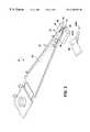
- FIG. 1is a fragmentary perspective view of a data storage system utilizing a read/write head comprised of an optical focusing device according to the present invention
- FIG. 2is a perspective view of a head gimbal assembly comprised of a suspension and a slider to which the read/write head of FIG. 1 is secured, for use in a head stack assembly;
- FIG. 3is an enlarged, schematic, side view of an optical focusing device according to a first embodiment of the present invention for use with data storage systems of FIGS. 1 and 2;
- FIG. 4is a top plan view of an optical substrate illustrating the batch or wafer level production of the optical focusing devices
- FIG. 5is a cross sectional view of the optical substrate of FIG. 4 along line 5 — 5 ;
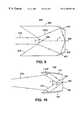
- FIG. 6is a side view of another optical focusing device according to the present invention.
- FIG. 7is a side view of yet another optical focusing device according to the present invention comprised of three complementary components
- FIG. 7Ais a side view of two conical elements forming part of the focusing device of FIG. 7, shown mated to form an axicon;
- FIG. 8is a side view of a still another optical focusing device according to the present invention comprised of two complementary components
- FIG. 8Ais a side view of a complementary conical element forming part of the focusing device of FIG. 8;
- FIG. 9is a side view of a fifth optical focusing device according to the present invention.
- FIG. 10is a side view of a sixth optical focusing device according to the present invention for use with a divergent beam, such as a beam emanating from an optical fiber.
- FIG. 1illustrates a disk drive 10 comprised of a head stack assembly 12 and a stack of spaced apart magnetic data storage disks or media 14 that are rotatable about a common shaft 15 .
- the head stack assembly 12is rotatable about an actuator axis 16 in the direction of the arrow C.
- the head stack assembly 12includes a number of actuator arms, only three of which 18 A, 18 B, 18 C are illustrated, which extend into spacings between the disks 14 .
- the head stack assembly 12further includes an E-shaped block 19 and a magnetic rotor 20 attached to the block 19 in a position diametrically opposite to the actuator arms 18 A, 18 B, 18 C.
- the rotor 20cooperates with a stator (not shown) for rotating in an arc about the actuator axis 16 .
- Energizing a coil of the rotor 20 with a direct current in one polarity or the reverse polaritycauses the head stack assembly 12 , including the actuator arms 18 A, 18 B, 18 C, to rotate about the actuator axis 16 in a direction substantially radial to the disks 14 .
- a head gimbal assembly (HGA) 28is secured to each of the actuator arms, for instance 18 A.
- the HGA 28is comprised of a suspension 33 and a read/write head 35 .
- the suspension 33includes a resilient load beam 36 and a flexure 40 to which the head 35 is secured.
- the head 35is formed of a slider (or slider body) 47 which is secured to the free end of the load beam 36 by means of the flexure 40 , and an optical focusing device (also referred to as near field lens) 50 which is secured to the slider 47 .
- the head 35further includes an optical beam delivery means, such as a waveguide or an optical fiber 48 . Alternatively, the optical beam can be delivered through free space.
- a stationary or a micro-machined dynamic mirror (or another reflective surface) 49 with wires 49 W,can be secured to a trailing edge 55 of the slider 47 at a 45 degree angle relative to the optical beam emanating from the fiber 48 , so as to reflect the optical beam onto the focusing device 50 , in order to transduce data to and from a storage medium 14 (FIG. 3 ).
- the slider 47includes a fiber channel 61 (FIG. 2) for receiving the optical fiber 48 .
- the fiber channel 61is illustrated as being centrally located along a generally central axis of the slider 47 , it should be understood that the location of the fiber channel 61 can be offset relative to a central axis of symmetry of the slider 47 .
- the optical beamcan be transmitted through the fiber channel 61 or a waveguide formed within the fiber channel 61 .
- the focusing device 50is optically transmissive, and is defined by an incident surface 100 , a bottom surface 105 , and a reflective side 110 .
- the incident surface 100is generally flat, and has a preferably circular shape (FIG. 4 ). It should be clear that other shapes can be selected depending on the desired application of the focusing device 50 .
- the bottom surface 105is disposed opposite and parallel to the incident surface 100 , and is similarly generally flat, circularly shaped, and optically transparent.
- the side 110is parabola shaped, and is coated with a reflective layer 120 .
- an incident optical beamsuch as a collimated laser beam 135
- an incident optical beamimpinges upon the incident surface 100 and passes through an optically transmissive body 127 of the focusing device 50 , onto the side 110 .
- the laser beam 135is then reflected by the side 110 as a focused beam 137 through the body 127 onto the bottom surface 105 .
- the focused beam 137impinges upon the bottom surface 105 at a focal spot 162 , as a very small sized spot.
- the focal spot 162is located along a central axis P, in very close proximity to the disk 14 , such that a localized evanescent field or light 170 interacts with the disk 14 , for enabling data to be transduced to and from the disk 14 by effecting near field coupling.
- An electromagnetic coil or coil assembly(not shown), can be formed on the bottom surface 105 , co-axially with the focal spot 162 , for generating a desired write magnetic field.
- the focused beam 137defines an angle of incidence ⁇ with the central axis P. It should be clear that the angle of incidence ⁇ is greater than the angle of incidence had the optical beam 135 not undergone reflection by the side 110 . Consequently, the NA of the focusing device 50 exceeds that of a conventional objective lens, as supported by the following equation:
- nis the index of refraction of the focusing device 50 . It is therefore possible to select the lens body 127 of a material with a high index of refraction n, in order to increase the NA of the focusing device 50 .
- the focusing device 50can be made of any suitable transparent material, including but not limited to glass, crystal, plastic, a combination thereof and so forth.
- the method of manufacturing the focusing device 50will now be described in relation to FIGS. 4 and 5.
- the focusing device 50can be made using molding, etching, or other suitable manufacturing techniques.
- the flatness of the incident surface 100 and the bottom surface 105help facilitate the use of wafer processing in the mass production of the focusing device 50 .
- each focusing device 50can be formed individually, such as by molding, it would be more efficient and economical to mass produce the focusing devices 50 in batches, at wafer level.
- FIG. 4illustrates an optical wafer 200 on which a plurality of substantially identical lens plates 202 are formed.
- Each lens plate 202contains a focusing device 50 .
- the wafer 200can be a flat glass (or silicon) sheet which is etched, molded, or pressed.
- the optical wafer 200is made by etching away openings 215 .
- Each opening 215extends through the entire height of the wafer 200 , and is contoured by a wall 220 having a desired shape that simulates the shape of the side 110 .
- the wall 220is substantially parabola shape.
- the interior of the wall 220is then coated with a reflective layer or coating 120 which is made for example of aluminum, silver, or gold.
- the rest of the opening 215is then filled with a suitable optical material such as high index glass to form the body 127 of the focusing device 50 .
- the top and bottom surfaces 216 , 217 , respectively of the optical wafer 200are lapped to the desired dimensions.
- the overall height “H” of focusing device 50ranges between approximately 200 microns and approximately 600 microns.
- the diameter or width “D” of the incident surface 100ranges between approximately 300 microns and approximately 600 microns.
- the diameter or width “d” of the bottom surface 105ranges between approximately 200 microns and approximately 400 microns.
- the optical wafer 200is sliced into individual lens plates 202 , along lines 233 (shown in dashed lines in FIG. 5 ).
- the lens plate 202facilitates the handling of the focusing device 50 and its assembly to the slider body 47 .
- FIG. 6illustrates another focusing device 300 according to the present invention.
- the focusing device 300is comprised of a focusing device 350 and a complementary conical element 353 .
- the focusing device 350is generally similar in function and design to the focusing device 50 of FIG. 3, and includes an incident surface 100 , a bottom surface 195 and a side 370 .
- the side 370is generally similar in function and design to the side 110 of the focusing device 50 .
- the side 370is parabola shaped.
- ⁇is the rotation angle of the parabola curve
- fis the focus length of the parabola
- ⁇is the cylindrical radius (i.e., the distance to the central axis P).
- the tilted parabola curvatureis selected to cancel or compensate for the first (and/or other) order conical term or terms introduced by the conical element 353 .
- the tilted parabola curvaturefurther provides tight focus of the incoming optical beam.
- the conical element 353is optically transmissive, and includes a flat incident surface 373 , a conical exit surface 375 , and a cylindrical side 378 with a circular cross-section.
- the conical element 353is disposed at a distance “S” from the focusing device 350 , wherein the distance “S” is measured from the apex 380 of the exit surface 375 and the incident surface 100 of the focusing device 350 .
- the apex 380is preferably aligned along the central axis P and the focal spot 162 . In one embodiment, the distance “S” ranges between approximately 200 microns and approximately 500 microns.
- the cone angle “ ⁇ ” of the exit surface 375is defined between the exit surface 375 and the central axis “P”. In one embodiment, the cone angle “ ⁇ ” ranges between approximately 40 degrees and approximately 80 degrees. Other values of the distance “S” and the cone angle “ ⁇ ” can vary with the desired applications.
- an incident optical beamsuch as the collimated laser beam 135
- the exit surface 373refracts the incident beam 135 into a divergent beam 135 A that impinges upon the incident surface 100 of the focusing device 350 .
- the divergent beam 135 Apasses through the optically transmissive body of the focusing device 50 , onto the side 370 , and is reflected thereby as a focused beam onto the bottom surface 105 at the focal spot 162 .
- the advantages of the focusing device 300are: (1) The focusing device 300 has a high NA that translates into a small spot size; and (2) the focusing device 300 offers high optical efficiency. This design offers a high numerical aperture (NA) and ease of manufacture.
- FIG. 7illustrates another focusing device 400 according to the present invention.
- the focusing device 400is comprised of the focusing device 50 (FIG. 3 ), the conical element 353 (FIG. 6 ), and a complementary conical element 425 disposed intermediate the focusing device 50 and the conical element 353 .
- the focusing device 50can be replaced with the focusing device 350 (FIG. 6) or another suitable focusing device or lens.
- the complementary conical element 425is optically transmissive and includes an incident conical surface 475 , a flat exit surface 473 , and a cylindrical side 478 with a circular cross-section.
- the conical element 475is disposed at a distance “S 1 ” from the complementary conical exit surface 375 of the conical element 353 .
- the distance “S 1 ”is measured from the apex 380 of the exit surface 375 of the conical element 353 , and the apex 480 of the conical incident surface 475 of the complementary conical element 425 .
- the distance “S 1 ”ranges approximately 200 microns and approximately 500 microns.
- the apices 380 and 480are preferably disposed colinearly with the focal spot 162 , along the central axis P.
- the cone angle “ ⁇ ” of the incident surface 475is defined between the incident surface 475 and the central axis “P”.
- the cone angle “ ⁇ ” of the incident surface 475is the same as the cone angle “ ⁇ ” of the exit surface 375 , so that the exit surface 375 and the incident surface 475 are complementary.
- the exit surface 375 and the incident surface 475will mate to form a cylindrical axicon whose diameter “H” ranges approximately 200 microns and approximately 500 microns, and whose height “h” ranges between approximately 50 microns and approximately 300 microns. It should be clear that other dimensions can alternatively be selected depending on the desired application.
- the flat incident surface 373 of the conical element 353 and the flat exit surface 473 of the complementary conical element 425are parallel.
- the exit surface 473 of the complementary conical element 425is separated from the incident surface 100 of the focusing device 50 by a distance “S 2 ”.
- the distance “S 2 ”can be selected between approximately 10 microns and approximately 100 microns, and the cone angle “ ⁇ ” can be selected between approximately 40 degrees and approximately 80 degrees.
- an incident optical beamsuch as the collimated laser beam 135 , impinges upon the incident surface 373 and passes through the body of the conical element 353 for impinging onto the conical exit surface 375 .
- the exit surface 375refracts the incident beam 135 into a divergent beam 135 A, which, in turn, impinges upon the incident surface 475 of the complementary conical element 425 .
- the index of refraction (n) of the conical element 353matches that, or is the same as the index of refraction of the complementary conical element 425 .
- the divergent beam 135 Ais refracted by the complementary conical element 425 into a collimated cylindrical beam 135 B.
- the collimated beam 135 Bimpinges upon the side 110 of the focusing device 50 for reflection thereby as a focused beam onto the bottom surface 105 at the focal spot 162 .
- FIG. 8illustrates another focusing device 500 according to the present invention.
- the focusing device 500is comprised of the conical element 353 (FIGS. 6, 7 ) and a complementary conical element 525 .
- the complementary conical element 525is optically transmissive and includes an incident conical surface 575 , a cylindrical side 578 with a circular cross-section, a side 510 with a parabolic curvature, and a flat bottom surface 505 .
- the conical element 353is disposed at a distance “S 3 ” from the complementary conical element 525 .
- the distance “S 3 ”is measured from the apex 380 of the exit surface 375 of the conical element 353 and the apex 580 of the conical incident surface 575 of the complementary conical element 525 .
- the distance “S 3 ”ranges between approximately 200 microns and approximately 500 microns.
- the apices 380 and 580are preferably disposed colinearly with the focal spot 162 , along the central axis P.
- the cone angle “ ⁇ ” of the incident surface 575is defined between the incident surface 575 and the central axis “P”.
- the cone angle “ ⁇ ” of the incident surface 575is the same as the cone angle “ ⁇ ” of the exit surface 375 , so that the exit surface 375 and the incident surface 575 are complementary. In other terms, if both conical elements 353 and 525 were fitted together, the exit surface 375 and the incident surface 575 will mate with tight accuracy.
- FIG. 8Afurther illustrates the complementary conical element 525 as being formed of the complementary conical element 425 (FIG. 7) and the conical focusing device 50 (FIGS. 3, 7 ).
- the interface surfaces of the complementary conical element 425 and the conical focusing device 50are shown outlined by two dashed lines. While the complementary conical element 525 is illustrated as being integral (i.e., made of a single piece), it should be clear that the complementary conical element 525 can be formed of the combination of both the complementary conical element 425 and the conical focusing device 50 , in essence reducing the separation distance S 2 (FIG. 7) to zero or close to zero.
- the separation distance “S 3 ” and the cone angle “ ⁇ ”are selected such that all or substantially all the rays of the laser beam 135 are reflected and focused by the side 510 .
- an incident optical beamsuch as the collimated laser beam 135 , impinges upon the incident surface 373 and passes through the body of the conical element 353 for impinging onto the conical exit surface 375 .
- the exit surface 373refracts the incident beam 135 into a divergent beam 135 A, which, in turn, impinges upon the incident surface 575 of the complementary conical element 525 .
- the index of refraction (n) of the conical element 353matches that, or is the same as the index of refraction of the complementary conical element 525 .
- the divergent beam 135 Ais refracted by the complementary conical element 525 into a collimated cylindrical beam 135 C that impinges upon the parabolic side 510 of the complementary conical element 525 for reflection thereby as a focused beam onto the bottom surface 505 at the focal spot 162 .
- the conical incident surface 575 and its apex 580correspond to the conical incident surface 475 and the apex 480 of the complementary conical element 425 , respectively.
- the cylindrical side 578corresponds to the cylindrical side 478 of the complementary conical element 425 .
- the side 510 and the bottom surface 505correspond to the side 110 and the bottom surface 105 , respectively of the focusing device 50 .
- FIG. 9illustrates yet another focusing device 600 according to the present invention.
- the focusing device 600is optically transmissive, integrally formed, and comprised of an incident symmetric conical surface 675 , a cylindrical side 625 with a circular cross-section, a tilted parabolic side 610 coated with a reflective layer 620 , and a flat bottom surface 605 .
- the cone angle “ ⁇ ” of the incident surface 675ranges between approximately 40 degrees and approximately 80 degrees. It should be clear that other values can alternatively be selected.
- the apex 680 of the incident surface 675is preferably disposed colinearly with the focal spot 162 , along the central axis P.
- a collimated laser beam 135impinges upon the incident surface 675 and is refracted thereby into a divergent beam 135 D.
- the beam 135 Dpasses through the transmissive body of the focusing device 600 and impinges onto the reflective tilted parabolic side 610 , for reflection thereby as a focused beam onto the bottom surface 605 at the focal spot 162 .
- FIG. 10illustrates still another focusing device 700 according to the present invention.
- the focusing device 700is optically transmissive, integrally formed, and comprised of an incident symmetric conical surface 775 , a tilted parabola side 710 coated with a reflective layer 720 , and a flat bottom surface 705 .
- the cone angle “ ⁇ ” of the incident surface 775ranges between approximately 40 degrees and approximately 80 degrees. It should be clear that other values can alternatively be selected.
- the apex 780 of the incident surface 775is preferably disposed colinearly with the focal spot 162 , along the central axis P.
- a divergent laser beam 135impinges upon the incident surface 775 and is refracted thereby into another divergent beam 135 E.
- the beam 135 Epasses through the transmissive body of the focusing device 700 and impinges onto the reflective tilted parabolic side 710 , for reflection thereby as a focused beam onto the bottom surface 705 at the focal spot 162 .
- the geometry, compositions, and dimensions of the elements described hereincan be modified within the scope of the invention and are not intended to be the exclusive. Other modifications can be made when implementing the invention for a particular environment.
- the use of the focusing deviceis not limited to data storage devices, as it can be used in various other optical applications, including but not limited to high resolution microscopy, surface inspection, and medical imaging.
Landscapes
- Physics & Mathematics (AREA)
- Optics & Photonics (AREA)
- Engineering & Computer Science (AREA)
- Chemical & Material Sciences (AREA)
- Nanotechnology (AREA)
- Mathematical Physics (AREA)
- Theoretical Computer Science (AREA)
- Crystallography & Structural Chemistry (AREA)
- Optical Head (AREA)
Abstract
Description

Claims (25)
Priority Applications (1)
| Application Number | Priority Date | Filing Date | Title |
|---|---|---|---|
| US09/338,785US6185051B1 (en) | 1999-06-23 | 1999-06-23 | High numerical aperture optical focusing device for use in data storage systems |
Applications Claiming Priority (1)
| Application Number | Priority Date | Filing Date | Title |
|---|---|---|---|
| US09/338,785US6185051B1 (en) | 1999-06-23 | 1999-06-23 | High numerical aperture optical focusing device for use in data storage systems |
Publications (1)
| Publication Number | Publication Date |
|---|---|
| US6185051B1true US6185051B1 (en) | 2001-02-06 |
Family
ID=23326160
Family Applications (1)
| Application Number | Title | Priority Date | Filing Date |
|---|---|---|---|
| US09/338,785Expired - LifetimeUS6185051B1 (en) | 1999-06-23 | 1999-06-23 | High numerical aperture optical focusing device for use in data storage systems |
Country Status (1)
| Country | Link |
|---|---|
| US (1) | US6185051B1 (en) |
Cited By (159)
| Publication number | Priority date | Publication date | Assignee | Title |
|---|---|---|---|---|
| US20020014575A1 (en)* | 2000-08-04 | 2002-02-07 | Hiroshi Hatano | Solid Immersion mirror and reproducing apparatus |
| US20020176349A1 (en)* | 2001-05-25 | 2002-11-28 | Gibson Gary A. | Data storage medium utilizing directed light beam and near-field optical sources |
| US20030123162A1 (en)* | 2001-12-31 | 2003-07-03 | Texas Instruments Inc. | Integrated TIR prism and lens element |
| US6791935B2 (en) | 2000-02-17 | 2004-09-14 | Minolta Co., Ltd. | Optical head, and optical recording and reproducing apparatus |
| US6980374B1 (en) | 2004-11-12 | 2005-12-27 | Seagate Technology Llc | Solid immersion mirror |
| US20060062126A1 (en)* | 2001-05-25 | 2006-03-23 | Gibson Gary A | System and method for storing data |
| US20060077787A1 (en)* | 2004-10-12 | 2006-04-13 | Itagi Amit V | Phase offset integrated solid immersion mirror and lens for a general phase front |
| US20070152230A1 (en)* | 2006-01-05 | 2007-07-05 | Duong Dung T | Separate optical device for directing light from an LED |
| US20070153368A1 (en)* | 2005-10-03 | 2007-07-05 | The Salk Institute For Biological Studies | Maximal-aperture reflecting objective |
| US20080080166A1 (en)* | 2006-10-02 | 2008-04-03 | Duong Dung T | LED system and method |
| US20080253005A1 (en)* | 2007-04-16 | 2008-10-16 | Young Optics Inc. | Illumination system |
| US20090275157A1 (en)* | 2006-10-02 | 2009-11-05 | Illumitex, Inc. | Optical device shaping |
| US20090275266A1 (en)* | 2006-10-02 | 2009-11-05 | Illumitex, Inc. | Optical device polishing |
| US20090289263A1 (en)* | 2008-02-08 | 2009-11-26 | Illumitex, Inc. | System and Method for Emitter Layer Shaping |
| US20100128578A1 (en)* | 1998-11-09 | 2010-05-27 | Kenji Kato | Near-field optical head having tapered hole for guiding light beam |
| US20100148193A1 (en)* | 2008-12-11 | 2010-06-17 | Illumitex, Inc. | Systems and methods for packaging light-emitting diode devices |
| US20110044022A1 (en)* | 2009-08-20 | 2011-02-24 | Illumitex, Inc. | System and method for a phosphor coated lens |
| US8585253B2 (en) | 2009-08-20 | 2013-11-19 | Illumitex, Inc. | System and method for color mixing lens array |
| US8830628B1 (en) | 2009-02-23 | 2014-09-09 | Western Digital (Fremont), Llc | Method and system for providing a perpendicular magnetic recording head |
| US8879207B1 (en) | 2011-12-20 | 2014-11-04 | Western Digital (Fremont), Llc | Method for providing a side shield for a magnetic recording transducer using an air bridge |
| US8883017B1 (en) | 2013-03-12 | 2014-11-11 | Western Digital (Fremont), Llc | Method and system for providing a read transducer having seamless interfaces |
| US8917581B1 (en) | 2013-12-18 | 2014-12-23 | Western Digital Technologies, Inc. | Self-anneal process for a near field transducer and chimney in a hard disk drive assembly |
| US8923102B1 (en) | 2013-07-16 | 2014-12-30 | Western Digital (Fremont), Llc | Optical grating coupling for interferometric waveguides in heat assisted magnetic recording heads |
| US8947985B1 (en) | 2013-07-16 | 2015-02-03 | Western Digital (Fremont), Llc | Heat assisted magnetic recording transducers having a recessed pole |
| US8953422B1 (en) | 2014-06-10 | 2015-02-10 | Western Digital (Fremont), Llc | Near field transducer using dielectric waveguide core with fine ridge feature |
| US8958272B1 (en) | 2014-06-10 | 2015-02-17 | Western Digital (Fremont), Llc | Interfering near field transducer for energy assisted magnetic recording |
| US8971160B1 (en) | 2013-12-19 | 2015-03-03 | Western Digital (Fremont), Llc | Near field transducer with high refractive index pin for heat assisted magnetic recording |
| US8970988B1 (en) | 2013-12-31 | 2015-03-03 | Western Digital (Fremont), Llc | Electric gaps and method for making electric gaps for multiple sensor arrays |
| US8976635B1 (en) | 2014-06-10 | 2015-03-10 | Western Digital (Fremont), Llc | Near field transducer driven by a transverse electric waveguide for energy assisted magnetic recording |
| US8980109B1 (en) | 2012-12-11 | 2015-03-17 | Western Digital (Fremont), Llc | Method for providing a magnetic recording transducer using a combined main pole and side shield CMP for a wraparound shield scheme |
| US8982508B1 (en) | 2011-10-31 | 2015-03-17 | Western Digital (Fremont), Llc | Method for providing a side shield for a magnetic recording transducer |
| US8988825B1 (en) | 2014-02-28 | 2015-03-24 | Western Digital (Fremont, LLC | Method for fabricating a magnetic writer having half-side shields |
| US8984740B1 (en) | 2012-11-30 | 2015-03-24 | Western Digital (Fremont), Llc | Process for providing a magnetic recording transducer having a smooth magnetic seed layer |
| US8988812B1 (en) | 2013-11-27 | 2015-03-24 | Western Digital (Fremont), Llc | Multi-sensor array configuration for a two-dimensional magnetic recording (TDMR) operation |
| US8995087B1 (en) | 2006-11-29 | 2015-03-31 | Western Digital (Fremont), Llc | Perpendicular magnetic recording write head having a wrap around shield |
| US8993217B1 (en) | 2013-04-04 | 2015-03-31 | Western Digital (Fremont), Llc | Double exposure technique for high resolution disk imaging |
| US8997832B1 (en) | 2010-11-23 | 2015-04-07 | Western Digital (Fremont), Llc | Method of fabricating micrometer scale components |
| US9001467B1 (en) | 2014-03-05 | 2015-04-07 | Western Digital (Fremont), Llc | Method for fabricating side shields in a magnetic writer |
| US9001628B1 (en) | 2013-12-16 | 2015-04-07 | Western Digital (Fremont), Llc | Assistant waveguides for evaluating main waveguide coupling efficiency and diode laser alignment tolerances for hard disk |
| US9007719B1 (en) | 2013-10-23 | 2015-04-14 | Western Digital (Fremont), Llc | Systems and methods for using double mask techniques to achieve very small features |
| US9007879B1 (en) | 2014-06-10 | 2015-04-14 | Western Digital (Fremont), Llc | Interfering near field transducer having a wide metal bar feature for energy assisted magnetic recording |
| US9007725B1 (en) | 2014-10-07 | 2015-04-14 | Western Digital (Fremont), Llc | Sensor with positive coupling between dual ferromagnetic free layer laminates |
| US9013836B1 (en) | 2013-04-02 | 2015-04-21 | Western Digital (Fremont), Llc | Method and system for providing an antiferromagnetically coupled return pole |
| US9042208B1 (en) | 2013-03-11 | 2015-05-26 | Western Digital Technologies, Inc. | Disk drive measuring fly height by applying a bias voltage to an electrically insulated write component of a head |
| US9042057B1 (en) | 2013-01-09 | 2015-05-26 | Western Digital (Fremont), Llc | Methods for providing magnetic storage elements with high magneto-resistance using Heusler alloys |
| US9042051B2 (en) | 2013-08-15 | 2015-05-26 | Western Digital (Fremont), Llc | Gradient write gap for perpendicular magnetic recording writer |
| US9042052B1 (en) | 2014-06-23 | 2015-05-26 | Western Digital (Fremont), Llc | Magnetic writer having a partially shunted coil |
| US9042058B1 (en) | 2013-10-17 | 2015-05-26 | Western Digital Technologies, Inc. | Shield designed for middle shields in a multiple sensor array |
| US9046241B2 (en) | 2011-11-12 | 2015-06-02 | Jingqun Xi | High efficiency directional light source using lens optics |
| US9053735B1 (en) | 2014-06-20 | 2015-06-09 | Western Digital (Fremont), Llc | Method for fabricating a magnetic writer using a full-film metal planarization |
| US9064507B1 (en) | 2009-07-31 | 2015-06-23 | Western Digital (Fremont), Llc | Magnetic etch-stop layer for magnetoresistive read heads |
| US9064528B1 (en) | 2013-05-17 | 2015-06-23 | Western Digital Technologies, Inc. | Interferometric waveguide usable in shingled heat assisted magnetic recording in the absence of a near-field transducer |
| US9064527B1 (en) | 2013-04-12 | 2015-06-23 | Western Digital (Fremont), Llc | High order tapered waveguide for use in a heat assisted magnetic recording head |
| US9065043B1 (en) | 2012-06-29 | 2015-06-23 | Western Digital (Fremont), Llc | Tunnel magnetoresistance read head with narrow shield-to-shield spacing |
| US9070381B1 (en) | 2013-04-12 | 2015-06-30 | Western Digital (Fremont), Llc | Magnetic recording read transducer having a laminated free layer |
| US9082423B1 (en) | 2013-12-18 | 2015-07-14 | Western Digital (Fremont), Llc | Magnetic recording write transducer having an improved trailing surface profile |
| US9087534B1 (en) | 2011-12-20 | 2015-07-21 | Western Digital (Fremont), Llc | Method and system for providing a read transducer having soft and hard magnetic bias structures |
| US9087527B1 (en) | 2014-10-28 | 2015-07-21 | Western Digital (Fremont), Llc | Apparatus and method for middle shield connection in magnetic recording transducers |
| US9093639B2 (en) | 2012-02-21 | 2015-07-28 | Western Digital (Fremont), Llc | Methods for manufacturing a magnetoresistive structure utilizing heating and cooling |
| US9104107B1 (en) | 2013-04-03 | 2015-08-11 | Western Digital (Fremont), Llc | DUV photoresist process |
| US9111558B1 (en) | 2014-03-14 | 2015-08-18 | Western Digital (Fremont), Llc | System and method of diffractive focusing of light in a waveguide |
| US9111564B1 (en) | 2013-04-02 | 2015-08-18 | Western Digital (Fremont), Llc | Magnetic recording writer having a main pole with multiple flare angles |
| US9111550B1 (en) | 2014-12-04 | 2015-08-18 | Western Digital (Fremont), Llc | Write transducer having a magnetic buffer layer spaced between a side shield and a write pole by non-magnetic layers |
| US9123358B1 (en) | 2012-06-11 | 2015-09-01 | Western Digital (Fremont), Llc | Conformal high moment side shield seed layer for perpendicular magnetic recording writer |
| US9123374B1 (en) | 2015-02-12 | 2015-09-01 | Western Digital (Fremont), Llc | Heat assisted magnetic recording writer having an integrated polarization rotation plate |
| US9123359B1 (en) | 2010-12-22 | 2015-09-01 | Western Digital (Fremont), Llc | Magnetic recording transducer with sputtered antiferromagnetic coupling trilayer between plated ferromagnetic shields and method of fabrication |
| US9123362B1 (en) | 2011-03-22 | 2015-09-01 | Western Digital (Fremont), Llc | Methods for assembling an electrically assisted magnetic recording (EAMR) head |
| US9135930B1 (en) | 2014-03-06 | 2015-09-15 | Western Digital (Fremont), Llc | Method for fabricating a magnetic write pole using vacuum deposition |
| US9135937B1 (en) | 2014-05-09 | 2015-09-15 | Western Digital (Fremont), Llc | Current modulation on laser diode for energy assisted magnetic recording transducer |
| US9142233B1 (en) | 2014-02-28 | 2015-09-22 | Western Digital (Fremont), Llc | Heat assisted magnetic recording writer having a recessed pole |
| US9147404B1 (en) | 2015-03-31 | 2015-09-29 | Western Digital (Fremont), Llc | Method and system for providing a read transducer having a dual free layer |
| US9147408B1 (en) | 2013-12-19 | 2015-09-29 | Western Digital (Fremont), Llc | Heated AFM layer deposition and cooling process for TMR magnetic recording sensor with high pinning field |
| US9153255B1 (en) | 2014-03-05 | 2015-10-06 | Western Digital (Fremont), Llc | Method for fabricating a magnetic writer having an asymmetric gap and shields |
| US9183854B2 (en) | 2014-02-24 | 2015-11-10 | Western Digital (Fremont), Llc | Method to make interferometric taper waveguide for HAMR light delivery |
| US9190079B1 (en) | 2014-09-22 | 2015-11-17 | Western Digital (Fremont), Llc | Magnetic write pole having engineered radius of curvature and chisel angle profiles |
| US9190085B1 (en) | 2014-03-12 | 2015-11-17 | Western Digital (Fremont), Llc | Waveguide with reflective grating for localized energy intensity |
| US9194692B1 (en) | 2013-12-06 | 2015-11-24 | Western Digital (Fremont), Llc | Systems and methods for using white light interferometry to measure undercut of a bi-layer structure |
| US9202480B2 (en) | 2009-10-14 | 2015-12-01 | Western Digital (Fremont), LLC. | Double patterning hard mask for damascene perpendicular magnetic recording (PMR) writer |
| US9202493B1 (en) | 2014-02-28 | 2015-12-01 | Western Digital (Fremont), Llc | Method of making an ultra-sharp tip mode converter for a HAMR head |
| US9214169B1 (en) | 2014-06-20 | 2015-12-15 | Western Digital (Fremont), Llc | Magnetic recording read transducer having a laminated free layer |
| US9213322B1 (en) | 2012-08-16 | 2015-12-15 | Western Digital (Fremont), Llc | Methods for providing run to run process control using a dynamic tuner |
| US9214165B1 (en) | 2014-12-18 | 2015-12-15 | Western Digital (Fremont), Llc | Magnetic writer having a gradient in saturation magnetization of the shields |
| US9214172B2 (en) | 2013-10-23 | 2015-12-15 | Western Digital (Fremont), Llc | Method of manufacturing a magnetic read head |
| US9230565B1 (en) | 2014-06-24 | 2016-01-05 | Western Digital (Fremont), Llc | Magnetic shield for magnetic recording head |
| US9236560B1 (en) | 2014-12-08 | 2016-01-12 | Western Digital (Fremont), Llc | Spin transfer torque tunneling magnetoresistive device having a laminated free layer with perpendicular magnetic anisotropy |
| US9245543B1 (en) | 2010-06-25 | 2016-01-26 | Western Digital (Fremont), Llc | Method for providing an energy assisted magnetic recording head having a laser integrally mounted to the slider |
| US9245545B1 (en) | 2013-04-12 | 2016-01-26 | Wester Digital (Fremont), Llc | Short yoke length coils for magnetic heads in disk drives |
| US9245562B1 (en) | 2015-03-30 | 2016-01-26 | Western Digital (Fremont), Llc | Magnetic recording writer with a composite main pole |
| US9251813B1 (en) | 2009-04-19 | 2016-02-02 | Western Digital (Fremont), Llc | Method of making a magnetic recording head |
| US9263071B1 (en) | 2015-03-31 | 2016-02-16 | Western Digital (Fremont), Llc | Flat NFT for heat assisted magnetic recording |
| US9263067B1 (en) | 2013-05-29 | 2016-02-16 | Western Digital (Fremont), Llc | Process for making PMR writer with constant side wall angle |
| US9269382B1 (en) | 2012-06-29 | 2016-02-23 | Western Digital (Fremont), Llc | Method and system for providing a read transducer having improved pinning of the pinned layer at higher recording densities |
| US9275657B1 (en) | 2013-08-14 | 2016-03-01 | Western Digital (Fremont), Llc | Process for making PMR writer with non-conformal side gaps |
| US9280990B1 (en) | 2013-12-11 | 2016-03-08 | Western Digital (Fremont), Llc | Method for fabricating a magnetic writer using multiple etches |
| US9287494B1 (en) | 2013-06-28 | 2016-03-15 | Western Digital (Fremont), Llc | Magnetic tunnel junction (MTJ) with a magnesium oxide tunnel barrier |
| US9286919B1 (en) | 2014-12-17 | 2016-03-15 | Western Digital (Fremont), Llc | Magnetic writer having a dual side gap |
| US9305583B1 (en) | 2014-02-18 | 2016-04-05 | Western Digital (Fremont), Llc | Method for fabricating a magnetic writer using multiple etches of damascene materials |
| US9312064B1 (en) | 2015-03-02 | 2016-04-12 | Western Digital (Fremont), Llc | Method to fabricate a magnetic head including ion milling of read gap using dual layer hard mask |
| US9318130B1 (en) | 2013-07-02 | 2016-04-19 | Western Digital (Fremont), Llc | Method to fabricate tunneling magnetic recording heads with extended pinned layer |
| US9336814B1 (en) | 2013-03-12 | 2016-05-10 | Western Digital (Fremont), Llc | Inverse tapered waveguide for use in a heat assisted magnetic recording head |
| US9343087B1 (en) | 2014-12-21 | 2016-05-17 | Western Digital (Fremont), Llc | Method for fabricating a magnetic writer having half shields |
| US9343086B1 (en) | 2013-09-11 | 2016-05-17 | Western Digital (Fremont), Llc | Magnetic recording write transducer having an improved sidewall angle profile |
| US9343098B1 (en) | 2013-08-23 | 2016-05-17 | Western Digital (Fremont), Llc | Method for providing a heat assisted magnetic recording transducer having protective pads |
| US9349394B1 (en) | 2013-10-18 | 2016-05-24 | Western Digital (Fremont), Llc | Method for fabricating a magnetic writer having a gradient side gap |
| US9349392B1 (en) | 2012-05-24 | 2016-05-24 | Western Digital (Fremont), Llc | Methods for improving adhesion on dielectric substrates |
| US9361914B1 (en) | 2014-06-18 | 2016-06-07 | Western Digital (Fremont), Llc | Magnetic sensor with thin capping layer |
| US9361913B1 (en) | 2013-06-03 | 2016-06-07 | Western Digital (Fremont), Llc | Recording read heads with a multi-layer AFM layer methods and apparatuses |
| US9368134B1 (en) | 2010-12-16 | 2016-06-14 | Western Digital (Fremont), Llc | Method and system for providing an antiferromagnetically coupled writer |
| US9384763B1 (en) | 2015-03-26 | 2016-07-05 | Western Digital (Fremont), Llc | Dual free layer magnetic reader having a rear bias structure including a soft bias layer |
| US9384765B1 (en) | 2015-09-24 | 2016-07-05 | Western Digital (Fremont), Llc | Method and system for providing a HAMR writer having improved optical efficiency |
| US9396743B1 (en) | 2014-02-28 | 2016-07-19 | Western Digital (Fremont), Llc | Systems and methods for controlling soft bias thickness for tunnel magnetoresistance readers |
| US9396742B1 (en) | 2012-11-30 | 2016-07-19 | Western Digital (Fremont), Llc | Magnetoresistive sensor for a magnetic storage system read head, and fabrication method thereof |
| US9406331B1 (en) | 2013-06-17 | 2016-08-02 | Western Digital (Fremont), Llc | Method for making ultra-narrow read sensor and read transducer device resulting therefrom |
| US9424866B1 (en) | 2015-09-24 | 2016-08-23 | Western Digital (Fremont), Llc | Heat assisted magnetic recording write apparatus having a dielectric gap |
| US9431039B1 (en) | 2013-05-21 | 2016-08-30 | Western Digital (Fremont), Llc | Multiple sensor array usable in two-dimensional magnetic recording |
| US9431031B1 (en) | 2015-03-24 | 2016-08-30 | Western Digital (Fremont), Llc | System and method for magnetic transducers having multiple sensors and AFC shields |
| US9431038B1 (en) | 2015-06-29 | 2016-08-30 | Western Digital (Fremont), Llc | Method for fabricating a magnetic write pole having an improved sidewall angle profile |
| US9431047B1 (en) | 2013-05-01 | 2016-08-30 | Western Digital (Fremont), Llc | Method for providing an improved AFM reader shield |
| US9431032B1 (en) | 2013-08-14 | 2016-08-30 | Western Digital (Fremont), Llc | Electrical connection arrangement for a multiple sensor array usable in two-dimensional magnetic recording |
| US9437251B1 (en) | 2014-12-22 | 2016-09-06 | Western Digital (Fremont), Llc | Apparatus and method having TDMR reader to reader shunts |
| US9441938B1 (en) | 2013-10-08 | 2016-09-13 | Western Digital (Fremont), Llc | Test structures for measuring near field transducer disc length |
| US9443541B1 (en) | 2015-03-24 | 2016-09-13 | Western Digital (Fremont), Llc | Magnetic writer having a gradient in saturation magnetization of the shields and return pole |
| US9449625B1 (en) | 2014-12-24 | 2016-09-20 | Western Digital (Fremont), Llc | Heat assisted magnetic recording head having a plurality of diffusion barrier layers |
| US9449621B1 (en) | 2015-03-26 | 2016-09-20 | Western Digital (Fremont), Llc | Dual free layer magnetic reader having a rear bias structure having a high aspect ratio |
| US9472216B1 (en) | 2015-09-23 | 2016-10-18 | Western Digital (Fremont), Llc | Differential dual free layer magnetic reader |
| US9484051B1 (en) | 2015-11-09 | 2016-11-01 | The Provost, Fellows, Foundation Scholars and the other members of Board, of the College of the Holy and Undivided Trinity of Queen Elizabeth near Dublin | Method and system for reducing undesirable reflections in a HAMR write apparatus |
| US9508372B1 (en) | 2015-06-03 | 2016-11-29 | Western Digital (Fremont), Llc | Shingle magnetic writer having a low sidewall angle pole |
| US9508365B1 (en) | 2015-06-24 | 2016-11-29 | Western Digital (Fremont), LLC. | Magnetic reader having a crystal decoupling structure |
| US9508363B1 (en) | 2014-06-17 | 2016-11-29 | Western Digital (Fremont), Llc | Method for fabricating a magnetic write pole having a leading edge bevel |
| US9530443B1 (en) | 2015-06-25 | 2016-12-27 | Western Digital (Fremont), Llc | Method for fabricating a magnetic recording device having a high aspect ratio structure |
| US9564150B1 (en) | 2015-11-24 | 2017-02-07 | Western Digital (Fremont), Llc | Magnetic read apparatus having an improved read sensor isolation circuit |
| US9595273B1 (en) | 2015-09-30 | 2017-03-14 | Western Digital (Fremont), Llc | Shingle magnetic writer having nonconformal shields |
| US9646639B2 (en) | 2015-06-26 | 2017-05-09 | Western Digital (Fremont), Llc | Heat assisted magnetic recording writer having integrated polarization rotation waveguides |
| US9666214B1 (en) | 2015-09-23 | 2017-05-30 | Western Digital (Fremont), Llc | Free layer magnetic reader that may have a reduced shield-to-shield spacing |
| US20170189991A1 (en)* | 2014-07-14 | 2017-07-06 | Corning Incorporated | Systems and methods for processing transparent materials using adjustable laser beam focal lines |
| US9721595B1 (en) | 2014-12-04 | 2017-08-01 | Western Digital (Fremont), Llc | Method for providing a storage device |
| US9741366B1 (en) | 2014-12-18 | 2017-08-22 | Western Digital (Fremont), Llc | Method for fabricating a magnetic writer having a gradient in saturation magnetization of the shields |
| US9740805B1 (en) | 2015-12-01 | 2017-08-22 | Western Digital (Fremont), Llc | Method and system for detecting hotspots for photolithographically-defined devices |
| US9754611B1 (en) | 2015-11-30 | 2017-09-05 | Western Digital (Fremont), Llc | Magnetic recording write apparatus having a stepped conformal trailing shield |
| US9767831B1 (en) | 2015-12-01 | 2017-09-19 | Western Digital (Fremont), Llc | Magnetic writer having convex trailing surface pole and conformal write gap |
| US9786301B1 (en) | 2014-12-02 | 2017-10-10 | Western Digital (Fremont), Llc | Apparatuses and methods for providing thin shields in a multiple sensor array |
| US9799351B1 (en) | 2015-11-30 | 2017-10-24 | Western Digital (Fremont), Llc | Short yoke length writer having assist coils |
| US9812155B1 (en) | 2015-11-23 | 2017-11-07 | Western Digital (Fremont), Llc | Method and system for fabricating high junction angle read sensors |
| US9842615B1 (en) | 2015-06-26 | 2017-12-12 | Western Digital (Fremont), Llc | Magnetic reader having a nonmagnetic insertion layer for the pinning layer |
| US9858951B1 (en) | 2015-12-01 | 2018-01-02 | Western Digital (Fremont), Llc | Method for providing a multilayer AFM layer in a read sensor |
| US9881638B1 (en) | 2014-12-17 | 2018-01-30 | Western Digital (Fremont), Llc | Method for providing a near-field transducer (NFT) for a heat assisted magnetic recording (HAMR) device |
| US9934811B1 (en) | 2014-03-07 | 2018-04-03 | Western Digital (Fremont), Llc | Methods for controlling stray fields of magnetic features using magneto-elastic anisotropy |
| US9953670B1 (en) | 2015-11-10 | 2018-04-24 | Western Digital (Fremont), Llc | Method and system for providing a HAMR writer including a multi-mode interference device |
| US10037770B1 (en) | 2015-11-12 | 2018-07-31 | Western Digital (Fremont), Llc | Method for providing a magnetic recording write apparatus having a seamless pole |
| US10074387B1 (en) | 2014-12-21 | 2018-09-11 | Western Digital (Fremont), Llc | Method and system for providing a read transducer having symmetric antiferromagnetically coupled shields |
| RU2685573C1 (en)* | 2018-07-04 | 2019-04-22 | АКЦИОНЕРНОЕ ОБЩЕСТВО "Научно-исследовательский институт оптико-электронного приборостроения" (АО "НИИ ОЭП") | Method of focusing optical radiation on object |
| US11130701B2 (en) | 2016-09-30 | 2021-09-28 | Corning Incorporated | Apparatuses and methods for laser processing transparent workpieces using non-axisymmetric beam spots |
| US11148225B2 (en) | 2013-12-17 | 2021-10-19 | Corning Incorporated | Method for rapid laser drilling of holes in glass and products made therefrom |
| US11345625B2 (en) | 2013-01-15 | 2022-05-31 | Corning Laser Technologies GmbH | Method and device for the laser-based machining of sheet-like substrates |
| US11542190B2 (en) | 2016-10-24 | 2023-01-03 | Corning Incorporated | Substrate processing station for laser-based machining of sheet-like glass substrates |
| US11556039B2 (en) | 2013-12-17 | 2023-01-17 | Corning Incorporated | Electrochromic coated glass articles and methods for laser processing the same |
| US11697178B2 (en) | 2014-07-08 | 2023-07-11 | Corning Incorporated | Methods and apparatuses for laser processing materials |
| US11713271B2 (en) | 2013-03-21 | 2023-08-01 | Corning Laser Technologies GmbH | Device and method for cutting out contours from planar substrates by means of laser |
| US11773004B2 (en) | 2015-03-24 | 2023-10-03 | Corning Incorporated | Laser cutting and processing of display glass compositions |
Citations (8)
| Publication number | Priority date | Publication date | Assignee | Title |
|---|---|---|---|---|
| US3999855A (en)* | 1974-10-24 | 1976-12-28 | Block Engineering, Inc. | Illumination system |
| US5042928A (en) | 1990-02-20 | 1991-08-27 | Eastman Kodak Company | Parallel catadioptric optical element |
| US5125750A (en) | 1991-03-14 | 1992-06-30 | The Board Of Trustees Of The Leland Stanford Junior University | Optical recording system employing a solid immersion lens |
| US5285318A (en)* | 1992-06-22 | 1994-02-08 | Nioptics Corporation | Illumination system having an aspherical lens |
| US5497359A (en) | 1994-08-30 | 1996-03-05 | National Business Machines Corporation | Optical disk data storage system with radiation-transparent air-bearing slider |
| EP0758753A2 (en) | 1995-08-16 | 1997-02-19 | Eastman Kodak Company | Diffractive optical elements |
| US5689480A (en) | 1996-08-13 | 1997-11-18 | The Board Of Trustees Of The Leland Stanford Junior University | Magneto-optic recording system employing near field optics |
| US5986995A (en)* | 1998-07-06 | 1999-11-16 | Read-Rite Corporation | High NA catadioptric focusing device having flat diffractive surfaces |
- 1999
- 1999-06-23USUS09/338,785patent/US6185051B1/ennot_activeExpired - Lifetime
Patent Citations (8)
| Publication number | Priority date | Publication date | Assignee | Title |
|---|---|---|---|---|
| US3999855A (en)* | 1974-10-24 | 1976-12-28 | Block Engineering, Inc. | Illumination system |
| US5042928A (en) | 1990-02-20 | 1991-08-27 | Eastman Kodak Company | Parallel catadioptric optical element |
| US5125750A (en) | 1991-03-14 | 1992-06-30 | The Board Of Trustees Of The Leland Stanford Junior University | Optical recording system employing a solid immersion lens |
| US5285318A (en)* | 1992-06-22 | 1994-02-08 | Nioptics Corporation | Illumination system having an aspherical lens |
| US5497359A (en) | 1994-08-30 | 1996-03-05 | National Business Machines Corporation | Optical disk data storage system with radiation-transparent air-bearing slider |
| EP0758753A2 (en) | 1995-08-16 | 1997-02-19 | Eastman Kodak Company | Diffractive optical elements |
| US5689480A (en) | 1996-08-13 | 1997-11-18 | The Board Of Trustees Of The Leland Stanford Junior University | Magneto-optic recording system employing near field optics |
| US5986995A (en)* | 1998-07-06 | 1999-11-16 | Read-Rite Corporation | High NA catadioptric focusing device having flat diffractive surfaces |
Non-Patent Citations (2)
| Title |
|---|
| Lee, C.W., et al., "Feasibility Study on Near Field Optical Memory Using A Catadioptric Optical System", Optical Data Storage, Technical Digest Series, vol. 8, pp. 137-139, May 10-13, 1998. |
| Mansipur, M. et al. "Parallel Processing", 42 Optics and Photonics News, pp. 42-45, Jun. 1998. |
Cited By (198)
| Publication number | Priority date | Publication date | Assignee | Title |
|---|---|---|---|---|
| US20100128578A1 (en)* | 1998-11-09 | 2010-05-27 | Kenji Kato | Near-field optical head having tapered hole for guiding light beam |
| US8320228B2 (en)* | 1998-11-09 | 2012-11-27 | Seiko Instruments Inc. | Near-field optical head having tapered hole for guiding light beam |
| US6791935B2 (en) | 2000-02-17 | 2004-09-14 | Minolta Co., Ltd. | Optical head, and optical recording and reproducing apparatus |
| US20020014575A1 (en)* | 2000-08-04 | 2002-02-07 | Hiroshi Hatano | Solid Immersion mirror and reproducing apparatus |
| US6707026B2 (en)* | 2000-08-04 | 2004-03-16 | Minolta Co., Ltd. | Solid immersion mirror and reproducing apparatus |
| US6970413B2 (en) | 2001-05-25 | 2005-11-29 | Hewlett-Packard Development Company, L.P. | Data storage medium utilizing directed light beam and near-field optical sources |
| US20060062126A1 (en)* | 2001-05-25 | 2006-03-23 | Gibson Gary A | System and method for storing data |
| US7082095B2 (en) | 2001-05-25 | 2006-07-25 | Hewlett-Packard Development Company, L.P. | System and method for storing data |
| US20020176349A1 (en)* | 2001-05-25 | 2002-11-28 | Gibson Gary A. | Data storage medium utilizing directed light beam and near-field optical sources |
| US6961194B2 (en)* | 2001-12-31 | 2005-11-01 | Texas Instruments Incorporated | Integrated TIR prism and lens element |
| US20030123162A1 (en)* | 2001-12-31 | 2003-07-03 | Texas Instruments Inc. | Integrated TIR prism and lens element |
| US20060077787A1 (en)* | 2004-10-12 | 2006-04-13 | Itagi Amit V | Phase offset integrated solid immersion mirror and lens for a general phase front |
| US7567387B2 (en)* | 2004-10-12 | 2009-07-28 | Seagate Technology Llc | Phase offset integrated solid immersion mirror and lens for a general phase front |
| US6980374B1 (en) | 2004-11-12 | 2005-12-27 | Seagate Technology Llc | Solid immersion mirror |
| US20070153368A1 (en)* | 2005-10-03 | 2007-07-05 | The Salk Institute For Biological Studies | Maximal-aperture reflecting objective |
| US7643226B2 (en)* | 2005-10-03 | 2010-01-05 | Salk Institute For Biological Studies | Maximal-aperture reflecting objective |
| US7772604B2 (en) | 2006-01-05 | 2010-08-10 | Illumitex | Separate optical device for directing light from an LED |
| US20070152230A1 (en)* | 2006-01-05 | 2007-07-05 | Duong Dung T | Separate optical device for directing light from an LED |
| US8896003B2 (en) | 2006-01-05 | 2014-11-25 | Illumitex, Inc. | Separate optical device for directing light from an LED |
| US9574743B2 (en) | 2006-01-05 | 2017-02-21 | Illumitex, Inc. | Separate optical device for directing light from an LED |
| US7968896B2 (en) | 2006-01-05 | 2011-06-28 | Illumitex, Inc. | Separate optical device for directing light from an LED |
| US20090275157A1 (en)* | 2006-10-02 | 2009-11-05 | Illumitex, Inc. | Optical device shaping |
| US20090275266A1 (en)* | 2006-10-02 | 2009-11-05 | Illumitex, Inc. | Optical device polishing |
| US20080080166A1 (en)* | 2006-10-02 | 2008-04-03 | Duong Dung T | LED system and method |
| US20080081531A1 (en)* | 2006-10-02 | 2008-04-03 | Duong Dung T | LED system and method |
| US7789531B2 (en) | 2006-10-02 | 2010-09-07 | Illumitex, Inc. | LED system and method |
| US8087960B2 (en) | 2006-10-02 | 2012-01-03 | Illumitex, Inc. | LED system and method |
| US8995087B1 (en) | 2006-11-29 | 2015-03-31 | Western Digital (Fremont), Llc | Perpendicular magnetic recording write head having a wrap around shield |
| US7995298B2 (en)* | 2007-04-16 | 2011-08-09 | Young Optics Inc. | Illumination system |
| US8116019B2 (en)* | 2007-04-16 | 2012-02-14 | Young Optics Inc. | Illumination system |
| US20080253005A1 (en)* | 2007-04-16 | 2008-10-16 | Young Optics Inc. | Illumination system |
| US20090289263A1 (en)* | 2008-02-08 | 2009-11-26 | Illumitex, Inc. | System and Method for Emitter Layer Shaping |
| US8263993B2 (en) | 2008-02-08 | 2012-09-11 | Illumitex, Inc. | System and method for emitter layer shaping |
| US7829358B2 (en) | 2008-02-08 | 2010-11-09 | Illumitex, Inc. | System and method for emitter layer shaping |
| US20100270560A1 (en)* | 2008-02-08 | 2010-10-28 | Duong Dung T | System and method for emitter layer shaping |
| US20100148193A1 (en)* | 2008-12-11 | 2010-06-17 | Illumitex, Inc. | Systems and methods for packaging light-emitting diode devices |
| US8115217B2 (en) | 2008-12-11 | 2012-02-14 | Illumitex, Inc. | Systems and methods for packaging light-emitting diode devices |
| US8830628B1 (en) | 2009-02-23 | 2014-09-09 | Western Digital (Fremont), Llc | Method and system for providing a perpendicular magnetic recording head |
| US9251813B1 (en) | 2009-04-19 | 2016-02-02 | Western Digital (Fremont), Llc | Method of making a magnetic recording head |
| US9064507B1 (en) | 2009-07-31 | 2015-06-23 | Western Digital (Fremont), Llc | Magnetic etch-stop layer for magnetoresistive read heads |
| US20110044022A1 (en)* | 2009-08-20 | 2011-02-24 | Illumitex, Inc. | System and method for a phosphor coated lens |
| US8585253B2 (en) | 2009-08-20 | 2013-11-19 | Illumitex, Inc. | System and method for color mixing lens array |
| US8449128B2 (en) | 2009-08-20 | 2013-05-28 | Illumitex, Inc. | System and method for a lens and phosphor layer |
| US9086211B2 (en) | 2009-08-20 | 2015-07-21 | Illumitex, Inc. | System and method for color mixing lens array |
| US9202480B2 (en) | 2009-10-14 | 2015-12-01 | Western Digital (Fremont), LLC. | Double patterning hard mask for damascene perpendicular magnetic recording (PMR) writer |
| US9245543B1 (en) | 2010-06-25 | 2016-01-26 | Western Digital (Fremont), Llc | Method for providing an energy assisted magnetic recording head having a laser integrally mounted to the slider |
| US9672847B2 (en) | 2010-11-23 | 2017-06-06 | Western Digital (Fremont), Llc | Micrometer scale components |
| US9159345B1 (en) | 2010-11-23 | 2015-10-13 | Western Digital (Fremont), Llc | Micrometer scale components |
| US8997832B1 (en) | 2010-11-23 | 2015-04-07 | Western Digital (Fremont), Llc | Method of fabricating micrometer scale components |
| US9368134B1 (en) | 2010-12-16 | 2016-06-14 | Western Digital (Fremont), Llc | Method and system for providing an antiferromagnetically coupled writer |
| US9123359B1 (en) | 2010-12-22 | 2015-09-01 | Western Digital (Fremont), Llc | Magnetic recording transducer with sputtered antiferromagnetic coupling trilayer between plated ferromagnetic shields and method of fabrication |
| US9123362B1 (en) | 2011-03-22 | 2015-09-01 | Western Digital (Fremont), Llc | Methods for assembling an electrically assisted magnetic recording (EAMR) head |
| US8982508B1 (en) | 2011-10-31 | 2015-03-17 | Western Digital (Fremont), Llc | Method for providing a side shield for a magnetic recording transducer |
| US9046241B2 (en) | 2011-11-12 | 2015-06-02 | Jingqun Xi | High efficiency directional light source using lens optics |
| US9087534B1 (en) | 2011-12-20 | 2015-07-21 | Western Digital (Fremont), Llc | Method and system for providing a read transducer having soft and hard magnetic bias structures |
| US8879207B1 (en) | 2011-12-20 | 2014-11-04 | Western Digital (Fremont), Llc | Method for providing a side shield for a magnetic recording transducer using an air bridge |
| US9093639B2 (en) | 2012-02-21 | 2015-07-28 | Western Digital (Fremont), Llc | Methods for manufacturing a magnetoresistive structure utilizing heating and cooling |
| US9940950B2 (en) | 2012-05-24 | 2018-04-10 | Western Digital (Fremont), Llc | Methods for improving adhesion on dielectric substrates |
| US9349392B1 (en) | 2012-05-24 | 2016-05-24 | Western Digital (Fremont), Llc | Methods for improving adhesion on dielectric substrates |
| US9123358B1 (en) | 2012-06-11 | 2015-09-01 | Western Digital (Fremont), Llc | Conformal high moment side shield seed layer for perpendicular magnetic recording writer |
| US9412400B2 (en) | 2012-06-29 | 2016-08-09 | Western Digital (Fremont), Llc | Tunnel magnetoresistance read head with narrow shield-to-shield spacing |
| US9269382B1 (en) | 2012-06-29 | 2016-02-23 | Western Digital (Fremont), Llc | Method and system for providing a read transducer having improved pinning of the pinned layer at higher recording densities |
| US9065043B1 (en) | 2012-06-29 | 2015-06-23 | Western Digital (Fremont), Llc | Tunnel magnetoresistance read head with narrow shield-to-shield spacing |
| US9213322B1 (en) | 2012-08-16 | 2015-12-15 | Western Digital (Fremont), Llc | Methods for providing run to run process control using a dynamic tuner |
| US9396742B1 (en) | 2012-11-30 | 2016-07-19 | Western Digital (Fremont), Llc | Magnetoresistive sensor for a magnetic storage system read head, and fabrication method thereof |
| US8984740B1 (en) | 2012-11-30 | 2015-03-24 | Western Digital (Fremont), Llc | Process for providing a magnetic recording transducer having a smooth magnetic seed layer |
| US8980109B1 (en) | 2012-12-11 | 2015-03-17 | Western Digital (Fremont), Llc | Method for providing a magnetic recording transducer using a combined main pole and side shield CMP for a wraparound shield scheme |
| US9042057B1 (en) | 2013-01-09 | 2015-05-26 | Western Digital (Fremont), Llc | Methods for providing magnetic storage elements with high magneto-resistance using Heusler alloys |
| US11345625B2 (en) | 2013-01-15 | 2022-05-31 | Corning Laser Technologies GmbH | Method and device for the laser-based machining of sheet-like substrates |
| US9042208B1 (en) | 2013-03-11 | 2015-05-26 | Western Digital Technologies, Inc. | Disk drive measuring fly height by applying a bias voltage to an electrically insulated write component of a head |
| US9336814B1 (en) | 2013-03-12 | 2016-05-10 | Western Digital (Fremont), Llc | Inverse tapered waveguide for use in a heat assisted magnetic recording head |
| US8883017B1 (en) | 2013-03-12 | 2014-11-11 | Western Digital (Fremont), Llc | Method and system for providing a read transducer having seamless interfaces |
| US11713271B2 (en) | 2013-03-21 | 2023-08-01 | Corning Laser Technologies GmbH | Device and method for cutting out contours from planar substrates by means of laser |
| US9013836B1 (en) | 2013-04-02 | 2015-04-21 | Western Digital (Fremont), Llc | Method and system for providing an antiferromagnetically coupled return pole |
| US9111564B1 (en) | 2013-04-02 | 2015-08-18 | Western Digital (Fremont), Llc | Magnetic recording writer having a main pole with multiple flare angles |
| US9104107B1 (en) | 2013-04-03 | 2015-08-11 | Western Digital (Fremont), Llc | DUV photoresist process |
| US8993217B1 (en) | 2013-04-04 | 2015-03-31 | Western Digital (Fremont), Llc | Double exposure technique for high resolution disk imaging |
| US9070381B1 (en) | 2013-04-12 | 2015-06-30 | Western Digital (Fremont), Llc | Magnetic recording read transducer having a laminated free layer |
| US9064527B1 (en) | 2013-04-12 | 2015-06-23 | Western Digital (Fremont), Llc | High order tapered waveguide for use in a heat assisted magnetic recording head |
| US9245545B1 (en) | 2013-04-12 | 2016-01-26 | Wester Digital (Fremont), Llc | Short yoke length coils for magnetic heads in disk drives |
| US9431047B1 (en) | 2013-05-01 | 2016-08-30 | Western Digital (Fremont), Llc | Method for providing an improved AFM reader shield |
| US9064528B1 (en) | 2013-05-17 | 2015-06-23 | Western Digital Technologies, Inc. | Interferometric waveguide usable in shingled heat assisted magnetic recording in the absence of a near-field transducer |
| US9431039B1 (en) | 2013-05-21 | 2016-08-30 | Western Digital (Fremont), Llc | Multiple sensor array usable in two-dimensional magnetic recording |
| US9263067B1 (en) | 2013-05-29 | 2016-02-16 | Western Digital (Fremont), Llc | Process for making PMR writer with constant side wall angle |
| US9361913B1 (en) | 2013-06-03 | 2016-06-07 | Western Digital (Fremont), Llc | Recording read heads with a multi-layer AFM layer methods and apparatuses |
| US9406331B1 (en) | 2013-06-17 | 2016-08-02 | Western Digital (Fremont), Llc | Method for making ultra-narrow read sensor and read transducer device resulting therefrom |
| US9287494B1 (en) | 2013-06-28 | 2016-03-15 | Western Digital (Fremont), Llc | Magnetic tunnel junction (MTJ) with a magnesium oxide tunnel barrier |
| US9318130B1 (en) | 2013-07-02 | 2016-04-19 | Western Digital (Fremont), Llc | Method to fabricate tunneling magnetic recording heads with extended pinned layer |
| US8923102B1 (en) | 2013-07-16 | 2014-12-30 | Western Digital (Fremont), Llc | Optical grating coupling for interferometric waveguides in heat assisted magnetic recording heads |
| US8947985B1 (en) | 2013-07-16 | 2015-02-03 | Western Digital (Fremont), Llc | Heat assisted magnetic recording transducers having a recessed pole |
| US9275657B1 (en) | 2013-08-14 | 2016-03-01 | Western Digital (Fremont), Llc | Process for making PMR writer with non-conformal side gaps |
| US9431032B1 (en) | 2013-08-14 | 2016-08-30 | Western Digital (Fremont), Llc | Electrical connection arrangement for a multiple sensor array usable in two-dimensional magnetic recording |
| US9042051B2 (en) | 2013-08-15 | 2015-05-26 | Western Digital (Fremont), Llc | Gradient write gap for perpendicular magnetic recording writer |
| US9343098B1 (en) | 2013-08-23 | 2016-05-17 | Western Digital (Fremont), Llc | Method for providing a heat assisted magnetic recording transducer having protective pads |
| US9343086B1 (en) | 2013-09-11 | 2016-05-17 | Western Digital (Fremont), Llc | Magnetic recording write transducer having an improved sidewall angle profile |
| US9441938B1 (en) | 2013-10-08 | 2016-09-13 | Western Digital (Fremont), Llc | Test structures for measuring near field transducer disc length |
| US9042058B1 (en) | 2013-10-17 | 2015-05-26 | Western Digital Technologies, Inc. | Shield designed for middle shields in a multiple sensor array |
| US9349394B1 (en) | 2013-10-18 | 2016-05-24 | Western Digital (Fremont), Llc | Method for fabricating a magnetic writer having a gradient side gap |
| US9007719B1 (en) | 2013-10-23 | 2015-04-14 | Western Digital (Fremont), Llc | Systems and methods for using double mask techniques to achieve very small features |
| US9214172B2 (en) | 2013-10-23 | 2015-12-15 | Western Digital (Fremont), Llc | Method of manufacturing a magnetic read head |
| US9830936B2 (en) | 2013-10-23 | 2017-11-28 | Western Digital (Fremont), Llc | Magnetic read head with antiferromagentic layer |
| US8988812B1 (en) | 2013-11-27 | 2015-03-24 | Western Digital (Fremont), Llc | Multi-sensor array configuration for a two-dimensional magnetic recording (TDMR) operation |
| US9194692B1 (en) | 2013-12-06 | 2015-11-24 | Western Digital (Fremont), Llc | Systems and methods for using white light interferometry to measure undercut of a bi-layer structure |
| US9280990B1 (en) | 2013-12-11 | 2016-03-08 | Western Digital (Fremont), Llc | Method for fabricating a magnetic writer using multiple etches |
| US9001628B1 (en) | 2013-12-16 | 2015-04-07 | Western Digital (Fremont), Llc | Assistant waveguides for evaluating main waveguide coupling efficiency and diode laser alignment tolerances for hard disk |
| US11556039B2 (en) | 2013-12-17 | 2023-01-17 | Corning Incorporated | Electrochromic coated glass articles and methods for laser processing the same |
| US11148225B2 (en) | 2013-12-17 | 2021-10-19 | Corning Incorporated | Method for rapid laser drilling of holes in glass and products made therefrom |
| US8917581B1 (en) | 2013-12-18 | 2014-12-23 | Western Digital Technologies, Inc. | Self-anneal process for a near field transducer and chimney in a hard disk drive assembly |
| US9082423B1 (en) | 2013-12-18 | 2015-07-14 | Western Digital (Fremont), Llc | Magnetic recording write transducer having an improved trailing surface profile |
| US8971160B1 (en) | 2013-12-19 | 2015-03-03 | Western Digital (Fremont), Llc | Near field transducer with high refractive index pin for heat assisted magnetic recording |
| US9147408B1 (en) | 2013-12-19 | 2015-09-29 | Western Digital (Fremont), Llc | Heated AFM layer deposition and cooling process for TMR magnetic recording sensor with high pinning field |
| US8970988B1 (en) | 2013-12-31 | 2015-03-03 | Western Digital (Fremont), Llc | Electric gaps and method for making electric gaps for multiple sensor arrays |
| US9305583B1 (en) | 2014-02-18 | 2016-04-05 | Western Digital (Fremont), Llc | Method for fabricating a magnetic writer using multiple etches of damascene materials |
| US9183854B2 (en) | 2014-02-24 | 2015-11-10 | Western Digital (Fremont), Llc | Method to make interferometric taper waveguide for HAMR light delivery |
| US8988825B1 (en) | 2014-02-28 | 2015-03-24 | Western Digital (Fremont, LLC | Method for fabricating a magnetic writer having half-side shields |
| US9396743B1 (en) | 2014-02-28 | 2016-07-19 | Western Digital (Fremont), Llc | Systems and methods for controlling soft bias thickness for tunnel magnetoresistance readers |
| US9202493B1 (en) | 2014-02-28 | 2015-12-01 | Western Digital (Fremont), Llc | Method of making an ultra-sharp tip mode converter for a HAMR head |
| US9142233B1 (en) | 2014-02-28 | 2015-09-22 | Western Digital (Fremont), Llc | Heat assisted magnetic recording writer having a recessed pole |
| US9001467B1 (en) | 2014-03-05 | 2015-04-07 | Western Digital (Fremont), Llc | Method for fabricating side shields in a magnetic writer |
| US9349393B2 (en) | 2014-03-05 | 2016-05-24 | Western Digital (Fremont), Llc | Magnetic writer having an asymmetric gap and shields |
| US9153255B1 (en) | 2014-03-05 | 2015-10-06 | Western Digital (Fremont), Llc | Method for fabricating a magnetic writer having an asymmetric gap and shields |
| US9135930B1 (en) | 2014-03-06 | 2015-09-15 | Western Digital (Fremont), Llc | Method for fabricating a magnetic write pole using vacuum deposition |
| US9934811B1 (en) | 2014-03-07 | 2018-04-03 | Western Digital (Fremont), Llc | Methods for controlling stray fields of magnetic features using magneto-elastic anisotropy |
| US9190085B1 (en) | 2014-03-12 | 2015-11-17 | Western Digital (Fremont), Llc | Waveguide with reflective grating for localized energy intensity |
| US9495984B2 (en) | 2014-03-12 | 2016-11-15 | Western Digital (Fremont), Llc | Waveguide with reflective grating for localized energy intensity |
| US9111558B1 (en) | 2014-03-14 | 2015-08-18 | Western Digital (Fremont), Llc | System and method of diffractive focusing of light in a waveguide |
| US9135937B1 (en) | 2014-05-09 | 2015-09-15 | Western Digital (Fremont), Llc | Current modulation on laser diode for energy assisted magnetic recording transducer |
| US9311952B2 (en) | 2014-06-10 | 2016-04-12 | Western Digital (Fremont), Llc | Interfering near field transducer for energy assisted magnetic recording |
| US8953422B1 (en) | 2014-06-10 | 2015-02-10 | Western Digital (Fremont), Llc | Near field transducer using dielectric waveguide core with fine ridge feature |
| US9007879B1 (en) | 2014-06-10 | 2015-04-14 | Western Digital (Fremont), Llc | Interfering near field transducer having a wide metal bar feature for energy assisted magnetic recording |
| US8976635B1 (en) | 2014-06-10 | 2015-03-10 | Western Digital (Fremont), Llc | Near field transducer driven by a transverse electric waveguide for energy assisted magnetic recording |
| US9159346B1 (en) | 2014-06-10 | 2015-10-13 | Western Digital (Fremont), Llc | Near field transducer using dielectric waveguide core with fine ridge feature |
| US8958272B1 (en) | 2014-06-10 | 2015-02-17 | Western Digital (Fremont), Llc | Interfering near field transducer for energy assisted magnetic recording |
| US9508363B1 (en) | 2014-06-17 | 2016-11-29 | Western Digital (Fremont), Llc | Method for fabricating a magnetic write pole having a leading edge bevel |
| US9361914B1 (en) | 2014-06-18 | 2016-06-07 | Western Digital (Fremont), Llc | Magnetic sensor with thin capping layer |
| US9214169B1 (en) | 2014-06-20 | 2015-12-15 | Western Digital (Fremont), Llc | Magnetic recording read transducer having a laminated free layer |
| US9053735B1 (en) | 2014-06-20 | 2015-06-09 | Western Digital (Fremont), Llc | Method for fabricating a magnetic writer using a full-film metal planarization |
| US9042052B1 (en) | 2014-06-23 | 2015-05-26 | Western Digital (Fremont), Llc | Magnetic writer having a partially shunted coil |
| US9230565B1 (en) | 2014-06-24 | 2016-01-05 | Western Digital (Fremont), Llc | Magnetic shield for magnetic recording head |
| US11697178B2 (en) | 2014-07-08 | 2023-07-11 | Corning Incorporated | Methods and apparatuses for laser processing materials |
| US11648623B2 (en)* | 2014-07-14 | 2023-05-16 | Corning Incorporated | Systems and methods for processing transparent materials using adjustable laser beam focal lines |
| US20170189991A1 (en)* | 2014-07-14 | 2017-07-06 | Corning Incorporated | Systems and methods for processing transparent materials using adjustable laser beam focal lines |
| US9190079B1 (en) | 2014-09-22 | 2015-11-17 | Western Digital (Fremont), Llc | Magnetic write pole having engineered radius of curvature and chisel angle profiles |
| US9007725B1 (en) | 2014-10-07 | 2015-04-14 | Western Digital (Fremont), Llc | Sensor with positive coupling between dual ferromagnetic free layer laminates |
| US9087527B1 (en) | 2014-10-28 | 2015-07-21 | Western Digital (Fremont), Llc | Apparatus and method for middle shield connection in magnetic recording transducers |
| US9786301B1 (en) | 2014-12-02 | 2017-10-10 | Western Digital (Fremont), Llc | Apparatuses and methods for providing thin shields in a multiple sensor array |
| US9111550B1 (en) | 2014-12-04 | 2015-08-18 | Western Digital (Fremont), Llc | Write transducer having a magnetic buffer layer spaced between a side shield and a write pole by non-magnetic layers |
| US9721595B1 (en) | 2014-12-04 | 2017-08-01 | Western Digital (Fremont), Llc | Method for providing a storage device |
| US9705072B2 (en) | 2014-12-08 | 2017-07-11 | Western Digital (Fremont), Llc | Spin transfer torque tunneling magnetoresistive device having a laminated free layer with perpendicular magnetic anisotropy |
| US9236560B1 (en) | 2014-12-08 | 2016-01-12 | Western Digital (Fremont), Llc | Spin transfer torque tunneling magnetoresistive device having a laminated free layer with perpendicular magnetic anisotropy |
| US10553241B2 (en) | 2014-12-17 | 2020-02-04 | Western Digital Technologies, Inc. | Near-field transducer (NFT) for a heat assisted magnetic recording (HAMR) device |
| US9881638B1 (en) | 2014-12-17 | 2018-01-30 | Western Digital (Fremont), Llc | Method for providing a near-field transducer (NFT) for a heat assisted magnetic recording (HAMR) device |
| US9286919B1 (en) | 2014-12-17 | 2016-03-15 | Western Digital (Fremont), Llc | Magnetic writer having a dual side gap |
| US9741366B1 (en) | 2014-12-18 | 2017-08-22 | Western Digital (Fremont), Llc | Method for fabricating a magnetic writer having a gradient in saturation magnetization of the shields |
| US9214165B1 (en) | 2014-12-18 | 2015-12-15 | Western Digital (Fremont), Llc | Magnetic writer having a gradient in saturation magnetization of the shields |
| US10074387B1 (en) | 2014-12-21 | 2018-09-11 | Western Digital (Fremont), Llc | Method and system for providing a read transducer having symmetric antiferromagnetically coupled shields |
| US9343087B1 (en) | 2014-12-21 | 2016-05-17 | Western Digital (Fremont), Llc | Method for fabricating a magnetic writer having half shields |
| US9437251B1 (en) | 2014-12-22 | 2016-09-06 | Western Digital (Fremont), Llc | Apparatus and method having TDMR reader to reader shunts |
| US9449625B1 (en) | 2014-12-24 | 2016-09-20 | Western Digital (Fremont), Llc | Heat assisted magnetic recording head having a plurality of diffusion barrier layers |
| US9123374B1 (en) | 2015-02-12 | 2015-09-01 | Western Digital (Fremont), Llc | Heat assisted magnetic recording writer having an integrated polarization rotation plate |
| US9312064B1 (en) | 2015-03-02 | 2016-04-12 | Western Digital (Fremont), Llc | Method to fabricate a magnetic head including ion milling of read gap using dual layer hard mask |
| US9431031B1 (en) | 2015-03-24 | 2016-08-30 | Western Digital (Fremont), Llc | System and method for magnetic transducers having multiple sensors and AFC shields |
| US9443541B1 (en) | 2015-03-24 | 2016-09-13 | Western Digital (Fremont), Llc | Magnetic writer having a gradient in saturation magnetization of the shields and return pole |
| US11773004B2 (en) | 2015-03-24 | 2023-10-03 | Corning Incorporated | Laser cutting and processing of display glass compositions |
| US9449621B1 (en) | 2015-03-26 | 2016-09-20 | Western Digital (Fremont), Llc | Dual free layer magnetic reader having a rear bias structure having a high aspect ratio |
| US9922672B1 (en) | 2015-03-26 | 2018-03-20 | Western Digital (Fremont), Llc | Dual free layer magnetic reader having a rear bias structure having a high aspect ratio |
| US9384763B1 (en) | 2015-03-26 | 2016-07-05 | Western Digital (Fremont), Llc | Dual free layer magnetic reader having a rear bias structure including a soft bias layer |
| US9245562B1 (en) | 2015-03-30 | 2016-01-26 | Western Digital (Fremont), Llc | Magnetic recording writer with a composite main pole |
| US9147404B1 (en) | 2015-03-31 | 2015-09-29 | Western Digital (Fremont), Llc | Method and system for providing a read transducer having a dual free layer |
| US9263071B1 (en) | 2015-03-31 | 2016-02-16 | Western Digital (Fremont), Llc | Flat NFT for heat assisted magnetic recording |
| US9508372B1 (en) | 2015-06-03 | 2016-11-29 | Western Digital (Fremont), Llc | Shingle magnetic writer having a low sidewall angle pole |
| US9508365B1 (en) | 2015-06-24 | 2016-11-29 | Western Digital (Fremont), LLC. | Magnetic reader having a crystal decoupling structure |
| US9530443B1 (en) | 2015-06-25 | 2016-12-27 | Western Digital (Fremont), Llc | Method for fabricating a magnetic recording device having a high aspect ratio structure |
| US9842615B1 (en) | 2015-06-26 | 2017-12-12 | Western Digital (Fremont), Llc | Magnetic reader having a nonmagnetic insertion layer for the pinning layer |
| US9646639B2 (en) | 2015-06-26 | 2017-05-09 | Western Digital (Fremont), Llc | Heat assisted magnetic recording writer having integrated polarization rotation waveguides |
| US10242700B2 (en) | 2015-06-26 | 2019-03-26 | Western Digital (Fremont), Llc | Magnetic reader having a nonmagnetic insertion layer for the pinning layer |
| US9431038B1 (en) | 2015-06-29 | 2016-08-30 | Western Digital (Fremont), Llc | Method for fabricating a magnetic write pole having an improved sidewall angle profile |
| US9666214B1 (en) | 2015-09-23 | 2017-05-30 | Western Digital (Fremont), Llc | Free layer magnetic reader that may have a reduced shield-to-shield spacing |
| US9472216B1 (en) | 2015-09-23 | 2016-10-18 | Western Digital (Fremont), Llc | Differential dual free layer magnetic reader |
| US9384765B1 (en) | 2015-09-24 | 2016-07-05 | Western Digital (Fremont), Llc | Method and system for providing a HAMR writer having improved optical efficiency |
| US9424866B1 (en) | 2015-09-24 | 2016-08-23 | Western Digital (Fremont), Llc | Heat assisted magnetic recording write apparatus having a dielectric gap |
| US9595273B1 (en) | 2015-09-30 | 2017-03-14 | Western Digital (Fremont), Llc | Shingle magnetic writer having nonconformal shields |
| US9484051B1 (en) | 2015-11-09 | 2016-11-01 | The Provost, Fellows, Foundation Scholars and the other members of Board, of the College of the Holy and Undivided Trinity of Queen Elizabeth near Dublin | Method and system for reducing undesirable reflections in a HAMR write apparatus |
| US9953670B1 (en) | 2015-11-10 | 2018-04-24 | Western Digital (Fremont), Llc | Method and system for providing a HAMR writer including a multi-mode interference device |
| US10381029B2 (en) | 2015-11-10 | 2019-08-13 | Western Digital (Fremont), Llc | Method and system for providing a HAMR writer including a multi-mode interference device |
| US10037770B1 (en) | 2015-11-12 | 2018-07-31 | Western Digital (Fremont), Llc | Method for providing a magnetic recording write apparatus having a seamless pole |
| US9812155B1 (en) | 2015-11-23 | 2017-11-07 | Western Digital (Fremont), Llc | Method and system for fabricating high junction angle read sensors |
| US9564150B1 (en) | 2015-11-24 | 2017-02-07 | Western Digital (Fremont), Llc | Magnetic read apparatus having an improved read sensor isolation circuit |
| US9799351B1 (en) | 2015-11-30 | 2017-10-24 | Western Digital (Fremont), Llc | Short yoke length writer having assist coils |
| US10121495B2 (en) | 2015-11-30 | 2018-11-06 | Western Digital (Fremont), Llc | Magnetic recording write apparatus having a stepped conformal trailing shield |
| US9754611B1 (en) | 2015-11-30 | 2017-09-05 | Western Digital (Fremont), Llc | Magnetic recording write apparatus having a stepped conformal trailing shield |
| US9997177B2 (en) | 2015-12-01 | 2018-06-12 | Western Digital (Fremont), Llc | Magnetic writer having convex trailing surface pole and conformal write gap |
| US9858951B1 (en) | 2015-12-01 | 2018-01-02 | Western Digital (Fremont), Llc | Method for providing a multilayer AFM layer in a read sensor |
| US9767831B1 (en) | 2015-12-01 | 2017-09-19 | Western Digital (Fremont), Llc | Magnetic writer having convex trailing surface pole and conformal write gap |
| US9740805B1 (en) | 2015-12-01 | 2017-08-22 | Western Digital (Fremont), Llc | Method and system for detecting hotspots for photolithographically-defined devices |
| US11130701B2 (en) | 2016-09-30 | 2021-09-28 | Corning Incorporated | Apparatuses and methods for laser processing transparent workpieces using non-axisymmetric beam spots |
| US11542190B2 (en) | 2016-10-24 | 2023-01-03 | Corning Incorporated | Substrate processing station for laser-based machining of sheet-like glass substrates |
| RU2685573C1 (en)* | 2018-07-04 | 2019-04-22 | АКЦИОНЕРНОЕ ОБЩЕСТВО "Научно-исследовательский институт оптико-электронного приборостроения" (АО "НИИ ОЭП") | Method of focusing optical radiation on object |
Similar Documents
| Publication | Publication Date | Title |
|---|---|---|
| US6185051B1 (en) | High numerical aperture optical focusing device for use in data storage systems | |
| US6181485B1 (en) | High numerical aperture optical focusing device for use in data storage systems | |
| US6377535B1 (en) | High numerical aperture optical focusing device having a conical incident facet and a parabolic reflector for use in data storage systems | |
| US6212153B1 (en) | High NA solid catadioptric focusing device having a flat kinoform phase profile | |
| US6229782B1 (en) | High numerical aperture optical focusing device for use in data storage systems | |
| US6055222A (en) | Near field optical head having a solid immersion lens that is fixed relative to an objective lens | |
| US5497359A (en) | Optical disk data storage system with radiation-transparent air-bearing slider | |
| US6154326A (en) | Optical head, disk apparatus, method for manufacturing optical head, and optical element | |
| US6130779A (en) | Near field magneto-optical head made using wafer processing techniques | |
| US6094803A (en) | Wafer processing techniques for near field magneto-optical head | |
| US5986995A (en) | High NA catadioptric focusing device having flat diffractive surfaces | |
| WO2000028536A1 (en) | Near-field optical head and production method thereof | |
| JP4198763B2 (en) | Catadioptric optical system, optical pickup and optical disk drive using the same | |
| US5917788A (en) | Lens for optical data storage system | |
| WO1998052193A1 (en) | Optical disc data storage system using optical waveguide | |
| KR100317139B1 (en) | Super-resolution Parabolic Lens | |
| US6707026B2 (en) | Solid immersion mirror and reproducing apparatus | |
| US6108135A (en) | Planar proximity lens element and disk drive using same | |
| KR100813945B1 (en) | Optical pickup device and recording medium applied thereto | |
| US6246530B1 (en) | Lens assembly and apparatus using the same | |
| US20050232121A1 (en) | Refracting objective optical system and optical recording/reproducing device using the same | |
| JP4837521B2 (en) | Surface plasmon polariton concentrator, information recording head, and recording apparatus | |
| WO2010007897A1 (en) | Deflection optical element, optical recording head and optical recording device | |
| US6157598A (en) | Lens for optical data storage system | |
| KR100346397B1 (en) | Reflective Refractive Optics, Optical Pickups and Optical Disc Drives and Optical Discs |
Legal Events
| Date | Code | Title | Description |
|---|---|---|---|
| AS | Assignment | Owner name:READ-RITE CORPORATION, CALIFORNIA Free format text:ASSIGNMENT OF ASSIGNORS INTEREST;ASSIGNORS:CHEN, HONG;HE, CHUAN;CHENG, CHARLES C.;AND OTHERS;REEL/FRAME:010066/0655;SIGNING DATES FROM 19990526 TO 19990618 | |
| STCF | Information on status: patent grant | Free format text:PATENTED CASE | |
| AS | Assignment | Owner name:TENNENBAUM CAPITAL PARTNERS, LLC, CALIFORNIA Free format text:SECURITY INTEREST;ASSIGNOR:READ-RITE CORPORATION;REEL/FRAME:013616/0399 Effective date:20021224 | |
| AS | Assignment | Owner name:READ-RITE CORPORATION, CALIFORNIA Free format text:RELEASE OF SECURITY INTEREST;ASSIGNOR:TENNENBAUM CAPITAL PARTNERS, LLC;REEL/FRAME:014499/0476 Effective date:20030731 | |
| AS | Assignment | Owner name:WESTERN DIGITAL (FREMONT), INC., CALIFORNIA Free format text:ASSIGNMENT OF ASSIGNORS INTEREST;ASSIGNOR:READ-RITE CORPORATION;REEL/FRAME:014926/0935 Effective date:20030731 | |
| FPAY | Fee payment | Year of fee payment:4 | |
| FPAY | Fee payment | Year of fee payment:8 | |
| FPAY | Fee payment | Year of fee payment:12 | |
| SULP | Surcharge for late payment | Year of fee payment:11 | |
| AS | Assignment | Owner name:JPMORGAN CHASE BANK, N.A., AS COLLATERAL AGENT, IL Free format text:SECURITY AGREEMENT;ASSIGNOR:WESTERN DIGITAL (FREMONT), LLC;REEL/FRAME:038710/0845 Effective date:20160512 Owner name:U.S. BANK NATIONAL ASSOCIATION, AS COLLATERAL AGEN Free format text:SECURITY AGREEMENT;ASSIGNOR:WESTERN DIGITAL (FREMONT), LLC;REEL/FRAME:038744/0675 Effective date:20160512 Owner name:JPMORGAN CHASE BANK, N.A., AS COLLATERAL AGENT, IL Free format text:SECURITY AGREEMENT;ASSIGNOR:WESTERN DIGITAL (FREMONT), LLC;REEL/FRAME:038744/0755 Effective date:20160512 | |
| AS | Assignment | Owner name:WESTERN DIGITAL (FREMONT), LLC, CALIFORNIA Free format text:RELEASE BY SECURED PARTY;ASSIGNOR:U.S. BANK NATIONAL ASSOCIATION, AS COLLATERAL AGENT;REEL/FRAME:045501/0158 Effective date:20180227 | |
| AS | Assignment | Owner name:WESTERN DIGITAL (FREMONT), LLC, CALIFORNIA Free format text:ENTITY CONVERSION FROM INC TO LLC;ASSIGNOR:WESTERN DIGITAL (FREMONT), INC;REEL/FRAME:048501/0925 Effective date:20070629 | |
| AS | Assignment | Owner name:WESTERN DIGITAL TECHNOLOGIES, INC., CALIFORNIA Free format text:ASSIGNMENT OF ASSIGNORS INTEREST;ASSIGNOR:WESTERN DIGITAL (FREMONT), LLC;REEL/FRAME:050450/0582 Effective date:20190508 | |
| AS | Assignment | Owner name:WESTERN DIGITAL TECHNOLOGIES, INC., CALIFORNIA Free format text:RELEASE OF SECURITY INTEREST AT REEL 038710 FRAME 0845;ASSIGNOR:JPMORGAN CHASE BANK, N.A.;REEL/FRAME:058965/0445 Effective date:20220203 Owner name:WESTERN DIGITAL (FREMONT), LLC, CALIFORNIA Free format text:RELEASE OF SECURITY INTEREST AT REEL 038710 FRAME 0845;ASSIGNOR:JPMORGAN CHASE BANK, N.A.;REEL/FRAME:058965/0445 Effective date:20220203 |