US6184146B1 - Plasma producing tools, dual-source plasma etchers, dual-source plasma etching methods, and method of forming planar coil dual-source plasma etchers - Google Patents
Plasma producing tools, dual-source plasma etchers, dual-source plasma etching methods, and method of forming planar coil dual-source plasma etchersDownload PDFInfo
- Publication number
- US6184146B1 US6184146B1US09/598,589US59858900AUS6184146B1US 6184146 B1US6184146 B1US 6184146B1US 59858900 AUS59858900 AUS 59858900AUS 6184146 B1US6184146 B1US 6184146B1
- Authority
- US
- United States
- Prior art keywords
- dielectric
- chamber
- dual
- dielectric liner
- grounding
- Prior art date
- Legal status (The legal status is an assumption and is not a legal conclusion. Google has not performed a legal analysis and makes no representation as to the accuracy of the status listed.)
- Expired - Lifetime
Links
Images


Classifications
- H—ELECTRICITY
- H01—ELECTRIC ELEMENTS
- H01L—SEMICONDUCTOR DEVICES NOT COVERED BY CLASS H10
- H01L21/00—Processes or apparatus adapted for the manufacture or treatment of semiconductor or solid state devices or of parts thereof
- H01L21/02—Manufacture or treatment of semiconductor devices or of parts thereof
- H01L21/04—Manufacture or treatment of semiconductor devices or of parts thereof the devices having potential barriers, e.g. a PN junction, depletion layer or carrier concentration layer
- H01L21/18—Manufacture or treatment of semiconductor devices or of parts thereof the devices having potential barriers, e.g. a PN junction, depletion layer or carrier concentration layer the devices having semiconductor bodies comprising elements of Group IV of the Periodic Table or AIIIBV compounds with or without impurities, e.g. doping materials
- H01L21/30—Treatment of semiconductor bodies using processes or apparatus not provided for in groups H01L21/20 - H01L21/26
- H01L21/302—Treatment of semiconductor bodies using processes or apparatus not provided for in groups H01L21/20 - H01L21/26 to change their surface-physical characteristics or shape, e.g. etching, polishing, cutting
- H01L21/306—Chemical or electrical treatment, e.g. electrolytic etching
- H01L21/3065—Plasma etching; Reactive-ion etching
- H—ELECTRICITY
- H01—ELECTRIC ELEMENTS
- H01J—ELECTRIC DISCHARGE TUBES OR DISCHARGE LAMPS
- H01J37/00—Discharge tubes with provision for introducing objects or material to be exposed to the discharge, e.g. for the purpose of examination or processing thereof
- H01J37/32—Gas-filled discharge tubes
- H01J37/32431—Constructional details of the reactor
- H01J37/32458—Vessel
- H01J37/32477—Vessel characterised by the means for protecting vessels or internal parts, e.g. coatings
- H—ELECTRICITY
- H01—ELECTRIC ELEMENTS
- H01J—ELECTRIC DISCHARGE TUBES OR DISCHARGE LAMPS
- H01J37/00—Discharge tubes with provision for introducing objects or material to be exposed to the discharge, e.g. for the purpose of examination or processing thereof
- H01J37/32—Gas-filled discharge tubes
- H01J37/32009—Arrangements for generation of plasma specially adapted for examination or treatment of objects, e.g. plasma sources
- H01J37/32082—Radio frequency generated discharge
- H01J37/321—Radio frequency generated discharge the radio frequency energy being inductively coupled to the plasma
Definitions
- the inventionpertains to plasma processing tools, dual-source plasma etchers, dual-source plasma etching methods, and methods of forming planar coil dual-source plasma etchers.
- Semiconductor processingtypically involves depositing one or more layers of material and subsequently etching such layers to form a substrate feature. It is highly desirable to form uniform features over the entire surface of a semiconductor wafer. Yet, non-uniformities can arise based on the location of the feature relative to the wafer.
- one type of semiconductor featureis a contact opening. Contact openings are typically etched through a dielectric material such as borophosphosilicate glass (BPSG). It has been observed that contact openings formed at or near the center of a wafer can have a different profile from contact openings formed away from the center of a wafer, e.g. at or near the wafer's periphery. Such non-uniformities are undesirable as they impart a degree of unpredictability in the finished integrated circuit.
- BPSGborophosphosilicate glass
- This inventionarose out of concerns associated with improving the uniformity with which substrate features, and in particular contact openings, are formed over a wafer.
- this inventionarose out of concerns associated with improving dual-source plasma etchers and methods of using the same.
- a processing chamberhaving an interior base and an interior sidewall joined with the base.
- a generally planar inductive sourceis mounted proximate the chamber.
- a dielectric lineris disposed within the chamber over the interior sidewall with the liner being received over less than an entirety of the interior sidewall.
- the interior sidewallhas a groundable portion and the dielectric liner has a passageway positioned to expose the groundable interior sidewall portion.
- a plasma developed within the chamberis disposed along a grounding path which extends to the exposed interior sidewall.
- the dielectric lineris removably mounted within the processing chamber.
- FIG. 1is a schematic view of a plasma processing tool in the form of a dual-source plasma etcher in accordance with the prior art.
- FIG. 2is a side sectional view of a portion of a sidewall of a dual-source plasma etcher in accordance with one embodiment of the invention.
- FIG. 3is a view of the FIG. 2 sidewall at a processing step which is different from that which is shown in FIG. 2 .
- FIG. 4is a perspective view of a portion of a dual-source plasma etcher in accordance with one embodiment of the invention, with a portion broken away for clarity.
- FIG. 5is a schematic view of a portion of the FIG. 4 etcher.
- FIG. 6is a perspective view of a dielectric liner suitable for use in the FIG. 4 etcher.
- FIG. 7is a view of the FIG. 6 dielectric liner having been processed in accordance with one aspect of the invention.
- FIG. 8is a view of a dielectric liner in accordance with an alternate embodiment of the present invention.
- FIG. 9is a view of a dielectric liner in accordance with an alternate embodiment of the present invention.
- FIG. 10is a view of the FIG. 5 etcher, and depicts a plasma which is developed therein, in accordance with one embodiment of the invention.
- FIG. 11is a view of a pair of etched features which are spaced apart over a semiconductor wafer in accordance with prior art methods.
- FIG. 12is a view of a pair of etched features which are spaced apart over a semiconductor wafer in accordance with one aspect of the invention.
- FIG. 13is a view of another pair of etched features which are spaced apart over a semiconductor wafer in accordance with one aspect of the invention.
- FIG. 14is a side sectional view of a portion of a sidewall of a dual-source plasma etcher in accordance with one embodiment of the invention.
- FIG. 15is a side sectional view of a portion of a sidewall of a dual-source plasma etcher in accordance with another embodiment of the invention.
- a known processing chamberis shown generally at 20 and comprises a plasma processing tool which, in one embodiment can function as a dual-source plasma etcher, and in another embodiment can function as a deposition tool under RF bias conditions.
- Chamber 20includes an interior base 22 , a sidewall 24 joined with interior base 22 , and a top 26 .
- a wafer support 28is provided and is configured to support a semiconductor wafer during processing within the chamber.
- An inductive source 30is provided, generally in the form of a planar inductive coil which is mounted proximate or over chamber 20 .
- top 26will include a dielectric window proximate coil 30 to facilitate inductive coupling with a plasma developed within the chamber.
- Inductive source 30is typically powered by an RF power source, and wafer support 28 is typically powered by another power source such as a DC, AC or RF power source. Accordingly, processing chamber 20 is configured into a dual-source, plasma etching configuration. During operation, a portion of an interior surface of the chamber can be grounded. Dual-source plasma etchers and the operation thereof are described in a text entitled Principles of Plasma Discharges and Materials Processing , authored by Lieberman and Lichtenberg.
- One source of the problemis believed to be associated with different voltages which can be present within a plasma during etching. Specifically, when a plasma is developed within chamber 20 , the plasma can be, at different locations within the chamber, subjected to different voltages. These different voltages are believed to cause non-uniformity in etching across the surface of a wafer because of the impact the voltages have on plasma constituents. Further, in some etch processing, it is desired to ground a portion of wafer support 28 .
- grounding lines which are established between a wafer supported by wafer support 28 and the groundhave different lengths.
- grounding lines originating from the periphery of the waferare generally shorter than grounding lines which originate at or near the center of the wafer.
- the grounding line lengthis believed to have an adverse impact on etch uniformity across the wafer.
- FIG. 1 chamberAnother problem associated with chambers such as the FIG. 1 chamber are that internal chamber components can be undesirably etched during wafer etching. Specifically, some chambers can include components such as chamber wall heaters and the like. As a result of the undesirable etching, component lifetimes can be reduced thereby requiring more frequent replacement and increasing the cost of maintaining the processing chamber.
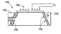
- FIG. 2a portion of a processing chamber sidewall in accordance with one embodiment of the invention is shown generally at 24 a .
- Like numerals from the above-described embodimenthave been utilized where appropriate, with differences being indicated by the suffix “a”.
- a dielectric liner 32is provided within chamber 20 and covers at least a portion of interior sidewall 24 a .
- Sidewall 24 ais preferably configured to be grounded during plasma etching operations as will become apparent below.
- dielectric liner 32comprises an anodized layer of material, formed through conventional anodization techniques.
- An exemplary dielectric materialis Al 2 O 3 .
- anodized layer 32is formed to have a thickness t of no less than about 5 mils, and is received over less than an entirety of interior sidewall 24 a .
- FIG. 3where passageways 34 are shown to expose a portion of interior sidewall 24 a .
- the passagewaysare preferably positioned to expose one or more groundable portions of sidewall 24 a .
- passageways 34provide a grounding path to the grounded sidewall portions for plasma which is generated within the chamber.
- Layer 32can be provided or formed over sidewall 24 a in any suitable way.
- layer 32is first formed over the interior sidewall to define a dielectric liner body. Thereafter, portions of the dielectric liner body are removed sufficiently to provide a plurality of passageways 34 .
- passageways 34are provided or formed to extend through and be surrounded or enclosed by material of the dielectric liner body. Accordingly, such passageways form a plurality of holes or openings received by the dielectric liner proximate the groundable portion of the interior sidewall.
- passageways or openings 34are provided such that the dielectric liner or liner body is disposed over greater than about 10% of the surface area of interior sidewall 24 a.
- grounding pathsare determined and appropriate grounding points are selected.
- Materialis then selected for the groundable portion of the interior sidewall. Selection of the material for the groundable interior sidewall portion can be tailored to reduce formation of non-volatile byproducts. In this manner, openings in the dielectric liner or cover can outwardly expose the material comprising the groundable sidewall portion(s).
- Exemplary materials of choice for the groundable sidewall portionare silicon carbide or silicon to reduce formation of undesirable byproducts. Materials can also be selected to react with the various etch chemistries to form volatile products.
- FIG. 4another processing chamber embodiment is set forth.
- a portion of a dual-source plasma etcherincludes a processing chamber 20 b .
- the illustrated etcheris the TCP 9100 high-density oxide etch system, which is available through Lam Research Corporation of Fremont, Calif.
- a portion of chamber 20 bhas been broken away to show a dielectric liner or cover 32 b which is disposed over the entirety of interior sidewall 24 b .
- Such configurationhas led to some of the above-described etch non-uniformities which are addressed and improved upon by certain aspects of the invention.
- a plurality of passageways or openings 34 bare formed or otherwise provided within dielectric liner body 32 b . Such openings are positioned to preferably expose a gas plasma developed therewithin to groundable portions of interior sidewall 24 b . Doing so has been observed to improve etch uniformity across a wafer. Such is illustrated in FIG. 10 where a portion of a gas plasma, indicated by the stippled shading, is seen to electrically contact a grounded portion of sidewall 24 b.
- dielectric liner body 32 bis removably mountable within chamber 20 b and comprises a generally frustum-shaped interior surface 36 .
- the liner bodyis preferably formed, in this example, away from chamber 20 and separately provided with passageways 34 b as shown in FIG. 7 .
- passageways 34 bcomprise a plurality of holes which extend through liner body 32 b and have a generally elongated shape in a direction generally parallel with interior surface 36 .
- Passageways or holes 34 bcan, however, have any desired shape, number, and/or orientation.
- FIGS. 8 and 9two different dielectric liner bodies, in accordance with alternate embodiments of the invention, are shown generally at 32 c and 32 d respectively. Like numerals from the above-described embodiment have been utilized where appropriate with differences being indicated by the suffixes “c” and “d”, respectively.
- Dielectric liner body 32 c(FIG. 8) is configured to be mounted over at least a bottommost portion of interior sidewall 24 b (FIG. 4 ). Accordingly, a grounding path would be provided by a passageway which is disposed over or above dielectric liner body 32 c when mounted in processing chamber 20 b (FIG. 4 ). In this example, the passageway defining the grounding path is neither surrounded by nor enclosed by dielectric liner material.
- Dielectric liner body 32 d(FIG. 9) is configured to be mounted over at least an uppermost portion of interior sidewall 24 b (FIG. 4 ). Accordingly, a grounding path would be provided by a passageway which is disposed below or under dielectric liner body 32 d when mounted in processing chamber 20 b (FIG. 4 ). In this example, the passageway defining the grounding path is neither surrounded by nor enclosed by dielectric liner material.
- FIGS. 14 and 15two alternate exemplary embodiments are shown. These embodiments can provide plasma processing tools having chambers which can be specifically engineered to achieve desired grounding paths for the plasma as described above, and which are formed from material which can be selected to reduce, or eliminate undesirable formation of non-volatile by-products.
- the various described tool embodimentscan be less expensive to build and maintain than currently available tools.
- grounding paths or pointsPreliminarily, by determining the location or locations of the grounding paths or points, one can take measures to ensure that grounding takes place through these paths or points. Materials can then be selected for the grounding surfaces which are selected to reduce formation of non-volatile by-products.
- FIGS. 14 and 15show portions of an interior groundable chamber surface at 38 , 38 a respectively.
- Surfaces 38 , 38 aare configured for grounding during operation of the processing tool of which they are a part. Each surface generally has a surface area.
- at least one grounding electrode 40 , 40 a respectivelyis disposed over and in operative contact with surface 38 , 38 a respectively. More preferably, a plurality of grounding electrodes are provided and discretely positioned over surfaces 38 , 38 a respectively.
- a grounding pathis established through one or more of the electrodes.
- the illustrated and preferred grounding electrodescover less than an entirety of the surface area of surfaces 38 , 38 a .
- each illustrated grounding electrode 40 , 40 ahas a small gap between it and a next adjacent grounding electrode. Each gap potentially leaves a portion surface 38 , 38 a , e.g. surface portions 42 , 42 a respectively, exposed.
- a dielectric covering 44 , 44 ais provided and disposed over the remaining portions of surface 38 , 38 a , i.e. portions 42 , 42 a .
- a plurality of dielectric coveringsare provided and discretely positioned over the surface area. The dielectric covering ensures that the risk of exposure of surfaces 38 , 38 a to the processing environment inside of the chamber is reduced, thereby avoiding corrosion and the like.
- one of the grounding electrode and the dielectric coveringoverlaps the other of the grounding electrode and the dielectric covering.
- portions of dielectric coverings 44overlap with their associated grounding electrodes 40 .
- the grounding electrodesare simply mounted on or over surface 38 , with dielectric coverings 44 being mounted on or over electrodes 40 .
- portions of grounding electrodes 40 aoverlap with their associated dielectric coverings.
- portions of surface 38 acan be removed to form slots within which dielectric material can be deposited.
- Exemplary materials for grounding electrodes 40 , 40 ainclude silicon carbide or silicon. Other materials can be utilized, and can be specifically selected to reduce the possibilities of undesirable reactions with chamber reactants during processing.
- One advantage provided by these embodimentsare that certain materials of choice for the grounding electrodes are much less expensive, and are more easily produced when they are produced in smaller pieces. In this way, and in some applications, a grounding electrode “mosaic” can be assembled from the individual discrete grounding electrodes.
- a grounding nodeis provided and disposed over and in operative contact with surfaces 38 , 38 a respectively. Respective plasma grounding paths can be established during operation through the grounding nodes.
- Exemplary grounding node portionsare respectively provided by electrodes 40 , 40 a in FIGS. 14 and 15.
- the illustrated grounding nodeseach have at least one, and more likely a plurality of openings over a portion of the surface area of surfaces 38 , 38 a respectively.
- Exemplary surface area portionsare shown at 42 , 42 a respectively.
- at least one dielectric covering, and more likely a plurality of dielectric coveringsare disposed over surface area portions 42 , 42 a .
- the dielectric coveringsare preferably discretely positioned over surfaces 38 , 38 a .
- a portion of at least one grounding nodeis disposed intermediate the dielectric covering and groundable surface 38 .
- a region of overlapis defined between each dielectric covering 44 and its associated intermediately-disposed grounding node portion.
- dielectric coverings 44 aare received within the interior conductive groundable surface 38 a .
- the grounding nodecomprises grounding node portions which are received over both the groundable surface 38 a and the dielectric covering 44 a.
- the percentage of surface area coverage of the dielectric coveringcan be quite small as compared with the overall surface area available, or, the surface area covered by electrodes 40 , 40 a respectively. For is example, surface area percentages as small as 0.01% can be covered by the dielectric material.
- two portions of a semiconductive wafer 100are shown generally at 102 , 104 and constitute portions of the same wafer which are spaced apart over the wafer body in accordance with the prior art.
- portion 102constitutes a portion at or near the edge of a wafer
- portion 104constitutes a portion at or near the center of the wafer.
- FIGS. 12 and 13a pair of similarly spaced-apart substrate features 106 a , 108 a , and 106 b , 108 b , respectively, are shown. Such constitute features which were etched using the above-described TCP 9100 high-density oxide etch system with a modified dielectric liner body, i.e. one that covers less than an entirety of the chamber's sidewall. Features were etched near the edge of a wafer ( 106 a , 106 b ), and near the center of the wafer ( 108 a , 108 b ). Such features are generally uniform in taper, appearance, and configuration.
- etch non-uniformitiescan be reduced, if not eliminated, thereby increasing the quality of resultant semiconductor devices.
- advantagesare gained in that internal chamber components can be protected by a dielectric liner or cover, while rendering desirable etch uniformities.
- uniformities in depositionscan also be attained utilizing the inventive plasma processing tools and methods described above. More specifically, depositions conducted under RF bias conditions can have increased uniformities.
Landscapes
- Engineering & Computer Science (AREA)
- Physics & Mathematics (AREA)
- Plasma & Fusion (AREA)
- Chemical & Material Sciences (AREA)
- Analytical Chemistry (AREA)
- General Physics & Mathematics (AREA)
- Condensed Matter Physics & Semiconductors (AREA)
- Manufacturing & Machinery (AREA)
- Computer Hardware Design (AREA)
- Microelectronics & Electronic Packaging (AREA)
- Power Engineering (AREA)
- Drying Of Semiconductors (AREA)
- Plasma Technology (AREA)
- Physical Or Chemical Processes And Apparatus (AREA)
Abstract
Description
Claims (76)
Priority Applications (1)
| Application Number | Priority Date | Filing Date | Title |
|---|---|---|---|
| US09/598,589US6184146B1 (en) | 1998-08-28 | 2000-06-20 | Plasma producing tools, dual-source plasma etchers, dual-source plasma etching methods, and method of forming planar coil dual-source plasma etchers |
Applications Claiming Priority (3)
| Application Number | Priority Date | Filing Date | Title |
|---|---|---|---|
| US09/141,810US6074953A (en) | 1998-08-28 | 1998-08-28 | Dual-source plasma etchers, dual-source plasma etching methods, and methods of forming planar coil dual-source plasma etchers |
| US09/435,237US6114252A (en) | 1998-08-28 | 1999-11-05 | Plasma processing tools, dual-source plasma etchers, dual-source plasma etching methods, and methods of forming planar coil dual-source plasma etchers |
| US09/598,589US6184146B1 (en) | 1998-08-28 | 2000-06-20 | Plasma producing tools, dual-source plasma etchers, dual-source plasma etching methods, and method of forming planar coil dual-source plasma etchers |
Related Parent Applications (1)
| Application Number | Title | Priority Date | Filing Date |
|---|---|---|---|
| US09/435,237ContinuationUS6114252A (en) | 1998-08-28 | 1999-11-05 | Plasma processing tools, dual-source plasma etchers, dual-source plasma etching methods, and methods of forming planar coil dual-source plasma etchers |
Publications (1)
| Publication Number | Publication Date |
|---|---|
| US6184146B1true US6184146B1 (en) | 2001-02-06 |
Family
ID=22497367
Family Applications (4)
| Application Number | Title | Priority Date | Filing Date |
|---|---|---|---|
| US09/141,810Expired - LifetimeUS6074953A (en) | 1998-08-28 | 1998-08-28 | Dual-source plasma etchers, dual-source plasma etching methods, and methods of forming planar coil dual-source plasma etchers |
| US09/435,237Expired - LifetimeUS6114252A (en) | 1998-08-28 | 1999-11-05 | Plasma processing tools, dual-source plasma etchers, dual-source plasma etching methods, and methods of forming planar coil dual-source plasma etchers |
| US09/515,362Expired - LifetimeUS6136720A (en) | 1998-08-28 | 2000-02-29 | Plasma processing tools dual-source plasma etchers, dual-source plasma etching methods, and methods of forming planar coil dual-source plasma etchers |
| US09/598,589Expired - LifetimeUS6184146B1 (en) | 1998-08-28 | 2000-06-20 | Plasma producing tools, dual-source plasma etchers, dual-source plasma etching methods, and method of forming planar coil dual-source plasma etchers |
Family Applications Before (3)
| Application Number | Title | Priority Date | Filing Date |
|---|---|---|---|
| US09/141,810Expired - LifetimeUS6074953A (en) | 1998-08-28 | 1998-08-28 | Dual-source plasma etchers, dual-source plasma etching methods, and methods of forming planar coil dual-source plasma etchers |
| US09/435,237Expired - LifetimeUS6114252A (en) | 1998-08-28 | 1999-11-05 | Plasma processing tools, dual-source plasma etchers, dual-source plasma etching methods, and methods of forming planar coil dual-source plasma etchers |
| US09/515,362Expired - LifetimeUS6136720A (en) | 1998-08-28 | 2000-02-29 | Plasma processing tools dual-source plasma etchers, dual-source plasma etching methods, and methods of forming planar coil dual-source plasma etchers |
Country Status (6)
| Country | Link |
|---|---|
| US (4) | US6074953A (en) |
| EP (1) | EP1108265A1 (en) |
| JP (1) | JP2002524843A (en) |
| KR (1) | KR100531164B1 (en) |
| AU (1) | AU5693199A (en) |
| WO (1) | WO2000013203A1 (en) |
Cited By (20)
| Publication number | Priority date | Publication date | Assignee | Title |
|---|---|---|---|---|
| US20020122885A1 (en)* | 2001-03-01 | 2002-09-05 | Micron Technology, Inc. | Methods, systems, and apparatus for uniform chemical-vapor depositions |
| US20030075273A1 (en)* | 2001-08-15 | 2003-04-24 | Olli Kilpela | Atomic layer deposition reactor |
| US20030207032A1 (en)* | 2002-05-02 | 2003-11-06 | Micron Technology, Inc. | Methods, systems, and apparatus for atomic-layer deposition of aluminum oxides in integrated circuits |
| US20030227033A1 (en)* | 2002-06-05 | 2003-12-11 | Micron Technology, Inc. | Atomic layer-deposited HfA1O3 films for gate dielectrics |
| US20050023594A1 (en)* | 2002-06-05 | 2005-02-03 | Micron Technology, Inc. | Pr2O3-based la-oxide gate dielectrics |
| US20050037154A1 (en)* | 2001-11-08 | 2005-02-17 | Koh Won Yong | Method for forming thin film |
| US20060244082A1 (en)* | 2005-04-28 | 2006-11-02 | Micron Technology, Inc. | Atomic layer desposition of a ruthenium layer to a lanthanide oxide dielectric layer |
| US20060276037A1 (en)* | 2001-08-06 | 2006-12-07 | Lee Chun S | Plasma enhanced atomic layer deposition (PEALD) equipment and method of forming a conducting thin film using the same thereof |
| US20070040634A1 (en)* | 2005-03-30 | 2007-02-22 | Matsushita Electric Industrial Co., Ltd. | Transmission line |
| US7405454B2 (en) | 2003-03-04 | 2008-07-29 | Micron Technology, Inc. | Electronic apparatus with deposited dielectric layers |
| US20080241387A1 (en)* | 2007-03-29 | 2008-10-02 | Asm International N.V. | Atomic layer deposition reactor |
| US20080248200A1 (en)* | 2005-06-02 | 2008-10-09 | Asm America, Inc. | Apparatus and methods for isolating chemical vapor reactions at a substrate surface |
| US20090035946A1 (en)* | 2007-07-31 | 2009-02-05 | Asm International N.V. | In situ deposition of different metal-containing films using cyclopentadienyl metal precursors |
| US20090047426A1 (en)* | 2007-08-17 | 2009-02-19 | Asm Genitech Korea Ltd. | Deposition apparatus |
| US7560793B2 (en) | 2002-05-02 | 2009-07-14 | Micron Technology, Inc. | Atomic layer deposition and conversion |
| US20090269941A1 (en)* | 2008-04-25 | 2009-10-29 | Asm America, Inc. | Plasma-enhanced deposition process for forming a metal oxide thin film and related structures |
| US7728626B2 (en) | 2002-07-08 | 2010-06-01 | Micron Technology, Inc. | Memory utilizing oxide nanolaminates |
| US20100266765A1 (en)* | 2009-04-21 | 2010-10-21 | White Carl L | Method and apparatus for growing a thin film onto a substrate |
| US7869242B2 (en) | 1999-07-30 | 2011-01-11 | Micron Technology, Inc. | Transmission lines for CMOS integrated circuits |
| US8501563B2 (en) | 2005-07-20 | 2013-08-06 | Micron Technology, Inc. | Devices with nanocrystals and methods of formation |
Families Citing this family (13)
| Publication number | Priority date | Publication date | Assignee | Title |
|---|---|---|---|---|
| US6129808A (en)* | 1998-03-31 | 2000-10-10 | Lam Research Corporation | Low contamination high density plasma etch chambers and methods for making the same |
| US6335293B1 (en) | 1998-07-13 | 2002-01-01 | Mattson Technology, Inc. | Systems and methods for two-sided etch of a semiconductor substrate |
| US20040149214A1 (en)* | 1999-06-02 | 2004-08-05 | Tokyo Electron Limited | Vacuum processing apparatus |
| US7086347B2 (en) | 2002-05-06 | 2006-08-08 | Lam Research Corporation | Apparatus and methods for minimizing arcing in a plasma processing chamber |
| US7232767B2 (en)* | 2003-04-01 | 2007-06-19 | Mattson Technology, Inc. | Slotted electrostatic shield modification for improved etch and CVD process uniformity |
| US7780791B2 (en)* | 2004-06-30 | 2010-08-24 | Lam Research Corporation | Apparatus for an optimized plasma chamber top piece |
| US8540843B2 (en) | 2004-06-30 | 2013-09-24 | Lam Research Corporation | Plasma chamber top piece assembly |
| US8141514B2 (en)* | 2006-03-23 | 2012-03-27 | Tokyo Electron Limited | Plasma processing apparatus, plasma processing method, and storage medium |
| JP4904202B2 (en)* | 2006-05-22 | 2012-03-28 | ジーイーエヌ カンパニー リミッテッド | Plasma reactor |
| KR200475462Y1 (en)* | 2009-03-27 | 2014-12-03 | 램 리써치 코포레이션 | Replaceable upper chamber section of plasma processing apparatus |
| KR200479181Y1 (en) | 2009-09-10 | 2015-12-30 | 램 리써치 코포레이션 | Replaceable upper chamber parts of plasma processing apparatus |
| TWI502617B (en) | 2010-07-21 | 2015-10-01 | 應用材料股份有限公司 | Method,plasma processing apparatus ,and liner assembly for tuning electrical skews |
| US20140225502A1 (en)* | 2013-02-08 | 2014-08-14 | Korea Institute Of Machinery & Materials | Remote plasma generation apparatus |
Citations (19)
| Publication number | Priority date | Publication date | Assignee | Title |
|---|---|---|---|---|
| US4595452A (en) | 1985-03-11 | 1986-06-17 | Oerlikon-Buhrle U.S.A. Inc. | Method and apparatus for plasma etching |
| US4948458A (en) | 1989-08-14 | 1990-08-14 | Lam Research Corporation | Method and apparatus for producing magnetically-coupled planar plasma |
| US5277751A (en) | 1992-06-18 | 1994-01-11 | Ogle John S | Method and apparatus for producing low pressure planar plasma using a coil with its axis parallel to the surface of a coupling window |
| US5304279A (en) | 1990-08-10 | 1994-04-19 | International Business Machines Corporation | Radio frequency induction/multipole plasma processing tool |
| US5366585A (en) | 1993-01-28 | 1994-11-22 | Applied Materials, Inc. | Method and apparatus for protection of conductive surfaces in a plasma processing reactor |
| US5368646A (en) | 1990-12-11 | 1994-11-29 | Lam Research Corporation | Reaction chamber design to minimize particle generation in chemical vapor deposition reactors |
| EP0641013A2 (en) | 1993-08-27 | 1995-03-01 | Applied Materials, Inc. | High density plasma CVD and etching reactor |
| US5432315A (en) | 1991-05-31 | 1995-07-11 | Hitachi, Ltd. | Plasma process apparatus including ground electrode with protection film |
| US5460707A (en)* | 1990-07-17 | 1995-10-24 | Balzers Aktiengesellschaft | Etching or coating method and a plant therefor |
| US5552124A (en) | 1994-06-22 | 1996-09-03 | Applied Materials, Inc. | Stationary focus ring for plasma reactor |
| US5589737A (en) | 1994-12-06 | 1996-12-31 | Lam Research Corporation | Plasma processor for large workpieces |
| US5605637A (en) | 1994-12-15 | 1997-02-25 | Applied Materials Inc. | Adjustable dc bias control in a plasma reactor |
| US5643394A (en) | 1994-09-16 | 1997-07-01 | Applied Materials, Inc. | Gas injection slit nozzle for a plasma process reactor |
| US5656123A (en) | 1995-06-07 | 1997-08-12 | Varian Associates, Inc. | Dual-frequency capacitively-coupled plasma reactor for materials processing |
| US5688357A (en) | 1995-02-15 | 1997-11-18 | Applied Materials, Inc. | Automatic frequency tuning of an RF power source of an inductively coupled plasma reactor |
| EP0814495A2 (en) | 1996-06-20 | 1997-12-29 | Applied Materials, Inc. | Adjusting DC bias voltage in plasma chamber |
| WO1998014980A1 (en) | 1996-09-30 | 1998-04-09 | Lam Research Corporation | Particle controlling method and plasma processing chamber |
| EP0886298A2 (en) | 1997-06-20 | 1998-12-23 | Hitachi, Ltd. | Method and apparatus of removing a sample adsorbed by static electricity from the sample stage |
| US5900064A (en) | 1997-05-01 | 1999-05-04 | Applied Materials, Inc. | Plasma process chamber |
Family Cites Families (2)
| Publication number | Priority date | Publication date | Assignee | Title |
|---|---|---|---|---|
| US5534751A (en)* | 1995-07-10 | 1996-07-09 | Lam Research Corporation | Plasma etching apparatus utilizing plasma confinement |
| JPH09120957A (en)* | 1995-08-23 | 1997-05-06 | Fujitsu Ltd | Plasma apparatus and plasma processing method |
- 1998
- 1998-08-28USUS09/141,810patent/US6074953A/ennot_activeExpired - Lifetime
- 1999
- 1999-08-26AUAU56931/99Apatent/AU5693199A/ennot_activeAbandoned
- 1999-08-26WOPCT/US1999/019497patent/WO2000013203A1/enactiveIP Right Grant
- 1999-08-26EPEP99943939Apatent/EP1108265A1/ennot_activeWithdrawn
- 1999-08-26JPJP2000568101Apatent/JP2002524843A/enactivePending
- 1999-08-26KRKR10-2001-7002685Apatent/KR100531164B1/ennot_activeExpired - Fee Related
- 1999-11-05USUS09/435,237patent/US6114252A/ennot_activeExpired - Lifetime
- 2000
- 2000-02-29USUS09/515,362patent/US6136720A/ennot_activeExpired - Lifetime
- 2000-06-20USUS09/598,589patent/US6184146B1/ennot_activeExpired - Lifetime
Patent Citations (19)
| Publication number | Priority date | Publication date | Assignee | Title |
|---|---|---|---|---|
| US4595452A (en) | 1985-03-11 | 1986-06-17 | Oerlikon-Buhrle U.S.A. Inc. | Method and apparatus for plasma etching |
| US4948458A (en) | 1989-08-14 | 1990-08-14 | Lam Research Corporation | Method and apparatus for producing magnetically-coupled planar plasma |
| US5460707A (en)* | 1990-07-17 | 1995-10-24 | Balzers Aktiengesellschaft | Etching or coating method and a plant therefor |
| US5304279A (en) | 1990-08-10 | 1994-04-19 | International Business Machines Corporation | Radio frequency induction/multipole plasma processing tool |
| US5368646A (en) | 1990-12-11 | 1994-11-29 | Lam Research Corporation | Reaction chamber design to minimize particle generation in chemical vapor deposition reactors |
| US5432315A (en) | 1991-05-31 | 1995-07-11 | Hitachi, Ltd. | Plasma process apparatus including ground electrode with protection film |
| US5277751A (en) | 1992-06-18 | 1994-01-11 | Ogle John S | Method and apparatus for producing low pressure planar plasma using a coil with its axis parallel to the surface of a coupling window |
| US5366585A (en) | 1993-01-28 | 1994-11-22 | Applied Materials, Inc. | Method and apparatus for protection of conductive surfaces in a plasma processing reactor |
| EP0641013A2 (en) | 1993-08-27 | 1995-03-01 | Applied Materials, Inc. | High density plasma CVD and etching reactor |
| US5552124A (en) | 1994-06-22 | 1996-09-03 | Applied Materials, Inc. | Stationary focus ring for plasma reactor |
| US5643394A (en) | 1994-09-16 | 1997-07-01 | Applied Materials, Inc. | Gas injection slit nozzle for a plasma process reactor |
| US5589737A (en) | 1994-12-06 | 1996-12-31 | Lam Research Corporation | Plasma processor for large workpieces |
| US5605637A (en) | 1994-12-15 | 1997-02-25 | Applied Materials Inc. | Adjustable dc bias control in a plasma reactor |
| US5688357A (en) | 1995-02-15 | 1997-11-18 | Applied Materials, Inc. | Automatic frequency tuning of an RF power source of an inductively coupled plasma reactor |
| US5656123A (en) | 1995-06-07 | 1997-08-12 | Varian Associates, Inc. | Dual-frequency capacitively-coupled plasma reactor for materials processing |
| EP0814495A2 (en) | 1996-06-20 | 1997-12-29 | Applied Materials, Inc. | Adjusting DC bias voltage in plasma chamber |
| WO1998014980A1 (en) | 1996-09-30 | 1998-04-09 | Lam Research Corporation | Particle controlling method and plasma processing chamber |
| US5900064A (en) | 1997-05-01 | 1999-05-04 | Applied Materials, Inc. | Plasma process chamber |
| EP0886298A2 (en) | 1997-06-20 | 1998-12-23 | Hitachi, Ltd. | Method and apparatus of removing a sample adsorbed by static electricity from the sample stage |
Non-Patent Citations (2)
| Title |
|---|
| No author; "Etch Products-TCP 9100 High-Density Oxide Etch System"; undated; 1 page. |
| No author; "TCP 9100 Oxide Etcher"; undated; 7 pages. |
Cited By (38)
| Publication number | Priority date | Publication date | Assignee | Title |
|---|---|---|---|---|
| US7869242B2 (en) | 1999-07-30 | 2011-01-11 | Micron Technology, Inc. | Transmission lines for CMOS integrated circuits |
| US7410668B2 (en) | 2001-03-01 | 2008-08-12 | Micron Technology, Inc. | Methods, systems, and apparatus for uniform chemical-vapor depositions |
| US6852167B2 (en) | 2001-03-01 | 2005-02-08 | Micron Technology, Inc. | Methods, systems, and apparatus for uniform chemical-vapor depositions |
| US20020122885A1 (en)* | 2001-03-01 | 2002-09-05 | Micron Technology, Inc. | Methods, systems, and apparatus for uniform chemical-vapor depositions |
| US20050087134A1 (en)* | 2001-03-01 | 2005-04-28 | Micron Technology, Inc. | Methods, systems, and apparatus for uniform chemical-vapor depositions |
| US20060276037A1 (en)* | 2001-08-06 | 2006-12-07 | Lee Chun S | Plasma enhanced atomic layer deposition (PEALD) equipment and method of forming a conducting thin film using the same thereof |
| US20030075273A1 (en)* | 2001-08-15 | 2003-04-24 | Olli Kilpela | Atomic layer deposition reactor |
| US6820570B2 (en) | 2001-08-15 | 2004-11-23 | Nobel Biocare Services Ag | Atomic layer deposition reactor |
| US20050092249A1 (en)* | 2001-08-15 | 2005-05-05 | Olli Kilpela | Atomic layer deposition reactor |
| US20050037154A1 (en)* | 2001-11-08 | 2005-02-17 | Koh Won Yong | Method for forming thin film |
| US7589029B2 (en) | 2002-05-02 | 2009-09-15 | Micron Technology, Inc. | Atomic layer deposition and conversion |
| US20060000412A1 (en)* | 2002-05-02 | 2006-01-05 | Micron Technology, Inc. | Systems and apparatus for atomic-layer deposition |
| US7560793B2 (en) | 2002-05-02 | 2009-07-14 | Micron Technology, Inc. | Atomic layer deposition and conversion |
| US20030207032A1 (en)* | 2002-05-02 | 2003-11-06 | Micron Technology, Inc. | Methods, systems, and apparatus for atomic-layer deposition of aluminum oxides in integrated circuits |
| US7160577B2 (en) | 2002-05-02 | 2007-01-09 | Micron Technology, Inc. | Methods for atomic-layer deposition of aluminum oxides in integrated circuits |
| US7670646B2 (en) | 2002-05-02 | 2010-03-02 | Micron Technology, Inc. | Methods for atomic-layer deposition |
| US7554161B2 (en) | 2002-06-05 | 2009-06-30 | Micron Technology, Inc. | HfAlO3 films for gate dielectrics |
| US7205218B2 (en) | 2002-06-05 | 2007-04-17 | Micron Technology, Inc. | Method including forming gate dielectrics having multiple lanthanide oxide layers |
| US20030227033A1 (en)* | 2002-06-05 | 2003-12-11 | Micron Technology, Inc. | Atomic layer-deposited HfA1O3 films for gate dielectrics |
| US8093638B2 (en) | 2002-06-05 | 2012-01-10 | Micron Technology, Inc. | Systems with a gate dielectric having multiple lanthanide oxide layers |
| US20050023594A1 (en)* | 2002-06-05 | 2005-02-03 | Micron Technology, Inc. | Pr2O3-based la-oxide gate dielectrics |
| US20050023624A1 (en)* | 2002-06-05 | 2005-02-03 | Micron Technology, Inc. | Atomic layer-deposited HfAlO3 films for gate dielectrics |
| US7728626B2 (en) | 2002-07-08 | 2010-06-01 | Micron Technology, Inc. | Memory utilizing oxide nanolaminates |
| US20100244122A1 (en)* | 2002-07-08 | 2010-09-30 | Leonard Forbes | Memory utilizing oxide nanolaminates |
| US8228725B2 (en) | 2002-07-08 | 2012-07-24 | Micron Technology, Inc. | Memory utilizing oxide nanolaminates |
| US7405454B2 (en) | 2003-03-04 | 2008-07-29 | Micron Technology, Inc. | Electronic apparatus with deposited dielectric layers |
| US20070040634A1 (en)* | 2005-03-30 | 2007-02-22 | Matsushita Electric Industrial Co., Ltd. | Transmission line |
| US20060244082A1 (en)* | 2005-04-28 | 2006-11-02 | Micron Technology, Inc. | Atomic layer desposition of a ruthenium layer to a lanthanide oxide dielectric layer |
| US7662729B2 (en) | 2005-04-28 | 2010-02-16 | Micron Technology, Inc. | Atomic layer deposition of a ruthenium layer to a lanthanide oxide dielectric layer |
| US20080248200A1 (en)* | 2005-06-02 | 2008-10-09 | Asm America, Inc. | Apparatus and methods for isolating chemical vapor reactions at a substrate surface |
| US8921914B2 (en) | 2005-07-20 | 2014-12-30 | Micron Technology, Inc. | Devices with nanocrystals and methods of formation |
| US8501563B2 (en) | 2005-07-20 | 2013-08-06 | Micron Technology, Inc. | Devices with nanocrystals and methods of formation |
| US20080241387A1 (en)* | 2007-03-29 | 2008-10-02 | Asm International N.V. | Atomic layer deposition reactor |
| US20090035946A1 (en)* | 2007-07-31 | 2009-02-05 | Asm International N.V. | In situ deposition of different metal-containing films using cyclopentadienyl metal precursors |
| US20090047426A1 (en)* | 2007-08-17 | 2009-02-19 | Asm Genitech Korea Ltd. | Deposition apparatus |
| US8383525B2 (en) | 2008-04-25 | 2013-02-26 | Asm America, Inc. | Plasma-enhanced deposition process for forming a metal oxide thin film and related structures |
| US20090269941A1 (en)* | 2008-04-25 | 2009-10-29 | Asm America, Inc. | Plasma-enhanced deposition process for forming a metal oxide thin film and related structures |
| US20100266765A1 (en)* | 2009-04-21 | 2010-10-21 | White Carl L | Method and apparatus for growing a thin film onto a substrate |
Also Published As
| Publication number | Publication date |
|---|---|
| AU5693199A (en) | 2000-03-21 |
| KR100531164B1 (en) | 2005-11-28 |
| KR20010074898A (en) | 2001-08-09 |
| EP1108265A1 (en) | 2001-06-20 |
| US6136720A (en) | 2000-10-24 |
| WO2000013203A1 (en) | 2000-03-09 |
| US6074953A (en) | 2000-06-13 |
| US6114252A (en) | 2000-09-05 |
| JP2002524843A (en) | 2002-08-06 |
Similar Documents
| Publication | Publication Date | Title |
|---|---|---|
| US6184146B1 (en) | Plasma producing tools, dual-source plasma etchers, dual-source plasma etching methods, and method of forming planar coil dual-source plasma etchers | |
| US8298626B2 (en) | Methods for selective pre-coating of a plasma processing chamber | |
| US6344105B1 (en) | Techniques for improving etch rate uniformity | |
| JP5731587B2 (en) | Plasma processing chamber | |
| KR20210044906A (en) | Semiconductor substrate supports with built-in RF shields | |
| JP3125696U (en) | Internal antenna for substrate processing chamber | |
| US6302057B1 (en) | Apparatus and method for electrically isolating an electrode in a PECVD process chamber | |
| US6518190B1 (en) | Plasma reactor with dry clean apparatus and method | |
| CN111354672B (en) | Electrostatic chuck and plasma processing apparatus | |
| JP2010525612A (en) | Annular baffle | |
| US20010050267A1 (en) | Method for allowing a stable power transmission into a plasma processing chamber | |
| US6531030B1 (en) | Inductively coupled plasma etching apparatus | |
| JP2000342958A (en) | Plasma device and method of manufacturing shield plate thereof | |
| KR100541195B1 (en) | Method for cleaning metal oxide film deposition chamber and deposition apparatus for performing the same | |
| US5750208A (en) | Method for plasma downstream processing | |
| TWI877214B (en) | Plasma processing apparatuses including multiple electron sources | |
| KR102693092B1 (en) | Substrate treating apparatus and method thereof | |
| US20240191353A1 (en) | Electrochemical reduction of surface metal oxides | |
| EP1269513B1 (en) | Inductively coupled plasma etching apparatus | |
| WO2024180921A1 (en) | Etching method and plasma processing apparatus | |
| JP2006024634A (en) | Plasma process equipment | |
| US7255803B2 (en) | Method of forming contact openings | |
| KR20250032358A (en) | Liner structure and apparatus for processing a substrate including the same |
Legal Events
| Date | Code | Title | Description |
|---|---|---|---|
| STCF | Information on status: patent grant | Free format text:PATENTED CASE | |
| CC | Certificate of correction | ||
| FPAY | Fee payment | Year of fee payment:4 | |
| FPAY | Fee payment | Year of fee payment:8 | |
| FPAY | Fee payment | Year of fee payment:12 | |
| AS | Assignment | Owner name:U.S. BANK NATIONAL ASSOCIATION, AS COLLATERAL AGENT, CALIFORNIA Free format text:SECURITY INTEREST;ASSIGNOR:MICRON TECHNOLOGY, INC.;REEL/FRAME:038669/0001 Effective date:20160426 Owner name:U.S. BANK NATIONAL ASSOCIATION, AS COLLATERAL AGEN Free format text:SECURITY INTEREST;ASSIGNOR:MICRON TECHNOLOGY, INC.;REEL/FRAME:038669/0001 Effective date:20160426 | |
| AS | Assignment | Owner name:MORGAN STANLEY SENIOR FUNDING, INC., AS COLLATERAL AGENT, MARYLAND Free format text:PATENT SECURITY AGREEMENT;ASSIGNOR:MICRON TECHNOLOGY, INC.;REEL/FRAME:038954/0001 Effective date:20160426 Owner name:MORGAN STANLEY SENIOR FUNDING, INC., AS COLLATERAL Free format text:PATENT SECURITY AGREEMENT;ASSIGNOR:MICRON TECHNOLOGY, INC.;REEL/FRAME:038954/0001 Effective date:20160426 | |
| AS | Assignment | Owner name:U.S. BANK NATIONAL ASSOCIATION, AS COLLATERAL AGENT, CALIFORNIA Free format text:CORRECTIVE ASSIGNMENT TO CORRECT THE REPLACE ERRONEOUSLY FILED PATENT #7358718 WITH THE CORRECT PATENT #7358178 PREVIOUSLY RECORDED ON REEL 038669 FRAME 0001. ASSIGNOR(S) HEREBY CONFIRMS THE SECURITY INTEREST;ASSIGNOR:MICRON TECHNOLOGY, INC.;REEL/FRAME:043079/0001 Effective date:20160426 Owner name:U.S. BANK NATIONAL ASSOCIATION, AS COLLATERAL AGEN Free format text:CORRECTIVE ASSIGNMENT TO CORRECT THE REPLACE ERRONEOUSLY FILED PATENT #7358718 WITH THE CORRECT PATENT #7358178 PREVIOUSLY RECORDED ON REEL 038669 FRAME 0001. ASSIGNOR(S) HEREBY CONFIRMS THE SECURITY INTEREST;ASSIGNOR:MICRON TECHNOLOGY, INC.;REEL/FRAME:043079/0001 Effective date:20160426 | |
| AS | Assignment | Owner name:JPMORGAN CHASE BANK, N.A., AS COLLATERAL AGENT, ILLINOIS Free format text:SECURITY INTEREST;ASSIGNORS:MICRON TECHNOLOGY, INC.;MICRON SEMICONDUCTOR PRODUCTS, INC.;REEL/FRAME:047540/0001 Effective date:20180703 Owner name:JPMORGAN CHASE BANK, N.A., AS COLLATERAL AGENT, IL Free format text:SECURITY INTEREST;ASSIGNORS:MICRON TECHNOLOGY, INC.;MICRON SEMICONDUCTOR PRODUCTS, INC.;REEL/FRAME:047540/0001 Effective date:20180703 | |
| AS | Assignment | Owner name:MICRON TECHNOLOGY, INC., IDAHO Free format text:RELEASE BY SECURED PARTY;ASSIGNOR:U.S. BANK NATIONAL ASSOCIATION, AS COLLATERAL AGENT;REEL/FRAME:047243/0001 Effective date:20180629 | |
| AS | Assignment | Owner name:MICRON TECHNOLOGY, INC., IDAHO Free format text:RELEASE BY SECURED PARTY;ASSIGNOR:MORGAN STANLEY SENIOR FUNDING, INC., AS COLLATERAL AGENT;REEL/FRAME:050937/0001 Effective date:20190731 | |
| AS | Assignment | Owner name:MICRON TECHNOLOGY, INC., IDAHO Free format text:RELEASE BY SECURED PARTY;ASSIGNOR:JPMORGAN CHASE BANK, N.A., AS COLLATERAL AGENT;REEL/FRAME:051028/0001 Effective date:20190731 Owner name:MICRON SEMICONDUCTOR PRODUCTS, INC., IDAHO Free format text:RELEASE BY SECURED PARTY;ASSIGNOR:JPMORGAN CHASE BANK, N.A., AS COLLATERAL AGENT;REEL/FRAME:051028/0001 Effective date:20190731 |