US6184121B1 - Chip interconnect wiring structure with low dielectric constant insulator and methods for fabricating the same - Google Patents
Chip interconnect wiring structure with low dielectric constant insulator and methods for fabricating the sameDownload PDFInfo
- Publication number
- US6184121B1 US6184121B1US09/112,919US11291998AUS6184121B1US 6184121 B1US6184121 B1US 6184121B1US 11291998 AUS11291998 AUS 11291998AUS 6184121 B1US6184121 B1US 6184121B1
- Authority
- US
- United States
- Prior art keywords
- etching
- layer
- dielectric
- wiring
- group
- Prior art date
- Legal status (The legal status is an assumption and is not a legal conclusion. Google has not performed a legal analysis and makes no representation as to the accuracy of the status listed.)
- Expired - Lifetime
Links
- 238000000034methodMethods0.000titleclaimsabstractdescription116
- 239000012212insulatorSubstances0.000titleclaimsdescription34
- 229910052751metalInorganic materials0.000claimsabstractdescription69
- 239000002184metalSubstances0.000claimsabstractdescription69
- 230000008569processEffects0.000claimsabstractdescription53
- 230000004888barrier functionEffects0.000claimsabstractdescription46
- 238000005530etchingMethods0.000claimsabstractdescription44
- 238000002161passivationMethods0.000claimsabstractdescription42
- 239000000463materialSubstances0.000claimsabstractdescription34
- 239000011248coating agentSubstances0.000claimsabstractdescription33
- 238000000576coating methodMethods0.000claimsabstractdescription33
- 238000000151depositionMethods0.000claimsabstractdescription20
- 230000007613environmental effectEffects0.000claimsabstractdescription20
- 238000000137annealingMethods0.000claimsabstractdescription11
- 239000004065semiconductorSubstances0.000claimsabstractdescription10
- 238000004377microelectronicMethods0.000claimsabstractdescription7
- 238000010030laminatingMethods0.000claimsabstractdescription4
- 238000001020plasma etchingMethods0.000claimsdescription50
- VYPSYNLAJGMNEJ-UHFFFAOYSA-NSilicium dioxideChemical compoundO=[Si]=OVYPSYNLAJGMNEJ-UHFFFAOYSA-N0.000claimsdescription27
- 239000003989dielectric materialSubstances0.000claimsdescription27
- 239000010949copperSubstances0.000claimsdescription24
- RYGMFSIKBFXOCR-UHFFFAOYSA-NCopperChemical compound[Cu]RYGMFSIKBFXOCR-UHFFFAOYSA-N0.000claimsdescription23
- 229910052802copperInorganic materials0.000claimsdescription23
- 239000004020conductorSubstances0.000claimsdescription22
- 229910052581Si3N4Inorganic materials0.000claimsdescription21
- HQVNEWCFYHHQES-UHFFFAOYSA-Nsilicon nitrideChemical compoundN12[Si]34N5[Si]62N3[Si]51N64HQVNEWCFYHHQES-UHFFFAOYSA-N0.000claimsdescription21
- 239000004642PolyimideSubstances0.000claimsdescription16
- 229920001721polyimidePolymers0.000claimsdescription16
- 238000000623plasma-assisted chemical vapour depositionMethods0.000claimsdescription15
- 238000005229chemical vapour depositionMethods0.000claimsdescription14
- 238000000059patterningMethods0.000claimsdescription14
- 229910045601alloyInorganic materials0.000claimsdescription13
- 239000000956alloySubstances0.000claimsdescription13
- 239000007789gasSubstances0.000claimsdescription12
- 229910052782aluminiumInorganic materials0.000claimsdescription11
- 229910052814silicon oxideInorganic materials0.000claimsdescription10
- 238000000608laser ablationMethods0.000claimsdescription9
- XUIMIQQOPSSXEZ-UHFFFAOYSA-NSiliconChemical compound[Si]XUIMIQQOPSSXEZ-UHFFFAOYSA-N0.000claimsdescription8
- XAGFODPZIPBFFR-UHFFFAOYSA-NaluminiumChemical compound[Al]XAGFODPZIPBFFR-UHFFFAOYSA-N0.000claimsdescription8
- 238000005498polishingMethods0.000claimsdescription8
- 239000010703siliconSubstances0.000claimsdescription8
- 229910052710siliconInorganic materials0.000claimsdescription8
- 238000003631wet chemical etchingMethods0.000claimsdescription8
- 229920000052poly(p-xylylene)Polymers0.000claimsdescription7
- 229910052721tungstenInorganic materials0.000claimsdescription7
- IJGRMHOSHXDMSA-UHFFFAOYSA-NAtomic nitrogenChemical compoundN#NIJGRMHOSHXDMSA-UHFFFAOYSA-N0.000claimsdescription6
- 239000000853adhesiveSubstances0.000claimsdescription6
- 230000001070adhesive effectEffects0.000claimsdescription6
- 238000009792diffusion processMethods0.000claimsdescription6
- 239000000203mixtureSubstances0.000claimsdescription6
- OKTJSMMVPCPJKN-UHFFFAOYSA-NCarbonChemical compound[C]OKTJSMMVPCPJKN-UHFFFAOYSA-N0.000claimsdescription5
- 229910052799carbonInorganic materials0.000claimsdescription5
- 229910052715tantalumInorganic materials0.000claimsdescription5
- 229910052804chromiumInorganic materials0.000claimsdescription4
- 239000011521glassSubstances0.000claimsdescription4
- 238000004544sputter depositionMethods0.000claimsdescription4
- 229910052719titaniumInorganic materials0.000claimsdescription4
- 238000001723curingMethods0.000claimsdescription3
- 229910052757nitrogenInorganic materials0.000claimsdescription3
- 229910000679solderInorganic materials0.000claimsdescription3
- WFKWXMTUELFFGS-UHFFFAOYSA-NtungstenChemical compound[W]WFKWXMTUELFFGS-UHFFFAOYSA-N0.000claimsdescription3
- 239000010937tungstenSubstances0.000claimsdescription3
- 238000001704evaporationMethods0.000claimsdescription2
- 230000008020evaporationEffects0.000claimsdescription2
- 238000004528spin coatingMethods0.000claimsdescription2
- UFHFLCQGNIYNRP-UHFFFAOYSA-NHydrogenChemical compound[H][H]UFHFLCQGNIYNRP-UHFFFAOYSA-N0.000claims4
- 229910052739hydrogenInorganic materials0.000claims4
- 239000001257hydrogenSubstances0.000claims4
- 238000010884ion-beam techniqueMethods0.000claims4
- 150000002739metalsChemical class0.000claims3
- 238000000992sputter etchingMethods0.000claims3
- 229910018104Ni-PInorganic materials0.000claims2
- 229910018536Ni—PInorganic materials0.000claims2
- 229910052750molybdenumInorganic materials0.000claims2
- 229910052759nickelInorganic materials0.000claims2
- 229910052758niobiumInorganic materials0.000claims2
- 150000004767nitridesChemical class0.000claims2
- 229910052698phosphorusInorganic materials0.000claims2
- UMIVXZPTRXBADB-UHFFFAOYSA-NbenzocyclobuteneChemical compoundC1=CC=C2CCC2=C1UMIVXZPTRXBADB-UHFFFAOYSA-N0.000claims1
- -1benzocydobutenePolymers0.000claims1
- 229920000592inorganic polymerPolymers0.000claims1
- 229920000620organic polymerPolymers0.000claims1
- 229910052726zirconiumInorganic materials0.000claims1
- 238000012545processingMethods0.000abstractdescription13
- 239000010410layerSubstances0.000description100
- 235000012431wafersNutrition0.000description19
- 229920000642polymerPolymers0.000description17
- 230000008021depositionEffects0.000description10
- 239000000758substrateSubstances0.000description10
- 229910018182Al—CuInorganic materials0.000description9
- QVGXLLKOCUKJST-UHFFFAOYSA-Natomic oxygenChemical compound[O]QVGXLLKOCUKJST-UHFFFAOYSA-N0.000description8
- 238000001459lithographyMethods0.000description8
- 239000001301oxygenSubstances0.000description8
- 229910052760oxygenInorganic materials0.000description8
- 239000000377silicon dioxideSubstances0.000description8
- 238000012360testing methodMethods0.000description8
- 229910000838Al alloyInorganic materials0.000description7
- 230000001934delayEffects0.000description6
- 238000004519manufacturing processMethods0.000description6
- 229910052681coesiteInorganic materials0.000description5
- 229910052906cristobaliteInorganic materials0.000description5
- 230000006870functionEffects0.000description5
- 229910052682stishoviteInorganic materials0.000description5
- 229910052905tridymiteInorganic materials0.000description5
- 230000002411adverseEffects0.000description4
- 230000009977dual effectEffects0.000description4
- 238000002474experimental methodMethods0.000description4
- 238000003475laminationMethods0.000description4
- 229920002160CelluloidPolymers0.000description3
- 229910004166TaNInorganic materials0.000description3
- 229910004200TaSiNInorganic materials0.000description3
- 229910008482TiSiNInorganic materials0.000description3
- ATJFFYVFTNAWJD-UHFFFAOYSA-NTinChemical compound[Sn]ATJFFYVFTNAWJD-UHFFFAOYSA-N0.000description3
- 239000004964aerogelSubstances0.000description3
- 230000008901benefitEffects0.000description3
- 210000001520combAnatomy0.000description3
- 238000013461designMethods0.000description3
- 238000007772electroless platingMethods0.000description3
- 229910052734heliumInorganic materials0.000description3
- 239000011810insulating materialSubstances0.000description3
- QRXWMOHMRWLFEY-UHFFFAOYSA-NisoniazideChemical compoundNNC(=O)C1=CC=NC=C1QRXWMOHMRWLFEY-UHFFFAOYSA-N0.000description3
- 230000001590oxidative effectEffects0.000description3
- 229910052718tinInorganic materials0.000description3
- XKRFYHLGVUSROY-UHFFFAOYSA-NArgonChemical compound[Ar]XKRFYHLGVUSROY-UHFFFAOYSA-N0.000description2
- 229910017758Cu-SiInorganic materials0.000description2
- 229910017931Cu—SiInorganic materials0.000description2
- 208000033999Device damageDiseases0.000description2
- 229910001111Fine metalInorganic materials0.000description2
- XPDWGBQVDMORPB-UHFFFAOYSA-NFluoroformChemical compoundFC(F)FXPDWGBQVDMORPB-UHFFFAOYSA-N0.000description2
- 238000013459approachMethods0.000description2
- 229910052786argonInorganic materials0.000description2
- 230000015556catabolic processEffects0.000description2
- 238000004891communicationMethods0.000description2
- 238000006731degradation reactionMethods0.000description2
- 230000001419dependent effectEffects0.000description2
- 238000005137deposition processMethods0.000description2
- 230000000694effectsEffects0.000description2
- 238000009713electroplatingMethods0.000description2
- 238000005516engineering processMethods0.000description2
- 238000011049fillingMethods0.000description2
- NBVXSUQYWXRMNV-UHFFFAOYSA-NfluoromethaneChemical compoundFCNBVXSUQYWXRMNV-UHFFFAOYSA-N0.000description2
- 239000001307heliumSubstances0.000description2
- SWQJXJOGLNCZEY-UHFFFAOYSA-Nhelium atomChemical compound[He]SWQJXJOGLNCZEY-UHFFFAOYSA-N0.000description2
- 229910010272inorganic materialInorganic materials0.000description2
- 239000011147inorganic materialSubstances0.000description2
- 230000003993interactionEffects0.000description2
- 238000005240physical vapour depositionMethods0.000description2
- 238000007747platingMethods0.000description2
- 230000009291secondary effectEffects0.000description2
- 235000012239silicon dioxideNutrition0.000description2
- 239000007787solidSubstances0.000description2
- 238000012876topographyMethods0.000description2
- 206010067484Adverse reactionDiseases0.000description1
- 229910000881Cu alloyInorganic materials0.000description1
- YCKRFDGAMUMZLT-UHFFFAOYSA-NFluorine atomChemical compound[F]YCKRFDGAMUMZLT-UHFFFAOYSA-N0.000description1
- BLRPTPMANUNPDV-UHFFFAOYSA-NSilaneChemical compound[SiH4]BLRPTPMANUNPDV-UHFFFAOYSA-N0.000description1
- 238000010521absorption reactionMethods0.000description1
- 230000006838adverse reactionEffects0.000description1
- WYTGDNHDOZPMIW-RCBQFDQVSA-NalstonineNatural productsC1=CC2=C3C=CC=CC3=NC2=C2N1C[C@H]1[C@H](C)OC=C(C(=O)OC)[C@H]1C2WYTGDNHDOZPMIW-RCBQFDQVSA-N0.000description1
- 238000006243chemical reactionMethods0.000description1
- 230000007797corrosionEffects0.000description1
- 238000005260corrosionMethods0.000description1
- 230000007547defectEffects0.000description1
- 239000002355dual-layerSubstances0.000description1
- 238000003682fluorination reactionMethods0.000description1
- 229910052731fluorineInorganic materials0.000description1
- 239000011737fluorineSubstances0.000description1
- 239000006260foamSubstances0.000description1
- 230000009477glass transitionEffects0.000description1
- 238000007654immersionMethods0.000description1
- 230000006872improvementEffects0.000description1
- 150000002500ionsChemical class0.000description1
- 238000001465metallisationMethods0.000description1
- 238000005272metallurgyMethods0.000description1
- 230000005012migrationEffects0.000description1
- 238000013508migrationMethods0.000description1
- 238000012986modificationMethods0.000description1
- 230000004048modificationEffects0.000description1
- 239000002105nanoparticleSubstances0.000description1
- 230000035515penetrationEffects0.000description1
- 238000000206photolithographyMethods0.000description1
- 239000002574poisonSubstances0.000description1
- 231100000614poisonToxicity0.000description1
- 238000007517polishing processMethods0.000description1
- 229920003209poly(hydridosilsesquioxane)Polymers0.000description1
- 229920006254polymer filmPolymers0.000description1
- 239000002861polymer materialSubstances0.000description1
- 239000002243precursorSubstances0.000description1
- 230000009467reductionEffects0.000description1
- 238000001878scanning electron micrographMethods0.000description1
- 229910000077silaneInorganic materials0.000description1
- 238000005245sinteringMethods0.000description1
- 239000011343solid materialSubstances0.000description1
- 239000002904solventSubstances0.000description1
- 239000000126substanceSubstances0.000description1
- 238000011282treatmentMethods0.000description1
Images


Classifications
- H—ELECTRICITY
- H01—ELECTRIC ELEMENTS
- H01L—SEMICONDUCTOR DEVICES NOT COVERED BY CLASS H10
- H01L23/00—Details of semiconductor or other solid state devices
- H01L23/52—Arrangements for conducting electric current within the device in operation from one component to another, i.e. interconnections, e.g. wires, lead frames
- H01L23/522—Arrangements for conducting electric current within the device in operation from one component to another, i.e. interconnections, e.g. wires, lead frames including external interconnections consisting of a multilayer structure of conductive and insulating layers inseparably formed on the semiconductor body
- H01L23/532—Arrangements for conducting electric current within the device in operation from one component to another, i.e. interconnections, e.g. wires, lead frames including external interconnections consisting of a multilayer structure of conductive and insulating layers inseparably formed on the semiconductor body characterised by the materials
- H01L23/53204—Conductive materials
- H01L23/53209—Conductive materials based on metals, e.g. alloys, metal silicides
- H01L23/53228—Conductive materials based on metals, e.g. alloys, metal silicides the principal metal being copper
- H—ELECTRICITY
- H01—ELECTRIC ELEMENTS
- H01L—SEMICONDUCTOR DEVICES NOT COVERED BY CLASS H10
- H01L21/00—Processes or apparatus adapted for the manufacture or treatment of semiconductor or solid state devices or of parts thereof
- H01L21/70—Manufacture or treatment of devices consisting of a plurality of solid state components formed in or on a common substrate or of parts thereof; Manufacture of integrated circuit devices or of parts thereof
- H01L21/71—Manufacture of specific parts of devices defined in group H01L21/70
- H01L21/768—Applying interconnections to be used for carrying current between separate components within a device comprising conductors and dielectrics
- H01L21/76801—Applying interconnections to be used for carrying current between separate components within a device comprising conductors and dielectrics characterised by the formation and the after-treatment of the dielectrics, e.g. smoothing
- H01L21/7682—Applying interconnections to be used for carrying current between separate components within a device comprising conductors and dielectrics characterised by the formation and the after-treatment of the dielectrics, e.g. smoothing the dielectric comprising air gaps
- H—ELECTRICITY
- H01—ELECTRIC ELEMENTS
- H01L—SEMICONDUCTOR DEVICES NOT COVERED BY CLASS H10
- H01L23/00—Details of semiconductor or other solid state devices
- H01L23/52—Arrangements for conducting electric current within the device in operation from one component to another, i.e. interconnections, e.g. wires, lead frames
- H01L23/522—Arrangements for conducting electric current within the device in operation from one component to another, i.e. interconnections, e.g. wires, lead frames including external interconnections consisting of a multilayer structure of conductive and insulating layers inseparably formed on the semiconductor body
- H01L23/5222—Capacitive arrangements or effects of, or between wiring layers
- H—ELECTRICITY
- H01—ELECTRIC ELEMENTS
- H01L—SEMICONDUCTOR DEVICES NOT COVERED BY CLASS H10
- H01L23/00—Details of semiconductor or other solid state devices
- H01L23/52—Arrangements for conducting electric current within the device in operation from one component to another, i.e. interconnections, e.g. wires, lead frames
- H01L23/522—Arrangements for conducting electric current within the device in operation from one component to another, i.e. interconnections, e.g. wires, lead frames including external interconnections consisting of a multilayer structure of conductive and insulating layers inseparably formed on the semiconductor body
- H01L23/532—Arrangements for conducting electric current within the device in operation from one component to another, i.e. interconnections, e.g. wires, lead frames including external interconnections consisting of a multilayer structure of conductive and insulating layers inseparably formed on the semiconductor body characterised by the materials
- H01L23/53204—Conductive materials
- H01L23/53209—Conductive materials based on metals, e.g. alloys, metal silicides
- H01L23/53214—Conductive materials based on metals, e.g. alloys, metal silicides the principal metal being aluminium
- H01L23/53223—Additional layers associated with aluminium layers, e.g. adhesion, barrier, cladding layers
- H—ELECTRICITY
- H01—ELECTRIC ELEMENTS
- H01L—SEMICONDUCTOR DEVICES NOT COVERED BY CLASS H10
- H01L23/00—Details of semiconductor or other solid state devices
- H01L23/52—Arrangements for conducting electric current within the device in operation from one component to another, i.e. interconnections, e.g. wires, lead frames
- H01L23/522—Arrangements for conducting electric current within the device in operation from one component to another, i.e. interconnections, e.g. wires, lead frames including external interconnections consisting of a multilayer structure of conductive and insulating layers inseparably formed on the semiconductor body
- H01L23/532—Arrangements for conducting electric current within the device in operation from one component to another, i.e. interconnections, e.g. wires, lead frames including external interconnections consisting of a multilayer structure of conductive and insulating layers inseparably formed on the semiconductor body characterised by the materials
- H01L23/53204—Conductive materials
- H01L23/53209—Conductive materials based on metals, e.g. alloys, metal silicides
- H01L23/53228—Conductive materials based on metals, e.g. alloys, metal silicides the principal metal being copper
- H01L23/53238—Additional layers associated with copper layers, e.g. adhesion, barrier, cladding layers
- H—ELECTRICITY
- H01—ELECTRIC ELEMENTS
- H01L—SEMICONDUCTOR DEVICES NOT COVERED BY CLASS H10
- H01L23/00—Details of semiconductor or other solid state devices
- H01L23/52—Arrangements for conducting electric current within the device in operation from one component to another, i.e. interconnections, e.g. wires, lead frames
- H01L23/522—Arrangements for conducting electric current within the device in operation from one component to another, i.e. interconnections, e.g. wires, lead frames including external interconnections consisting of a multilayer structure of conductive and insulating layers inseparably formed on the semiconductor body
- H01L23/532—Arrangements for conducting electric current within the device in operation from one component to another, i.e. interconnections, e.g. wires, lead frames including external interconnections consisting of a multilayer structure of conductive and insulating layers inseparably formed on the semiconductor body characterised by the materials
- H01L23/5329—Insulating materials
- H—ELECTRICITY
- H01—ELECTRIC ELEMENTS
- H01L—SEMICONDUCTOR DEVICES NOT COVERED BY CLASS H10
- H01L2924/00—Indexing scheme for arrangements or methods for connecting or disconnecting semiconductor or solid-state bodies as covered by H01L24/00
- H01L2924/0001—Technical content checked by a classifier
- H01L2924/0002—Not covered by any one of groups H01L24/00, H01L24/00 and H01L2224/00
Definitions
- This inventionpertains to the field of microelectronic chip fabrication for logic, memory, communication and microcontroller applications.
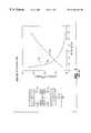
- the capacitance of a signal lineis a combination of the mutual capacitance between the lines in the same wiring plane (C LL ) and between lines in two different levels (C CO or C LG ) as shown in FIG. 1, cited from a recent conference (R. Havemann presented at the Proceedings of the 1996 Symposium on VLSI Technology, Honolulu, Hi., Jun. 10, 1996).
- C LLthe same wiring plane
- C CO or C LGthe two different levels
- a whole gamut of insulator materials including fluorinated silica, polymers with and without fluorination, amorphous teflon-like polymers, and aerogels made of porous silicahave been proposed as possible low K materials for this purpose.
- FIGS. 2A to 2 D and later in FIGS. 4A to 4 Dwe depict the wafer at this stage of processing as the semiconductor substrate, 10 , in FIGS. 2A to 2 D and later in FIGS. 4A to 4 D.
- Two layers of dielectrics, 20 and 30are applied on said semiconductor substrate and patterned by lithography and plasma etching to produce trenches, 50 , on the top layer that represent the wiring tracks and vias, 40 , in the lower layer that will become the means to connect the wires to the metal level below, as shown in FIG. 2 A.
- Layers 20 and 30can be made of the same dielectric in which case they can be applied in a single deposition step.
- an electrically conductive barrier/adhesion layer, 60 , and a copper-based conductor layer, 70are deposited on the patterned dielectric structure by one or more of the techniques such as sputtering and/or chemical vapor deposition and electrolytic or electroless plating.
- This layerhas to be thick enough to overfill the vias, 40 , and trenches, 50 , as shown in FIG. 2 B.
- the last stepis to planarize the top surface by chemical-mechanical polishing (CMP) so that the excess copper and the barrier layer are polished off from the top surface resulting in the inlaid wire/via stack as shown in FIG. 2 C.
- CMPchemical-mechanical polishing
- This sequenceis repeated several times till the necessary number of wiring layers are built.
- the waferis coated with an insulating passivation layer, 80 , and terminal metal pads, 90 , are deposited and connected to the top most wiring level through suitable vias in the passivation layer, 80 , as shown in FIG. 2 D. These terminal pads are used to assemble the chip on a chip carrier using solder interconnects which enables the chip to communicate with other chips and to send and receive information to the user.
- Alternate terminal pad processes and structurescan also be used in place of the final step described above which enable interconnection using wire bonding, conductive paste bonding and the like.
- the wafersare subjected to a 400° C. anneal in a N 2 /H 2 mixture to “anneal out” any damage accumulated in the thin gate oxide under the silicon circuit gates due to the various plasma processes used to fabricate the wiring structure.
- the adhesion/barrier layer described abovehas to function as a copper diffusion barrier.
- the adhesion/barrier layerhas to be free of defects and rapid diffusion paths such as grain boundaries.
- conductive barrier films of sizable film thicknessSince the typical conductive barrier films have high electrical resistivity, the presence of a significant thickness of such a film in the conductor cross section leads to an increase in the effective line resistance of the wiring. This is particularly severe for narrow lines typical of advanced chips, where the barrier thickness becomes a significant fraction of the line width itself.
- Low K dielectricsare also not compatible with Al—Cu interconnect processing because 400° C. to 450° C. substrate temperatures during deposition and/or post deposition anneals are still required to achieve reliable microstructure and properties of the Al—Cu lines, and repeated excursions to such temperatures (in addition to the final device damage anneal) tend to lead to degradation of many of the low K polymeric insulators, as mentioned earlier.
- the level of conformality versus planarity of the CVD polymer coatingis dependent on the feature size and spacing and hence will be pattern dependent within the same wafer. This makes it difficult to ensure definitively what the exact nature of the dielectric medium would be around any given line in an interconnect design. This makes the task of predicting and accounting for interconnect delays in chip designs very difficult.
- the processis tailored to work with the subtractively patterned Al-based wiring structures and may not be suitable for the dual damascene process (Al or Cu based) since the dielectric layers with trenches or vias are made first and metal is filled in and planarized with the patterned dielectric stack in a subsequent step. This precludes the use of the processing route described in FIG. 3, proposed by Jeng et al., for interconnect structures fabricated by the damascene process.
- the second method taught by Chang et al., U.S. Pat. No. 5,559,055,describes a process in which one layer of aluminum-based interconnect wiring, the insulator (silicon dioxide) and a stud layer deposited into the vias in the insulator are first fabricated. A second interconnect wiring layer of Al alloy is then deposited and patterned on top. At this point, the insulator is removed either completely or only from between the metal features by an etching process. The structure is then either fully or partially filled with a lower dielectric constant material. A passivation layer is then deposited over the resulting structure. A net lowering of the dielectric constant is claimed due to the replacement of the oxide material with a lower K insulator with or without trapped voids filled with air.
- Chang et al.teach a method that is restricted to wiring structures based on subtractively etched metal lines (aluminum based) only and do not teach a method to achieve lower effective K in structures made by a damascene process, as described in FIG. 2 .
- a low K dielectricpreferably air
- a broad aspect of the present inventionis a low dielectric constant chip interconnect wiring structure and a method to fabricate said structure, including the steps of:
- an integrated circuit (IC) interconnect wiring structurecontaining one or more wiring and via levels using an aluminum or copper-based conductor material and a suitable organic or inorganic insulator material by using methods well known in the current state of the art such as sputter deposition, plating, chemical vapor deposition (CVD), plasma enhanced CVD (PECVD), and reactive ion etching (RIE) combined with lithographic patterning and chemical-mechanical polishing (CMP);
- CVDchemical vapor deposition
- PECVDplasma enhanced CVD
- RIEreactive ion etching
- etching processsuch as reactive ion etching, wet chemical etching, electron cyclotron resonance (ECR) down stream etching or laser ablative etching;
- the dielectric etch and cover layer attachmentare carried out only for the upper most pair of wiring levels while retaining the lower levels of wiring as is with the original high K dielectric in order to simplify the overall process.
- FIG. 1is a schematic cross section of a multilevel chip interconnect structure showing the different capacitive components that contribute to signal delay, with a data plot showing the relationship between feature size and intralevel capacitance C LL , inter level capacitance C LG and the total capacitance C T .
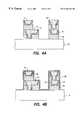
- FIG. 2Ashows the cross section of the dual layer dielectric structure with etched vias and trenches for wiring tracks during the fabrication of a multilevel interconnect wiring stack.
- FIG. 2Bshows the cross section of the structure from FIG. 2A after it has been overfilled with barrier and conducting metal layers.
- FIG. 2Cshows the cross section of the structure from FIG. 2B after it has been planarized by chemical-mechanical polishing.
- FIG. 2Dshows the cross section of the finished multilayer stack with its I/O terminal pads.
- FIG. 3is a schematic sketch of the prior art process to achieve embedded low K dielectric structures.
- FIG. 4Ais a schematic sketch of an interconnect structure produced by damascene polishing process followed by dielectric etch to remove all the dielectric material that is not covered by metal features.
- FIG. 4Bis a schematic sketch of the structure shown in FIG. 4A after a high temperature forming gas anneal and the deposition of a conformed thin passivation dielectric layer.
- FIG. 4Cis the schematic sketch of the structure shown in FIG. 4B after laminating a free standing insulating cover layer and applying a thin environmental barrier layer.
- FIG. 4Dis the schematic sketch of the structure shown in FIG. 4C after terminal vias have been etched and terminal pads are deposited to complete the fabrication of the structure.
- FIG. 5is a scanning electron microscope (SEM) photo of an actual three level trace-via-trace test structure with copper wiring made by the damascene process, said test structure having been plasma etched to remove the polymer dielectric film from between the metal features in the same wiring plane.
- SEMscanning electron microscope
- FIG. 6is an SEM photograph of a three level test structure with Al—Cu alloy wiring and oxide dielectric fabricated by a subtractive process, after etching the dielectric material from between the features in the same wiring plane.
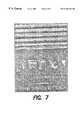
- FIG. 7is an SEM cross sectional photograph of a three level structure that has been plasma etched to remove the dielectric between the features in the same level and then coated with a thin conformal silicon nitride passivation layer to protect the metal features.
- a low dielectric constant multilevel wiring structureis created by the following damascene-type sequence:
- a layer of an insulating ionic barrier such as silicon nitride, PSG or BPSGis applied over these devices and appropriate contact vias are opened in this layer by lithography and RIE.
- Such a waferis schematically designated as the semiconductor substrate, 10 , in FIGS. 2A through 2D and subsequently in FIGS. 4A through 4D that are used in the following description.
- an insulating materialsuch as polyimide Pyralin 2611 or Polyimide 5878 (manufactured by Dupont Inc.) is applied and cured on the semiconductor substrate resulting in layers 20 and 30 , to achieve a total thickness required for two interconnect metal levels.
- an inorganic dielectricsuch as silicon dioxide, silicon nitride or spin-on-glass films can also be used to fabricate these layers.
- the insulator material making up layers 20 and 30is chosen for its processability, low internal stress, CMP compatibility and ease of etching by RIE with good selectivity with respect to the metal.
- Trenches and via holes where the wiring traces are to be locatedare then formed in the dielectric stack by lithography and RIE.
- An electrically conductive adhesion/barrier layer(such as Cr, Ta, Ti, W, TiN, TaN, WN, TiSiN or TaSiN or combinations thereof) is applied.
- the trenches and viaare then overfilled with copper deposited by a process such as CVD, sputtering, electroplating, electroless plating, evaporation or combinations thereof.
- the structureis then planarized by chemical-mechanical polishing (CMP) such that the copper surface is coplanar with the dielectric surface resulting in a dual level metal (DLM) comprising a wiring trace/stud structure in-laid in the dielectric.
- CMPchemical-mechanical polishing
- DLMdual level metal
- An optional insulating passivation layercan be applied at this point in order to prevent any reaction between the metal conductor and the next polymer based DLM layer. Additional DLM's are added by the repetition of these process steps as required to complete all levels except the terminal vias and pads that form the upper most patterned level of the wafer.
- the waferis then placed in a plasma etch or a reactive ion etch (RIE) system and etched with a suitable gas mixture, such as one containing freon and oxygen, optimized to remove the polymer from all the areas that are not covered over by metal features with minimal etching of the metal conductor.
- RIEreactive ion etch
- a suitable gas mixturesuch as one containing freon and oxygen
- etchingsuch as wet chemical etching, laser ablation, and plasma etching can also be used to remove the dielectric material from between the metal features.
- the structureis annealed at an elevated temperature such as 400° C. for a suitable duration to reduce any plasma induced damage in the structure.
- this anneal stepcan be performed before or after the application of that passivation coating.
- a very thin dielectric passivation layer, 100such as silicon nitride, is deposited as a thin conformal coating as shown in FIG. 4 B.
- the passivation layercovers over all the exposed surfaces and is generally deposited by a PECVD process.
- This coatingwhich can be as thin as 5 to 40 nm, will act to seal and passivate all the exposed areas of the lines, vias and dielectric layers and suppress any diffusion or interaction of the metal wiring with the rest of the microelectronics component. This is particularly important since copper can poison silicon devices and adversely affect their transistor characteristics and since absorption of moisture can degrade organic dielectric performance.
- the passivation coatingcan be a CVD polymer coating such as Parylene that conformally coats the surfaces.
- a CVD polymer coatingsuch as Parylene that conformally coats the surfaces.
- another passivation optionis to use an electroless or immersion plating of a suitable barrier metal that selectively coats only the exposed metallic feature surfaces of the etched wiring structure.
- a thin free standing sheet of insulating material with an adhesive coating on one surfaceis laminated to the top of the structure to form a taut cover layer, 120 , as shown in FIG. 4 C.
- This cover layercan be an insulator with an adhesive coating on one side to allow lamination to the structure and could be made of a material such as polyimide or a photo imageable dielectric.
- the lamination processis performed preferably in an inert, non-oxidizing environment such as helium, argon or forming gas.
- An optional environmental barrier layer, 130such as silicon oxide, silicon nitride or diamond-like carbon can be deposited on top of the cover layer, 120 .
- layer 130The function of layer 130 is to prevent ingress of oxygen, moisture and other reactive species that may adversely affect the reliability of the devices and the interconnects. This results in a structure wherein the intralevel dielectric (between the metal features in a given a wiring layer) is air with a K of 1. Vias are then etched into the cover layer, 120 , the environmental barrier layer, 130 , and the thin passivation coating, 100 , at locations where contacts to the input/output terminal pads are required.
- contact metallurgy for the terminal I/O pads, 90are deposited and patterned at the proper locations and the wafer fabrication is completed.
- FIG. 4Dschematically depicts the completed low dielectric constant structure produced by the above method.
- a low dielectric constant multilevel wiring structureis created by the following sequence:
- a layer of insulating ionic barrier such as silicon nitride, PSG or BPSGis applied over these devices and appropriate contact vias are opened in this layer by lithography and RIE.
- a series of blanket films starting with a thin (less than 100 nm thick) adhesion/barrier layer material such as Cr, Ti—W, Ta, TaN, Ti, TiN, W, WN or TiSiN or TaSiN, a 500 to 1000 nm thick layer of Al—Cu or Al—Cu—Si alloy conductor material followed by a thin top layer of the same adhesion/barrier layer material as aboveare deposited in a single sequence.
- the stack of filmsis lithographically patterned into a wiring level using suitable RIE processes known in the state of the art.
- an insulator materialis coated over the metal features by CVD, PECVD or spin coating and curing processes.
- the criteria for choosing this insulatorare ease of deposition, ease of filling gaps, planarization over feature topography, low stress, ability to withstand any thermal processing needed during structure build and plasma damage annealing (essentially high thermal stability and high glass transition temperature), absence of adverse reactions with the interconnect metal stack and ease of etching with high selectivity relative to the metal stack.
- Low dielectric constantis not a key requirement for the insulator since it will serve only as the interlevel rather than the intralevel dielectric in the final structure and, hence, has only a secondary effect on the overall interconnect capacitance and delays.
- the coatingis intended to be thick enough to cover all the metallic features and produce a buffer thickness of insulator over the features so that it can be used as the next level insulator.
- Polymeric materialssuch as polyimides or inorganic materials such as SiO 2 are ideal candidates for this purpose.
- the inorganic materialsmay be more preferable due to their superior thermal stability.
- An optional planarizing materialcan be applied and reflowed as needed to achieve a planar topography if not already achieved. Spin on glasses and flowable oxides are typical examples of these planarizing materials which are compatible with the inorganic insulators. Such materials are applied at a minimum thickness required to achieve planarization.
- contact via holesare produced at appropriate locations in the insulator overcoat by lithography and RIE to expose metal regions that need to be connected to the next upper level.
- Another stack of adhesion layer, Al alloy conductor and overcoat metalare deposited on top of this structure.
- a sintering processis performed at a temperature close to or above 400° C. to reflow the Al alloy layers and to ensure good contact between the two sets of metal stacks deposited separately and to improve the microstructure of the Al alloy film itself.
- the metal blanketis then etched back by RIE or polished back to be coplanar with the insulator surface.
- the viascan be filled by a selective chemical vapor deposition process that applies a metal such as tungsten to fill the via holes only.
- the waferis subjected to reactive ion etching in a plasma comprising, for example, a fluorine containing gas (such as CF 4 or SF 6 , for example) and oxygen to etch the dielectric materials not covered by the aluminum alloy lines.
- a fluorine containing gassuch as CF 4 or SF 6 , for example
- oxygento etch the dielectric materials not covered by the aluminum alloy lines.
- Other methodssuch as wet chemical etching or laser ablation etching can also be employed to accomplish this result.
- the resulting structureis subjected to any elevated temperature (greater than 400° C.) annealing treatments required to remove plasma damage to the underlying IC devices.
- this anneal stepcan be performed before or after the application of that passivation coating.
- an optional dielectric passivation layersuch as silicon nitride is deposited as a thin conformal coating over all the exposed surfaces by a process such as, but not limited to, PECVD.
- This coatingwhich can be as thin as 30 to 40 nm will act to seal the side walls of all the lines and vias and suppress the degradation of the wiring metal and the dielectric during subsequent processing.
- the passivation coatingcan be a CVD polymer coating such as Parylene that conformally coats the surfaces.
- a thin free standing sheet of an insulator with an adhesive coating on one surfaceis laminated to the top of the structure to form a taut cover layer.
- This laminationis preferably performed in a He, Ar, forming gas or a similar non-oxidizing ambient.
- An optional environmental barrier layersuch as silicon oxide, silicon nitride or diamond-like carbon can be deposited on top of the cover layer.
- the function of layeris to prevent ingress of oxygen, moisture and other reactive species that may adversely affect the reliability of the devices and the interconnects. This results in a structure wherein the intralevel dielectric (between the metal features in a given a wiring layer) is air with a K of 1. Vias are then etched into the cover layer, the environmental barrier layer and the thin passivation coating at locations where contacts to the input/output terminal pads are required.
- terminal metal padsare deposited at the above noted via locations to complete the device structure.
- the aluminum alloy wiringcan be fabricated by a damascene-type process to achieve the initial multilevel structure.
- the following procedureis used to fabricate the low K dielectric-containing final structure:
- a layer of ionic barriersuch as silicon nitride, PSG or BPSG is applied over these devices and appropriate contact vias are opened in this layer by lithography and RIE.
- a layer of insulating materialsuch as polyimide Pyralin 2611 by Dupont Inc. is spin coated and cured to achieve a total thickness required for two metal/dielectric interconnect levels.
- the polymeris chosen for its processability, low internal stress upon curing, CMP compatibility and ease of etching by RIE.
- an inorganic dielectricsuch as SiO 2 deposited by PECVD can also be used since it allows thermal processing to higher temperatures and is more amenable to CMP processing. Low K is not a requirement since this material will only be employed as an interlevel rather than an intralevel dielectric.
- the trenches where the wiring traces are to be located and via holesare produced in the dielectric stack by lithography and RIE using state of the art processes (for example, CF 4 /oxygen plasma).
- An adhesion layer metal(such as Ta, Ti, TiN, TaN, TiSiN, W, WN or TaSiN or a combination thereof) is deposited by PECVD, CVD or physical vapor deposition (PVD). This is followed by the deposition of an Al—Cu or Al—Cu—Si alloy needed to overfill the trench/via combination.
- the structureis then planarized by chemical-mechanical polishing (CMP) such that the metallic surface is coplanar with the dielectric surface resulting in a dual level metal (DLM) wiring/stud structure in-laid in the dielectric.
- CMPchemical-mechanical polishing
- a passivation layermay be applied at this point if subsequent application of insulator is required for further DLM fabrication on top. Additional DLM's are added by the repetition of these process steps as required to complete all levels except the terminal vias and pads that represent the upper most patterned level of the wafer.
- the waferis then etched in a RIE or plasma etch process optimized to etch the dielectric with minimal etching of the metal features to etch back and remove the insulator from all the areas that are not covered over by metal features.
- the metal lines and viasact as masks and the polymer in the openings between them will be etched away.
- the structureis robust since the insulator underpins all the fine metal features and holds them in place. It is annealed at an elevated temperature such as 400° C. for a suitable duration to reduce any plasma induced damage in the structure. Depending on the thermal stability and deposition process of the thin passivation layer described in the next paragraph, this anneal step can be performed before or after the application of that passivation coating.
- a dielectric passivation layersuch as silicon nitride is deposited as a thin conformal coating over all the exposed surfaces by a process such as PECVD.
- CVD polymer filmssuch as Parylene can also be used for this purpose.
- a metallic passivation/barrier layerthat can be deposited by electroless plating or selective CVD to cover only the exposed Al feature surfaces only can also be applied at this stage.
- the function of this thin passivation/barrier coatingwhich can be as thin as 30 to 40 nm is to seal and protect all exposed areas of the lines and vias and the dielectric layers and suppress any diffusion or interaction of the wiring material with the rest of the device structure.
- a thin free standing sheet of an insulator with an adhesive coating on one surfaceis laminated, preferably in a non-oxidizing ambient, to the top of the structure to form a taut cover layer.
- An optional environmental barrier layersuch as silicon oxide, silicon nitride or diamond-like carbon can be deposited on top of the cover layer. The function of this layer is to prevent ingress of oxygen, moisture and other reactive species that may adversely affect the reliability of the devices and the interconnects. This results in a structure wherein the intralevel dielectric (between the metal features in a given wiring layer) is air with a K of 1. Vias are then etched into the environmental barrier layer, the cover layer and the thin passivation coating at locations where contacts to the input/output terminal pads are required.
- terminal metal padsare deposited at the above noted via locations to complete the device structure.
- the etching of the insulator and the lamination of the cap layer and the environmental barrier layer as described in the three embodiments aboveare employed only in the top most plane pair of wiring/stud levels.
- the benefits in this caseare reduced processing cost and potential for higher yield.
- the performance benefits of the low K materialcan be harnessed by designing the interconnect layout taking into account the fact that low K air insulator and the attendant capacitance reduction are available at the upper most wiring levels.
- the intralevel dielectric in the lower wiring levelsis predominantly a solid dielectric, by which we mean that is a homogenous solid or a solid material with uniformly distributed micro or nano-sized porosity, such as polymer foams, aerogels or xerogels.
- the etch back approach proposed in the present inventionwas demonstrated by an experiment using a test wiring structure.
- This structurecomprised an oxidized silicon substrate with a first wiring layer of copper, a second via level of copper and a third wiring level of copper connected to the first level at selected locations by means of said second copper vias.
- the insulator separating the different levelswas Dupont Pyralin 2611 polyimide about 1.2 ⁇ m thick.
- the line widths of the metal featuresranged in size from 1 to 4 ⁇ m, with spacings ranging from 0.65 to 3.75 ⁇ m, and the metal thickness was about 1.2 ⁇ m.
- This structurewas subjected to RIE to remove the dielectric layers from between the metal features.
- Typical RIE conditions employed for the polyimide removalwere 10 to 30 mTorr of a CF 4 /O 2 gas mixture with 80 to 95% oxygen, at an rf power density of 0.25 to 1 Watt/cm 2 .
- the oxide RIEwas carried out in a pure CF 4 gas under similar conditions.
- FIG. 5An SEM photograph of the structure after dielectric etching is shown in FIG. 5 . It is clear that all the polymer and the oxide layers between both the closely spaced and widely spaced features have been fully removed.
- An oxidized silicon wafer with two wiring levels interconnected at selected location by a via levelwas the starting point for this experiment.
- the structureconsisted of Al—Cu alloy wiring and via studs and Ti-based or Ta-based adhesion and cap layers approximately 100 nm thick.
- the dielectric usedwas PECVD SiO 2 and the build process used to make these substrates was one where the metal lines were fabricated by subtractive patterning followed by overcoating with the oxide dielectric material which was deposited by PECVD process.
- the featureswere typically 0.5 to 5 ⁇ m in width and spacings in different locations of the wafer.
- FIG. 6is an SEM photograph of the structure after the completion of the etching process. It is evident that the oxide dielectric has been fully removed from the spaces between the aluminum features.
- Example 1In an effort to demonstrate the etch back approach followed by conformal coating of a thin passivation dielectric proposed in the present invention, an experiment was performed using a test wiring structure.
- the structurewas identical to the one described in Example 1 comprising wiring trace-via-wiring trace levels with polyimide dielectric between the metal features.
- This structurewas subjected to RIE to remove the dielectric layers from between the metal features.
- Typical RIE conditions employed for the polyimide removalwere 10 to 30 mTorr of a CF 4 /O 2 gas mixture with 80 to 95% oxygen, at an rf power density of 0.25 to 1 Watt/cm 2 .
- the oxide RIEwas carried out in a pure CF 4 gas under similar conditions.
- the waferwas loaded on a grounded substrate holder of a plasma enhanced chemical vapor deposition (PECVD) chamber, and coated with a 20 nm of silicon nitride using a process gas containing 2% silane in helium (30 sccm flow rate) and nitrogen (20 sccm flow rate) and a total pressure of 20 mtorr, radio frequency (rf) power density of about 5 mWatt/cm 2 , and substrate temperature of 260° C.
- PECVDplasma enhanced chemical vapor deposition
- FIG. 7An SEM photograph of the structure after the deposition of the thin silicon nitride dielectric is shown in FIG. 7 . It is estimated that the silicon nitride is about 20 nm thick and has conformally covered the metal features.
- An oxidized silicon wafer with two wiring levels connected at selected locations by a via levelwas the starting point for this experiment.
- the structureconsisted of Al—Cu alloy wiring and via studs and Ta-based adhesion and cap layers approximately 100 nm thick.
- the dielectric usedwas PECVD SiO 2 and the build process used to make these substrates was one where the metal lines were fabricated by subtractive patterning followed by overcoating with the oxide dielectric material which was deposited by PECVD process.
- the test sitesconsisted of parallel comb/serpentine wiring within the second wiring level wherein the combs had 1.15 ⁇ m widths, the serpentines had 0.7 ⁇ m widths and the spaces between the combs and serpentines were 0.7 ⁇ m.
- the waferwas subjected to RIE in CF 4 or CHF 3 /O 2 plasma which was 80 to 95% fluorocarbon containing and in the pressure range of 10 to 30 mTorr, and rf power density of 0.25 to 1 Watt/cm.
- the etched back structurehad the typical appearance depicted in FIG. 6 and was again electrically tested.
- Typical intralevel capacitance values of the same sitesranged from 3.1 to 3.5 pF indicating a factor of 3 to 3.5 drop in the effective dielectric constant at these sites. No new opens and shorts were detected at these sites. Thus, the feasibility of reducing the effective dielectric constant of multilayer interconnect structures by this etch back process is demonstrated.
Landscapes
- Engineering & Computer Science (AREA)
- Physics & Mathematics (AREA)
- Condensed Matter Physics & Semiconductors (AREA)
- General Physics & Mathematics (AREA)
- Computer Hardware Design (AREA)
- Microelectronics & Electronic Packaging (AREA)
- Power Engineering (AREA)
- Manufacturing & Machinery (AREA)
- Internal Circuitry In Semiconductor Integrated Circuit Devices (AREA)
Abstract
Description
Claims (39)
Priority Applications (2)
| Application Number | Priority Date | Filing Date | Title |
|---|---|---|---|
| US09/112,919US6184121B1 (en) | 1997-07-10 | 1998-07-09 | Chip interconnect wiring structure with low dielectric constant insulator and methods for fabricating the same |
| US09/715,559US6577011B1 (en) | 1997-07-10 | 2000-11-17 | Chip interconnect wiring structure with low dielectric constant insulator and methods for fabricating the same |
Applications Claiming Priority (2)
| Application Number | Priority Date | Filing Date | Title |
|---|---|---|---|
| US5217497P | 1997-07-10 | 1997-07-10 | |
| US09/112,919US6184121B1 (en) | 1997-07-10 | 1998-07-09 | Chip interconnect wiring structure with low dielectric constant insulator and methods for fabricating the same |
Related Child Applications (1)
| Application Number | Title | Priority Date | Filing Date |
|---|---|---|---|
| US09/715,559Continuation-In-PartUS6577011B1 (en) | 1997-07-10 | 2000-11-17 | Chip interconnect wiring structure with low dielectric constant insulator and methods for fabricating the same |
Publications (1)
| Publication Number | Publication Date |
|---|---|
| US6184121B1true US6184121B1 (en) | 2001-02-06 |
Family
ID=26730285
Family Applications (1)
| Application Number | Title | Priority Date | Filing Date |
|---|---|---|---|
| US09/112,919Expired - LifetimeUS6184121B1 (en) | 1997-07-10 | 1998-07-09 | Chip interconnect wiring structure with low dielectric constant insulator and methods for fabricating the same |
Country Status (1)
| Country | Link |
|---|---|
| US (1) | US6184121B1 (en) |
Cited By (207)
| Publication number | Priority date | Publication date | Assignee | Title |
|---|---|---|---|---|
| US6252290B1 (en)* | 1999-10-25 | 2001-06-26 | Chartered Semiconductor Manufacturing Ltd. | Method to form, and structure of, a dual damascene interconnect device |
| US6258732B1 (en)* | 1999-02-04 | 2001-07-10 | International Business Machines Corporation | Method of forming a patterned organic dielectric layer on a substrate |
| US6261963B1 (en)* | 2000-07-07 | 2001-07-17 | Advanced Micro Devices, Inc. | Reverse electroplating of barrier metal layer to improve electromigration performance in copper interconnect devices |
| US20010016415A1 (en)* | 1999-11-18 | 2001-08-23 | Taiwan Semiconductor Manufacturing Company | Method of improving copper pad adhesion |
| US20020009844A1 (en)* | 1997-08-20 | 2002-01-24 | Ahn Kie Y. | Conductive lines, coaxial lines, integrated circuitry, and methods of forming conductive lines, coaxial lines, and integrated circuitry |
| US20020022363A1 (en)* | 1998-02-04 | 2002-02-21 | Thomas L. Ritzdorf | Method for filling recessed micro-structures with metallization in the production of a microelectronic device |
| US20020030283A1 (en)* | 1998-05-25 | 2002-03-14 | Takeyuki Itabashi | Semiconductor device having wires and insulator layers with via-studs |
| US20020074233A1 (en)* | 1998-02-04 | 2002-06-20 | Semitool, Inc. | Method and apparatus for low temperature annealing of metallization micro-structures in the production of a microelectronic device |
| US6420251B1 (en)* | 1999-01-05 | 2002-07-16 | Trw Inc. | Method for fabricating a microelectronic integrated circuit with improved step coverage |
| US6452274B1 (en)* | 1997-11-17 | 2002-09-17 | Sony Corporation | Semiconductor device having a low dielectric layer as an interlayer insulating layer |
| US6452267B1 (en)* | 2000-04-04 | 2002-09-17 | Applied Micro Circuits Corporation | Selective flip chip underfill processing for high speed signal isolation |
| US6465342B1 (en)* | 1999-03-17 | 2002-10-15 | Sony Corporation | Semiconductor device and its manufacturing method |
| US6477825B2 (en)* | 1999-08-09 | 2002-11-12 | Hitachi, Ltd. | Flattening and machining method and apparatus |
| US20020177302A1 (en)* | 2000-01-18 | 2002-11-28 | Micron Technology, Inc. | Structures and methods to enhance copper metallization |
| US6498398B1 (en)* | 1996-12-25 | 2002-12-24 | Nec Corporation | Semiconductor device having through holes selectively through isolation material covering wirings that are relatively far apart |
| US6500751B2 (en)* | 2001-01-29 | 2002-12-31 | International Business Machines Corporation | Method of forming recessed thin film landing pad structure |
| US20030022481A1 (en)* | 2000-11-17 | 2003-01-30 | Matsushita Electric Industrial Co., Ltd. | Semiconductor device and method for fabricating the same |
| US6541862B2 (en)* | 1999-01-22 | 2003-04-01 | Mitsubishi Denki Kabushiki Kaisha | Semiconductor device including a plurality of interconnection layers, manufacturing method thereof and method of designing semiconductor circuit used in the manufacturing method |
| US20030082850A1 (en)* | 1998-09-30 | 2003-05-01 | Salman Akram | Methods of fabricating semiconductor substrate-based BGA interconnections |
| US6573124B1 (en)* | 1999-05-03 | 2003-06-03 | Hughes Electronics Corp. | Preparation of passivated chip-on-board electronic devices |
| US6577011B1 (en)* | 1997-07-10 | 2003-06-10 | International Business Machines Corporation | Chip interconnect wiring structure with low dielectric constant insulator and methods for fabricating the same |
| US20030119293A1 (en)* | 2001-12-26 | 2003-06-26 | Se Yeul Bae | Method for forming fuse in semiconductor device |
| US6596624B1 (en)* | 1999-07-31 | 2003-07-22 | International Business Machines Corporation | Process for making low dielectric constant hollow chip structures by removing sacrificial dielectric material after the chip is joined to a chip carrier |
| US20030186535A1 (en)* | 2002-03-26 | 2003-10-02 | Lawrence D. Wong | Method of making semiconductor device using a novel interconnect cladding layer |
| US6635510B1 (en)* | 2002-05-22 | 2003-10-21 | Lockheed Martin Corporation | Method of making a parylene coating for soldermask |
| US20030205732A1 (en)* | 2002-03-11 | 2003-11-06 | Micron Technology, Inc. | Microelectronic die including low RC under-layer interconnects |
| US20040023494A1 (en)* | 1998-03-13 | 2004-02-05 | Semitool, Inc. | Selective treatment of microelectronic workpiece surfaces |
| US20040061230A1 (en)* | 2002-09-30 | 2004-04-01 | James Powers | Method of forming an air gap using etch back of inter layer dielectric (ILD) with self-alignment to metal pattern |
| US20040067630A1 (en)* | 2002-08-30 | 2004-04-08 | Tetsuya Matsutani | Contact hole formation method |
| US20040070042A1 (en)* | 2002-10-15 | 2004-04-15 | Megic Corporation | Method of wire bonding over active area of a semiconductor circuit |
| US20040070086A1 (en)* | 2002-10-15 | 2004-04-15 | Marvell Semiconductor, Inc. | Fabrication of wire bond pads over underlying active devices, passive devices and /or dielectric layers in integrated circuits |
| US6723634B1 (en)* | 2002-03-14 | 2004-04-20 | Advanced Micro Devices, Inc. | Method of forming interconnects with improved barrier layer adhesion |
| US20040084749A1 (en)* | 2001-03-01 | 2004-05-06 | Werner Pamler | Hollow structure in an integrated circuit and method for producing such a hollow structure in an integrated circuit |
| US20040094821A1 (en)* | 2002-11-15 | 2004-05-20 | Water Lur | Air gap for dual damascene applications |
| US20040097065A1 (en)* | 2002-11-15 | 2004-05-20 | Water Lur | Air gap for tungsten/aluminum plug applications |
| US20040130013A1 (en)* | 2002-11-11 | 2004-07-08 | Masahiro Sunohara | Electronic parts packaging structure and method of manufacturing the same |
| US6764953B2 (en)* | 2000-06-02 | 2004-07-20 | Koninklijke Philips Electronics N.V. | Electronic device, and method of patterning a first layer |
| US6780755B2 (en)* | 1999-11-18 | 2004-08-24 | University Of South Florida | Gas dome dielectric system for ULSI interconnects |
| US20040169213A1 (en)* | 2000-01-18 | 2004-09-02 | Micron Technology, Inc. | Integrated circuit and seed layers |
| US20040248420A1 (en)* | 2003-06-09 | 2004-12-09 | Yun Sun Jin | Substrate with microstructure formed thereon and manufacturing method thereof |
| US6838355B1 (en)* | 2003-08-04 | 2005-01-04 | International Business Machines Corporation | Damascene interconnect structures including etchback for low-k dielectric materials |
| US20050032352A1 (en)* | 2003-08-05 | 2005-02-10 | Micron Technology, Inc. | H2 plasma treatment |
| US6869871B1 (en)* | 2003-11-13 | 2005-03-22 | Hynix Semiconductor Inc. | Method of forming metal line in semiconductor device including forming first and second zirconium films |
| US6875685B1 (en) | 2003-10-24 | 2005-04-05 | International Business Machines Corporation | Method of forming gas dielectric with support structure |
| US20050170605A1 (en)* | 2004-02-02 | 2005-08-04 | Wei John S.S. | Airdome enclosure for components |
| US20050263896A1 (en)* | 2002-11-15 | 2005-12-01 | Water Lur | Air gap formation method for reducing undesired capacitive coupling between interconnects in an integrated circuit device |
| US6984577B1 (en)* | 2000-09-20 | 2006-01-10 | Newport Fab, Llc | Damascene interconnect structure and fabrication method having air gaps between metal lines and metal layers |
| US20060043596A1 (en)* | 2001-03-28 | 2006-03-02 | Lam Research Corporation | Semiconductor structure implementing sacrificial material and methods for making and implementing the same |
| US20060163689A1 (en)* | 2005-01-12 | 2006-07-27 | Hyeoung-Won Seo | Semiconductor device having reduced die-warpage and method of manufacturing the same |
| US20060202302A1 (en)* | 2003-09-30 | 2006-09-14 | International Business Machines Corporation | Adjustable self-aligned air gap dielectric for low capacitance wiring |
| US20060246733A1 (en)* | 2000-01-18 | 2006-11-02 | Micron Technology, Inc. | Method for making integrated circuits |
| CN1302533C (en)* | 2002-10-24 | 2007-02-28 | 国际商业机器公司 | Ultra-low effective dielectric constant interconnection structure and mfg. method thereof |
| US20070045855A1 (en)* | 2005-07-22 | 2007-03-01 | Megica Corporation | Method for forming a double embossing structure |
| US20070085213A1 (en)* | 2000-01-18 | 2007-04-19 | Micron Technology, Inc. | Selective electroless-plated copper metallization |
| US20070093052A1 (en)* | 2001-06-12 | 2007-04-26 | Kabushiki Kaisha Toshiba | Semiconductor device have multiple wiring layers and method of producing the same |
| US20080012145A1 (en)* | 2006-07-12 | 2008-01-17 | Jeong Yel Jang | Semiconductor Device and Method for Manufacturing the Same |
| CN100372113C (en)* | 2002-11-15 | 2008-02-27 | 联华电子股份有限公司 | Integrated circuit structure with air space and manufacturing method thereof |
| US20080048289A1 (en)* | 2006-08-28 | 2008-02-28 | Han Choon Lee | RF Inductor of Semiconductor Device and Fabrication Method Thereof |
| US20080050912A1 (en)* | 1998-12-21 | 2008-02-28 | Megica Corporation | Chip structure and process for forming the same |
| US20080122099A1 (en)* | 2001-12-13 | 2008-05-29 | Megica Corporation | Chip structure and process for forming the same |
| US7470630B1 (en)* | 2005-04-14 | 2008-12-30 | Altera Corporation | Approach to reduce parasitic capacitance from dummy fill |
| US7557035B1 (en)* | 2004-04-06 | 2009-07-07 | Advanced Micro Devices, Inc. | Method of forming semiconductor devices by microwave curing of low-k dielectric films |
| WO2009127914A1 (en)* | 2008-04-17 | 2009-10-22 | Freescale Semiconductor, Inc. | Method of sealing an air gap in a layer of a semiconductor structure and semiconductor structure |
| US7670469B2 (en) | 2000-01-18 | 2010-03-02 | Micron Technology, Inc. | Methods and apparatus for making integrated-circuit wiring from copper, silver, gold, and other metals |
| WO2013103680A1 (en)* | 2012-01-06 | 2013-07-11 | International Business Machines Corporation | Thick on-chip high-performance wiring structures |
| US20130187278A1 (en)* | 2010-10-15 | 2013-07-25 | Fudan University | Structure for interconnecting copper with low dielectric constant medium and the integration method thereof |
| US8530347B2 (en) | 2010-10-05 | 2013-09-10 | Freescale Semiconductor, Inc. | Electronic device including interconnects with a cavity therebetween and a process of forming the same |
| US8642466B2 (en)* | 2012-05-31 | 2014-02-04 | SK Hynix Inc. | Semiconductor device with air gap and method for fabricating the same |
| US20140268537A1 (en)* | 2013-03-15 | 2014-09-18 | Invensas Corporation | In-package fly-by signaling |
| US20140353797A1 (en)* | 2013-05-31 | 2014-12-04 | Mehul D. Shroff | Fuse/resistor utilizing interconnect and vias and method of making |
| CN104362172A (en)* | 2014-10-15 | 2015-02-18 | 杰华特微电子(杭州)有限公司 | Semiconductor chip structure with terminal ring and manufacturing method thereof |
| US9159606B1 (en)* | 2014-07-31 | 2015-10-13 | Applied Materials, Inc. | Metal air gap |
| US9269590B2 (en) | 2014-04-07 | 2016-02-23 | Applied Materials, Inc. | Spacer formation |
| US9287095B2 (en) | 2013-12-17 | 2016-03-15 | Applied Materials, Inc. | Semiconductor system assemblies and methods of operation |
| US9287134B2 (en) | 2014-01-17 | 2016-03-15 | Applied Materials, Inc. | Titanium oxide etch |
| US9293568B2 (en) | 2014-01-27 | 2016-03-22 | Applied Materials, Inc. | Method of fin patterning |
| US9299575B2 (en) | 2014-03-17 | 2016-03-29 | Applied Materials, Inc. | Gas-phase tungsten etch |
| US9299538B2 (en) | 2014-03-20 | 2016-03-29 | Applied Materials, Inc. | Radial waveguide systems and methods for post-match control of microwaves |
| US9299537B2 (en) | 2014-03-20 | 2016-03-29 | Applied Materials, Inc. | Radial waveguide systems and methods for post-match control of microwaves |
| US9299583B1 (en) | 2014-12-05 | 2016-03-29 | Applied Materials, Inc. | Aluminum oxide selective etch |
| US9309598B2 (en) | 2014-05-28 | 2016-04-12 | Applied Materials, Inc. | Oxide and metal removal |
| US9324576B2 (en) | 2010-05-27 | 2016-04-26 | Applied Materials, Inc. | Selective etch for silicon films |
| US9343272B1 (en) | 2015-01-08 | 2016-05-17 | Applied Materials, Inc. | Self-aligned process |
| US20160141428A1 (en)* | 2014-11-18 | 2016-05-19 | Stmicroelectronics S.R.L. | Process for manufacturing a semiconductor device comprising an empty trench structure and semiconductor device manufactured thereby |
| US9349605B1 (en) | 2015-08-07 | 2016-05-24 | Applied Materials, Inc. | Oxide etch selectivity systems and methods |
| US9355862B2 (en) | 2014-09-24 | 2016-05-31 | Applied Materials, Inc. | Fluorine-based hardmask removal |
| US9355863B2 (en) | 2012-12-18 | 2016-05-31 | Applied Materials, Inc. | Non-local plasma oxide etch |
| US9355856B2 (en) | 2014-09-12 | 2016-05-31 | Applied Materials, Inc. | V trench dry etch |
| US9368364B2 (en) | 2014-09-24 | 2016-06-14 | Applied Materials, Inc. | Silicon etch process with tunable selectivity to SiO2 and other materials |
| US9373522B1 (en) | 2015-01-22 | 2016-06-21 | Applied Mateials, Inc. | Titanium nitride removal |
| US9373517B2 (en) | 2012-08-02 | 2016-06-21 | Applied Materials, Inc. | Semiconductor processing with DC assisted RF power for improved control |
| US9378978B2 (en) | 2014-07-31 | 2016-06-28 | Applied Materials, Inc. | Integrated oxide recess and floating gate fin trimming |
| US9378969B2 (en) | 2014-06-19 | 2016-06-28 | Applied Materials, Inc. | Low temperature gas-phase carbon removal |
| US9385028B2 (en) | 2014-02-03 | 2016-07-05 | Applied Materials, Inc. | Air gap process |
| US9384997B2 (en) | 2012-11-20 | 2016-07-05 | Applied Materials, Inc. | Dry-etch selectivity |
| US9390937B2 (en) | 2012-09-20 | 2016-07-12 | Applied Materials, Inc. | Silicon-carbon-nitride selective etch |
| US9396989B2 (en) | 2014-01-27 | 2016-07-19 | Applied Materials, Inc. | Air gaps between copper lines |
| US9406523B2 (en) | 2014-06-19 | 2016-08-02 | Applied Materials, Inc. | Highly selective doped oxide removal method |
| US9412608B2 (en) | 2012-11-30 | 2016-08-09 | Applied Materials, Inc. | Dry-etch for selective tungsten removal |
| US9418858B2 (en) | 2011-10-07 | 2016-08-16 | Applied Materials, Inc. | Selective etch of silicon by way of metastable hydrogen termination |
| US9425058B2 (en) | 2014-07-24 | 2016-08-23 | Applied Materials, Inc. | Simplified litho-etch-litho-etch process |
| US9437451B2 (en) | 2012-09-18 | 2016-09-06 | Applied Materials, Inc. | Radical-component oxide etch |
| US9449850B2 (en) | 2013-03-15 | 2016-09-20 | Applied Materials, Inc. | Processing systems and methods for halide scavenging |
| US9449845B2 (en) | 2012-12-21 | 2016-09-20 | Applied Materials, Inc. | Selective titanium nitride etching |
| US9449846B2 (en) | 2015-01-28 | 2016-09-20 | Applied Materials, Inc. | Vertical gate separation |
| US9472412B2 (en) | 2013-12-02 | 2016-10-18 | Applied Materials, Inc. | Procedure for etch rate consistency |
| US9472417B2 (en) | 2013-11-12 | 2016-10-18 | Applied Materials, Inc. | Plasma-free metal etch |
| US9478432B2 (en) | 2014-09-25 | 2016-10-25 | Applied Materials, Inc. | Silicon oxide selective removal |
| US9496167B2 (en) | 2014-07-31 | 2016-11-15 | Applied Materials, Inc. | Integrated bit-line airgap formation and gate stack post clean |
| US9493879B2 (en) | 2013-07-12 | 2016-11-15 | Applied Materials, Inc. | Selective sputtering for pattern transfer |
| US9499898B2 (en) | 2014-03-03 | 2016-11-22 | Applied Materials, Inc. | Layered thin film heater and method of fabrication |
| US9502258B2 (en) | 2014-12-23 | 2016-11-22 | Applied Materials, Inc. | Anisotropic gap etch |
| US9553102B2 (en) | 2014-08-19 | 2017-01-24 | Applied Materials, Inc. | Tungsten separation |
| US9576809B2 (en) | 2013-11-04 | 2017-02-21 | Applied Materials, Inc. | Etch suppression with germanium |
| US9607856B2 (en) | 2013-03-05 | 2017-03-28 | Applied Materials, Inc. | Selective titanium nitride removal |
| US9659753B2 (en) | 2014-08-07 | 2017-05-23 | Applied Materials, Inc. | Grooved insulator to reduce leakage current |
| US9685368B2 (en) | 2015-06-26 | 2017-06-20 | Taiwan Semiconductor Manufacturing Company, Ltd. | Interconnect structure having an etch stop layer over conductive lines |
| US9691645B2 (en) | 2015-08-06 | 2017-06-27 | Applied Materials, Inc. | Bolted wafer chuck thermal management systems and methods for wafer processing systems |
| US9721789B1 (en) | 2016-10-04 | 2017-08-01 | Applied Materials, Inc. | Saving ion-damaged spacers |
| US9728437B2 (en) | 2015-02-03 | 2017-08-08 | Applied Materials, Inc. | High temperature chuck for plasma processing systems |
| US9741593B2 (en) | 2015-08-06 | 2017-08-22 | Applied Materials, Inc. | Thermal management systems and methods for wafer processing systems |
| US9768034B1 (en) | 2016-11-11 | 2017-09-19 | Applied Materials, Inc. | Removal methods for high aspect ratio structures |
| US9773648B2 (en) | 2013-08-30 | 2017-09-26 | Applied Materials, Inc. | Dual discharge modes operation for remote plasma |
| US9842744B2 (en) | 2011-03-14 | 2017-12-12 | Applied Materials, Inc. | Methods for etch of SiN films |
| US9865484B1 (en) | 2016-06-29 | 2018-01-09 | Applied Materials, Inc. | Selective etch using material modification and RF pulsing |
| US9881805B2 (en) | 2015-03-02 | 2018-01-30 | Applied Materials, Inc. | Silicon selective removal |
| US9887096B2 (en) | 2012-09-17 | 2018-02-06 | Applied Materials, Inc. | Differential silicon oxide etch |
| US9885117B2 (en) | 2014-03-31 | 2018-02-06 | Applied Materials, Inc. | Conditioned semiconductor system parts |
| US9934942B1 (en) | 2016-10-04 | 2018-04-03 | Applied Materials, Inc. | Chamber with flow-through source |
| US9947549B1 (en) | 2016-10-10 | 2018-04-17 | Applied Materials, Inc. | Cobalt-containing material removal |
| US9978564B2 (en) | 2012-09-21 | 2018-05-22 | Applied Materials, Inc. | Chemical control features in wafer process equipment |
| US10026621B2 (en) | 2016-11-14 | 2018-07-17 | Applied Materials, Inc. | SiN spacer profile patterning |
| US10043684B1 (en) | 2017-02-06 | 2018-08-07 | Applied Materials, Inc. | Self-limiting atomic thermal etching systems and methods |
| US10043674B1 (en) | 2017-08-04 | 2018-08-07 | Applied Materials, Inc. | Germanium etching systems and methods |
| US10049891B1 (en) | 2017-05-31 | 2018-08-14 | Applied Materials, Inc. | Selective in situ cobalt residue removal |
| US10062578B2 (en) | 2011-03-14 | 2018-08-28 | Applied Materials, Inc. | Methods for etch of metal and metal-oxide films |
| US10062575B2 (en) | 2016-09-09 | 2018-08-28 | Applied Materials, Inc. | Poly directional etch by oxidation |
| US10062585B2 (en) | 2016-10-04 | 2018-08-28 | Applied Materials, Inc. | Oxygen compatible plasma source |
| US10062579B2 (en) | 2016-10-07 | 2018-08-28 | Applied Materials, Inc. | Selective SiN lateral recess |
| US10062587B2 (en) | 2012-07-18 | 2018-08-28 | Applied Materials, Inc. | Pedestal with multi-zone temperature control and multiple purge capabilities |
| US10128086B1 (en) | 2017-10-24 | 2018-11-13 | Applied Materials, Inc. | Silicon pretreatment for nitride removal |
| US10163696B2 (en) | 2016-11-11 | 2018-12-25 | Applied Materials, Inc. | Selective cobalt removal for bottom up gapfill |
| US10170336B1 (en) | 2017-08-04 | 2019-01-01 | Applied Materials, Inc. | Methods for anisotropic control of selective silicon removal |
| US10224210B2 (en) | 2014-12-09 | 2019-03-05 | Applied Materials, Inc. | Plasma processing system with direct outlet toroidal plasma source |
| US10242908B2 (en) | 2016-11-14 | 2019-03-26 | Applied Materials, Inc. | Airgap formation with damage-free copper |
| US10256079B2 (en) | 2013-02-08 | 2019-04-09 | Applied Materials, Inc. | Semiconductor processing systems having multiple plasma configurations |
| US10256112B1 (en) | 2017-12-08 | 2019-04-09 | Applied Materials, Inc. | Selective tungsten removal |
| US10283324B1 (en) | 2017-10-24 | 2019-05-07 | Applied Materials, Inc. | Oxygen treatment for nitride etching |
| US10283321B2 (en) | 2011-01-18 | 2019-05-07 | Applied Materials, Inc. | Semiconductor processing system and methods using capacitively coupled plasma |
| US10297458B2 (en) | 2017-08-07 | 2019-05-21 | Applied Materials, Inc. | Process window widening using coated parts in plasma etch processes |
| US10319739B2 (en) | 2017-02-08 | 2019-06-11 | Applied Materials, Inc. | Accommodating imperfectly aligned memory holes |
| US10319600B1 (en) | 2018-03-12 | 2019-06-11 | Applied Materials, Inc. | Thermal silicon etch |
| US10319649B2 (en) | 2017-04-11 | 2019-06-11 | Applied Materials, Inc. | Optical emission spectroscopy (OES) for remote plasma monitoring |
| US10354889B2 (en) | 2017-07-17 | 2019-07-16 | Applied Materials, Inc. | Non-halogen etching of silicon-containing materials |
| US10403507B2 (en) | 2017-02-03 | 2019-09-03 | Applied Materials, Inc. | Shaped etch profile with oxidation |
| US10424485B2 (en) | 2013-03-01 | 2019-09-24 | Applied Materials, Inc. | Enhanced etching processes using remote plasma sources |
| US10431429B2 (en) | 2017-02-03 | 2019-10-01 | Applied Materials, Inc. | Systems and methods for radial and azimuthal control of plasma uniformity |
| US10468267B2 (en) | 2017-05-31 | 2019-11-05 | Applied Materials, Inc. | Water-free etching methods |
| US10490418B2 (en) | 2014-10-14 | 2019-11-26 | Applied Materials, Inc. | Systems and methods for internal surface conditioning assessment in plasma processing equipment |
| US10490406B2 (en) | 2018-04-10 | 2019-11-26 | Appled Materials, Inc. | Systems and methods for material breakthrough |
| US10497573B2 (en) | 2018-03-13 | 2019-12-03 | Applied Materials, Inc. | Selective atomic layer etching of semiconductor materials |
| US10504700B2 (en) | 2015-08-27 | 2019-12-10 | Applied Materials, Inc. | Plasma etching systems and methods with secondary plasma injection |
| US10504754B2 (en) | 2016-05-19 | 2019-12-10 | Applied Materials, Inc. | Systems and methods for improved semiconductor etching and component protection |
| US10522371B2 (en) | 2016-05-19 | 2019-12-31 | Applied Materials, Inc. | Systems and methods for improved semiconductor etching and component protection |
| US10541246B2 (en) | 2017-06-26 | 2020-01-21 | Applied Materials, Inc. | 3D flash memory cells which discourage cross-cell electrical tunneling |
| US10541184B2 (en) | 2017-07-11 | 2020-01-21 | Applied Materials, Inc. | Optical emission spectroscopic techniques for monitoring etching |
| US10546729B2 (en) | 2016-10-04 | 2020-01-28 | Applied Materials, Inc. | Dual-channel showerhead with improved profile |
| US10566206B2 (en) | 2016-12-27 | 2020-02-18 | Applied Materials, Inc. | Systems and methods for anisotropic material breakthrough |
| US10573527B2 (en) | 2018-04-06 | 2020-02-25 | Applied Materials, Inc. | Gas-phase selective etching systems and methods |
| US10573496B2 (en) | 2014-12-09 | 2020-02-25 | Applied Materials, Inc. | Direct outlet toroidal plasma source |
| US10593523B2 (en) | 2014-10-14 | 2020-03-17 | Applied Materials, Inc. | Systems and methods for internal surface conditioning in plasma processing equipment |
| US10593560B2 (en) | 2018-03-01 | 2020-03-17 | Applied Materials, Inc. | Magnetic induction plasma source for semiconductor processes and equipment |
| US10615047B2 (en) | 2018-02-28 | 2020-04-07 | Applied Materials, Inc. | Systems and methods to form airgaps |
| US10629473B2 (en) | 2016-09-09 | 2020-04-21 | Applied Materials, Inc. | Footing removal for nitride spacer |
| US10672642B2 (en) | 2018-07-24 | 2020-06-02 | Applied Materials, Inc. | Systems and methods for pedestal configuration |
| US10679870B2 (en) | 2018-02-15 | 2020-06-09 | Applied Materials, Inc. | Semiconductor processing chamber multistage mixing apparatus |
| US10699879B2 (en) | 2018-04-17 | 2020-06-30 | Applied Materials, Inc. | Two piece electrode assembly with gap for plasma control |
| US10727080B2 (en) | 2017-07-07 | 2020-07-28 | Applied Materials, Inc. | Tantalum-containing material removal |
| US10755941B2 (en) | 2018-07-06 | 2020-08-25 | Applied Materials, Inc. | Self-limiting selective etching systems and methods |
| US10854426B2 (en) | 2018-01-08 | 2020-12-01 | Applied Materials, Inc. | Metal recess for semiconductor structures |
| US10872778B2 (en) | 2018-07-06 | 2020-12-22 | Applied Materials, Inc. | Systems and methods utilizing solid-phase etchants |
| US10886137B2 (en) | 2018-04-30 | 2021-01-05 | Applied Materials, Inc. | Selective nitride removal |
| US10892198B2 (en) | 2018-09-14 | 2021-01-12 | Applied Materials, Inc. | Systems and methods for improved performance in semiconductor processing |
| US10903054B2 (en) | 2017-12-19 | 2021-01-26 | Applied Materials, Inc. | Multi-zone gas distribution systems and methods |
| US10920320B2 (en) | 2017-06-16 | 2021-02-16 | Applied Materials, Inc. | Plasma health determination in semiconductor substrate processing reactors |
| US10920319B2 (en) | 2019-01-11 | 2021-02-16 | Applied Materials, Inc. | Ceramic showerheads with conductive electrodes |
| US10943834B2 (en) | 2017-03-13 | 2021-03-09 | Applied Materials, Inc. | Replacement contact process |
| US10964512B2 (en) | 2018-02-15 | 2021-03-30 | Applied Materials, Inc. | Semiconductor processing chamber multistage mixing apparatus and methods |
| CN112670186A (en)* | 2020-12-22 | 2021-04-16 | 厦门通富微电子有限公司 | Chip packaging structure and preparation method thereof |
| US11049755B2 (en) | 2018-09-14 | 2021-06-29 | Applied Materials, Inc. | Semiconductor substrate supports with embedded RF shield |
| US11062887B2 (en) | 2018-09-17 | 2021-07-13 | Applied Materials, Inc. | High temperature RF heater pedestals |
| CN113330562A (en)* | 2019-01-24 | 2021-08-31 | 应用材料公司 | Method of precision redistribution interconnect formation for advanced packaging applications |
| US11121002B2 (en) | 2018-10-24 | 2021-09-14 | Applied Materials, Inc. | Systems and methods for etching metals and metal derivatives |
| US11239061B2 (en) | 2014-11-26 | 2022-02-01 | Applied Materials, Inc. | Methods and systems to enhance process uniformity |
| US11257693B2 (en) | 2015-01-09 | 2022-02-22 | Applied Materials, Inc. | Methods and systems to improve pedestal temperature control |
| US11276559B2 (en) | 2017-05-17 | 2022-03-15 | Applied Materials, Inc. | Semiconductor processing chamber for multiple precursor flow |
| US11276590B2 (en) | 2017-05-17 | 2022-03-15 | Applied Materials, Inc. | Multi-zone semiconductor substrate supports |
| US11328909B2 (en) | 2017-12-22 | 2022-05-10 | Applied Materials, Inc. | Chamber conditioning and removal processes |
| CN114477779A (en)* | 2021-12-30 | 2022-05-13 | 厦门云天半导体科技有限公司 | Multilayer glass substrate process and structure based on heterogeneous bonding |
| US11417534B2 (en) | 2018-09-21 | 2022-08-16 | Applied Materials, Inc. | Selective material removal |
| US11437242B2 (en) | 2018-11-27 | 2022-09-06 | Applied Materials, Inc. | Selective removal of silicon-containing materials |
| US11594428B2 (en) | 2015-02-03 | 2023-02-28 | Applied Materials, Inc. | Low temperature chuck for plasma processing systems |
| US11682560B2 (en) | 2018-10-11 | 2023-06-20 | Applied Materials, Inc. | Systems and methods for hafnium-containing film removal |
| US20230207330A1 (en)* | 2021-12-27 | 2023-06-29 | International Business Machines Corporation | Circuit interconnect structure |
| US11721527B2 (en) | 2019-01-07 | 2023-08-08 | Applied Materials, Inc. | Processing chamber mixing systems |
| TWI840812B (en)* | 2021-09-16 | 2024-05-01 | 日商鎧俠股份有限公司 | Semiconductor storage device with bonding electrodes |
| US12340979B2 (en) | 2017-05-17 | 2025-06-24 | Applied Materials, Inc. | Semiconductor processing chamber for improved precursor flow |
Citations (1)
| Publication number | Priority date | Publication date | Assignee | Title |
|---|---|---|---|---|
| US5900668A (en)* | 1995-11-30 | 1999-05-04 | Advanced Micro Devices, Inc. | Low capacitance interconnection |
- 1998
- 1998-07-09USUS09/112,919patent/US6184121B1/ennot_activeExpired - Lifetime
Patent Citations (1)
| Publication number | Priority date | Publication date | Assignee | Title |
|---|---|---|---|---|
| US5900668A (en)* | 1995-11-30 | 1999-05-04 | Advanced Micro Devices, Inc. | Low capacitance interconnection |
Cited By (369)
| Publication number | Priority date | Publication date | Assignee | Title |
|---|---|---|---|---|
| US6498398B1 (en)* | 1996-12-25 | 2002-12-24 | Nec Corporation | Semiconductor device having through holes selectively through isolation material covering wirings that are relatively far apart |
| US6577011B1 (en)* | 1997-07-10 | 2003-06-10 | International Business Machines Corporation | Chip interconnect wiring structure with low dielectric constant insulator and methods for fabricating the same |
| US6576542B2 (en)* | 1997-08-20 | 2003-06-10 | Micron Technology, Inc. | Conductive lines, coaxial lines, integrated circuitry, and methods of forming conductive lines, coaxial lines, and integrated circuitry |
| US20020009844A1 (en)* | 1997-08-20 | 2002-01-24 | Ahn Kie Y. | Conductive lines, coaxial lines, integrated circuitry, and methods of forming conductive lines, coaxial lines, and integrated circuitry |
| US6774491B2 (en) | 1997-08-20 | 2004-08-10 | Micron Technology, Inc. | Conductive lines, coaxial lines, integrated circuitry, and methods of forming conductive lines, coaxial lines, and integrated circuitry |
| US6452274B1 (en)* | 1997-11-17 | 2002-09-17 | Sony Corporation | Semiconductor device having a low dielectric layer as an interlayer insulating layer |
| US7244677B2 (en) | 1998-02-04 | 2007-07-17 | Semitool. Inc. | Method for filling recessed micro-structures with metallization in the production of a microelectronic device |
| US6508920B1 (en) | 1998-02-04 | 2003-01-21 | Semitool, Inc. | Apparatus for low-temperature annealing of metallization microstructures in the production of a microelectronic device |
| US20060208272A1 (en)* | 1998-02-04 | 2006-09-21 | Semitool, Inc. | Method for filling recessed micro-structures with metallization in the production of a microelectronic device |
| US20020102837A1 (en)* | 1998-02-04 | 2002-08-01 | Ritzdorf Thomas L. | Method for filling recessed micro-structures with metallization in the production of a microelectronic device |
| US7462269B2 (en) | 1998-02-04 | 2008-12-09 | Semitool, Inc. | Method for low temperature annealing of metallization micro-structures in the production of a microelectronic device |
| US20020022363A1 (en)* | 1998-02-04 | 2002-02-21 | Thomas L. Ritzdorf | Method for filling recessed micro-structures with metallization in the production of a microelectronic device |
| US20050051436A1 (en)* | 1998-02-04 | 2005-03-10 | Semitool, Inc. | Method of submicron metallization using electrochemical deposition of recesses including a first deposition at a first current density and a second deposition at an increased current density |
| US7001471B2 (en) | 1998-02-04 | 2006-02-21 | Semitool, Inc. | Method and apparatus for low-temperature annealing of metallization microstructures in the production of a microelectronic device |
| US6806186B2 (en) | 1998-02-04 | 2004-10-19 | Semitool, Inc. | Submicron metallization using electrochemical deposition |
| US6753251B2 (en) | 1998-02-04 | 2004-06-22 | Semitool, Inc. | Method for filling recessed micro-structures with metallization in the production of a microelectronic device |
| US7144805B2 (en) | 1998-02-04 | 2006-12-05 | Semitool, Inc. | Method of submicron metallization using electrochemical deposition of recesses including a first deposition at a first current density and a second deposition at an increased current density |
| US20020074233A1 (en)* | 1998-02-04 | 2002-06-20 | Semitool, Inc. | Method and apparatus for low temperature annealing of metallization micro-structures in the production of a microelectronic device |
| US20040023494A1 (en)* | 1998-03-13 | 2004-02-05 | Semitool, Inc. | Selective treatment of microelectronic workpiece surfaces |
| US7399713B2 (en) | 1998-03-13 | 2008-07-15 | Semitool, Inc. | Selective treatment of microelectric workpiece surfaces |
| US20020030283A1 (en)* | 1998-05-25 | 2002-03-14 | Takeyuki Itabashi | Semiconductor device having wires and insulator layers with via-studs |
| US6740578B2 (en)* | 1998-09-30 | 2004-05-25 | Micron Technology, Inc. | Methods of fabricating semiconductor substrate-based BGA interconnections |
| US20040004228A1 (en)* | 1998-09-30 | 2004-01-08 | Salman Akram | Methods of fabricating semiconductor substrate-based BGA interconnection |
| US20030082850A1 (en)* | 1998-09-30 | 2003-05-01 | Salman Akram | Methods of fabricating semiconductor substrate-based BGA interconnections |
| US6646286B1 (en) | 1998-09-30 | 2003-11-11 | Micron Technology, Inc. | Semiconductor substrate-based BGA interconnection |
| US7126224B2 (en) | 1998-09-30 | 2006-10-24 | Micron Technology, Inc. | Semiconductor substrate-based interconnection assembly for semiconductor device bearing external connection elements |
| US7061109B2 (en) | 1998-09-30 | 2006-06-13 | Micron Technology, Inc. | Semiconductor substrate-based BGA interconnection for testing semiconductor devices |
| US20040212092A1 (en)* | 1998-09-30 | 2004-10-28 | Salman Akram | Methods of fabricating semiconductor substrate-based BGA interconnections |
| US20080124918A1 (en)* | 1998-12-21 | 2008-05-29 | Megica Corporation | Chip structure and process for forming the same |
| US7906422B2 (en) | 1998-12-21 | 2011-03-15 | Megica Corporation | Chip structure and process for forming the same |
| US7915157B2 (en) | 1998-12-21 | 2011-03-29 | Megica Corporation | Chip structure and process for forming the same |
| US20080050912A1 (en)* | 1998-12-21 | 2008-02-28 | Megica Corporation | Chip structure and process for forming the same |
| US7906849B2 (en) | 1998-12-21 | 2011-03-15 | Megica Corporation | Chip structure and process for forming the same |
| US8138079B2 (en) | 1998-12-21 | 2012-03-20 | Megica Corporation | Method of wire bonding over active area of a semiconductor circuit |
| US6420251B1 (en)* | 1999-01-05 | 2002-07-16 | Trw Inc. | Method for fabricating a microelectronic integrated circuit with improved step coverage |
| US6541862B2 (en)* | 1999-01-22 | 2003-04-01 | Mitsubishi Denki Kabushiki Kaisha | Semiconductor device including a plurality of interconnection layers, manufacturing method thereof and method of designing semiconductor circuit used in the manufacturing method |
| US6835647B2 (en)* | 1999-01-22 | 2004-12-28 | Renesas Technology Corp. | Semiconductor device including a plurality of interconnection layers, manufacturing method thereof and method of designing semiconductor circuit used in the manufacturing method |
| US20030146516A1 (en)* | 1999-01-22 | 2003-08-07 | Mitsubishi Denki Kabushiki Kaisha | Semiconductor device including a plurality of interconnection layers, manufacturing method thereof and method of designing semiconductor circuit used in the manufacturing method |
| US6258732B1 (en)* | 1999-02-04 | 2001-07-10 | International Business Machines Corporation | Method of forming a patterned organic dielectric layer on a substrate |
| US6465342B1 (en)* | 1999-03-17 | 2002-10-15 | Sony Corporation | Semiconductor device and its manufacturing method |
| US6573124B1 (en)* | 1999-05-03 | 2003-06-03 | Hughes Electronics Corp. | Preparation of passivated chip-on-board electronic devices |
| US6596624B1 (en)* | 1999-07-31 | 2003-07-22 | International Business Machines Corporation | Process for making low dielectric constant hollow chip structures by removing sacrificial dielectric material after the chip is joined to a chip carrier |
| US6477825B2 (en)* | 1999-08-09 | 2002-11-12 | Hitachi, Ltd. | Flattening and machining method and apparatus |
| US6252290B1 (en)* | 1999-10-25 | 2001-06-26 | Chartered Semiconductor Manufacturing Ltd. | Method to form, and structure of, a dual damascene interconnect device |
| US7026721B2 (en)* | 1999-11-18 | 2006-04-11 | Taiwan Semiconductor Manufacturing Company, Ltd. | Method of improving copper pad adhesion |
| US20010016415A1 (en)* | 1999-11-18 | 2001-08-23 | Taiwan Semiconductor Manufacturing Company | Method of improving copper pad adhesion |
| US6780755B2 (en)* | 1999-11-18 | 2004-08-24 | University Of South Florida | Gas dome dielectric system for ULSI interconnects |
| US20040169213A1 (en)* | 2000-01-18 | 2004-09-02 | Micron Technology, Inc. | Integrated circuit and seed layers |
| US7402516B2 (en) | 2000-01-18 | 2008-07-22 | Micron Technology, Inc. | Method for making integrated circuits |
| US7394157B2 (en) | 2000-01-18 | 2008-07-01 | Micron Technology, Inc. | Integrated circuit and seed layers |
| US7301190B2 (en) | 2000-01-18 | 2007-11-27 | Micron Technology, Inc. | Structures and methods to enhance copper metallization |
| US20090001586A1 (en)* | 2000-01-18 | 2009-01-01 | Micron Technology, Inc. | Integrated circuit and seed layers |
| US7745934B2 (en) | 2000-01-18 | 2010-06-29 | Micron Technology, Inc. | Integrated circuit and seed layers |
| US20040217481A1 (en)* | 2000-01-18 | 2004-11-04 | Micron Technology, Inc. | Structures and methods to enhance copper metallization |
| US20070085213A1 (en)* | 2000-01-18 | 2007-04-19 | Micron Technology, Inc. | Selective electroless-plated copper metallization |
| US7670469B2 (en) | 2000-01-18 | 2010-03-02 | Micron Technology, Inc. | Methods and apparatus for making integrated-circuit wiring from copper, silver, gold, and other metals |
| US8779596B2 (en) | 2000-01-18 | 2014-07-15 | Micron Technology, Inc. | Structures and methods to enhance copper metallization |
| US20020177302A1 (en)* | 2000-01-18 | 2002-11-28 | Micron Technology, Inc. | Structures and methods to enhance copper metallization |
| US20060255462A1 (en)* | 2000-01-18 | 2006-11-16 | Micron Technology, Inc. | Structures and methods to enhance copper metallization |
| US7535103B2 (en) | 2000-01-18 | 2009-05-19 | Micron Technology, Inc. | Structures and methods to enhance copper metallization |
| US7378737B2 (en) | 2000-01-18 | 2008-05-27 | Micron Technology, Inc. | Structures and methods to enhance copper metallization |
| US20020182859A1 (en)* | 2000-01-18 | 2002-12-05 | Micron Technology, Inc. | Structures and methods to enhance copper metallization |
| US20090243106A1 (en)* | 2000-01-18 | 2009-10-01 | Farrar Paul A | Structures and methods to enhance copper metallization |
| US20060246733A1 (en)* | 2000-01-18 | 2006-11-02 | Micron Technology, Inc. | Method for making integrated circuits |
| US6452267B1 (en)* | 2000-04-04 | 2002-09-17 | Applied Micro Circuits Corporation | Selective flip chip underfill processing for high speed signal isolation |
| US6764953B2 (en)* | 2000-06-02 | 2004-07-20 | Koninklijke Philips Electronics N.V. | Electronic device, and method of patterning a first layer |
| US6261963B1 (en)* | 2000-07-07 | 2001-07-17 | Advanced Micro Devices, Inc. | Reverse electroplating of barrier metal layer to improve electromigration performance in copper interconnect devices |
| US6984577B1 (en)* | 2000-09-20 | 2006-01-10 | Newport Fab, Llc | Damascene interconnect structure and fabrication method having air gaps between metal lines and metal layers |
| US20030022481A1 (en)* | 2000-11-17 | 2003-01-30 | Matsushita Electric Industrial Co., Ltd. | Semiconductor device and method for fabricating the same |
| US20040224493A1 (en)* | 2000-11-17 | 2004-11-11 | Matsushita Electric Industrial Co., Ltd. | Semiconductor device and method for fabricating the same |
| US6762120B2 (en) | 2000-11-17 | 2004-07-13 | Matsushita Electric Industrial Co., Ltd. | Semiconductor device and method for fabricating the same |
| US6500751B2 (en)* | 2001-01-29 | 2002-12-31 | International Business Machines Corporation | Method of forming recessed thin film landing pad structure |
| US7259441B2 (en)* | 2001-03-01 | 2007-08-21 | Infineon Technologies Ag | Hollow structure in an integrated circuit and method for producing such a hollow structure in an integrated circuit |
| US20040084749A1 (en)* | 2001-03-01 | 2004-05-06 | Werner Pamler | Hollow structure in an integrated circuit and method for producing such a hollow structure in an integrated circuit |
| CN100481437C (en)* | 2001-03-28 | 2009-04-22 | 兰姆研究有限公司 | Semiconductor device using sacrificial material |
| US7425501B2 (en)* | 2001-03-28 | 2008-09-16 | Lam Research Corporation | Semiconductor structure implementing sacrificial material and methods for making and implementing the same |
| US20060043596A1 (en)* | 2001-03-28 | 2006-03-02 | Lam Research Corporation | Semiconductor structure implementing sacrificial material and methods for making and implementing the same |
| US20070093052A1 (en)* | 2001-06-12 | 2007-04-26 | Kabushiki Kaisha Toshiba | Semiconductor device have multiple wiring layers and method of producing the same |
| US7855141B2 (en) | 2001-06-12 | 2010-12-21 | Kabushiki Kaisha Toshiba | Semiconductor device having multiple wiring layers and method of producing the same |
| US7589014B2 (en) | 2001-06-12 | 2009-09-15 | Kabushiki Kaisha Toshiba | Semiconductor device having multiple wiring layers and method of producing the same |
| US20090275194A1 (en)* | 2001-06-12 | 2009-11-05 | Kabushiki Kaisha Toshiba | Semiconductor device having multiple wiring layers and method of producing the same |
| US20090280642A1 (en)* | 2001-06-12 | 2009-11-12 | Kabushiki Kaisha Toshiba | Semiconductor device having multiple wiring layers and method of producing the same |
| US7745326B2 (en) | 2001-06-12 | 2010-06-29 | Kabushiki Kaisha Toshiba | Semiconductor device having multiple wiring layers and method of producing the same |
| US7919867B2 (en) | 2001-12-13 | 2011-04-05 | Megica Corporation | Chip structure and process for forming the same |
| US20080122099A1 (en)* | 2001-12-13 | 2008-05-29 | Megica Corporation | Chip structure and process for forming the same |
| US8008776B2 (en) | 2001-12-13 | 2011-08-30 | Megica Corporation | Chip structure and process for forming the same |
| US20110278727A1 (en)* | 2001-12-13 | 2011-11-17 | Megica Corporation | Chip structure and process for forming the same |
| US7932603B2 (en) | 2001-12-13 | 2011-04-26 | Megica Corporation | Chip structure and process for forming the same |
| US20080142979A1 (en)* | 2001-12-13 | 2008-06-19 | Megica Corporation | Chip structure and process for forming the same |
| US8546947B2 (en)* | 2001-12-13 | 2013-10-01 | Megica Corporation | Chip structure and process for forming the same |
| US20080142978A1 (en)* | 2001-12-13 | 2008-06-19 | Megica Corporation | Chip structure and process for forming the same |
| US7915734B2 (en) | 2001-12-13 | 2011-03-29 | Megica Corporation | Chip structure and process for forming the same |
| US6897136B2 (en)* | 2001-12-26 | 2005-05-24 | Dongbu Electronics Co., Ltd. | Method for forming fuse in semiconductor device |
| US20030119293A1 (en)* | 2001-12-26 | 2003-06-26 | Se Yeul Bae | Method for forming fuse in semiconductor device |
| US20030205732A1 (en)* | 2002-03-11 | 2003-11-06 | Micron Technology, Inc. | Microelectronic die including low RC under-layer interconnects |
| US6784026B2 (en)* | 2002-03-11 | 2004-08-31 | Micron Technology, Inc. | Microelectronic die including low RC under-layer interconnects |
| US6723634B1 (en)* | 2002-03-14 | 2004-04-20 | Advanced Micro Devices, Inc. | Method of forming interconnects with improved barrier layer adhesion |
| US7214594B2 (en)* | 2002-03-26 | 2007-05-08 | Intel Corporation | Method of making semiconductor device using a novel interconnect cladding layer |
| US20030186535A1 (en)* | 2002-03-26 | 2003-10-02 | Lawrence D. Wong | Method of making semiconductor device using a novel interconnect cladding layer |
| US6635510B1 (en)* | 2002-05-22 | 2003-10-21 | Lockheed Martin Corporation | Method of making a parylene coating for soldermask |
| US20040067630A1 (en)* | 2002-08-30 | 2004-04-08 | Tetsuya Matsutani | Contact hole formation method |
| US20070210337A1 (en)* | 2002-08-30 | 2007-09-13 | Tetsuya Matsutani | Contact hole formation method |
| US7316972B2 (en)* | 2002-08-30 | 2008-01-08 | Matsushita Electric Industrial Co., Ltd. | Contact hole formation method |
| US20040061230A1 (en)* | 2002-09-30 | 2004-04-01 | James Powers | Method of forming an air gap using etch back of inter layer dielectric (ILD) with self-alignment to metal pattern |
| US7126223B2 (en)* | 2002-09-30 | 2006-10-24 | Intel Corporation | Semiconductor device formed with an air gap using etch back of inter layer dielectric (ILD) |
| US20070164453A1 (en)* | 2002-10-15 | 2007-07-19 | Megica Corporation | Method of wire bonding over active area of a semiconductor circuit |
| US20040070086A1 (en)* | 2002-10-15 | 2004-04-15 | Marvell Semiconductor, Inc. | Fabrication of wire bond pads over underlying active devices, passive devices and /or dielectric layers in integrated circuits |
| US8021976B2 (en)* | 2002-10-15 | 2011-09-20 | Megica Corporation | Method of wire bonding over active area of a semiconductor circuit |
| US9153555B2 (en) | 2002-10-15 | 2015-10-06 | Qualcomm Incorporated | Method of wire bonding over active area of a semiconductor circuit |
| US20080045003A1 (en)* | 2002-10-15 | 2008-02-21 | Megica Corporation | Method of wire bonding over active area of a semiconductor circuit |
| US20070164452A1 (en)* | 2002-10-15 | 2007-07-19 | Megica Corporation | Method of wire bonding over active area of a semiconductor circuit |
| US20040070042A1 (en)* | 2002-10-15 | 2004-04-15 | Megic Corporation | Method of wire bonding over active area of a semiconductor circuit |
| US7288845B2 (en) | 2002-10-15 | 2007-10-30 | Marvell Semiconductor, Inc. | Fabrication of wire bond pads over underlying active devices, passive devices and/or dielectric layers in integrated circuits |
| US9142527B2 (en) | 2002-10-15 | 2015-09-22 | Qualcomm Incorporated | Method of wire bonding over active area of a semiconductor circuit |
| US7521812B2 (en) | 2002-10-15 | 2009-04-21 | Megica Corp. | Method of wire bonding over active area of a semiconductor circuit |
| US8742580B2 (en) | 2002-10-15 | 2014-06-03 | Megit Acquisition Corp. | Method of wire bonding over active area of a semiconductor circuit |
| CN1302533C (en)* | 2002-10-24 | 2007-02-28 | 国际商业机器公司 | Ultra-low effective dielectric constant interconnection structure and mfg. method thereof |
| US6930392B2 (en)* | 2002-11-11 | 2005-08-16 | Shinko Electric Industries Co., Ltd. | Electronic parts packaging structure and method of manufacturing the same |
| US20040130013A1 (en)* | 2002-11-11 | 2004-07-08 | Masahiro Sunohara | Electronic parts packaging structure and method of manufacturing the same |
| US7449407B2 (en)* | 2002-11-15 | 2008-11-11 | United Microelectronics Corporation | Air gap for dual damascene applications |
| US20040094821A1 (en)* | 2002-11-15 | 2004-05-20 | Water Lur | Air gap for dual damascene applications |
| US7138329B2 (en)* | 2002-11-15 | 2006-11-21 | United Microelectronics Corporation | Air gap for tungsten/aluminum plug applications |
| US20040097065A1 (en)* | 2002-11-15 | 2004-05-20 | Water Lur | Air gap for tungsten/aluminum plug applications |
| US20050263896A1 (en)* | 2002-11-15 | 2005-12-01 | Water Lur | Air gap formation method for reducing undesired capacitive coupling between interconnects in an integrated circuit device |
| CN100514597C (en)* | 2002-11-15 | 2009-07-15 | 联华电子股份有限公司 | Method for manufacturing integrated circuit with air space |
| US20070076339A1 (en)* | 2002-11-15 | 2007-04-05 | Water Lur | Air gap for tungsten/aluminum plug applications |
| US7253095B2 (en) | 2002-11-15 | 2007-08-07 | United Microelectronics Corporation | Air gap formation method for reducing undesired capacitive coupling between interconnects in an integrated circuit device |
| CN100372113C (en)* | 2002-11-15 | 2008-02-27 | 联华电子股份有限公司 | Integrated circuit structure with air space and manufacturing method thereof |
| US20040248420A1 (en)* | 2003-06-09 | 2004-12-09 | Yun Sun Jin | Substrate with microstructure formed thereon and manufacturing method thereof |
| US6838355B1 (en)* | 2003-08-04 | 2005-01-04 | International Business Machines Corporation | Damascene interconnect structures including etchback for low-k dielectric materials |
| US7504674B2 (en) | 2003-08-05 | 2009-03-17 | Micron Technology, Inc. | Electronic apparatus having a core conductive structure within an insulating layer |
| US20050032352A1 (en)* | 2003-08-05 | 2005-02-10 | Micron Technology, Inc. | H2 plasma treatment |
| US20060006548A1 (en)* | 2003-08-05 | 2006-01-12 | Micron Technology, Inc. | H2 plasma treatment |
| US7220665B2 (en) | 2003-08-05 | 2007-05-22 | Micron Technology, Inc. | H2 plasma treatment |
| US20060202302A1 (en)* | 2003-09-30 | 2006-09-14 | International Business Machines Corporation | Adjustable self-aligned air gap dielectric for low capacitance wiring |
| EP1668692A4 (en)* | 2003-09-30 | 2007-05-09 | Ibm | Adjustable self-aligned air gap dielectric for low capacitance wiring |
| US7358148B2 (en) | 2003-09-30 | 2008-04-15 | International Business Machines Corporation | Adjustable self-aligned air gap dielectric for low capacitance wiring |
| US20050087875A1 (en)* | 2003-10-24 | 2005-04-28 | International Business Machines Corporation | Method of forming gas dielectric with support structure |
| US6875685B1 (en) | 2003-10-24 | 2005-04-05 | International Business Machines Corporation | Method of forming gas dielectric with support structure |
| US6869871B1 (en)* | 2003-11-13 | 2005-03-22 | Hynix Semiconductor Inc. | Method of forming metal line in semiconductor device including forming first and second zirconium films |
| US20050170605A1 (en)* | 2004-02-02 | 2005-08-04 | Wei John S.S. | Airdome enclosure for components |
| US7033906B2 (en)* | 2004-02-02 | 2006-04-25 | John Shi Sun Wei | Airdome enclosure for components |
| US7557035B1 (en)* | 2004-04-06 | 2009-07-07 | Advanced Micro Devices, Inc. | Method of forming semiconductor devices by microwave curing of low-k dielectric films |
| US7781851B2 (en)* | 2005-01-12 | 2010-08-24 | Samsung Electronics Co., Ltd. | Semiconductor device having reduced die-warpage and method of manufacturing the same |
| US20060163689A1 (en)* | 2005-01-12 | 2006-07-27 | Hyeoung-Won Seo | Semiconductor device having reduced die-warpage and method of manufacturing the same |
| US7470630B1 (en)* | 2005-04-14 | 2008-12-30 | Altera Corporation | Approach to reduce parasitic capacitance from dummy fill |
| US20110215469A1 (en)* | 2005-07-22 | 2011-09-08 | Megica Corporation | Method for forming a double embossing structure |
| US20070045855A1 (en)* | 2005-07-22 | 2007-03-01 | Megica Corporation | Method for forming a double embossing structure |
| US7960269B2 (en)* | 2005-07-22 | 2011-06-14 | Megica Corporation | Method for forming a double embossing structure |
| CN102157494B (en)* | 2005-07-22 | 2013-05-01 | 米辑电子股份有限公司 | Line components |
| US20080012145A1 (en)* | 2006-07-12 | 2008-01-17 | Jeong Yel Jang | Semiconductor Device and Method for Manufacturing the Same |
| US7741211B2 (en)* | 2006-07-12 | 2010-06-22 | Dongbu Hitek Co., Ltd. | Method for manufacturing a semiconductor device |
| US20080048289A1 (en)* | 2006-08-28 | 2008-02-28 | Han Choon Lee | RF Inductor of Semiconductor Device and Fabrication Method Thereof |
| US8264060B2 (en) | 2008-04-17 | 2012-09-11 | Freescale Semiconductor, Inc. | Method of sealing an air gap in a layer of a semiconductor structure and semiconductor structure |
| TWI484593B (en)* | 2008-04-17 | 2015-05-11 | Freescale Semiconductor Inc | Method of sealing an air gap in a layer of a semiconductor structure and semiconductor structure |
| US20110021036A1 (en)* | 2008-04-17 | 2011-01-27 | Greg Braecklmann | Method of sealing an air gap in a layer of a semiconductor structure and semiconductor structure |
| US8071459B2 (en)* | 2008-04-17 | 2011-12-06 | Freescale Semiconductor, Inc. | Method of sealing an air gap in a layer of a semiconductor structure and semiconductor structure |
| WO2009127914A1 (en)* | 2008-04-17 | 2009-10-22 | Freescale Semiconductor, Inc. | Method of sealing an air gap in a layer of a semiconductor structure and semiconductor structure |
| US9324576B2 (en) | 2010-05-27 | 2016-04-26 | Applied Materials, Inc. | Selective etch for silicon films |
| US9754800B2 (en) | 2010-05-27 | 2017-09-05 | Applied Materials, Inc. | Selective etch for silicon films |
| US8530347B2 (en) | 2010-10-05 | 2013-09-10 | Freescale Semiconductor, Inc. | Electronic device including interconnects with a cavity therebetween and a process of forming the same |
| US9099445B2 (en) | 2010-10-05 | 2015-08-04 | Freescale Semiconductor, Inc. | Electronic device including interconnects with a cavity therebetween and a process of forming the same |
| US20130187278A1 (en)* | 2010-10-15 | 2013-07-25 | Fudan University | Structure for interconnecting copper with low dielectric constant medium and the integration method thereof |
| US9070689B2 (en)* | 2010-10-15 | 2015-06-30 | Fudan University | Structure for interconnecting copper with low dielectric constant medium and the integration method thereof |
| US10283321B2 (en) | 2011-01-18 | 2019-05-07 | Applied Materials, Inc. | Semiconductor processing system and methods using capacitively coupled plasma |
| US9842744B2 (en) | 2011-03-14 | 2017-12-12 | Applied Materials, Inc. | Methods for etch of SiN films |
| US10062578B2 (en) | 2011-03-14 | 2018-08-28 | Applied Materials, Inc. | Methods for etch of metal and metal-oxide films |
| US9418858B2 (en) | 2011-10-07 | 2016-08-16 | Applied Materials, Inc. | Selective etch of silicon by way of metastable hydrogen termination |
| CN104040684A (en)* | 2012-01-06 | 2014-09-10 | 国际商业机器公司 | Thick on-chip high-performance wiring structure |
| GB2512783A (en)* | 2012-01-06 | 2014-10-08 | Ibm | Thick on-chip high-performance wiring structures |
| GB2512783B (en)* | 2012-01-06 | 2016-08-03 | Ibm | Thick on-chip high-performance wiring structures |
| CN104040684B (en)* | 2012-01-06 | 2016-08-10 | 国际商业机器公司 | Thick on-chip high-performance wiring structure |
| US8803284B2 (en) | 2012-01-06 | 2014-08-12 | International Business Machines Corporation | Thick on-chip high-performance wiring structures |
| WO2013103680A1 (en)* | 2012-01-06 | 2013-07-11 | International Business Machines Corporation | Thick on-chip high-performance wiring structures |
| US8765595B2 (en) | 2012-01-06 | 2014-07-01 | International Business Machines Corporation | Thick on-chip high-performance wiring structures |
| US8642466B2 (en)* | 2012-05-31 | 2014-02-04 | SK Hynix Inc. | Semiconductor device with air gap and method for fabricating the same |
| US10062587B2 (en) | 2012-07-18 | 2018-08-28 | Applied Materials, Inc. | Pedestal with multi-zone temperature control and multiple purge capabilities |
| US9373517B2 (en) | 2012-08-02 | 2016-06-21 | Applied Materials, Inc. | Semiconductor processing with DC assisted RF power for improved control |
| US10032606B2 (en) | 2012-08-02 | 2018-07-24 | Applied Materials, Inc. | Semiconductor processing with DC assisted RF power for improved control |
| US9887096B2 (en) | 2012-09-17 | 2018-02-06 | Applied Materials, Inc. | Differential silicon oxide etch |
| US9437451B2 (en) | 2012-09-18 | 2016-09-06 | Applied Materials, Inc. | Radical-component oxide etch |
| US9390937B2 (en) | 2012-09-20 | 2016-07-12 | Applied Materials, Inc. | Silicon-carbon-nitride selective etch |
| US10354843B2 (en) | 2012-09-21 | 2019-07-16 | Applied Materials, Inc. | Chemical control features in wafer process equipment |
| US11264213B2 (en) | 2012-09-21 | 2022-03-01 | Applied Materials, Inc. | Chemical control features in wafer process equipment |
| US9978564B2 (en) | 2012-09-21 | 2018-05-22 | Applied Materials, Inc. | Chemical control features in wafer process equipment |
| US9384997B2 (en) | 2012-11-20 | 2016-07-05 | Applied Materials, Inc. | Dry-etch selectivity |
| US9412608B2 (en) | 2012-11-30 | 2016-08-09 | Applied Materials, Inc. | Dry-etch for selective tungsten removal |
| US9355863B2 (en) | 2012-12-18 | 2016-05-31 | Applied Materials, Inc. | Non-local plasma oxide etch |
| US9449845B2 (en) | 2012-12-21 | 2016-09-20 | Applied Materials, Inc. | Selective titanium nitride etching |
| US11024486B2 (en) | 2013-02-08 | 2021-06-01 | Applied Materials, Inc. | Semiconductor processing systems having multiple plasma configurations |
| US10256079B2 (en) | 2013-02-08 | 2019-04-09 | Applied Materials, Inc. | Semiconductor processing systems having multiple plasma configurations |
| US10424485B2 (en) | 2013-03-01 | 2019-09-24 | Applied Materials, Inc. | Enhanced etching processes using remote plasma sources |
| US9607856B2 (en) | 2013-03-05 | 2017-03-28 | Applied Materials, Inc. | Selective titanium nitride removal |
| US9659792B2 (en) | 2013-03-15 | 2017-05-23 | Applied Materials, Inc. | Processing systems and methods for halide scavenging |
| US20140268537A1 (en)* | 2013-03-15 | 2014-09-18 | Invensas Corporation | In-package fly-by signaling |
| US9241420B2 (en)* | 2013-03-15 | 2016-01-19 | Invensas Corporation | In-package fly-by signaling |
| US9449850B2 (en) | 2013-03-15 | 2016-09-20 | Applied Materials, Inc. | Processing systems and methods for halide scavenging |
| US9704723B2 (en) | 2013-03-15 | 2017-07-11 | Applied Materials, Inc. | Processing systems and methods for halide scavenging |
| US9685405B2 (en)* | 2013-05-31 | 2017-06-20 | Nxp Usa, Inc. | Fuse/resistor utilizing interconnect and vias and method of making |
| US20140353797A1 (en)* | 2013-05-31 | 2014-12-04 | Mehul D. Shroff | Fuse/resistor utilizing interconnect and vias and method of making |
| US9493879B2 (en) | 2013-07-12 | 2016-11-15 | Applied Materials, Inc. | Selective sputtering for pattern transfer |
| US9773648B2 (en) | 2013-08-30 | 2017-09-26 | Applied Materials, Inc. | Dual discharge modes operation for remote plasma |
| US9576809B2 (en) | 2013-11-04 | 2017-02-21 | Applied Materials, Inc. | Etch suppression with germanium |
| US9472417B2 (en) | 2013-11-12 | 2016-10-18 | Applied Materials, Inc. | Plasma-free metal etch |
| US9520303B2 (en) | 2013-11-12 | 2016-12-13 | Applied Materials, Inc. | Aluminum selective etch |
| US9711366B2 (en) | 2013-11-12 | 2017-07-18 | Applied Materials, Inc. | Selective etch for metal-containing materials |
| US9472412B2 (en) | 2013-12-02 | 2016-10-18 | Applied Materials, Inc. | Procedure for etch rate consistency |
| US9287095B2 (en) | 2013-12-17 | 2016-03-15 | Applied Materials, Inc. | Semiconductor system assemblies and methods of operation |
| US9287134B2 (en) | 2014-01-17 | 2016-03-15 | Applied Materials, Inc. | Titanium oxide etch |
| US9293568B2 (en) | 2014-01-27 | 2016-03-22 | Applied Materials, Inc. | Method of fin patterning |
| US9396989B2 (en) | 2014-01-27 | 2016-07-19 | Applied Materials, Inc. | Air gaps between copper lines |
| US9385028B2 (en) | 2014-02-03 | 2016-07-05 | Applied Materials, Inc. | Air gap process |
| US9499898B2 (en) | 2014-03-03 | 2016-11-22 | Applied Materials, Inc. | Layered thin film heater and method of fabrication |
| US9299575B2 (en) | 2014-03-17 | 2016-03-29 | Applied Materials, Inc. | Gas-phase tungsten etch |
| US9837249B2 (en) | 2014-03-20 | 2017-12-05 | Applied Materials, Inc. | Radial waveguide systems and methods for post-match control of microwaves |
| US9299537B2 (en) | 2014-03-20 | 2016-03-29 | Applied Materials, Inc. | Radial waveguide systems and methods for post-match control of microwaves |
| US9299538B2 (en) | 2014-03-20 | 2016-03-29 | Applied Materials, Inc. | Radial waveguide systems and methods for post-match control of microwaves |
| US9564296B2 (en) | 2014-03-20 | 2017-02-07 | Applied Materials, Inc. | Radial waveguide systems and methods for post-match control of microwaves |
| US9903020B2 (en) | 2014-03-31 | 2018-02-27 | Applied Materials, Inc. | Generation of compact alumina passivation layers on aluminum plasma equipment components |
| US9885117B2 (en) | 2014-03-31 | 2018-02-06 | Applied Materials, Inc. | Conditioned semiconductor system parts |
| US9269590B2 (en) | 2014-04-07 | 2016-02-23 | Applied Materials, Inc. | Spacer formation |
| US10465294B2 (en) | 2014-05-28 | 2019-11-05 | Applied Materials, Inc. | Oxide and metal removal |
| US9309598B2 (en) | 2014-05-28 | 2016-04-12 | Applied Materials, Inc. | Oxide and metal removal |
| US9378969B2 (en) | 2014-06-19 | 2016-06-28 | Applied Materials, Inc. | Low temperature gas-phase carbon removal |
| US9406523B2 (en) | 2014-06-19 | 2016-08-02 | Applied Materials, Inc. | Highly selective doped oxide removal method |
| US9425058B2 (en) | 2014-07-24 | 2016-08-23 | Applied Materials, Inc. | Simplified litho-etch-litho-etch process |
| US9159606B1 (en)* | 2014-07-31 | 2015-10-13 | Applied Materials, Inc. | Metal air gap |
| US9496167B2 (en) | 2014-07-31 | 2016-11-15 | Applied Materials, Inc. | Integrated bit-line airgap formation and gate stack post clean |
| US9378978B2 (en) | 2014-07-31 | 2016-06-28 | Applied Materials, Inc. | Integrated oxide recess and floating gate fin trimming |
| US9773695B2 (en) | 2014-07-31 | 2017-09-26 | Applied Materials, Inc. | Integrated bit-line airgap formation and gate stack post clean |
| US9659753B2 (en) | 2014-08-07 | 2017-05-23 | Applied Materials, Inc. | Grooved insulator to reduce leakage current |
| US9553102B2 (en) | 2014-08-19 | 2017-01-24 | Applied Materials, Inc. | Tungsten separation |
| US9355856B2 (en) | 2014-09-12 | 2016-05-31 | Applied Materials, Inc. | V trench dry etch |
| US9368364B2 (en) | 2014-09-24 | 2016-06-14 | Applied Materials, Inc. | Silicon etch process with tunable selectivity to SiO2 and other materials |
| US9355862B2 (en) | 2014-09-24 | 2016-05-31 | Applied Materials, Inc. | Fluorine-based hardmask removal |
| US9478434B2 (en) | 2014-09-24 | 2016-10-25 | Applied Materials, Inc. | Chlorine-based hardmask removal |
| US9613822B2 (en) | 2014-09-25 | 2017-04-04 | Applied Materials, Inc. | Oxide etch selectivity enhancement |
| US9478432B2 (en) | 2014-09-25 | 2016-10-25 | Applied Materials, Inc. | Silicon oxide selective removal |
| US9837284B2 (en) | 2014-09-25 | 2017-12-05 | Applied Materials, Inc. | Oxide etch selectivity enhancement |
| US10707061B2 (en) | 2014-10-14 | 2020-07-07 | Applied Materials, Inc. | Systems and methods for internal surface conditioning in plasma processing equipment |
| US10490418B2 (en) | 2014-10-14 | 2019-11-26 | Applied Materials, Inc. | Systems and methods for internal surface conditioning assessment in plasma processing equipment |
| US10593523B2 (en) | 2014-10-14 | 2020-03-17 | Applied Materials, Inc. | Systems and methods for internal surface conditioning in plasma processing equipment |
| US10796922B2 (en) | 2014-10-14 | 2020-10-06 | Applied Materials, Inc. | Systems and methods for internal surface conditioning assessment in plasma processing equipment |
| CN104362172B (en)* | 2014-10-15 | 2018-09-11 | 杰华特微电子(杭州)有限公司 | Semiconductor chip structure with end ring and its manufacturing method |
| CN104362172A (en)* | 2014-10-15 | 2015-02-18 | 杰华特微电子(杭州)有限公司 | Semiconductor chip structure with terminal ring and manufacturing method thereof |
| US20160141428A1 (en)* | 2014-11-18 | 2016-05-19 | Stmicroelectronics S.R.L. | Process for manufacturing a semiconductor device comprising an empty trench structure and semiconductor device manufactured thereby |
| US9553209B2 (en)* | 2014-11-18 | 2017-01-24 | Stmicroelectronics S.R.L. | Process for manufacturing a semiconductor device comprising an empty trench structure and semiconductor device manufactured thereby |
| US11239061B2 (en) | 2014-11-26 | 2022-02-01 | Applied Materials, Inc. | Methods and systems to enhance process uniformity |
| US11637002B2 (en) | 2014-11-26 | 2023-04-25 | Applied Materials, Inc. | Methods and systems to enhance process uniformity |
| US9299583B1 (en) | 2014-12-05 | 2016-03-29 | Applied Materials, Inc. | Aluminum oxide selective etch |
| US10573496B2 (en) | 2014-12-09 | 2020-02-25 | Applied Materials, Inc. | Direct outlet toroidal plasma source |
| US10224210B2 (en) | 2014-12-09 | 2019-03-05 | Applied Materials, Inc. | Plasma processing system with direct outlet toroidal plasma source |
| US9502258B2 (en) | 2014-12-23 | 2016-11-22 | Applied Materials, Inc. | Anisotropic gap etch |
| US9343272B1 (en) | 2015-01-08 | 2016-05-17 | Applied Materials, Inc. | Self-aligned process |
| US11257693B2 (en) | 2015-01-09 | 2022-02-22 | Applied Materials, Inc. | Methods and systems to improve pedestal temperature control |
| US9373522B1 (en) | 2015-01-22 | 2016-06-21 | Applied Mateials, Inc. | Titanium nitride removal |
| US9449846B2 (en) | 2015-01-28 | 2016-09-20 | Applied Materials, Inc. | Vertical gate separation |
| US12009228B2 (en) | 2015-02-03 | 2024-06-11 | Applied Materials, Inc. | Low temperature chuck for plasma processing systems |
| US11594428B2 (en) | 2015-02-03 | 2023-02-28 | Applied Materials, Inc. | Low temperature chuck for plasma processing systems |
| US9728437B2 (en) | 2015-02-03 | 2017-08-08 | Applied Materials, Inc. | High temperature chuck for plasma processing systems |
| US10468285B2 (en) | 2015-02-03 | 2019-11-05 | Applied Materials, Inc. | High temperature chuck for plasma processing systems |
| US9881805B2 (en) | 2015-03-02 | 2018-01-30 | Applied Materials, Inc. | Silicon selective removal |
| US10312139B2 (en) | 2015-06-26 | 2019-06-04 | Taiwan Semiconductor Manufacturing Company, Ltd. | Interconnect structure having an etch stop layer over conductive lines |
| US9685368B2 (en) | 2015-06-26 | 2017-06-20 | Taiwan Semiconductor Manufacturing Company, Ltd. | Interconnect structure having an etch stop layer over conductive lines |
| US10861742B2 (en) | 2015-06-26 | 2020-12-08 | Taiwan Semiconductor Manufacturing Company, Ltd. | Interconnect structure having an etch stop layer over conductive lines |
| US11569124B2 (en) | 2015-06-26 | 2023-01-31 | Taiwan Semiconductor Manufacturing Company, Ltd. | Interconnect structure having an etch stop layer over conductive lines |
| US11158527B2 (en) | 2015-08-06 | 2021-10-26 | Applied Materials, Inc. | Thermal management systems and methods for wafer processing systems |
| US9691645B2 (en) | 2015-08-06 | 2017-06-27 | Applied Materials, Inc. | Bolted wafer chuck thermal management systems and methods for wafer processing systems |
| US9741593B2 (en) | 2015-08-06 | 2017-08-22 | Applied Materials, Inc. | Thermal management systems and methods for wafer processing systems |
| US10147620B2 (en) | 2015-08-06 | 2018-12-04 | Applied Materials, Inc. | Bolted wafer chuck thermal management systems and methods for wafer processing systems |
| US10468276B2 (en) | 2015-08-06 | 2019-11-05 | Applied Materials, Inc. | Thermal management systems and methods for wafer processing systems |
| US10607867B2 (en) | 2015-08-06 | 2020-03-31 | Applied Materials, Inc. | Bolted wafer chuck thermal management systems and methods for wafer processing systems |
| US9349605B1 (en) | 2015-08-07 | 2016-05-24 | Applied Materials, Inc. | Oxide etch selectivity systems and methods |
| US10424464B2 (en) | 2015-08-07 | 2019-09-24 | Applied Materials, Inc. | Oxide etch selectivity systems and methods |
| US10424463B2 (en) | 2015-08-07 | 2019-09-24 | Applied Materials, Inc. | Oxide etch selectivity systems and methods |
| US11476093B2 (en) | 2015-08-27 | 2022-10-18 | Applied Materials, Inc. | Plasma etching systems and methods with secondary plasma injection |
| US10504700B2 (en) | 2015-08-27 | 2019-12-10 | Applied Materials, Inc. | Plasma etching systems and methods with secondary plasma injection |
| US10504754B2 (en) | 2016-05-19 | 2019-12-10 | Applied Materials, Inc. | Systems and methods for improved semiconductor etching and component protection |
| US10522371B2 (en) | 2016-05-19 | 2019-12-31 | Applied Materials, Inc. | Systems and methods for improved semiconductor etching and component protection |
| US11735441B2 (en) | 2016-05-19 | 2023-08-22 | Applied Materials, Inc. | Systems and methods for improved semiconductor etching and component protection |
| US9865484B1 (en) | 2016-06-29 | 2018-01-09 | Applied Materials, Inc. | Selective etch using material modification and RF pulsing |
| US12057329B2 (en) | 2016-06-29 | 2024-08-06 | Applied Materials, Inc. | Selective etch using material modification and RF pulsing |
| US10062575B2 (en) | 2016-09-09 | 2018-08-28 | Applied Materials, Inc. | Poly directional etch by oxidation |
| US10629473B2 (en) | 2016-09-09 | 2020-04-21 | Applied Materials, Inc. | Footing removal for nitride spacer |
| US10224180B2 (en) | 2016-10-04 | 2019-03-05 | Applied Materials, Inc. | Chamber with flow-through source |
| US10541113B2 (en) | 2016-10-04 | 2020-01-21 | Applied Materials, Inc. | Chamber with flow-through source |
| US10062585B2 (en) | 2016-10-04 | 2018-08-28 | Applied Materials, Inc. | Oxygen compatible plasma source |
| US9721789B1 (en) | 2016-10-04 | 2017-08-01 | Applied Materials, Inc. | Saving ion-damaged spacers |
| US11049698B2 (en) | 2016-10-04 | 2021-06-29 | Applied Materials, Inc. | Dual-channel showerhead with improved profile |
| US10546729B2 (en) | 2016-10-04 | 2020-01-28 | Applied Materials, Inc. | Dual-channel showerhead with improved profile |
| US9934942B1 (en) | 2016-10-04 | 2018-04-03 | Applied Materials, Inc. | Chamber with flow-through source |
| US10062579B2 (en) | 2016-10-07 | 2018-08-28 | Applied Materials, Inc. | Selective SiN lateral recess |
| US10319603B2 (en) | 2016-10-07 | 2019-06-11 | Applied Materials, Inc. | Selective SiN lateral recess |
| US9947549B1 (en) | 2016-10-10 | 2018-04-17 | Applied Materials, Inc. | Cobalt-containing material removal |
| US10770346B2 (en) | 2016-11-11 | 2020-09-08 | Applied Materials, Inc. | Selective cobalt removal for bottom up gapfill |
| US10186428B2 (en) | 2016-11-11 | 2019-01-22 | Applied Materials, Inc. | Removal methods for high aspect ratio structures |
| US10163696B2 (en) | 2016-11-11 | 2018-12-25 | Applied Materials, Inc. | Selective cobalt removal for bottom up gapfill |
| US9768034B1 (en) | 2016-11-11 | 2017-09-19 | Applied Materials, Inc. | Removal methods for high aspect ratio structures |
| US10600639B2 (en) | 2016-11-14 | 2020-03-24 | Applied Materials, Inc. | SiN spacer profile patterning |
| US10026621B2 (en) | 2016-11-14 | 2018-07-17 | Applied Materials, Inc. | SiN spacer profile patterning |
| US10242908B2 (en) | 2016-11-14 | 2019-03-26 | Applied Materials, Inc. | Airgap formation with damage-free copper |
| US10566206B2 (en) | 2016-12-27 | 2020-02-18 | Applied Materials, Inc. | Systems and methods for anisotropic material breakthrough |
| US10903052B2 (en) | 2017-02-03 | 2021-01-26 | Applied Materials, Inc. | Systems and methods for radial and azimuthal control of plasma uniformity |
| US10431429B2 (en) | 2017-02-03 | 2019-10-01 | Applied Materials, Inc. | Systems and methods for radial and azimuthal control of plasma uniformity |
| US10403507B2 (en) | 2017-02-03 | 2019-09-03 | Applied Materials, Inc. | Shaped etch profile with oxidation |
| US10043684B1 (en) | 2017-02-06 | 2018-08-07 | Applied Materials, Inc. | Self-limiting atomic thermal etching systems and methods |
| US10529737B2 (en) | 2017-02-08 | 2020-01-07 | Applied Materials, Inc. | Accommodating imperfectly aligned memory holes |
| US10325923B2 (en) | 2017-02-08 | 2019-06-18 | Applied Materials, Inc. | Accommodating imperfectly aligned memory holes |
| US10319739B2 (en) | 2017-02-08 | 2019-06-11 | Applied Materials, Inc. | Accommodating imperfectly aligned memory holes |
| US10943834B2 (en) | 2017-03-13 | 2021-03-09 | Applied Materials, Inc. | Replacement contact process |
| US10319649B2 (en) | 2017-04-11 | 2019-06-11 | Applied Materials, Inc. | Optical emission spectroscopy (OES) for remote plasma monitoring |
| US11276559B2 (en) | 2017-05-17 | 2022-03-15 | Applied Materials, Inc. | Semiconductor processing chamber for multiple precursor flow |
| US11276590B2 (en) | 2017-05-17 | 2022-03-15 | Applied Materials, Inc. | Multi-zone semiconductor substrate supports |
| US11361939B2 (en) | 2017-05-17 | 2022-06-14 | Applied Materials, Inc. | Semiconductor processing chamber for multiple precursor flow |
| US12340979B2 (en) | 2017-05-17 | 2025-06-24 | Applied Materials, Inc. | Semiconductor processing chamber for improved precursor flow |
| US11915950B2 (en) | 2017-05-17 | 2024-02-27 | Applied Materials, Inc. | Multi-zone semiconductor substrate supports |
| US10468267B2 (en) | 2017-05-31 | 2019-11-05 | Applied Materials, Inc. | Water-free etching methods |
| US10049891B1 (en) | 2017-05-31 | 2018-08-14 | Applied Materials, Inc. | Selective in situ cobalt residue removal |
| US10497579B2 (en) | 2017-05-31 | 2019-12-03 | Applied Materials, Inc. | Water-free etching methods |
| US10920320B2 (en) | 2017-06-16 | 2021-02-16 | Applied Materials, Inc. | Plasma health determination in semiconductor substrate processing reactors |
| US10541246B2 (en) | 2017-06-26 | 2020-01-21 | Applied Materials, Inc. | 3D flash memory cells which discourage cross-cell electrical tunneling |
| US10727080B2 (en) | 2017-07-07 | 2020-07-28 | Applied Materials, Inc. | Tantalum-containing material removal |
| US10541184B2 (en) | 2017-07-11 | 2020-01-21 | Applied Materials, Inc. | Optical emission spectroscopic techniques for monitoring etching |
| US10354889B2 (en) | 2017-07-17 | 2019-07-16 | Applied Materials, Inc. | Non-halogen etching of silicon-containing materials |
| US10043674B1 (en) | 2017-08-04 | 2018-08-07 | Applied Materials, Inc. | Germanium etching systems and methods |
| US10593553B2 (en) | 2017-08-04 | 2020-03-17 | Applied Materials, Inc. | Germanium etching systems and methods |
| US10170336B1 (en) | 2017-08-04 | 2019-01-01 | Applied Materials, Inc. | Methods for anisotropic control of selective silicon removal |
| US11101136B2 (en) | 2017-08-07 | 2021-08-24 | Applied Materials, Inc. | Process window widening using coated parts in plasma etch processes |
| US10297458B2 (en) | 2017-08-07 | 2019-05-21 | Applied Materials, Inc. | Process window widening using coated parts in plasma etch processes |
| US10283324B1 (en) | 2017-10-24 | 2019-05-07 | Applied Materials, Inc. | Oxygen treatment for nitride etching |
| US10128086B1 (en) | 2017-10-24 | 2018-11-13 | Applied Materials, Inc. | Silicon pretreatment for nitride removal |
| US10256112B1 (en) | 2017-12-08 | 2019-04-09 | Applied Materials, Inc. | Selective tungsten removal |
| US10903054B2 (en) | 2017-12-19 | 2021-01-26 | Applied Materials, Inc. | Multi-zone gas distribution systems and methods |
| US12148597B2 (en) | 2017-12-19 | 2024-11-19 | Applied Materials, Inc. | Multi-zone gas distribution systems and methods |
| US11328909B2 (en) | 2017-12-22 | 2022-05-10 | Applied Materials, Inc. | Chamber conditioning and removal processes |
| US10861676B2 (en) | 2018-01-08 | 2020-12-08 | Applied Materials, Inc. | Metal recess for semiconductor structures |
| US10854426B2 (en) | 2018-01-08 | 2020-12-01 | Applied Materials, Inc. | Metal recess for semiconductor structures |
| US10964512B2 (en) | 2018-02-15 | 2021-03-30 | Applied Materials, Inc. | Semiconductor processing chamber multistage mixing apparatus and methods |
| US10679870B2 (en) | 2018-02-15 | 2020-06-09 | Applied Materials, Inc. | Semiconductor processing chamber multistage mixing apparatus |
| US10699921B2 (en) | 2018-02-15 | 2020-06-30 | Applied Materials, Inc. | Semiconductor processing chamber multistage mixing apparatus |
| US10615047B2 (en) | 2018-02-28 | 2020-04-07 | Applied Materials, Inc. | Systems and methods to form airgaps |
| US10593560B2 (en) | 2018-03-01 | 2020-03-17 | Applied Materials, Inc. | Magnetic induction plasma source for semiconductor processes and equipment |
| US11004689B2 (en) | 2018-03-12 | 2021-05-11 | Applied Materials, Inc. | Thermal silicon etch |
| US10319600B1 (en) | 2018-03-12 | 2019-06-11 | Applied Materials, Inc. | Thermal silicon etch |
| US10497573B2 (en) | 2018-03-13 | 2019-12-03 | Applied Materials, Inc. | Selective atomic layer etching of semiconductor materials |
| US10573527B2 (en) | 2018-04-06 | 2020-02-25 | Applied Materials, Inc. | Gas-phase selective etching systems and methods |
| US10490406B2 (en) | 2018-04-10 | 2019-11-26 | Appled Materials, Inc. | Systems and methods for material breakthrough |
| US10699879B2 (en) | 2018-04-17 | 2020-06-30 | Applied Materials, Inc. | Two piece electrode assembly with gap for plasma control |
| US10886137B2 (en) | 2018-04-30 | 2021-01-05 | Applied Materials, Inc. | Selective nitride removal |
| US10872778B2 (en) | 2018-07-06 | 2020-12-22 | Applied Materials, Inc. | Systems and methods utilizing solid-phase etchants |
| US10755941B2 (en) | 2018-07-06 | 2020-08-25 | Applied Materials, Inc. | Self-limiting selective etching systems and methods |
| US10672642B2 (en) | 2018-07-24 | 2020-06-02 | Applied Materials, Inc. | Systems and methods for pedestal configuration |
| US10892198B2 (en) | 2018-09-14 | 2021-01-12 | Applied Materials, Inc. | Systems and methods for improved performance in semiconductor processing |
| US11049755B2 (en) | 2018-09-14 | 2021-06-29 | Applied Materials, Inc. | Semiconductor substrate supports with embedded RF shield |
| US11062887B2 (en) | 2018-09-17 | 2021-07-13 | Applied Materials, Inc. | High temperature RF heater pedestals |
| US11417534B2 (en) | 2018-09-21 | 2022-08-16 | Applied Materials, Inc. | Selective material removal |
| US11682560B2 (en) | 2018-10-11 | 2023-06-20 | Applied Materials, Inc. | Systems and methods for hafnium-containing film removal |
| US11121002B2 (en) | 2018-10-24 | 2021-09-14 | Applied Materials, Inc. | Systems and methods for etching metals and metal derivatives |
| US11437242B2 (en) | 2018-11-27 | 2022-09-06 | Applied Materials, Inc. | Selective removal of silicon-containing materials |
| US11721527B2 (en) | 2019-01-07 | 2023-08-08 | Applied Materials, Inc. | Processing chamber mixing systems |
| US10920319B2 (en) | 2019-01-11 | 2021-02-16 | Applied Materials, Inc. | Ceramic showerheads with conductive electrodes |
| CN113330562A (en)* | 2019-01-24 | 2021-08-31 | 应用材料公司 | Method of precision redistribution interconnect formation for advanced packaging applications |
| CN112670186A (en)* | 2020-12-22 | 2021-04-16 | 厦门通富微电子有限公司 | Chip packaging structure and preparation method thereof |
| TWI840812B (en)* | 2021-09-16 | 2024-05-01 | 日商鎧俠股份有限公司 | Semiconductor storage device with bonding electrodes |
| US12080666B2 (en) | 2021-09-16 | 2024-09-03 | Kioxia Corporation | Semiconductor storage device with bonding electrodes |
| US20230207330A1 (en)* | 2021-12-27 | 2023-06-29 | International Business Machines Corporation | Circuit interconnect structure |
| US12417926B2 (en)* | 2021-12-27 | 2025-09-16 | International Business Machines Corporation | Circuit interconnect structure |
| CN114477779B (en)* | 2021-12-30 | 2023-09-08 | 厦门云天半导体科技有限公司 | Multi-layer glass substrate process and structure based on heterogeneous bonding |
| CN114477779A (en)* | 2021-12-30 | 2022-05-13 | 厦门云天半导体科技有限公司 | Multilayer glass substrate process and structure based on heterogeneous bonding |
Similar Documents
| Publication | Publication Date | Title |
|---|---|---|
| US6184121B1 (en) | Chip interconnect wiring structure with low dielectric constant insulator and methods for fabricating the same | |
| US6577011B1 (en) | Chip interconnect wiring structure with low dielectric constant insulator and methods for fabricating the same | |
| JP7015925B2 (en) | Low resistance metal interconnect structure with self-forming diffusion barrier layer | |
| CN100399563C (en) | Semiconductor device with a plurality of semiconductor chips | |
| US6368967B1 (en) | Method to control mechanical stress of copper interconnect line using post-plating copper anneal | |
| US6297554B1 (en) | Dual damascene interconnect structure with reduced parasitic capacitance | |
| US6495445B2 (en) | Semi-sacrificial diamond for air dielectric formation | |
| JP3305251B2 (en) | Method of forming wiring structure | |
| US8119519B2 (en) | Semiconductor device manufacturing method | |
| US6943451B2 (en) | Semiconductor devices containing a discontinuous cap layer and methods for forming same | |
| JP3177968B2 (en) | Semiconductor device and manufacturing method thereof | |
| KR19980086535A (en) | How to prevent copper contamination of integrated circuit structures | |
| KR20060015515A (en) | Method for manufacturing multilevel interconnect structure | |
| JP2005529477A (en) | Method for forming soluble links in integrated circuits | |
| JP2009026989A (en) | Semiconductor device and manufacturing method of semiconductor device | |
| TW406313B (en) | Semiconductor device and manufacturing method of the same | |
| US7144761B2 (en) | Semiconductor device and method for fabricating the same | |
| EP0963604A1 (en) | High density plasma oxide gap filled patterned metal layers with improved electromigration resistance | |
| US20250174549A1 (en) | Svia formation using vftl scheme | |
| KR100701375B1 (en) | Method for manufacturing metal wiring of semiconductor device | |
| US6455426B1 (en) | Method for making a semiconductor device having copper conductive layers | |
| KR100546940B1 (en) | Copper wiring formation method of semiconductor device | |
| KR100346596B1 (en) | Method for forming bonding pad in semiconductor device | |
| KR100408182B1 (en) | Copper barrier layer for copper layer | |
| US20050224980A1 (en) | Interconnect adapted for reduced electron scattering |
Legal Events
| Date | Code | Title | Description |
|---|---|---|---|
| AS | Assignment | Owner name:IBM CORPORATION, NEW YORK Free format text:ASSIGNMENT OF ASSIGNORS INTEREST;ASSIGNORS:BUCHWALTER, LEENA P.;CALLEGARI, ALLESSANDRO C.;COHEN, STEPHAN A.;AND OTHERS;REEL/FRAME:009455/0514;SIGNING DATES FROM 19980715 TO 19980728 | |
| STCF | Information on status: patent grant | Free format text:PATENTED CASE | |
| FPAY | Fee payment | Year of fee payment:4 | |
| FPAY | Fee payment | Year of fee payment:8 | |
| REMI | Maintenance fee reminder mailed | ||
| FPAY | Fee payment | Year of fee payment:12 | |
| SULP | Surcharge for late payment | Year of fee payment:11 | |
| AS | Assignment | Owner name:GLOBALFOUNDRIES U.S. 2 LLC, NEW YORK Free format text:ASSIGNMENT OF ASSIGNORS INTEREST;ASSIGNOR:INTERNATIONAL BUSINESS MACHINES CORPORATION;REEL/FRAME:036550/0001 Effective date:20150629 | |
| AS | Assignment | Owner name:GLOBALFOUNDRIES INC., CAYMAN ISLANDS Free format text:ASSIGNMENT OF ASSIGNORS INTEREST;ASSIGNORS:GLOBALFOUNDRIES U.S. 2 LLC;GLOBALFOUNDRIES U.S. INC.;REEL/FRAME:036779/0001 Effective date:20150910 | |
| AS | Assignment | Owner name:GLOBALFOUNDRIES U.S. INC., NEW YORK Free format text:RELEASE BY SECURED PARTY;ASSIGNOR:WILMINGTON TRUST, NATIONAL ASSOCIATION;REEL/FRAME:056987/0001 Effective date:20201117 |