US6180969B1 - CMOS image sensor with equivalent potential diode - Google Patents
CMOS image sensor with equivalent potential diodeDownload PDFInfo
- Publication number
- US6180969B1 US6180969B1US09/258,307US25830799AUS6180969B1US 6180969 B1US6180969 B1US 6180969B1US 25830799 AUS25830799 AUS 25830799AUS 6180969 B1US6180969 B1US 6180969B1
- Authority
- US
- United States
- Prior art keywords
- semiconductor layer
- cmos image
- region
- sensing device
- image sensing
- Prior art date
- Legal status (The legal status is an assumption and is not a legal conclusion. Google has not performed a legal analysis and makes no representation as to the accuracy of the status listed.)
- Expired - Lifetime
Links
Images


Classifications
- H—ELECTRICITY
- H10—SEMICONDUCTOR DEVICES; ELECTRIC SOLID-STATE DEVICES NOT OTHERWISE PROVIDED FOR
- H10D—INORGANIC ELECTRIC SEMICONDUCTOR DEVICES
- H10D30/00—Field-effect transistors [FET]
- H10D30/60—Insulated-gate field-effect transistors [IGFET]
- H10D30/69—IGFETs having charge trapping gate insulators, e.g. MNOS transistors
- H—ELECTRICITY
- H10—SEMICONDUCTOR DEVICES; ELECTRIC SOLID-STATE DEVICES NOT OTHERWISE PROVIDED FOR
- H10F—INORGANIC SEMICONDUCTOR DEVICES SENSITIVE TO INFRARED RADIATION, LIGHT, ELECTROMAGNETIC RADIATION OF SHORTER WAVELENGTH OR CORPUSCULAR RADIATION
- H10F39/00—Integrated devices, or assemblies of multiple devices, comprising at least one element covered by group H10F30/00, e.g. radiation detectors comprising photodiode arrays
- H10F39/80—Constructional details of image sensors
- H10F39/803—Pixels having integrated switching, control, storage or amplification elements
- H—ELECTRICITY
- H10—SEMICONDUCTOR DEVICES; ELECTRIC SOLID-STATE DEVICES NOT OTHERWISE PROVIDED FOR
- H10F—INORGANIC SEMICONDUCTOR DEVICES SENSITIVE TO INFRARED RADIATION, LIGHT, ELECTROMAGNETIC RADIATION OF SHORTER WAVELENGTH OR CORPUSCULAR RADIATION
- H10F39/00—Integrated devices, or assemblies of multiple devices, comprising at least one element covered by group H10F30/00, e.g. radiation detectors comprising photodiode arrays
- H10F39/10—Integrated devices
- H10F39/103—Integrated devices the at least one element covered by H10F30/00 having potential barriers, e.g. integrated devices comprising photodiodes or phototransistors
- H—ELECTRICITY
- H10—SEMICONDUCTOR DEVICES; ELECTRIC SOLID-STATE DEVICES NOT OTHERWISE PROVIDED FOR
- H10F—INORGANIC SEMICONDUCTOR DEVICES SENSITIVE TO INFRARED RADIATION, LIGHT, ELECTROMAGNETIC RADIATION OF SHORTER WAVELENGTH OR CORPUSCULAR RADIATION
- H10F39/00—Integrated devices, or assemblies of multiple devices, comprising at least one element covered by group H10F30/00, e.g. radiation detectors comprising photodiode arrays
- H10F39/10—Integrated devices
- H10F39/12—Image sensors
- H10F39/15—Charge-coupled device [CCD] image sensors
Definitions
- the present inventionrelates to a solid state image sensing device capable of producing a high quality picture, and more particularly to an image sensor associated with the CMOS technology and an equivalent potential diode.
- CMOS image sensorscan be utilized in electronic imaging systems.
- the demand for CMOS image sensorswill increase in proportion to the rate of development of digital still cameras, PC cameras, digital camcoders and PCS (personal Communication Systems), as well as standard analog and advanced digital TV and video systems.
- the CMOS image sensorcan be used in video game machines, security cameras and micro cameras for medical treatment.
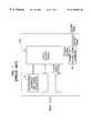
- FIG. 1is a block diagram illustrating a conventional CCD (Charge Coupled Device) image sensor.
- the CCD image sensor 100includes a photoelectric conversion and charge accumulator 10 for absorbing light from an object and collecting the photogenerated charges into signal charge packets.
- the CCD image sensor 100includes a charge transfer region 20 to convey charge packets from the photoelectric conversion and charge accumulator 10 and a charge-to-voltage signal converter 30 to generate a voltage output of the signal charge packets as transferred through the charge transfer region 20 .
- a photodiodeis widely used as a photoelectric conversion and charge accumulator.
- the photodiode having a PN junctionforms a potential well to accumulate the charges generated by light from the object.
- the charges generated in the photoelectric conversion and charge accumulator 10are trapped in the potential well of the photodiode and the trapped charges are transferred to a desired position according to the movement of the potential well. Such a charge movement is controlled by the charge transfer region 20 .
- the charge-to-voltage signal converter 30generates a voltage that is related to the transferred signal charge packets. Since electric charges generate an electric field which corresponds to an electrostatic potential, the change in electric charge concentration as a result of introducing a signal charge packet can be measured by the change in the electrostatic potential (i.e. the depth of the potential well). This potential well depth variation contributes to voltage detection in the CCD image sensor.
- the charges in the current potential wellmust be removed for subsequent signal detections. This removal of the charges is achieved by flushing the signal charge packet into a drain. By lowering the potential barrier between the potential well and the drain, the potential well can be “reset”.
- the conventional CCD image sensordetects the image signals through the charge coupling.
- the photodiodewhich acts as a photosensitive plate corresponding to an image pixel, does not immediately extract photoelectric current, but extracts it after the charges are accumulated for a predetermined time into a signal packet. Accordingly, the CCD image sensor has a good sensitivity with low noise.
- the required driving signalsare very complicated, require large voltage swings of approximately 8V to 10V, have high power consumption, and require both positive and negative power supply.
- CCD technologyis more complicated and also more expensive due to additional photomask processes (about 30 to 40 photomasks).
- the CCD image sensor chipcan not be integrated with signal processing circuitry which is typically implemented by CMOS circuitry, it is very difficult to miniaturize the size of the image sensor and implement in a wider variety of applications.
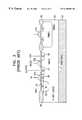
- FIG. 2is a circuit diagram illustrating a unit pixel of the conventional APS proposed by U.S. Pat. No. 5,471,515 of Fossum, et al.
- the APSuses a photogate 21 of the MOS capacitor structure to collect photoelectric charges.
- the APSincludes a transfer transistor 23 .
- the APSincludes a reset transistor 24 , a drain diffusion region 25 , a drive transistor 26 acting as a source follower, a select transistor 27 to select a pixel array row, and a load transistor 28 .
- the MOS capacitorwhich acts as a photosensitive plate, is made of a thick polysilicon layer so that a large fraction of blue light (with a shorter wavelength than red light) is preferentially absorbed by the polysilicon. As a result, it is difficult to obtain high quality color images at low illumination.
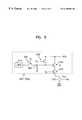
- FIG. 3is a cross-sectional view of the APS proposed by U.S. Pat. No. 5,625,210 of Lee, et al.
- U.S. Pat. No. 5,625,210disclosed the APS with a well-known pinned photodiode.
- the APS in FIG. 3includes a pinned photodiode (PPD) to collect the photoelectric charges and a transfer transistor T x having an N ⁇ region 36 for transferring the photoelectric charges from the PPD to a floating N + region 37 of an output node.
- PPDpinned photodiode
- T xhaving an N ⁇ region 36 for transferring the photoelectric charges from the PPD to a floating N + region 37 of an output node.
- a reset transistorhaving the N + region 37 for one active region and also having an N + region 38 for another active region coupled to a power supply VDD.
- the impuritiesare introduced into a lightly doped P-epi (epitaxial) layer 32 which is grown on a more heavily doped P-type substrate 31 .
- the PPDis formed by a buried N + region 33 and a P + pinning region 34 .
- each of the reference numerals 35 a, 35 b and 35 cdenote a transistor gate.
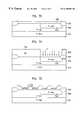
- the PPDis formed by sequential ion implantation of N + and P + impurities, using a single mask layer 41 (e.g., photoresist pattern).
- the PPDis formed by only one mask for both N + and P + ion implantation processes.
- an object of the present inventionto provide an image sensor which can operate at low voltage.
- Another object of the present inventionis to provide a method for fabricating an image sensor using a submicron CMOS technology.
- a further object of the present inventionis to provide an image sensor with improved charge transfer efficiency using an equivalent potential diode.
- a CMOS image sensing devicecomprising: a semiconductor layer of a first conductive type; a well region of the first conductive type, being locally positioned at the semiconductor layer; a photodiode formed in the semiconductor layer for sensing light from an object; at least one depletion transistor formed in the semiconductor layer for transferring photoelectric charges generated in the photodiode to a floating junction which is formed on a portion of the semiconductor layer and which stores the photoelectric charges; and at least one enhancement transistor formed in the well region for outputting electrical signals in response to an amount of the photoelectric charges transferred from the floating junction.
- a CMOS image sensing devicecomprising: a semiconductor layer of a first conductive type; a well region of the first conductive type, being locally positioned at the semiconductor layer; at least one photodiode formed in the semiconductor layer and outside of the well region for sensing light from an object; a floating junction for storing photoelectric charges generated in the photodiode; a first depletion transistor formed outside of the well region and between the photodiode and the floating junction for transferring the photoelectric charges to the floating junction, and wherein the first depletion transistor is controlled in response to a first control signal; a second depletion transistor formed outside of the well region and coupled to the floating junction for resetting the floating junction to a predetermined potential; a first enhancement transistor formed in the well region and for outputting electrical signals in response to an amount of the photoelectric charges stored in the floating junction, wherein a common active region of the second depletion transistor and the first enhancement transistor is positioned at a boundary between the semiconductor
- FIG. 1is a block diagram illustrating a conventional CCD image sensor
- FIG. 2is a circuit diagram illustrating a unit pixel of the conventional APS
- FIGS. 3 and 4are cross-sectional views illustrating the conventional APS of FIG. 2;
- FIG. 5is a circuit diagram illustrating a unit pixel of a CMOS image sensor according to the present invention.
- FIG. 6is a cross-sectional view illustrating a unit pixel of a CMOS image sensor according to the present invention.
- FIGS. 7A to 7 Jare cross-sectional views illustrating a method for fabricating the unit pixel of FIG. 6.
- FIGS. 8A and 8Bare top views of mask patterns used to implant impurity ions into an active region.
- the unit pixelincludes a low-voltage photodiode (LVPD) 510 and four NMOS transistors.
- a transfer transistor (T x ) 520transfers photoelectric charge collected by the low-voltage photodiode 510 for sensing on a floating node 560 .
- a reset transistor (R x ) 530resets the floating node 560 by flushing charges and setting the potential of the node to a known value.
- a drive transistor (D x ) 540acts as a source follower buffer amplifier, and a select transistor 550 provides addressing capability to a common load transistor (S x ) 570 .
- the present inventionhas the important advantage in that the image sensor including the low-voltage photodiode 510 and NMOS transistors can be fabricated using common CMOS technology. Also, the transfer transistor (T x ) 520 and the reset transistor (R x ) 530 are formed as depletion mode or low threshold voltage NMOS transistors in order to improve the charge transfer efficiency and reduce any voltage drop and/or loss of signal charge in the output signal.
- a suitable NMOS transistorcan be fabricated by using the P-epi layer without the P-well. This negative NMOS transistor may have a slightly negative threshold voltage.
- FIG. 6is a cross-sectional view illustrating the unit pixel of the CMOS image sensor according to the present invention.
- an epitaxial layeris used to build CMOS devices in the present invention. Namely, a wafer having a P-epi layer 602 , which is formed on a P + substrate 601 to an impurity concentration of approximately 10 14 ions/cm 3 , is used.
- the P-epi layer 602is used for the following reasons:
- the P-epi layer 602allows the depletion region of the low-voltage photodiode to be large and deep which improves the sensitivity by increasing the ability of the low-voltage photodiode in collecting photogenerated charges.
- the thickness of the P-epi layer 602is in a range of approximately 2 to 5 ⁇ m.
- the highly doped P substrate 601 beneath the P-epi layer 602improves the sensor array modulation transfer function by reducing the random diffusion of the photoelectric charges.
- the random diffusion of charges in the P-type substrateleads to the possible “miscollection” of the photogenerated charges by neighboring pixels and directly results in a loss of image sharpness or a lower modulation transfer function.
- the shorter minority carrier lifetime and higher doping concentration of the P + substrate 601significantly reduces the “miscollection” of photoelectric charges since the charges are quickly recombined before diffusing to the neighboring pixels.
- the P + substrate 601 and the P-epi layer 602have resistivity of about 0.01 ⁇ cm and 10-25 ⁇ cm, respectively. Accordingly, the impurity concentration of the P + substrate 601 should be much higher than that of the P-epi layer 602 and the corresponding minority carrier lifetime of the P + substrate 601 should be much lower than that of the P-epi layer 602 .
- the low-voltage photodiodeincludes a lightly doped N ⁇ region 603 formed in the P-epi layer 602 and a lightly doped P 0 region 604 formed about the lightly doped N ⁇ region 603 .
- This low-voltage photodiodehas excellent sensitivity and photon-to-electron quantum efficiency since the light sensing region is not covered with a polysilicon layer. In particular, the sensitivity of short wavelength, blue light, is significantly improved.
- the lightly doped P-epi layerthe charge depletion region of the low-voltage photodiode also has high sensitivity for long wavelength, red or infrared light.
- this low-voltage photodiodehas the ability to rapidly and efficiently transfer charge to the floating sensing node from the light sensing region. Furthermore, dark current is decreased by controlling the potential of interface generation states at the silicon-silicon dioxide interface.
- the low-voltage photodiodeshould be fully depleted at a low voltage which is compatible with a power supply of 5V, 3.3V or 2.5V.
- the conventional CCDsrequire high driving voltage in excess of 8V in order to effectively transfer charges and fully deplete the buried photodiode fabricated in a typical CCD process. Due to high temperature processes after ion implantation of the buried photodiode in a CCD process, the resulting buried photodiode can not be fully depleted at a voltage of less than 5V. Also, buried photodiodes using inclined ion implantation techniques can not be stably implemented by a typical submicron CMOS process which utilizes the low-temperature processes.
- CMOS process for 3.3V operationshould have a buried photodiode structure which is fully depleted in the range of 1.2V-2.8V. If this voltage is too high, incomplete charge transfer of the photoelectric charges to the floating sensing node will cause many undesirable imaging artifacts. On the other hand, if this voltage is too low, the charge capacity of the buried photodiode will be very low resulting in a small output signal.
- the present inventionfabricates a low-voltage photodiode which can be fully depleted at a voltage range of 1.2V-4.5V in the case of the power supply of 3.3V and 5V.
- a low-voltage photodiodewhich can be fully depleted at a voltage range of 1.2V-4.5V in the case of the power supply of 3.3V and 5V.
- FIG. 6because the edge of a field oxide layer 607 and the edge of the N ⁇ region 603 are sufficiently spaced apart (see “A” in FIG. 6 ), the P 0 region 604 is electrically connected to the P-epi layer 602 and is insured to be at the same potential.
- the N ⁇ layer 603can be reliably fully depleted at a voltage between 1.2V-4.5V.
- the transfer transistor (T x ) and the reset transistor (R x )are low threshold voltage or depletion mode transistors to insure a full reset of the floating node and maximize the output voltage dynamic range.
- the drive transistor (D x ) and the select transistor (S x )are typical NMOS transistors. Accordingly, the drive transistor (D x ) and the select transistor (S x ) are formed in the P-well. However, a lateral well diffusion within the pixel causes the electrical characteristics of the low-voltage photodiode and the native transistors to deteriorate.
- the P-well 605is limited to a small area but, through a lateral diffusion, incorporates all the drive and select transistors without impacting the low-voltage photodiode and associated reset and transfer transistors.
- the P-well regionincludes a portion of the drain 606 of the reset transistor (R x ) and extends to the field oxide layer 607 (hereinafter, this P-well 605 is referred to as a mini P-well).
- the drive transistor (D x ) and the select transistor (S x ) formed in the P-well 605use the LDD (Lightly Doped Drain) structure.
- the transfer transistor (T x ) and the reset transistor (R x ) formed in the P-epi layer 602do not use the LDD (Lightly Doped Drain) structure, which improves the isolation of the floating node from the reset voltage, reduces the amount of coupling between the reset and transfer clock signal by reducing the overlap capacitance, and increases the overall sensitivity of the pixel by reducing the total capacitance associated with the floating node.
- LDDLightly Doped Drain
- the floating sensing nodeis reset by turning on the reset transistor (R x ).
- the unit pixelis selected for read out by turning on the select transistor (S x ).
- the output voltage V 2 of the source follower bufferis measured.
- the resulting difference output signal, V 1 -V 2is due to the transfer of photoelectric charges.
- This methodis called the CDS (Correlated Double Sampling) method and provides for cancellation of offset voltage, reset switch noise and 1/f flicker noise.
- FIGS. 7A to 7 Jare cross-sectional views illustrating a method for fabricating the unit pixel of the CMOS image sensor according to the present invention.
- a P-epi layer 702is formed on a P + substrate 701 and impurities are introduced into the exposed P-epi layer.
- impuritiesare introduced into the exposed P-epi layer.
- a conventional P-well substrate as found in a typical submicron CMOS processis not used for the CMOS image sensor of the present invention.
- the conventional well structure as found in a typical submicron CMOS processwill degrade the electrical characteristics of the low-voltage photodiode and the native NMOS transistors due to the limited tolerance for lateral dopant diffusion within the small pixel. That is, as illustrated above, the mini P-well process is carried out.
- a P-well 705which incorporates both the drive and select transistors is formed by the lateral diffusion during thermal treatment.
- a field oxide layer 707 to define a field region and an active regionis formed by the LOCOS process, the trench isolation process or similar process.
- a multilayer mask pattern 706 where a pad oxide layer, buffer polysilicon layer and a nitride layer are formed in this orderis used as a wet oxidation mask for forming the field oxide layer.
- the isolationis well-known to those of ordinary skill in the art to which the subject matter pertains.
- a mask pattern 740 to expose the P-well 705is formed and an ion implantation is carried out to adjust the N-channel threshold voltage and the punchthrough.
- an ion implantationis carried out to adjust the N-channel threshold voltage and the punchthrough.
- a polysilicon layer 709 and a tungsten silicide layer 710are, in this order, formed on the P-epi layer 702 and patterned by mask and etching processes, thereby forming four gate electrodes 711 which are spaced a predetermined distance apart.
- a mask pattern 713is formed on the resulting structure to form a lightly doped N ⁇ region 721 of the low-voltage photodiode and impurities are introduced into the P-epi layer 702 at a concentration of approximately 10 17 ions/cm 3 .
- impuritiesare introduced into the P-epi layer 702 at a concentration of approximately 10 17 ions/cm 3 .
- one end 715 of the mask pattern 713is positioned in the middle of the gate electrode of the transfer transistor and the other end 716 thereof is positioned inside the active region.
- the interface between the field region and the active regionis covered with the mask pattern 713 so that a portion of the active region, which is in the neighborhood of the interface, is not applied to the ion implantation.
- the mask pattern 713is taken along line A-A′ of a photomask in FIG. 8 A.
- the mask pattern 713is aligned along an interface (dotted lines in FIG. 8A) between the active region and the field region but it covers a portion 800 of the active region, thereby preventing N ⁇ impurity ions from being introduced into the edge thereof.
- the mask pattern 713is removed and another mask pattern 717 is formed to form a lightly doped P 0 region 722 .
- the impuritiesare introduced into the P-epi layer 702 at a concentration of approximately 10 18 ions/cm 3 .
- the acceleration energy of the P 0 ionsis lower than that of N ⁇ ions of FIG. 7F so that the lightly doped P 0 region 722 is positioned on the lightly doped N ⁇ region 721 .
- one end 719 of the mask pattern 717is positioned in the middle of the gate electrode of the transfer transistor and the other end 720 thereof is positioned on the field oxide layer 707 .
- FIG. 8Bshows a top view of the mask pattern 717 . Accordingly, the entire active region of the low-voltage photodiode of the present invention is exposed so that a sufficient electrical connection A is achieved between the P 0 region 722 and the P-epi layer 702 , compared with the electrical connection shown in FIG. 3 .
- the present inventionemploys two masks of different sizes, it should be noted that such a connection A can be achieved by controlling the depth of the impurity regions.
- the thickness of the gate electrode of the transfer transistormust be controlled. Since the doping profile of the low-voltage photodiode determines the charge transfer efficiency, the doping area is self-aligned with the one end of the gate electrode of the transfer transistor. Accordingly, the gate electrode of the transfer transistor must have such a thickness as to block the accelerated ions. If not, the ions penetrate into the gate electrode so that the ion doped layers 721 and 722 are not self-aligned with the edge of the gate electrode of the transfer transistor. This misalignment degrades the charge transfer efficiency.
- the polysilicon layer and the tungsten silicide layerare formed at a thickness of about 1500 ⁇ and below 1500 ⁇ , respectively, in the conventional CMOS process, but in the preferred embodiment of the present invention they are formed at a thickness of above 2000 ⁇ and above 1500 ⁇ , respectively.
- the thickness of the gate electrode of the transfer transistor according to the present inventionis relatively thicker than that of the NMOS transistor fabricated by the conventional CMOS processes.
- the edge of the lightly doped N ⁇ region 721is apart from the edge of the field oxide layer 707 and the sufficient electrical connection A is achieved between the P 0 region 722 and the P-epi layer 702 , the P 0 region 722 and the P-epi layer 702 have the same potential even at a supply voltage below 5V. Accordingly, the lightly doped N ⁇ region 721 should be fully depleted at 1.2-4.5V. If sufficient electrical connection A between the P 0 region 722 and the P-epi layer 702 is not achieved, the photodiode may not act as a low-voltage photodiode and not achieve a full depletion.
- a mask pattern 723is formed on the resulting structure, exposing the P-well region in order to provide the drive and select transistors with the LDD structure.
- the drive and select transistors in the P-wellwill have the same characteristics as the conventional submicron NMOS transistors. Since this ion implantation for LDD structure is not carried out in the P-epi layer 702 , the transfer and reset transistors do not have the LDD structure, i.e., native NMOS transistors.
- an oxide layeris deposited on the resulting structure by the LPCVD (Low Pressure Chemical Vapor Deposition) method in order to form source/drain regions of the four transistors within the unit pixel.
- the etchback processis applied to the oxide layer and then oxide spacer layers 726 are formed on the sidewalls of all the transistors.
- a mask pattern 727 for implanting impurity ions into P-epi layer 702 and the P-well 705except for the low-voltage photodiode area, is formed on the resulting structure and N + ion implantation is carried out, thereby forming highly doped N + regions 729 for source/drains.
- the native transistors T x and R x formed on the P-epi layer 702have a negative threshold voltage (depletion mode).
- the characteristics of the native depletion mode transistorare effectively used in the transfer transistor of the present invention. For example, when the charge capacity of the photodiode is reached, excess photoelectric charges will overflow the photodiode and be collected by neighboring pixels. The resulting cross-talk from an intense light source in an image is called “Blooming.”
- the self-aligned N ⁇ region 721 and P 0 region 722 within the low-voltage photodiodeundergo the out-diffusion process through the high-temperature LPCVD process for forming the oxide spacer layers 726 .
- a potential barrierwhich decreases the charge transfer efficiency, is created at one side of the transfer transistor. Accordingly, in order to avoid creation of this undesired potential barrier at the time of performing the high-temperature LPCVD process, the lateral profile of the P 0 and N ⁇ regions 722 and 721 is carefully controlled.
- FIG. 7Jis a cross-sectional view of the unit pixel after the general back-end processes.
- interlayer insulating layers PMD, IMD 1 and IMD 2 and metal layers M 1 and M 2are formed and a passivation layer is formed for protecting the device from moisture and scratches.
- a color filter arrayconsisting of red, green and blue color arrangement or yellow, magenta and cyan color arrangement is formed on the passivation layer.
- insulating layer, passivation layer and color filtermay be used.
Landscapes
- Solid State Image Pick-Up Elements (AREA)
- Light Receiving Elements (AREA)
- Transforming Light Signals Into Electric Signals (AREA)
Abstract
Description
Claims (20)
Applications Claiming Priority (2)
| Application Number | Priority Date | Filing Date | Title |
|---|---|---|---|
| KR98-6687 | 1998-02-28 | ||
| KR19980006687 | 1998-02-28 |
Publications (1)
| Publication Number | Publication Date |
|---|---|
| US6180969B1true US6180969B1 (en) | 2001-01-30 |
Family
ID=19534037
Family Applications (2)
| Application Number | Title | Priority Date | Filing Date |
|---|---|---|---|
| US09/258,814Expired - LifetimeUS6184055B1 (en) | 1998-02-28 | 1999-02-26 | CMOS image sensor with equivalent potential diode and method for fabricating the same |
| US09/258,307Expired - LifetimeUS6180969B1 (en) | 1998-02-28 | 1999-02-26 | CMOS image sensor with equivalent potential diode |
Family Applications Before (1)
| Application Number | Title | Priority Date | Filing Date |
|---|---|---|---|
| US09/258,814Expired - LifetimeUS6184055B1 (en) | 1998-02-28 | 1999-02-26 | CMOS image sensor with equivalent potential diode and method for fabricating the same |
Country Status (9)
| Country | Link |
|---|---|
| US (2) | US6184055B1 (en) |
| JP (1) | JP4390896B2 (en) |
| KR (1) | KR100278285B1 (en) |
| CN (2) | CN1171315C (en) |
| DE (1) | DE19908457B4 (en) |
| FR (2) | FR2775541B1 (en) |
| GB (1) | GB2334817B (en) |
| NL (2) | NL1011381C2 (en) |
| TW (1) | TW457644B (en) |
Cited By (46)
| Publication number | Priority date | Publication date | Assignee | Title |
|---|---|---|---|---|
| US6369417B1 (en)* | 2000-08-18 | 2002-04-09 | Hyundai Electronics Industries Co., Ltd. | CMOS image sensor and method for fabricating the same |
| US6388243B1 (en)* | 1999-03-01 | 2002-05-14 | Photobit Corporation | Active pixel sensor with fully-depleted buried photoreceptor |
| US6465846B1 (en)* | 2000-03-22 | 2002-10-15 | Seiko Instruments Inc. | Semiconductor integrated circuit device having trench-type photodiode |
| US6541329B1 (en)* | 2001-09-07 | 2003-04-01 | United Microelectronics Corp. | Method for making an active pixel sensor |
| US6566697B1 (en) | 2000-11-28 | 2003-05-20 | Dalsa, Inc. | Pinned photodiode five transistor pixel |
| US6593175B2 (en)* | 2000-10-24 | 2003-07-15 | Advanced Micro Devices, Inc. | Method of controlling a shape of an oxide layer formed on a substrate |
| US20030197228A1 (en)* | 2002-03-07 | 2003-10-23 | Fujitsu Limited | CMOS image sensor and method of fabricating the same |
| US20030234432A1 (en)* | 2002-06-20 | 2003-12-25 | Samsung Electronics Co., Ltd. | Image sensor and method of fabricating the same |
| US6670205B1 (en) | 2002-09-18 | 2003-12-30 | Hynix Semiconductor Inc | Method of fabricating image sensor equipped with lens |
| US6706550B2 (en)* | 1998-06-27 | 2004-03-16 | Hyundai Electronics Industries Co, Ltd. | Photodiode having a plurality of PN injections and image sensor having the same |
| US6713796B1 (en) | 2001-01-19 | 2004-03-30 | Dalsa, Inc. | Isolated photodiode |
| US20040119864A1 (en)* | 2002-12-03 | 2004-06-24 | Canon Kabushiki Kaisha | Photoelectric conversion device and image pick-up system using the photoelectric conversion device |
| US20040129990A1 (en)* | 2002-12-27 | 2004-07-08 | Ju-Il Lee | Method for manufacturing CMOS image sensor using spacer etching barrier film |
| US6764890B1 (en) | 2003-01-29 | 2004-07-20 | Cypress Semiconductor Corporation | Method of adjusting the threshold voltage of a mosfet |
| US20040169209A1 (en)* | 1999-03-08 | 2004-09-02 | Vladimir Berezin | Multi junction APS with dual simultaneous integration |
| US20040188728A1 (en)* | 2003-02-21 | 2004-09-30 | Stmicroelectronics Ltd. | CMOS image sensors |
| US20040222481A1 (en)* | 2003-04-10 | 2004-11-11 | Rhodes Howard E. | Imager light shield |
| EP1501129A1 (en)* | 2003-07-22 | 2005-01-26 | OmniVision Technologies, Inc. | Active pixel cell using negative to positive voltage swing transfer transistor |
| US20050017245A1 (en)* | 2003-07-22 | 2005-01-27 | Sohei Manabe | CMOS image sensor formed on an N-type substrate |
| US20050036051A1 (en)* | 1998-06-08 | 2005-02-17 | Takahisa Ueno | Solid-state imaging element, method for driving the same, and camera system |
| US20050041129A1 (en)* | 2003-08-23 | 2005-02-24 | Yo-Jong Kim | CMOS image sensor and method for sensing an image using the same |
| US20050067640A1 (en)* | 2003-09-26 | 2005-03-31 | Fujitsu Limited | Imaging device and manufacturing method thereof |
| US20050139878A1 (en)* | 2003-12-31 | 2005-06-30 | Dongbuanam Semiconductor Inc. | CMOS image sensor and method for fabricating the same |
| US20060141661A1 (en)* | 2002-09-11 | 2006-06-29 | Park Young-Hoon | CMOS image sensor and method of fabricating the same |
| US20060186505A1 (en)* | 2005-02-23 | 2006-08-24 | International Business Machines Corporation | Image sensor cells |
| US20060186547A1 (en)* | 2005-02-24 | 2006-08-24 | Wen-De Wang | Light shield for CMOS imager |
| US20060226339A1 (en)* | 2005-04-11 | 2006-10-12 | Samsung Electronics Co., Ltd. | CMOS image sensor and method of fabricating the same |
| US20060226438A1 (en)* | 2005-04-11 | 2006-10-12 | Matsushita Electric Industrial Co., Ltd. | Solid-state imaging device |
| US20060261431A1 (en)* | 2005-05-18 | 2006-11-23 | Samsung Elctronics Co., Ltd. | Pixels for CMOS image sensors |
| US20080001192A1 (en)* | 2005-03-11 | 2008-01-03 | Fujitsu Limited | Image sensor with embedded photodiode region and manufacturing method for same |
| US20080054321A1 (en)* | 2006-08-31 | 2008-03-06 | Dongbu Hitek Co., Ltd. | CMOS image sensor and method for manufacturing the same |
| US20080176350A1 (en)* | 2004-01-06 | 2008-07-24 | Rhodes Howard E | Method and apparatus providing CMOS imager device pixel with transistor having lower threshold voltage than other imager device transistors |
| US20090001434A1 (en)* | 2004-11-03 | 2009-01-01 | X-Fab Semiconductor Foundries Ag | Vertical Pin or Nip Photodiode and Method for the Production which is Compatible with a Conventional Cmos-Process |
| US20120007156A1 (en)* | 2007-01-31 | 2012-01-12 | Taiwan Semiconductor Manufacturing Company, Ltd. | Method and structure to reduce dark current in image sensors |
| US20120235022A1 (en)* | 2005-09-02 | 2012-09-20 | Sony Corporation | Solid-state imaging device, drive method of solid-state imaging device, and imaging apparatus |
| US20120270364A1 (en)* | 2009-07-31 | 2012-10-25 | Fujitsu Semiconductor Limited | Semiconductor device and method for producing same |
| US20150103009A1 (en)* | 2013-10-14 | 2015-04-16 | Pixart Imaging Inc. | Image sensing apparatus and optical navigating apparatus with the image sensing apparatus |
| US9343489B2 (en) | 2011-05-12 | 2016-05-17 | DePuy Synthes Products, Inc. | Image sensor for endoscopic use |
| US9462234B2 (en) | 2012-07-26 | 2016-10-04 | DePuy Synthes Products, Inc. | Camera system with minimal area monolithic CMOS image sensor |
| US10206561B2 (en) | 2013-02-28 | 2019-02-19 | DePuy Synthes Products, Inc. | Videostroboscopy of vocal cords with CMOS sensors |
| US10517469B2 (en) | 2013-03-15 | 2019-12-31 | DePuy Synthes Products, Inc. | Image sensor synchronization without input clock and data transmission clock |
| US10750933B2 (en) | 2013-03-15 | 2020-08-25 | DePuy Synthes Products, Inc. | Minimize image sensor I/O and conductor counts in endoscope applications |
| US20200412986A1 (en)* | 2019-06-28 | 2020-12-31 | Stmicroelectronics (Crolles 2) Sas | Pixel and method for controlling the same |
| CN112447775A (en)* | 2019-08-28 | 2021-03-05 | 天津大学青岛海洋技术研究院 | CMOS image sensor pixel manufacturing method for improving quantum efficiency |
| US11156700B2 (en)* | 2016-05-02 | 2021-10-26 | Hamamatsu Photonics K.K. | Distance sensor |
| CN114203625A (en)* | 2020-09-02 | 2022-03-18 | 长鑫存储技术有限公司 | Semiconductor device and method for manufacturing the same |
Families Citing this family (106)
| Publication number | Priority date | Publication date | Assignee | Title |
|---|---|---|---|---|
| JPH11264761A (en)* | 1998-03-18 | 1999-09-28 | Honda Motor Co Ltd | Optical sensor circuit and image sensor using the same |
| JP3571909B2 (en)* | 1998-03-19 | 2004-09-29 | キヤノン株式会社 | Solid-state imaging device and method of manufacturing the same |
| JP3457551B2 (en)* | 1998-11-09 | 2003-10-20 | 株式会社東芝 | Solid-state imaging device |
| US6590242B1 (en)* | 1999-02-25 | 2003-07-08 | Canon Kabushiki Kaisha | Light-receiving element and photoelectric conversion device |
| JP3576033B2 (en)* | 1999-03-31 | 2004-10-13 | 株式会社東芝 | Solid-state imaging device |
| US6310366B1 (en)* | 1999-06-16 | 2001-10-30 | Micron Technology, Inc. | Retrograde well structure for a CMOS imager |
| US6333205B1 (en)* | 1999-08-16 | 2001-12-25 | Micron Technology, Inc. | CMOS imager with selectively silicided gates |
| US6593607B1 (en)* | 1999-09-30 | 2003-07-15 | Pictos Technologies, Inc. | Image sensor with enhanced blue response and signal cross-talk suppression |
| US6410905B1 (en)* | 1999-12-17 | 2002-06-25 | Scientific Imaging Technologies, Inc. | CCD with enhanced output dynamic range |
| KR100390822B1 (en)* | 1999-12-28 | 2003-07-10 | 주식회사 하이닉스반도체 | Method for reducing dark current in image sensor |
| US6407440B1 (en)* | 2000-02-25 | 2002-06-18 | Micron Technology Inc. | Pixel cell with high storage capacitance for a CMOS imager |
| KR100359770B1 (en)* | 2000-03-02 | 2002-11-04 | 주식회사 하이닉스반도체 | Active pixel circuit in CMOS image sensor |
| JP2001298663A (en)* | 2000-04-12 | 2001-10-26 | Semiconductor Energy Lab Co Ltd | Semiconductor device and its drive method |
| JP3664939B2 (en)* | 2000-04-14 | 2005-06-29 | 富士通株式会社 | CMOS image sensor and manufacturing method thereof |
| KR100386609B1 (en)* | 2000-04-28 | 2003-06-02 | 주식회사 하이닉스반도체 | CMOS image sensor and method for fabricating the same |
| US6429499B1 (en)* | 2000-05-18 | 2002-08-06 | International Business Machines Corporation | Method and apparatus for a monolithic integrated MESFET and p-i-n optical receiver |
| JP3688980B2 (en)* | 2000-06-28 | 2005-08-31 | 株式会社東芝 | MOS type solid-state imaging device and manufacturing method thereof |
| TW449939B (en)* | 2000-07-03 | 2001-08-11 | United Microelectronics Corp | Photodiode structure |
| DE60144528D1 (en)* | 2000-10-19 | 2011-06-09 | Quantum Semiconductor Llc | METHOD FOR PRODUCING CMOS INTEGRATED HETEROVER PHOTODODMS |
| JP4270742B2 (en) | 2000-11-30 | 2009-06-03 | Necエレクトロニクス株式会社 | Solid-state imaging device |
| KR100521972B1 (en)* | 2000-12-30 | 2005-10-17 | 매그나칩 반도체 유한회사 | Image sensor having power supply line connect to light sensing region |
| KR20020096336A (en)* | 2001-06-19 | 2002-12-31 | 삼성전자 주식회사 | Cmos type image sensor |
| US6765276B2 (en)* | 2001-08-23 | 2004-07-20 | Agilent Technologies, Inc. | Bottom antireflection coating color filter process for fabricating solid state image sensors |
| US6545303B1 (en)* | 2001-11-06 | 2003-04-08 | Fillfactory | Method to increase conversion gain of an active pixel, and corresponding active pixel |
| US6462365B1 (en)* | 2001-11-06 | 2002-10-08 | Omnivision Technologies, Inc. | Active pixel having reduced dark current in a CMOS image sensor |
| JP3781672B2 (en)* | 2001-12-14 | 2006-05-31 | 株式会社東芝 | Solid-state imaging device |
| JP3723124B2 (en)* | 2001-12-14 | 2005-12-07 | 株式会社東芝 | Solid-state imaging device |
| KR20030052588A (en)* | 2001-12-21 | 2003-06-27 | 주식회사 하이닉스반도체 | Image sensor with enhanced charge transfer rate and method for fabricating the same |
| KR100462164B1 (en)* | 2002-01-11 | 2004-12-17 | 매그나칩 반도체 유한회사 | Cmos image sensor with enhanced fill factor |
| US6730900B2 (en)* | 2002-02-05 | 2004-05-04 | E-Phocus, Inc. | Camera with MOS or CMOS sensor array |
| JP4412903B2 (en)* | 2002-06-24 | 2010-02-10 | 株式会社ルネサステクノロジ | Semiconductor device |
| KR100893054B1 (en)* | 2002-07-05 | 2009-04-15 | 매그나칩 반도체 유한회사 | Image sensor and its manufacturing method that can prevent crosstalk |
| US6906302B2 (en)* | 2002-07-30 | 2005-06-14 | Freescale Semiconductor, Inc. | Photodetector circuit device and method thereof |
| CN100431160C (en) | 2002-09-12 | 2008-11-05 | 松下电器产业株式会社 | Solid-state imaging device and manufacturing method thereof |
| US6586789B1 (en)* | 2002-10-07 | 2003-07-01 | Lixin Zhao | Pixel image sensor |
| KR20040036049A (en)* | 2002-10-23 | 2004-04-30 | 주식회사 하이닉스반도체 | CMOS Image sensor improved fill factor |
| KR100669645B1 (en)* | 2002-11-12 | 2007-01-16 | 마이크론 테크놀로지, 인크 | Ground Gate and Isolation Technology to Reduce Dark Current in CMOS Image Sensors |
| US6818930B2 (en)* | 2002-11-12 | 2004-11-16 | Micron Technology, Inc. | Gated isolation structure for imagers |
| KR100461975B1 (en)* | 2002-12-27 | 2004-12-17 | 매그나칩 반도체 유한회사 | Method for forming trench isolation layer in image sensor |
| US6730899B1 (en)* | 2003-01-10 | 2004-05-04 | Eastman Kodak Company | Reduced dark current for CMOS image sensors |
| JP4281375B2 (en)* | 2003-02-19 | 2009-06-17 | ソニー株式会社 | CMOS solid-state imaging device and driving method thereof |
| KR100949666B1 (en)* | 2003-04-29 | 2010-03-29 | 매그나칩 반도체 유한회사 | Method of manufacturing semiconductor device |
| KR100523671B1 (en) | 2003-04-30 | 2005-10-24 | 매그나칩 반도체 유한회사 | Cmos image sensor with double gateoxide and method of fabricating the same |
| US6900484B2 (en)* | 2003-07-30 | 2005-05-31 | Micron Technology, Inc. | Angled pinned photodiode for high quantum efficiency |
| KR100544957B1 (en)* | 2003-09-23 | 2006-01-24 | 동부아남반도체 주식회사 | Manufacturing Method of CMOS Image Sensor |
| US7354789B2 (en)* | 2003-11-04 | 2008-04-08 | Dongbu Electronics Co., Ltd. | CMOS image sensor and method for fabricating the same |
| US7196304B2 (en)* | 2004-01-29 | 2007-03-27 | Micron Technology, Inc. | Row driver for selectively supplying operating power to imager pixel |
| US7037764B2 (en)* | 2004-02-26 | 2006-05-02 | Micron Technology, Inc. | Method of forming a contact in a pixel cell |
| US20050224901A1 (en)* | 2004-03-30 | 2005-10-13 | Xinping He | Active pixel having buried transistor |
| KR100698069B1 (en)* | 2004-07-01 | 2007-03-23 | 동부일렉트로닉스 주식회사 | Manufacturing Method of CMOS Image Sensor |
| KR101115092B1 (en)* | 2004-07-29 | 2012-02-28 | 인텔렉츄얼 벤처스 투 엘엘씨 | Image sensor with improved charge transfer efficiency and method for fabrication thereof |
| KR101069103B1 (en)* | 2004-07-29 | 2011-09-30 | 크로스텍 캐피탈, 엘엘씨 | Image Sensor and Manufacturing Method for Improving Charge Transport Efficiency |
| KR100649023B1 (en)* | 2004-11-09 | 2006-11-28 | 동부일렉트로닉스 주식회사 | Manufacturing Method of CMOS Image Sensor |
| KR100649012B1 (en)* | 2004-12-30 | 2006-11-27 | 동부일렉트로닉스 주식회사 | CMOS image sensor and its manufacturing method for improving color reproducibility |
| KR100606918B1 (en)* | 2004-12-30 | 2006-08-01 | 동부일렉트로닉스 주식회사 | Hot pixel of vertical CMOS image sensor and its manufacturing method |
| KR100640958B1 (en)* | 2004-12-30 | 2006-11-02 | 동부일렉트로닉스 주식회사 | CMOS image sensor using protective film and manufacturing method |
| KR101199100B1 (en)* | 2004-12-30 | 2012-11-08 | 인텔렉츄얼 벤처스 투 엘엘씨 | Cmos image sensor having asymmetric well structure of source follower |
| KR100672708B1 (en)* | 2004-12-30 | 2007-01-22 | 동부일렉트로닉스 주식회사 | Separator Formation Method of CMOS Image Sensor |
| JP4691990B2 (en)* | 2005-01-05 | 2011-06-01 | ソニー株式会社 | Solid-state imaging device and manufacturing method thereof |
| US20060183268A1 (en)* | 2005-02-14 | 2006-08-17 | Omnivision Technologies, Inc. | Salicide process for image sensor |
| JP4224036B2 (en)* | 2005-03-17 | 2009-02-12 | 富士通マイクロエレクトロニクス株式会社 | Image sensor with embedded photodiode region and method of manufacturing the same |
| KR100782463B1 (en)* | 2005-04-13 | 2007-12-05 | (주)실리콘화일 | Separated unit pixel and its manufacturing method of an image sensor having a three-dimensional structure |
| JP4340660B2 (en)* | 2005-04-14 | 2009-10-07 | シャープ株式会社 | Amplification type solid-state imaging device |
| KR100670510B1 (en)* | 2005-04-26 | 2007-01-16 | 매그나칩 반도체 유한회사 | Manufacturing Method of CMOS Image Sensor |
| US7115924B1 (en)* | 2005-06-03 | 2006-10-03 | Avago Technologies Sensor Ip Pte. Ltd. | Pixel with asymmetric transfer gate channel doping |
| KR100672688B1 (en)* | 2005-06-07 | 2007-01-22 | 동부일렉트로닉스 주식회사 | Manufacturing Method of CMOS Image Sensor |
| KR100698090B1 (en)* | 2005-06-07 | 2007-03-23 | 동부일렉트로닉스 주식회사 | CMOS image sensor and its manufacturing method |
| CN100395883C (en)* | 2005-06-28 | 2008-06-18 | 中芯国际集成电路制造(上海)有限公司 | CMOS image sensing device and method using independent source formation |
| KR100718878B1 (en)* | 2005-06-28 | 2007-05-17 | (주)실리콘화일 | Discrete unit pixel of an image sensor having a three-dimensional structure and manufacturing method thereof |
| CN100416845C (en)* | 2005-07-12 | 2008-09-03 | 北京思比科微电子技术有限公司 | Hole accumulation type active pixel with low substrate leakage current and manufacturing method thereof |
| US20070074518A1 (en)* | 2005-09-30 | 2007-04-05 | Solar Turbines Incorporated | Turbine engine having acoustically tuned fuel nozzle |
| KR100752185B1 (en)* | 2005-10-13 | 2007-08-24 | 동부일렉트로닉스 주식회사 | CMOS image sensor and its manufacturing method |
| US7323378B2 (en)* | 2005-10-20 | 2008-01-29 | Pixart Imaging Inc. | Method for fabricating CMOS image sensor |
| JP4848739B2 (en)* | 2005-11-01 | 2011-12-28 | ソニー株式会社 | Physical quantity detection apparatus and imaging apparatus |
| US7633106B2 (en)* | 2005-11-09 | 2009-12-15 | International Business Machines Corporation | Light shield for CMOS imager |
| JP2007228460A (en)* | 2006-02-27 | 2007-09-06 | Mitsumasa Koyanagi | Stacked semiconductor device with integrated sensor |
| JP5016244B2 (en)* | 2006-03-17 | 2012-09-05 | ルネサスエレクトロニクス株式会社 | Semiconductor memory device |
| CN100468699C (en)* | 2006-04-29 | 2009-03-11 | 联华电子股份有限公司 | Image sensing element and manufacturing method thereof |
| KR100776146B1 (en)* | 2006-05-04 | 2007-11-15 | 매그나칩 반도체 유한회사 | CMOS image sensor with improved performance by integrating pixels with burst reset operation |
| KR100757654B1 (en) | 2006-05-26 | 2007-09-10 | 매그나칩 반도체 유한회사 | CMOS image sensor and its manufacturing method |
| KR100801447B1 (en)* | 2006-06-19 | 2008-02-11 | (주)실리콘화일 | Image sensor using back light photodiode and manufacturing method thereof |
| KR100781892B1 (en)* | 2006-08-28 | 2007-12-03 | 동부일렉트로닉스 주식회사 | CMS image sensor and its manufacturing method |
| US7795655B2 (en)* | 2006-10-04 | 2010-09-14 | Sony Corporation | Solid-state imaging device and electronic device |
| KR100782312B1 (en) | 2006-10-25 | 2007-12-06 | 한국전자통신연구원 | High Definition CMOS Image Sensors and Photodiodes |
| KR100880528B1 (en)* | 2007-06-01 | 2009-01-28 | 매그나칩 반도체 유한회사 | CMOS image sensor |
| KR100871792B1 (en)* | 2007-06-26 | 2008-12-05 | 주식회사 동부하이텍 | Image sensor and manufacturing method |
| KR20090003854A (en)* | 2007-07-05 | 2009-01-12 | 삼성전자주식회사 | Image sensor and its manufacturing method |
| KR100871798B1 (en)* | 2007-09-07 | 2008-12-02 | 주식회사 동부하이텍 | Image sensor and its manufacturing method |
| JP2009117613A (en)* | 2007-11-06 | 2009-05-28 | Toshiba Corp | Semiconductor device |
| KR100882468B1 (en)* | 2007-12-28 | 2009-02-09 | 주식회사 동부하이텍 | Image sensor and manufacturing method |
| JP2009088545A (en)* | 2008-11-28 | 2009-04-23 | Nec Electronics Corp | Solid-state image pick-up device |
| JP5446282B2 (en)* | 2009-01-21 | 2014-03-19 | ソニー株式会社 | Solid-state imaging device and camera system |
| JP2010278303A (en)* | 2009-05-29 | 2010-12-09 | Toshiba Corp | Solid-state imaging device |
| US9698196B2 (en)* | 2009-08-14 | 2017-07-04 | Heptagon Micro Optics Pte. Ltd. | Demodulation pixel incorporating majority carrier current, buried channel and high-low junction |
| JP5351066B2 (en)* | 2010-01-25 | 2013-11-27 | 浜松ホトニクス株式会社 | OCT equipment |
| JP6119454B2 (en)* | 2013-06-24 | 2017-04-26 | 富士通セミコンダクター株式会社 | Method for manufacturing semiconductor device and method for measuring semiconductor device |
| JP6892221B2 (en)* | 2016-03-04 | 2021-06-23 | エイブリック株式会社 | Manufacturing method of semiconductor devices |
| RU2634324C1 (en)* | 2016-05-18 | 2017-10-25 | Публичное акционерное общество "Интерсофт Евразия", ПАО "Интерсофт Евразия" | Ionizing radiation sensor based on silicon of crucible-free melting zone of p-type conductivity |
| KR102617389B1 (en)* | 2016-10-06 | 2023-12-26 | 에스케이하이닉스 주식회사 | Image sensor |
| CN106565930A (en)* | 2016-11-08 | 2017-04-19 | 武汉理工大学 | Phosphorus flame retardant and all water blown phosphorus containing flame retardant polyurethane foam based on same |
| US10616519B2 (en) | 2016-12-20 | 2020-04-07 | Microsoft Technology Licensing, Llc | Global shutter pixel structures with shared transfer gates |
| US10389957B2 (en) | 2016-12-20 | 2019-08-20 | Microsoft Technology Licensing, Llc | Readout voltage uncertainty compensation in time-of-flight imaging pixels |
| TWI621273B (en)* | 2017-04-27 | 2018-04-11 | 立錡科技股份有限公司 | High-voltage depletion type MOS device with adjustable threshold voltage and manufacturing method thereof |
| US10971533B2 (en) | 2018-01-29 | 2021-04-06 | Stmicroelectronics (Crolles 2) Sas | Vertical transfer gate with charge transfer and charge storage capabilities |
| CN115513242B (en)* | 2022-11-01 | 2025-10-03 | 北京集创北方科技股份有限公司 | Semiconductor device structure forming method, photosensitive component, sensor, electronic device |
| CN117766556A (en)* | 2023-12-25 | 2024-03-26 | 脉冲视觉(北京)科技有限公司 | Photosensitive device, preparation method thereof and sensor pixel unit |
Citations (20)
| Publication number | Priority date | Publication date | Assignee | Title |
|---|---|---|---|---|
| US4484210A (en) | 1980-09-05 | 1984-11-20 | Nippon Electric Co., Ltd. | Solid-state imaging device having a reduced image lag |
| US4527182A (en) | 1980-09-19 | 1985-07-02 | Nippon Electric Co., Ltd. | Semiconductor photoelectric converter making excessive charges flow vertically |
| US4984047A (en) | 1988-03-21 | 1991-01-08 | Eastman Kodak Company | Solid-state image sensor |
| US5051797A (en) | 1989-09-05 | 1991-09-24 | Eastman Kodak Company | Charge-coupled device (CCD) imager and method of operation |
| US5181093A (en) | 1990-11-26 | 1993-01-19 | Nec Corporation | Solid state image sensor having high charge transfer efficiency |
| US5202907A (en) | 1991-06-04 | 1993-04-13 | Sony Corporation | Solid-state image sensor output mosfet amplifier with mosfet load |
| US5262871A (en) | 1989-11-13 | 1993-11-16 | Rutgers, The State University | Multiple resolution image sensor |
| US5306931A (en) | 1991-11-25 | 1994-04-26 | Eastman Kodak Company | CCD image sensor with improved antiblooming characteristics |
| US5471515A (en) | 1994-01-28 | 1995-11-28 | California Institute Of Technology | Active pixel sensor with intra-pixel charge transfer |
| EP0738010A2 (en) | 1995-04-13 | 1996-10-16 | Eastman Kodak Company | Active pixel sensor integrated with a pinned photodiode |
| US5567632A (en) | 1991-12-20 | 1996-10-22 | Nakashiba; Yasutaka | Method for fabricating solid state image sensor device having buried type photodiode |
| US5587596A (en)* | 1995-09-20 | 1996-12-24 | National Semiconductor Corporation | Single MOS transistor active pixel sensor cell with automatic anti-blooming and wide dynamic range |
| FR2751824A1 (en) | 1996-07-26 | 1998-01-30 | Zhu Yi Ming | CMOS digital image detector with digitally programmable function for random access multi-media functions |
| US5760458A (en) | 1996-10-22 | 1998-06-02 | Foveonics, Inc. | Bipolar-based active pixel sensor cell with poly contact and increased capacitive coupling to the base region |
| US5828091A (en) | 1996-03-28 | 1998-10-27 | Nec Corporation | Interline charge coupled device solid state image sensor |
| GB2324651A (en) | 1997-04-25 | 1998-10-28 | Vlsi Vision Ltd | Solid state image sensor |
| US5835141A (en) | 1994-11-22 | 1998-11-10 | Lucent Technologies Inc. | Single-polysilicon CMOS active pixel image sensor |
| US6040593A (en)* | 1998-06-29 | 2000-03-21 | Hyundai Electronics Industries Co., Ltd. | Image sensor having self-aligned silicide layer |
| US6043479A (en)* | 1998-05-14 | 2000-03-28 | Industrial Technology Research Institute | MOS active pixel sensor unit with a shutter |
| US6072206A (en)* | 1998-03-19 | 2000-06-06 | Kabushiki Kaisha Toshiba | Solid state image sensor |
Family Cites Families (14)
| Publication number | Priority date | Publication date | Assignee | Title |
|---|---|---|---|---|
| JPS62124771A (en)* | 1985-11-25 | 1987-06-06 | Sharp Corp | solid state imaging device |
| JP2695824B2 (en)* | 1988-03-25 | 1998-01-14 | 株式会社日立製作所 | Solid-state imaging device |
| JPH01292856A (en)* | 1988-05-20 | 1989-11-27 | Hitachi Ltd | solid-state imaging device |
| US5162887A (en)* | 1988-10-31 | 1992-11-10 | Texas Instruments Incorporated | Buried junction photodiode |
| JP3049930B2 (en)* | 1992-03-25 | 2000-06-05 | 株式会社ニコン | Non-destructive readout solid-state imaging device |
| JP2621767B2 (en)* | 1993-07-30 | 1997-06-18 | 日本電気株式会社 | Solid-state imaging device |
| JPH0897393A (en)* | 1994-09-29 | 1996-04-12 | Canon Inc | Photoelectric conversion device, line sensor array, and semiconductor device |
| CN1091302C (en)* | 1995-04-05 | 2002-09-18 | 松下电器产业株式会社 | Optical detecting device and its mfg. method |
| JP3624042B2 (en)* | 1996-01-19 | 2005-02-23 | キヤノン株式会社 | Photoelectric conversion device |
| DE69738645T2 (en)* | 1996-05-22 | 2009-06-10 | Eastman Kodak Co. | Active pixel sensor with breakthrough reset structure and suppression of crosstalk signal |
| US5881184A (en)* | 1996-05-22 | 1999-03-09 | Eastman Kodak Company | Active pixel sensor with single pixel reset |
| US5903021A (en)* | 1997-01-17 | 1999-05-11 | Eastman Kodak Company | Partially pinned photodiode for solid state image sensors |
| US6127697A (en)* | 1997-11-14 | 2000-10-03 | Eastman Kodak Company | CMOS image sensor |
| GB2339333B (en)* | 1998-06-29 | 2003-07-09 | Hyundai Electronics Ind | Photodiode having charge function and image sensor using the same |
- 1999
- 1999-02-24KRKR1019990006036Apatent/KR100278285B1/ennot_activeExpired - Lifetime
- 1999-02-24NLNL1011381Apatent/NL1011381C2/ennot_activeIP Right Cessation
- 1999-02-26DEDE19908457Apatent/DE19908457B4/ennot_activeExpired - Lifetime
- 1999-02-26USUS09/258,814patent/US6184055B1/ennot_activeExpired - Lifetime
- 1999-02-26USUS09/258,307patent/US6180969B1/ennot_activeExpired - Lifetime
- 1999-02-28CNCNB991055888Apatent/CN1171315C/ennot_activeExpired - Lifetime
- 1999-02-28CNCNB2003101044884Apatent/CN100377362C/ennot_activeExpired - Lifetime
- 1999-03-01FRFR9902509Apatent/FR2775541B1/ennot_activeExpired - Lifetime
- 1999-03-01JPJP05323499Apatent/JP4390896B2/ennot_activeExpired - Fee Related
- 1999-03-01GBGB9904689Apatent/GB2334817B/ennot_activeExpired - Lifetime
- 1999-03-22TWTW088104492Apatent/TW457644B/ennot_activeIP Right Cessation
- 1999-08-18FRFR9910601Apatent/FR2779870B1/ennot_activeExpired - Lifetime
- 2000
- 2000-02-07NLNL1014309Apatent/NL1014309C2/ennot_activeIP Right Cessation
Patent Citations (22)
| Publication number | Priority date | Publication date | Assignee | Title |
|---|---|---|---|---|
| US4484210A (en) | 1980-09-05 | 1984-11-20 | Nippon Electric Co., Ltd. | Solid-state imaging device having a reduced image lag |
| US4527182A (en) | 1980-09-19 | 1985-07-02 | Nippon Electric Co., Ltd. | Semiconductor photoelectric converter making excessive charges flow vertically |
| US4984047A (en) | 1988-03-21 | 1991-01-08 | Eastman Kodak Company | Solid-state image sensor |
| US5051797A (en) | 1989-09-05 | 1991-09-24 | Eastman Kodak Company | Charge-coupled device (CCD) imager and method of operation |
| US5262871A (en) | 1989-11-13 | 1993-11-16 | Rutgers, The State University | Multiple resolution image sensor |
| US5181093A (en) | 1990-11-26 | 1993-01-19 | Nec Corporation | Solid state image sensor having high charge transfer efficiency |
| US5202907A (en) | 1991-06-04 | 1993-04-13 | Sony Corporation | Solid-state image sensor output mosfet amplifier with mosfet load |
| US5306931A (en) | 1991-11-25 | 1994-04-26 | Eastman Kodak Company | CCD image sensor with improved antiblooming characteristics |
| US5567632A (en) | 1991-12-20 | 1996-10-22 | Nakashiba; Yasutaka | Method for fabricating solid state image sensor device having buried type photodiode |
| US5471515A (en) | 1994-01-28 | 1995-11-28 | California Institute Of Technology | Active pixel sensor with intra-pixel charge transfer |
| US5835141A (en) | 1994-11-22 | 1998-11-10 | Lucent Technologies Inc. | Single-polysilicon CMOS active pixel image sensor |
| US5841159A (en) | 1995-04-13 | 1998-11-24 | Eastman Kodak Company | Active pixel sensor integrated with a photocapacitor |
| US5625210A (en)* | 1995-04-13 | 1997-04-29 | Eastman Kodak Company | Active pixel sensor integrated with a pinned photodiode |
| EP0738010A2 (en) | 1995-04-13 | 1996-10-16 | Eastman Kodak Company | Active pixel sensor integrated with a pinned photodiode |
| US5587596A (en)* | 1995-09-20 | 1996-12-24 | National Semiconductor Corporation | Single MOS transistor active pixel sensor cell with automatic anti-blooming and wide dynamic range |
| US5828091A (en) | 1996-03-28 | 1998-10-27 | Nec Corporation | Interline charge coupled device solid state image sensor |
| FR2751824A1 (en) | 1996-07-26 | 1998-01-30 | Zhu Yi Ming | CMOS digital image detector with digitally programmable function for random access multi-media functions |
| US5760458A (en) | 1996-10-22 | 1998-06-02 | Foveonics, Inc. | Bipolar-based active pixel sensor cell with poly contact and increased capacitive coupling to the base region |
| GB2324651A (en) | 1997-04-25 | 1998-10-28 | Vlsi Vision Ltd | Solid state image sensor |
| US6072206A (en)* | 1998-03-19 | 2000-06-06 | Kabushiki Kaisha Toshiba | Solid state image sensor |
| US6043479A (en)* | 1998-05-14 | 2000-03-28 | Industrial Technology Research Institute | MOS active pixel sensor unit with a shutter |
| US6040593A (en)* | 1998-06-29 | 2000-03-21 | Hyundai Electronics Industries Co., Ltd. | Image sensor having self-aligned silicide layer |
Non-Patent Citations (4)
| Title |
|---|
| B.C. Burkey et al., "The Pinned Photodiode for an Interline-Transfer CCD Image Sensor", International Electron Devices Meeting, San Francisco, CA, Dec. 9-12, 1984. |
| Hon-Sum Wong et al, "CMOS Active Pixel Image Sensors Fabricated Using a 1.8V, 0.25 mum CMOS Technology", 1996 IEEE, pp. 915-918. |
| Hon-Sum Wong et al, "CMOS Active Pixel Image Sensors Fabricated Using a 1.8V, 0.25 μm CMOS Technology", 1996 IEEE, pp. 915-918. |
| Patent Abstract of Japan, Publication No. 08097393, published Apr. 12, 1996. |
Cited By (122)
| Publication number | Priority date | Publication date | Assignee | Title |
|---|---|---|---|---|
| US9445020B2 (en) | 1998-06-08 | 2016-09-13 | Sony Corporation | Solid-state imaging element having image signal overflow path |
| US8031248B2 (en)* | 1998-06-08 | 2011-10-04 | Sony Corporation | Solid state imaging element having horizontal scanning circuit for providing reset signals |
| US9253422B2 (en) | 1998-06-08 | 2016-02-02 | Sony Corporation | Solid-state imaging element having image signal overflow path |
| US9179081B2 (en) | 1998-06-08 | 2015-11-03 | Sony Corporation | Solid-state imaging element having image signal overflow path |
| US8922689B2 (en) | 1998-06-08 | 2014-12-30 | Sony Corporation | Solid-state imaging element having image signal overflow path |
| US8743257B2 (en) | 1998-06-08 | 2014-06-03 | Sony Corporation | Solid-state imaging element having image signal overflow path |
| US7944491B2 (en)* | 1998-06-08 | 2011-05-17 | Sony Corporation | Solid-state image-pickup device including unit pixels having a 3-transistor design and wherein a vertical selection pulse provides a reset potential |
| US20110211101A1 (en)* | 1998-06-08 | 2011-09-01 | Sony Corporation | Solid-state imaging element having image signal overflow path |
| US9313430B2 (en) | 1998-06-08 | 2016-04-12 | Sony Corporation | Solid-state imaging element having image signal overflow path |
| US20050041127A1 (en)* | 1998-06-08 | 2005-02-24 | Takahisa Ueno | Solid-state imaging element, method for driving the same, and camera system |
| US8023024B2 (en)* | 1998-06-08 | 2011-09-20 | Sony Corporation | Solid-state imaging element having image signal overflow path |
| US20050036050A1 (en)* | 1998-06-08 | 2005-02-17 | Takahisa Ueno | Solid-state imaging element, method for driving the same, and camera system |
| US20050036051A1 (en)* | 1998-06-08 | 2005-02-17 | Takahisa Ueno | Solid-state imaging element, method for driving the same, and camera system |
| US6706550B2 (en)* | 1998-06-27 | 2004-03-16 | Hyundai Electronics Industries Co, Ltd. | Photodiode having a plurality of PN injections and image sensor having the same |
| US6388243B1 (en)* | 1999-03-01 | 2002-05-14 | Photobit Corporation | Active pixel sensor with fully-depleted buried photoreceptor |
| US7719592B2 (en) | 1999-03-08 | 2010-05-18 | Aptina Imaging Corp. | Multi junction APS with dual simultaneous integration |
| US20040169209A1 (en)* | 1999-03-08 | 2004-09-02 | Vladimir Berezin | Multi junction APS with dual simultaneous integration |
| US7372490B2 (en)* | 1999-03-08 | 2008-05-13 | Micron Technology, Inc. | Multi junction APS with dual simultaneous integration |
| US20080225150A1 (en)* | 1999-03-08 | 2008-09-18 | Vladimir Berezin | Multi junction APS with dual simultaneous integration |
| US6465846B1 (en)* | 2000-03-22 | 2002-10-15 | Seiko Instruments Inc. | Semiconductor integrated circuit device having trench-type photodiode |
| US6369417B1 (en)* | 2000-08-18 | 2002-04-09 | Hyundai Electronics Industries Co., Ltd. | CMOS image sensor and method for fabricating the same |
| US6593175B2 (en)* | 2000-10-24 | 2003-07-15 | Advanced Micro Devices, Inc. | Method of controlling a shape of an oxide layer formed on a substrate |
| US6566697B1 (en) | 2000-11-28 | 2003-05-20 | Dalsa, Inc. | Pinned photodiode five transistor pixel |
| US20030151050A1 (en)* | 2000-11-28 | 2003-08-14 | Fox Eric C. | Method of using a pinned photodiode five transistor pixel |
| US6713796B1 (en) | 2001-01-19 | 2004-03-30 | Dalsa, Inc. | Isolated photodiode |
| US6541329B1 (en)* | 2001-09-07 | 2003-04-01 | United Microelectronics Corp. | Method for making an active pixel sensor |
| US20030197228A1 (en)* | 2002-03-07 | 2003-10-23 | Fujitsu Limited | CMOS image sensor and method of fabricating the same |
| US20030234432A1 (en)* | 2002-06-20 | 2003-12-25 | Samsung Electronics Co., Ltd. | Image sensor and method of fabricating the same |
| US7005689B2 (en)* | 2002-06-20 | 2006-02-28 | Samsung Electronics Co., Ltd. | Image sensor and method of fabricating the same |
| US7338832B2 (en)* | 2002-09-11 | 2008-03-04 | Samsung Electronics Co., Ltd. | CMOS image sensor and method of fabricating the same |
| US20060141661A1 (en)* | 2002-09-11 | 2006-06-29 | Park Young-Hoon | CMOS image sensor and method of fabricating the same |
| US6670205B1 (en) | 2002-09-18 | 2003-12-30 | Hynix Semiconductor Inc | Method of fabricating image sensor equipped with lens |
| US20040119864A1 (en)* | 2002-12-03 | 2004-06-24 | Canon Kabushiki Kaisha | Photoelectric conversion device and image pick-up system using the photoelectric conversion device |
| US7456888B2 (en)* | 2002-12-03 | 2008-11-25 | Canon Kabushiki Kaisha | Photoelectric conversion device and image pick-up system using the photoelectric conversion device |
| US20040129990A1 (en)* | 2002-12-27 | 2004-07-08 | Ju-Il Lee | Method for manufacturing CMOS image sensor using spacer etching barrier film |
| US20060038248A1 (en)* | 2002-12-27 | 2006-02-23 | Hynix Semiconductor Inc. | Method for manufacturing CMOS image sensor using spacer etching barrier film |
| US6974715B2 (en)* | 2002-12-27 | 2005-12-13 | Hynix Semiconductor Inc. | Method for manufacturing CMOS image sensor using spacer etching barrier film |
| US7183129B2 (en) | 2002-12-27 | 2007-02-27 | Hynix Semiconductor Inc. | Method for manufacturing CMOS image sensor using spacer etching barrier film |
| US6764890B1 (en) | 2003-01-29 | 2004-07-20 | Cypress Semiconductor Corporation | Method of adjusting the threshold voltage of a mosfet |
| US20040188728A1 (en)* | 2003-02-21 | 2004-09-30 | Stmicroelectronics Ltd. | CMOS image sensors |
| US7390690B2 (en)* | 2003-04-10 | 2008-06-24 | Micron Technology, Inc. | Imager light shield |
| US20040222481A1 (en)* | 2003-04-10 | 2004-11-11 | Rhodes Howard E. | Imager light shield |
| US20050017245A1 (en)* | 2003-07-22 | 2005-01-27 | Sohei Manabe | CMOS image sensor formed on an N-type substrate |
| US20050017155A1 (en)* | 2003-07-22 | 2005-01-27 | Sohei Manabe | Active pixel cell using negative to positive voltage swing transfer transistor |
| US20060157645A1 (en)* | 2003-07-22 | 2006-07-20 | Omnivision Technologies, Inc. | Low voltage active CMOS pixel on an N-type substrate with complete reset |
| EP1501129A1 (en)* | 2003-07-22 | 2005-01-26 | OmniVision Technologies, Inc. | Active pixel cell using negative to positive voltage swing transfer transistor |
| US7161130B2 (en) | 2003-07-22 | 2007-01-09 | Omnivision Technologies, Inc. | Low voltage active CMOS pixel on an N-type substrate with complete reset |
| US6974943B2 (en) | 2003-07-22 | 2005-12-13 | Omnivision Technologies, Inc. | Active pixel cell using negative to positive voltage swing transfer transistor |
| US7022965B2 (en) | 2003-07-22 | 2006-04-04 | Omnivision Tehnologies, Inc. | Low voltage active CMOS pixel on an N-type substrate with complete reset |
| US20050041129A1 (en)* | 2003-08-23 | 2005-02-24 | Yo-Jong Kim | CMOS image sensor and method for sensing an image using the same |
| US7675562B2 (en)* | 2003-08-23 | 2010-03-09 | Samsung Electronics Co., Ltd. | CMOS image sensor including column driver circuits and method for sensing an image using the same |
| US7242043B2 (en)* | 2003-09-26 | 2007-07-10 | Fujitsu Limited | Imaging device and manufacturing method thereof |
| US20050067640A1 (en)* | 2003-09-26 | 2005-03-31 | Fujitsu Limited | Imaging device and manufacturing method thereof |
| US20050139878A1 (en)* | 2003-12-31 | 2005-06-30 | Dongbuanam Semiconductor Inc. | CMOS image sensor and method for fabricating the same |
| US7910963B2 (en) | 2004-01-06 | 2011-03-22 | Round Rock Research, Llc | Method and apparatus providing CMOS imager device pixel with transistor having lower threshold voltage than other imager device transistors |
| US20100201860A1 (en)* | 2004-01-06 | 2010-08-12 | Rhodes Howard E | Method and apparatus providing cmos imager device pixel with transistor having lower threshold voltage than other imager device transistors |
| US7791114B2 (en) | 2004-01-06 | 2010-09-07 | Round Rock Research, Llc | Method and apparatus providing CMOS imager device pixel with transistor having lower threshold voltage than other imager device transistors |
| US20080176350A1 (en)* | 2004-01-06 | 2008-07-24 | Rhodes Howard E | Method and apparatus providing CMOS imager device pixel with transistor having lower threshold voltage than other imager device transistors |
| US8354699B2 (en) | 2004-01-06 | 2013-01-15 | Round Rock Research, Llc | Method and apparatus providing CMOS imager device pixel with transistor having lower threshold voltage than other imager device transistors |
| US20110169993A1 (en)* | 2004-01-06 | 2011-07-14 | Round Rock Research, Llc | Method and apparatus providing cmos imager device pixel with transistor having lower threshold voltage than other imager device transistors |
| EP1562367A1 (en)* | 2004-02-04 | 2005-08-10 | OmniVision Technologies, Inc. | CMOS image sensor formed on an N-type substrate |
| US20090001434A1 (en)* | 2004-11-03 | 2009-01-01 | X-Fab Semiconductor Foundries Ag | Vertical Pin or Nip Photodiode and Method for the Production which is Compatible with a Conventional Cmos-Process |
| US7205627B2 (en)* | 2005-02-23 | 2007-04-17 | International Business Machines Corporation | Image sensor cells |
| US20060186505A1 (en)* | 2005-02-23 | 2006-08-24 | International Business Machines Corporation | Image sensor cells |
| US7935994B2 (en)* | 2005-02-24 | 2011-05-03 | Taiwan Semiconductor Manufacturing Company, Ltd. | Light shield for CMOS imager |
| US20110183460A1 (en)* | 2005-02-24 | 2011-07-28 | Taiwan Semiconductor Manufacturing Company, Ltd. | Light Shield for CMOS Imager |
| US20060186547A1 (en)* | 2005-02-24 | 2006-08-24 | Wen-De Wang | Light shield for CMOS imager |
| CN100413082C (en)* | 2005-02-24 | 2008-08-20 | 台湾积体电路制造股份有限公司 | CMOS image sensor |
| US8383440B2 (en) | 2005-02-24 | 2013-02-26 | Taiwan Semiconductor Manufacturing Company, Ltd. | Light shield for CMOS imager |
| US20080001192A1 (en)* | 2005-03-11 | 2008-01-03 | Fujitsu Limited | Image sensor with embedded photodiode region and manufacturing method for same |
| US7745860B2 (en) | 2005-03-11 | 2010-06-29 | Fujitsu Semiconductor Limited | Image sensor with embedded photodiode region and manufacturing method for same |
| US20060226339A1 (en)* | 2005-04-11 | 2006-10-12 | Samsung Electronics Co., Ltd. | CMOS image sensor and method of fabricating the same |
| US7368771B2 (en)* | 2005-04-11 | 2008-05-06 | Samsung Electronics Co., Ltd. | CMOS image sensor and method of fabricating the same |
| US20060226438A1 (en)* | 2005-04-11 | 2006-10-12 | Matsushita Electric Industrial Co., Ltd. | Solid-state imaging device |
| US20060261431A1 (en)* | 2005-05-18 | 2006-11-23 | Samsung Elctronics Co., Ltd. | Pixels for CMOS image sensors |
| US20120235022A1 (en)* | 2005-09-02 | 2012-09-20 | Sony Corporation | Solid-state imaging device, drive method of solid-state imaging device, and imaging apparatus |
| US8823069B2 (en)* | 2005-09-02 | 2014-09-02 | Sony Corporation | Solid-state imaging device, drive method of solid-state imaging device, and imaging apparatus |
| US20080054321A1 (en)* | 2006-08-31 | 2008-03-06 | Dongbu Hitek Co., Ltd. | CMOS image sensor and method for manufacturing the same |
| US8624311B2 (en)* | 2007-01-31 | 2014-01-07 | Chun-Chieh Chuang | Method and structure to reduce dark current in image sensors |
| US20120007156A1 (en)* | 2007-01-31 | 2012-01-12 | Taiwan Semiconductor Manufacturing Company, Ltd. | Method and structure to reduce dark current in image sensors |
| US8409913B2 (en)* | 2009-07-31 | 2013-04-02 | Fujitsu Semiconductor Limited | Semiconductor device and method for producing same |
| US20120270364A1 (en)* | 2009-07-31 | 2012-10-25 | Fujitsu Semiconductor Limited | Semiconductor device and method for producing same |
| US9763566B2 (en) | 2011-05-12 | 2017-09-19 | DePuy Synthes Products, Inc. | Pixel array area optimization using stacking scheme for hybrid image sensor with minimal vertical interconnects |
| US9343489B2 (en) | 2011-05-12 | 2016-05-17 | DePuy Synthes Products, Inc. | Image sensor for endoscopic use |
| US11848337B2 (en) | 2011-05-12 | 2023-12-19 | DePuy Synthes Products, Inc. | Image sensor |
| US11682682B2 (en) | 2011-05-12 | 2023-06-20 | DePuy Synthes Products, Inc. | Pixel array area optimization using stacking scheme for hybrid image sensor with minimal vertical interconnects |
| US9622650B2 (en) | 2011-05-12 | 2017-04-18 | DePuy Synthes Products, Inc. | System and method for sub-column parallel digitizers for hybrid stacked image sensor using vertical interconnects |
| US12100716B2 (en) | 2011-05-12 | 2024-09-24 | DePuy Synthes Products, Inc. | Image sensor with tolerance optimizing interconnects |
| US9907459B2 (en) | 2011-05-12 | 2018-03-06 | DePuy Synthes Products, Inc. | Image sensor with tolerance optimizing interconnects |
| US9980633B2 (en) | 2011-05-12 | 2018-05-29 | DePuy Synthes Products, Inc. | Image sensor for endoscopic use |
| US11432715B2 (en) | 2011-05-12 | 2022-09-06 | DePuy Synthes Products, Inc. | System and method for sub-column parallel digitizers for hybrid stacked image sensor using vertical interconnects |
| US11179029B2 (en) | 2011-05-12 | 2021-11-23 | DePuy Synthes Products, Inc. | Image sensor with tolerance optimizing interconnects |
| US10517471B2 (en) | 2011-05-12 | 2019-12-31 | DePuy Synthes Products, Inc. | Pixel array area optimization using stacking scheme for hybrid image sensor with minimal vertical interconnects |
| US11109750B2 (en) | 2011-05-12 | 2021-09-07 | DePuy Synthes Products, Inc. | Pixel array area optimization using stacking scheme for hybrid image sensor with minimal vertical interconnects |
| US10537234B2 (en) | 2011-05-12 | 2020-01-21 | DePuy Synthes Products, Inc. | Image sensor with tolerance optimizing interconnects |
| US11026565B2 (en) | 2011-05-12 | 2021-06-08 | DePuy Synthes Products, Inc. | Image sensor for endoscopic use |
| US10709319B2 (en) | 2011-05-12 | 2020-07-14 | DePuy Synthes Products, Inc. | System and method for sub-column parallel digitizers for hybrid stacked image sensor using vertical interconnects |
| US10863894B2 (en) | 2011-05-12 | 2020-12-15 | DePuy Synthes Products, Inc. | System and method for sub-column parallel digitizers for hybrid stacked image sensor using vertical interconnects |
| US11766175B2 (en) | 2012-07-26 | 2023-09-26 | DePuy Synthes Products, Inc. | Camera system with minimal area monolithic CMOS image sensor |
| US9462234B2 (en) | 2012-07-26 | 2016-10-04 | DePuy Synthes Products, Inc. | Camera system with minimal area monolithic CMOS image sensor |
| US10075626B2 (en) | 2012-07-26 | 2018-09-11 | DePuy Synthes Products, Inc. | Camera system with minimal area monolithic CMOS image sensor |
| US10701254B2 (en) | 2012-07-26 | 2020-06-30 | DePuy Synthes Products, Inc. | Camera system with minimal area monolithic CMOS image sensor |
| US11089192B2 (en) | 2012-07-26 | 2021-08-10 | DePuy Synthes Products, Inc. | Camera system with minimal area monolithic CMOS image sensor |
| US11266305B2 (en) | 2013-02-28 | 2022-03-08 | DePuy Synthes Products, Inc. | Videostroboscopy of vocal cords with CMOS sensors |
| US11998166B2 (en) | 2013-02-28 | 2024-06-04 | DePuy Synthes Products, Inc. | Videostroboscopy of vocal cords with CMOS sensors |
| US10206561B2 (en) | 2013-02-28 | 2019-02-19 | DePuy Synthes Products, Inc. | Videostroboscopy of vocal cords with CMOS sensors |
| US11253139B2 (en) | 2013-03-15 | 2022-02-22 | DePuy Synthes Products, Inc. | Minimize image sensor I/O and conductor counts in endoscope applications |
| US10750933B2 (en) | 2013-03-15 | 2020-08-25 | DePuy Synthes Products, Inc. | Minimize image sensor I/O and conductor counts in endoscope applications |
| US10517469B2 (en) | 2013-03-15 | 2019-12-31 | DePuy Synthes Products, Inc. | Image sensor synchronization without input clock and data transmission clock |
| US12150620B2 (en) | 2013-03-15 | 2024-11-26 | DePuy Synthes Products, Inc. | Minimize image sensor I/O and conductor counts in endoscope applications |
| US11344189B2 (en) | 2013-03-15 | 2022-05-31 | DePuy Synthes Products, Inc. | Image sensor synchronization without input clock and data transmission clock |
| US10980406B2 (en) | 2013-03-15 | 2021-04-20 | DePuy Synthes Products, Inc. | Image sensor synchronization without input clock and data transmission clock |
| US10881272B2 (en) | 2013-03-15 | 2021-01-05 | DePuy Synthes Products, Inc. | Minimize image sensor I/O and conductor counts in endoscope applications |
| US11903564B2 (en) | 2013-03-15 | 2024-02-20 | DePuy Synthes Products, Inc. | Image sensor synchronization without input clock and data transmission clock |
| US20150103009A1 (en)* | 2013-10-14 | 2015-04-16 | Pixart Imaging Inc. | Image sensing apparatus and optical navigating apparatus with the image sensing apparatus |
| US9244541B2 (en)* | 2013-10-14 | 2016-01-26 | Pixart Imaging Inc. | Image sensing apparatus and optical navigating apparatus with the image sensing apparatus |
| US11156700B2 (en)* | 2016-05-02 | 2021-10-26 | Hamamatsu Photonics K.K. | Distance sensor |
| US11736826B2 (en)* | 2019-06-28 | 2023-08-22 | Stmicroelectronics (Crolles 2) Sas | Pixel and method for controlling the same |
| US20200412986A1 (en)* | 2019-06-28 | 2020-12-31 | Stmicroelectronics (Crolles 2) Sas | Pixel and method for controlling the same |
| CN112447775A (en)* | 2019-08-28 | 2021-03-05 | 天津大学青岛海洋技术研究院 | CMOS image sensor pixel manufacturing method for improving quantum efficiency |
| US20220310617A1 (en)* | 2020-09-02 | 2022-09-29 | Changxin Memory Technologies, Inc. | Semiconductor device and manufacturing method thereof |
| CN114203625A (en)* | 2020-09-02 | 2022-03-18 | 长鑫存储技术有限公司 | Semiconductor device and method for manufacturing the same |
Also Published As
| Publication number | Publication date |
|---|---|
| CN100377362C (en) | 2008-03-26 |
| KR100278285B1 (en) | 2001-01-15 |
| FR2779870A1 (en) | 1999-12-17 |
| NL1014309A1 (en) | 2000-02-29 |
| GB9904689D0 (en) | 1999-04-21 |
| NL1011381C2 (en) | 2000-02-15 |
| CN1171315C (en) | 2004-10-13 |
| FR2775541B1 (en) | 2002-08-02 |
| JPH11317512A (en) | 1999-11-16 |
| NL1011381A1 (en) | 1999-09-01 |
| CN1231516A (en) | 1999-10-13 |
| JP4390896B2 (en) | 2009-12-24 |
| GB2334817B (en) | 2003-07-30 |
| FR2775541A1 (en) | 1999-09-03 |
| US6184055B1 (en) | 2001-02-06 |
| NL1014309C2 (en) | 2004-01-27 |
| GB2334817A (en) | 1999-09-01 |
| FR2779870B1 (en) | 2005-05-13 |
| TW457644B (en) | 2001-10-01 |
| DE19908457A1 (en) | 1999-09-02 |
| DE19908457B4 (en) | 2013-11-28 |
| CN1534790A (en) | 2004-10-06 |
| KR19990072885A (en) | 1999-09-27 |
Similar Documents
| Publication | Publication Date | Title |
|---|---|---|
| US6180969B1 (en) | CMOS image sensor with equivalent potential diode | |
| EP2287917B1 (en) | Light-receiving element and photoelectric conversion device | |
| US7217967B2 (en) | CMOS image sensor and method for manufacturing the same | |
| US6784013B2 (en) | Method of forming an imaging device | |
| US7405101B2 (en) | CMOS imager with selectively silicided gate | |
| US6927089B2 (en) | CMOS imager and method of formation | |
| JP3584196B2 (en) | Light receiving element and photoelectric conversion device having the same | |
| US6908839B2 (en) | Method of producing an imaging device | |
| US20060151848A1 (en) | Photogate with improved short wavelength response for a CMOS imager | |
| US20070080424A1 (en) | Well for CMOS imager and method of formation | |
| JP2006261411A (en) | Image sensor with embedded photodiode region and method of manufacturing the same | |
| WO2010068236A1 (en) | Shallow trench isolation regions in image sensors | |
| JP4241527B2 (en) | Photoelectric conversion element | |
| JP3621273B2 (en) | Solid-state imaging device and manufacturing method thereof | |
| KR20010004105A (en) | Image sensor and method for fabricating the same | |
| GB2383900A (en) | CMOS image sensor | |
| KR100873812B1 (en) | Image sensor and its manufacturing method for improving charge capacity | |
| KR20000041453A (en) | Image sensor having photodiode of large charge capacity and fabrication method thereof | |
| KR20030001128A (en) | Image sensor and fabricating method of the same | |
| KR20100077602A (en) | Unit pixel in image sensor and method for manufacturing thereof |
Legal Events
| Date | Code | Title | Description |
|---|---|---|---|
| AS | Assignment | Owner name:HYUNDAI ELECTRONICS INDUSTRIES CO.,LTD., KOREA, RE Free format text:ASSIGNMENT OF ASSIGNORS INTEREST;ASSIGNORS:YANG, WOODWARD;LEE, JU IL;LEE, NAN YI;REEL/FRAME:009865/0493 Effective date:19990303 | |
| FEPP | Fee payment procedure | Free format text:PAYOR NUMBER ASSIGNED (ORIGINAL EVENT CODE: ASPN); ENTITY STATUS OF PATENT OWNER: LARGE ENTITY | |
| STCF | Information on status: patent grant | Free format text:PATENTED CASE | |
| FPAY | Fee payment | Year of fee payment:4 | |
| AS | Assignment | Owner name:HYNIX SEMICONDUCTOR INC., KOREA, REPUBLIC OF Free format text:CHANGE OF NAME;ASSIGNOR:HYUNDAI ELECTRONICS INDUSTRIES CO., LTD.;REEL/FRAME:015242/0899 Effective date:20010329 | |
| AS | Assignment | Owner name:MAGNACHIP SEMICONDUCTOR, LTD., KOREA, REPUBLIC OF Free format text:ASSIGNMENT OF ASSIGNORS INTEREST;ASSIGNOR:HYNIX SEMICONDUCTOR, INC.;REEL/FRAME:016216/0649 Effective date:20041004 | |
| AS | Assignment | Owner name:U.S. BANK NATIONAL ASSOCIATION, AS COLLATERAL TRUS Free format text:SECURITY INTEREST;ASSIGNOR:MAGNACHIP SEMICONDUCTOR, LTD.;REEL/FRAME:016470/0530 Effective date:20041223 | |
| FPAY | Fee payment | Year of fee payment:8 | |
| AS | Assignment | Owner name:MAGNACHIP SEMICONDUCTOR, LTD., KOREA, REPUBLIC OF Free format text:PARTIAL RELEASE OF SECURITY INTEREST;ASSIGNOR:U.S. BANK NATIONAL ASSOCIATION, AS COLLATERAL TRUSTEE;REEL/FRAME:022746/0870 Effective date:20090527 Owner name:CROSSTEK CAPITAL, LLC, DELAWARE Free format text:ASSIGNMENT OF ASSIGNORS INTEREST;ASSIGNOR:MAGNACHIP SEMICONDUCTOR, LTD.;REEL/FRAME:022764/0270 Effective date:20090514 Owner name:CROSSTEK CAPITAL, LLC,DELAWARE Free format text:ASSIGNMENT OF ASSIGNORS INTEREST;ASSIGNOR:MAGNACHIP SEMICONDUCTOR, LTD.;REEL/FRAME:022764/0270 Effective date:20090514 | |
| FEPP | Fee payment procedure | Free format text:PAYER NUMBER DE-ASSIGNED (ORIGINAL EVENT CODE: RMPN); ENTITY STATUS OF PATENT OWNER: LARGE ENTITY Free format text:PAYOR NUMBER ASSIGNED (ORIGINAL EVENT CODE: ASPN); ENTITY STATUS OF PATENT OWNER: LARGE ENTITY | |
| AS | Assignment | Owner name:INTELLECTUAL VENTURES II LLC, DELAWARE Free format text:MERGER;ASSIGNOR:CROSSTEK CAPITAL, LLC;REEL/FRAME:026637/0632 Effective date:20110718 | |
| FPAY | Fee payment | Year of fee payment:12 | |
| AS | Assignment | Owner name:INTELLECTUAL VENTURES ASSETS 64 LLC, DELAWARE Free format text:ASSIGNMENT OF ASSIGNORS INTEREST;ASSIGNOR:INTELLECTUAL VENTURES II LLC;REEL/FRAME:044682/0552 Effective date:20180112 | |
| AS | Assignment | Owner name:PHOTONIC IMAGING SOLUTIONS INC., NEW YORK Free format text:ASSIGNMENT OF ASSIGNORS INTEREST;ASSIGNOR:INTELLECTUAL VENTURES ASSETS 64 LLC;REEL/FRAME:045351/0019 Effective date:20180126 |