US6177728B1 - Integrated circuit chip device having balanced thermal expansion - Google Patents
Integrated circuit chip device having balanced thermal expansionDownload PDFInfo
- Publication number
- US6177728B1 US6177728B1US09/067,707US6770798AUS6177728B1US 6177728 B1US6177728 B1US 6177728B1US 6770798 AUS6770798 AUS 6770798AUS 6177728 B1US6177728 B1US 6177728B1
- Authority
- US
- United States
- Prior art keywords
- layer
- carrier
- chip
- thermoplastic material
- substrate
- Prior art date
- Legal status (The legal status is an assumption and is not a legal conclusion. Google has not performed a legal analysis and makes no representation as to the accuracy of the status listed.)
- Expired - Lifetime
Links
- 239000000758substrateSubstances0.000claimsabstractdescription43
- 239000000463materialSubstances0.000claimsabstractdescription22
- 239000012815thermoplastic materialSubstances0.000claimsabstractdescription21
- 229920000642polymerPolymers0.000claimsabstractdescription17
- 229920000728polyesterPolymers0.000claimsabstractdescription9
- 239000007788liquidSubstances0.000claimsabstractdescription6
- 229910000679solderInorganic materials0.000claimsdescription29
- 239000003989dielectric materialSubstances0.000claimsdescription12
- 239000000919ceramicSubstances0.000claimsdescription5
- 229920000106Liquid crystal polymerPolymers0.000claimsdescription3
- 125000000732arylene groupChemical group0.000claimsdescription2
- 125000002993cycloalkylene groupChemical group0.000claimsdescription2
- 239000000203mixtureSubstances0.000claimsdescription2
- 125000002947alkylene groupChemical group0.000claims1
- 239000000969carrierSubstances0.000abstractdescription12
- 238000000034methodMethods0.000abstractdescription8
- 238000001125extrusionMethods0.000abstractdescription2
- 230000000704physical effectEffects0.000abstractdescription2
- 230000008569processEffects0.000abstractdescription2
- 239000004593EpoxySubstances0.000description6
- 239000011521glassSubstances0.000description6
- VYPSYNLAJGMNEJ-UHFFFAOYSA-NSilicium dioxideChemical compoundO=[Si]=OVYPSYNLAJGMNEJ-UHFFFAOYSA-N0.000description4
- 230000008602contractionEffects0.000description4
- 239000004642PolyimideSubstances0.000description3
- XUIMIQQOPSSXEZ-UHFFFAOYSA-NSiliconChemical compound[Si]XUIMIQQOPSSXEZ-UHFFFAOYSA-N0.000description3
- 238000013459approachMethods0.000description3
- 238000005516engineering processMethods0.000description3
- 239000002245particleSubstances0.000description3
- 229920001721polyimidePolymers0.000description3
- 230000002028prematureEffects0.000description3
- 229910052710siliconInorganic materials0.000description3
- 239000010703siliconSubstances0.000description3
- PXGZQGDTEZPERC-UHFFFAOYSA-N1,4-cyclohexanedicarboxylic acidChemical compoundOC(=O)C1CCC(C(O)=O)CC1PXGZQGDTEZPERC-UHFFFAOYSA-N0.000description2
- GDBUZIKSJGRBJP-UHFFFAOYSA-N4-acetoxy benzoic acidChemical compoundCC(=O)OC1=CC=C(C(O)=O)C=C1GDBUZIKSJGRBJP-UHFFFAOYSA-N0.000description2
- JBRZTFJDHDCESZ-UHFFFAOYSA-NAsGaChemical compound[As]#[Ga]JBRZTFJDHDCESZ-UHFFFAOYSA-N0.000description2
- 229910001218Gallium arsenideInorganic materials0.000description2
- 230000007613environmental effectEffects0.000description2
- 229910052732germaniumInorganic materials0.000description2
- GNPVGFCGXDBREM-UHFFFAOYSA-Ngermanium atomChemical compound[Ge]GNPVGFCGXDBREM-UHFFFAOYSA-N0.000description2
- 238000012545processingMethods0.000description2
- 238000010008shearingMethods0.000description2
- 235000012239silicon dioxideNutrition0.000description2
- 239000000377silicon dioxideSubstances0.000description2
- 239000003351stiffenerSubstances0.000description2
- BJNWFLGHFAIHAX-UHFFFAOYSA-N(4-acetyloxy-3-chlorophenyl) acetateChemical compoundCC(=O)OC1=CC=C(OC(C)=O)C(Cl)=C1BJNWFLGHFAIHAX-UHFFFAOYSA-N0.000description1
- DZVDHXPXHBVBNZ-UHFFFAOYSA-N(4-acetyloxy-3-phenylphenyl) acetateChemical compoundCC(=O)OC1=CC=C(OC(C)=O)C(C=2C=CC=CC=2)=C1DZVDHXPXHBVBNZ-UHFFFAOYSA-N0.000description1
- 239000004952PolyamideSubstances0.000description1
- NIXOWILDQLNWCW-UHFFFAOYSA-Nacrylic acid groupChemical groupC(C=C)(=O)ONIXOWILDQLNWCW-UHFFFAOYSA-N0.000description1
- 230000009471actionEffects0.000description1
- 238000007792additionMethods0.000description1
- 239000000853adhesiveSubstances0.000description1
- 230000001070adhesive effectEffects0.000description1
- 238000005452bendingMethods0.000description1
- 239000002131composite materialSubstances0.000description1
- 239000004020conductorSubstances0.000description1
- 238000007796conventional methodMethods0.000description1
- 238000001816coolingMethods0.000description1
- 229910052802copperInorganic materials0.000description1
- 239000010949copperSubstances0.000description1
- 230000008878couplingEffects0.000description1
- 238000010168coupling processMethods0.000description1
- 238000005859coupling reactionMethods0.000description1
- 238000005553drillingMethods0.000description1
- 238000004100electronic packagingMethods0.000description1
- 125000003700epoxy groupChemical group0.000description1
- 239000000945fillerSubstances0.000description1
- 238000012986modificationMethods0.000description1
- 230000004048modificationEffects0.000description1
- 229920002647polyamidePolymers0.000description1
- 229920000647polyepoxidePolymers0.000description1
- 230000003252repetitive effectEffects0.000description1
- 229920001169thermoplasticPolymers0.000description1
- 239000004416thermosoftening plasticSubstances0.000description1
Images

Classifications
- H—ELECTRICITY
- H01—ELECTRIC ELEMENTS
- H01L—SEMICONDUCTOR DEVICES NOT COVERED BY CLASS H10
- H01L23/00—Details of semiconductor or other solid state devices
- H01L23/12—Mountings, e.g. non-detachable insulating substrates
- H01L23/14—Mountings, e.g. non-detachable insulating substrates characterised by the material or its electrical properties
- H—ELECTRICITY
- H01—ELECTRIC ELEMENTS
- H01L—SEMICONDUCTOR DEVICES NOT COVERED BY CLASS H10
- H01L21/00—Processes or apparatus adapted for the manufacture or treatment of semiconductor or solid state devices or of parts thereof
- H01L21/02—Manufacture or treatment of semiconductor devices or of parts thereof
- H01L21/04—Manufacture or treatment of semiconductor devices or of parts thereof the devices having potential barriers, e.g. a PN junction, depletion layer or carrier concentration layer
- H01L21/50—Assembly of semiconductor devices using processes or apparatus not provided for in a single one of the groups H01L21/18 - H01L21/326 or H10D48/04 - H10D48/07 e.g. sealing of a cap to a base of a container
- H01L21/56—Encapsulations, e.g. encapsulation layers, coatings
- H01L21/563—Encapsulation of active face of flip-chip device, e.g. underfilling or underencapsulation of flip-chip, encapsulation preform on chip or mounting substrate
- H—ELECTRICITY
- H01—ELECTRIC ELEMENTS
- H01L—SEMICONDUCTOR DEVICES NOT COVERED BY CLASS H10
- H01L23/00—Details of semiconductor or other solid state devices
- H01L23/28—Encapsulations, e.g. encapsulating layers, coatings, e.g. for protection
- H01L23/29—Encapsulations, e.g. encapsulating layers, coatings, e.g. for protection characterised by the material, e.g. carbon
- H01L23/293—Organic, e.g. plastic
- H—ELECTRICITY
- H01—ELECTRIC ELEMENTS
- H01L—SEMICONDUCTOR DEVICES NOT COVERED BY CLASS H10
- H01L23/00—Details of semiconductor or other solid state devices
- H01L23/34—Arrangements for cooling, heating, ventilating or temperature compensation ; Temperature sensing arrangements
- H01L23/36—Selection of materials, or shaping, to facilitate cooling or heating, e.g. heatsinks
- H01L23/373—Cooling facilitated by selection of materials for the device or materials for thermal expansion adaptation, e.g. carbon
- H01L23/3737—Organic materials with or without a thermoconductive filler
- H—ELECTRICITY
- H01—ELECTRIC ELEMENTS
- H01L—SEMICONDUCTOR DEVICES NOT COVERED BY CLASS H10
- H01L23/00—Details of semiconductor or other solid state devices
- H01L23/48—Arrangements for conducting electric current to or from the solid state body in operation, e.g. leads, terminal arrangements ; Selection of materials therefor
- H01L23/488—Arrangements for conducting electric current to or from the solid state body in operation, e.g. leads, terminal arrangements ; Selection of materials therefor consisting of soldered or bonded constructions
- H01L23/498—Leads, i.e. metallisations or lead-frames on insulating substrates, e.g. chip carriers
- H01L23/49866—Leads, i.e. metallisations or lead-frames on insulating substrates, e.g. chip carriers characterised by the materials
- H01L23/49894—Materials of the insulating layers or coatings
- H—ELECTRICITY
- H01—ELECTRIC ELEMENTS
- H01L—SEMICONDUCTOR DEVICES NOT COVERED BY CLASS H10
- H01L24/00—Arrangements for connecting or disconnecting semiconductor or solid-state bodies; Methods or apparatus related thereto
- H01L24/01—Means for bonding being attached to, or being formed on, the surface to be connected, e.g. chip-to-package, die-attach, "first-level" interconnects; Manufacturing methods related thereto
- H01L24/26—Layer connectors, e.g. plate connectors, solder or adhesive layers; Manufacturing methods related thereto
- H01L24/28—Structure, shape, material or disposition of the layer connectors prior to the connecting process
- H01L24/29—Structure, shape, material or disposition of the layer connectors prior to the connecting process of an individual layer connector
- H—ELECTRICITY
- H01—ELECTRIC ELEMENTS
- H01L—SEMICONDUCTOR DEVICES NOT COVERED BY CLASS H10
- H01L2224/00—Indexing scheme for arrangements for connecting or disconnecting semiconductor or solid-state bodies and methods related thereto as covered by H01L24/00
- H01L2224/01—Means for bonding being attached to, or being formed on, the surface to be connected, e.g. chip-to-package, die-attach, "first-level" interconnects; Manufacturing methods related thereto
- H01L2224/02—Bonding areas; Manufacturing methods related thereto
- H01L2224/04—Structure, shape, material or disposition of the bonding areas prior to the connecting process
- H01L2224/05—Structure, shape, material or disposition of the bonding areas prior to the connecting process of an individual bonding area
- H01L2224/0554—External layer
- H01L2224/0556—Disposition
- H01L2224/05568—Disposition the whole external layer protruding from the surface
- H—ELECTRICITY
- H01—ELECTRIC ELEMENTS
- H01L—SEMICONDUCTOR DEVICES NOT COVERED BY CLASS H10
- H01L2224/00—Indexing scheme for arrangements for connecting or disconnecting semiconductor or solid-state bodies and methods related thereto as covered by H01L24/00
- H01L2224/01—Means for bonding being attached to, or being formed on, the surface to be connected, e.g. chip-to-package, die-attach, "first-level" interconnects; Manufacturing methods related thereto
- H01L2224/02—Bonding areas; Manufacturing methods related thereto
- H01L2224/04—Structure, shape, material or disposition of the bonding areas prior to the connecting process
- H01L2224/05—Structure, shape, material or disposition of the bonding areas prior to the connecting process of an individual bonding area
- H01L2224/0554—External layer
- H01L2224/05573—Single external layer
- H—ELECTRICITY
- H01—ELECTRIC ELEMENTS
- H01L—SEMICONDUCTOR DEVICES NOT COVERED BY CLASS H10
- H01L2224/00—Indexing scheme for arrangements for connecting or disconnecting semiconductor or solid-state bodies and methods related thereto as covered by H01L24/00
- H01L2224/01—Means for bonding being attached to, or being formed on, the surface to be connected, e.g. chip-to-package, die-attach, "first-level" interconnects; Manufacturing methods related thereto
- H01L2224/10—Bump connectors; Manufacturing methods related thereto
- H01L2224/15—Structure, shape, material or disposition of the bump connectors after the connecting process
- H01L2224/16—Structure, shape, material or disposition of the bump connectors after the connecting process of an individual bump connector
- H01L2224/161—Disposition
- H01L2224/16151—Disposition the bump connector connecting between a semiconductor or solid-state body and an item not being a semiconductor or solid-state body, e.g. chip-to-substrate, chip-to-passive
- H01L2224/16221—Disposition the bump connector connecting between a semiconductor or solid-state body and an item not being a semiconductor or solid-state body, e.g. chip-to-substrate, chip-to-passive the body and the item being stacked
- H01L2224/16225—Disposition the bump connector connecting between a semiconductor or solid-state body and an item not being a semiconductor or solid-state body, e.g. chip-to-substrate, chip-to-passive the body and the item being stacked the item being non-metallic, e.g. insulating substrate with or without metallisation
- H—ELECTRICITY
- H01—ELECTRIC ELEMENTS
- H01L—SEMICONDUCTOR DEVICES NOT COVERED BY CLASS H10
- H01L2224/00—Indexing scheme for arrangements for connecting or disconnecting semiconductor or solid-state bodies and methods related thereto as covered by H01L24/00
- H01L2224/01—Means for bonding being attached to, or being formed on, the surface to be connected, e.g. chip-to-package, die-attach, "first-level" interconnects; Manufacturing methods related thereto
- H01L2224/26—Layer connectors, e.g. plate connectors, solder or adhesive layers; Manufacturing methods related thereto
- H01L2224/31—Structure, shape, material or disposition of the layer connectors after the connecting process
- H01L2224/32—Structure, shape, material or disposition of the layer connectors after the connecting process of an individual layer connector
- H01L2224/321—Disposition
- H01L2224/32151—Disposition the layer connector connecting between a semiconductor or solid-state body and an item not being a semiconductor or solid-state body, e.g. chip-to-substrate, chip-to-passive
- H01L2224/32221—Disposition the layer connector connecting between a semiconductor or solid-state body and an item not being a semiconductor or solid-state body, e.g. chip-to-substrate, chip-to-passive the body and the item being stacked
- H01L2224/32225—Disposition the layer connector connecting between a semiconductor or solid-state body and an item not being a semiconductor or solid-state body, e.g. chip-to-substrate, chip-to-passive the body and the item being stacked the item being non-metallic, e.g. insulating substrate with or without metallisation
- H—ELECTRICITY
- H01—ELECTRIC ELEMENTS
- H01L—SEMICONDUCTOR DEVICES NOT COVERED BY CLASS H10
- H01L2224/00—Indexing scheme for arrangements for connecting or disconnecting semiconductor or solid-state bodies and methods related thereto as covered by H01L24/00
- H01L2224/73—Means for bonding being of different types provided for in two or more of groups H01L2224/10, H01L2224/18, H01L2224/26, H01L2224/34, H01L2224/42, H01L2224/50, H01L2224/63, H01L2224/71
- H01L2224/732—Location after the connecting process
- H01L2224/73201—Location after the connecting process on the same surface
- H01L2224/73203—Bump and layer connectors
- H01L2224/73204—Bump and layer connectors the bump connector being embedded into the layer connector
- H—ELECTRICITY
- H01—ELECTRIC ELEMENTS
- H01L—SEMICONDUCTOR DEVICES NOT COVERED BY CLASS H10
- H01L2224/00—Indexing scheme for arrangements for connecting or disconnecting semiconductor or solid-state bodies and methods related thereto as covered by H01L24/00
- H01L2224/80—Methods for connecting semiconductor or other solid state bodies using means for bonding being attached to, or being formed on, the surface to be connected
- H01L2224/83—Methods for connecting semiconductor or other solid state bodies using means for bonding being attached to, or being formed on, the surface to be connected using a layer connector
- H01L2224/831—Methods for connecting semiconductor or other solid state bodies using means for bonding being attached to, or being formed on, the surface to be connected using a layer connector the layer connector being supplied to the parts to be connected in the bonding apparatus
- H01L2224/83102—Methods for connecting semiconductor or other solid state bodies using means for bonding being attached to, or being formed on, the surface to be connected using a layer connector the layer connector being supplied to the parts to be connected in the bonding apparatus using surface energy, e.g. capillary forces
- H—ELECTRICITY
- H01—ELECTRIC ELEMENTS
- H01L—SEMICONDUCTOR DEVICES NOT COVERED BY CLASS H10
- H01L2224/00—Indexing scheme for arrangements for connecting or disconnecting semiconductor or solid-state bodies and methods related thereto as covered by H01L24/00
- H01L2224/91—Methods for connecting semiconductor or solid state bodies including different methods provided for in two or more of groups H01L2224/80 - H01L2224/90
- H01L2224/92—Specific sequence of method steps
- H01L2224/921—Connecting a surface with connectors of different types
- H01L2224/9212—Sequential connecting processes
- H01L2224/92122—Sequential connecting processes the first connecting process involving a bump connector
- H01L2224/92125—Sequential connecting processes the first connecting process involving a bump connector the second connecting process involving a layer connector
- H—ELECTRICITY
- H01—ELECTRIC ELEMENTS
- H01L—SEMICONDUCTOR DEVICES NOT COVERED BY CLASS H10
- H01L2924/00—Indexing scheme for arrangements or methods for connecting or disconnecting semiconductor or solid-state bodies as covered by H01L24/00
- H01L2924/0001—Technical content checked by a classifier
- H01L2924/00014—Technical content checked by a classifier the subject-matter covered by the group, the symbol of which is combined with the symbol of this group, being disclosed without further technical details
- H—ELECTRICITY
- H01—ELECTRIC ELEMENTS
- H01L—SEMICONDUCTOR DEVICES NOT COVERED BY CLASS H10
- H01L2924/00—Indexing scheme for arrangements or methods for connecting or disconnecting semiconductor or solid-state bodies as covered by H01L24/00
- H01L2924/01—Chemical elements
- H01L2924/01006—Carbon [C]
- H—ELECTRICITY
- H01—ELECTRIC ELEMENTS
- H01L—SEMICONDUCTOR DEVICES NOT COVERED BY CLASS H10
- H01L2924/00—Indexing scheme for arrangements or methods for connecting or disconnecting semiconductor or solid-state bodies as covered by H01L24/00
- H01L2924/01—Chemical elements
- H01L2924/01013—Aluminum [Al]
- H—ELECTRICITY
- H01—ELECTRIC ELEMENTS
- H01L—SEMICONDUCTOR DEVICES NOT COVERED BY CLASS H10
- H01L2924/00—Indexing scheme for arrangements or methods for connecting or disconnecting semiconductor or solid-state bodies as covered by H01L24/00
- H01L2924/01—Chemical elements
- H01L2924/01027—Cobalt [Co]
- H—ELECTRICITY
- H01—ELECTRIC ELEMENTS
- H01L—SEMICONDUCTOR DEVICES NOT COVERED BY CLASS H10
- H01L2924/00—Indexing scheme for arrangements or methods for connecting or disconnecting semiconductor or solid-state bodies as covered by H01L24/00
- H01L2924/01—Chemical elements
- H01L2924/01029—Copper [Cu]
- H—ELECTRICITY
- H01—ELECTRIC ELEMENTS
- H01L—SEMICONDUCTOR DEVICES NOT COVERED BY CLASS H10
- H01L2924/00—Indexing scheme for arrangements or methods for connecting or disconnecting semiconductor or solid-state bodies as covered by H01L24/00
- H01L2924/01—Chemical elements
- H01L2924/01032—Germanium [Ge]
- H—ELECTRICITY
- H01—ELECTRIC ELEMENTS
- H01L—SEMICONDUCTOR DEVICES NOT COVERED BY CLASS H10
- H01L2924/00—Indexing scheme for arrangements or methods for connecting or disconnecting semiconductor or solid-state bodies as covered by H01L24/00
- H01L2924/01—Chemical elements
- H01L2924/01033—Arsenic [As]
- H—ELECTRICITY
- H01—ELECTRIC ELEMENTS
- H01L—SEMICONDUCTOR DEVICES NOT COVERED BY CLASS H10
- H01L2924/00—Indexing scheme for arrangements or methods for connecting or disconnecting semiconductor or solid-state bodies as covered by H01L24/00
- H01L2924/01—Chemical elements
- H01L2924/01061—Promethium [Pm]
- H—ELECTRICITY
- H01—ELECTRIC ELEMENTS
- H01L—SEMICONDUCTOR DEVICES NOT COVERED BY CLASS H10
- H01L2924/00—Indexing scheme for arrangements or methods for connecting or disconnecting semiconductor or solid-state bodies as covered by H01L24/00
- H01L2924/01—Chemical elements
- H01L2924/01087—Francium [Fr]
- H—ELECTRICITY
- H01—ELECTRIC ELEMENTS
- H01L—SEMICONDUCTOR DEVICES NOT COVERED BY CLASS H10
- H01L2924/00—Indexing scheme for arrangements or methods for connecting or disconnecting semiconductor or solid-state bodies as covered by H01L24/00
- H01L2924/10—Details of semiconductor or other solid state devices to be connected
- H01L2924/102—Material of the semiconductor or solid state bodies
- H01L2924/1025—Semiconducting materials
- H01L2924/10251—Elemental semiconductors, i.e. Group IV
- H01L2924/10253—Silicon [Si]
- H—ELECTRICITY
- H01—ELECTRIC ELEMENTS
- H01L—SEMICONDUCTOR DEVICES NOT COVERED BY CLASS H10
- H01L2924/00—Indexing scheme for arrangements or methods for connecting or disconnecting semiconductor or solid-state bodies as covered by H01L24/00
- H01L2924/10—Details of semiconductor or other solid state devices to be connected
- H01L2924/11—Device type
- H01L2924/14—Integrated circuits
- H—ELECTRICITY
- H01—ELECTRIC ELEMENTS
- H01L—SEMICONDUCTOR DEVICES NOT COVERED BY CLASS H10
- H01L2924/00—Indexing scheme for arrangements or methods for connecting or disconnecting semiconductor or solid-state bodies as covered by H01L24/00
- H01L2924/15—Details of package parts other than the semiconductor or other solid state devices to be connected
- H01L2924/151—Die mounting substrate
- H01L2924/153—Connection portion
- H01L2924/1531—Connection portion the connection portion being formed only on the surface of the substrate opposite to the die mounting surface
- H01L2924/15311—Connection portion the connection portion being formed only on the surface of the substrate opposite to the die mounting surface being a ball array, e.g. BGA
Definitions
- This inventionrelates to electronic packaging and more particularly to methods and apparatus for improving the reliability of flip-chip connections by balancing differences in thermal expansion of the chip and the substrate to which it is attached.
- Integrated circuit (IC) chips or modulesare often connected to chip carriers, and sometimes directly to PC boards or cards, by what is commonly referred to as C4 (controlled-collapsed-chip-connection) or flip-chip attachment technology. Small bumps, drops or balls of solder are formed on an active surface of the chip. The chip is then turned over (hence the name “flip-chip”) and placed on the carrier, board or other substrate to which it will be attached. The components are heated to cause the solder to reflow in a controlled collapse which completes electrical connections between the chip and substrate.
- C4controlled-collapsed-chip-connection
- flip-chipflip-chip attachment technology
- This technologyhas numerous advantages, including compact connections, electrical performance and cost, that have made it one of the industry standards. There are certain disadvantages, however, that have prevented even wider adoption.
- CTEcoefficients of thermal expansion
- Common chip materialssuch as silicon, germanium and gallium arsenide usually have CTEs of about 3 to 6 ppm/° C.
- Circuitized organic chip carriers to which the chips are attachedwhich are usually composites of organic dielectrics and metallic circuitry, tend to have CTEs between about 15 and about 25 ppm/° C. So do the circuitized organic printed circuit boards and cards to which the carriers are normally attached, and to which chips are sometimes attached directly. As these components are heated and cooled the carriers, boards or cards expand and contract much more than the chips. With a simple chip to substrate connection, the strain from the unequal expansion and contraction is absorbed primarily by the soft solder. With repetitive thermal cycles, which are inescapable with many electronic components, the solder joints are likely to fail.
- a conventional approach to this problemis to surround the solder joints with a dielectric underfill material that matches or approximates the CTE of the solder joints, typically about 22 to about 30 ppm/° C.
- Commonly used underfill materialsinclude Dexter Hysol FP4511, Ablestik Ablebond 7717 and Polyset PCX-16-10A. They are normally heavily filled with very small particles of materials such as silicon dioxide to produce the desired CTE.
- the filleralso gives the underfill a high Young's modulus, typically greater than 2GPa or 2.9 ⁇ 10 5 psi. The underfill absorbs most of the strain resulting from the differential expansion of the chip and substrate, which protects the solder joints.
- the relatively stiff underfillhas a tendency to warp the carrier, board or other substrate to which the chip is attached.
- warping the carriergenerates tensile forces in the ball grid array between the carrier and the board or card which reduce the reliability of the ball grid array.
- thermoplastic materialmay be applied to the entire surface of a chip carrier, printed circuit or other substrate, or form an interior layer of a multi-layered structure. It may also be applied to selected regions or areas on the surface of a carrier or other substrate where adjustment is required. For example, a localized application may be preferable for carriers that hold a number of chips.
- the thermoplastic materialis preferably a thermotropic polymer, i.e., a polymer whose physical properties can be altered by extrusion or other physical processes.
- Liquid crystalline polyestersare especially preferred because these polyesters have an ordered morphology, and excellent mechanical properties can be achieved through processing variations.
- coefficients of thermal expansioncan be varied over a wide range to suit objectives of this invention.
- These materialsare thermally conductive, have good dielectric properties and adhesive strength, and can be readily drilled to form plated through holes or PTHs. Since they are thermoplastic, they are reworkable and do not release significant quantities of volatile materials.
- FIGS. 1 and 2are schematic cross-sectional views of prior art electronic packages.
- FIGS. 3, 4 and 5are perspective representations of electronic packages embodying this invention.
- FIGS. 6 and 7are schematic cross-sectional views of other electronic package embodying this invention.
- FIG. 1illustrates a conventional electronic package, generally referred to as 10 , with a bare chip 12 connected to a circuitized carrier 22 by C4 connections.
- drops, bumps or balls 16 of solderare attached to contacts 14 on the integrated circuit chip or module 12 with the chip inverted so that the contacts 14 are on top.
- the chipis then flipped into the illustrated position and the solder balls 16 are aligned with contacts 24 on circuitized carrier 22 .
- the packageis then heated to reflow the solder balls 16 and complete the C4 connections between chip 12 and carrier 22 .
- Conventional electrical circuitry (not shown) in the carrierconnects the contacts 24 on top of the carrier to a second set of contacts 26 on the bottom of the carrier.
- a second set of solder balls 28is attached to the contacts 26 beneath the carrier.
- This array of balls 28conventionally referred to as a Ball Grid Array or BGA, connect contacts 26 to contacts 34 on a printed circuit board, card or other substrate 32 .
- the solder in the BGA balls 28may be selected to melt at a lower temperature than the solder in the C4 balls 16 , so that chip and carrier can be attached to substrate 32 without disturbing the C4 connections.
- chip materialssuch as silicon, germanium and gallium arsenide have coefficients of thermal expansion of about 3 to about 6 ppm/° C. They are commonly attached to carriers, printed circuit boards and other substrates manufactured with organic dielectrics such as glass filled epoxies, polyimides and the like. Circuitized carriers, boards and other substrates made of these organic dielectrics typically have CTEs of 15 to 25 ppm/° C. Despite this CTE mismatch, circuitized organic dielectrics are used in most applications because they have a number of advantages over other materials (such as ceramics) which have CTEs closer to the CTE of the chip. The use of materials with this CTE mismatch does create problems, however.
- FIG. 2illustrates another package 40 incorporating one conventional approach to the CTE mismatch problem.
- the parts of package 40are essentially the same as those in package 10 , except that package 40 has an underfill layer 48 surrounding the C4 solder balls, between the chip 12 and carrier 22 .
- Underfill 48which may be any of a number of commercially available materials designed for this purpose, is normally dispensed around the periphery of the chip after it has been attached to the substrate, is drawn into the spaces between the C4 connections by capillary action, and then cured and solidified.
- the underfillmay also be applied to the chip or the carrier and cured simultaneously with the C4 reflow.
- the solidified underfillbears most of the load generated by differences in expansion and contraction of chip 12 and carrier 22 , which substantially reduces strain on the C4 connections 16 .
- underfill materialsnormally contain considerable amounts of very small particles of materials such as silicon dioxide.
- the particlesare added to the material to give the underfill 48 a CTE substantially equal to the CTE of solder balls 16 , which typically have a CTE of about 22 ppm/° C. These coefficients must be matched to keep the underfill from alternately stretching and compressing the C4 balls in the direction normal to the chip surface, which could also produce premature failure.
- the particulate additionsgive the underfill materials a high Young's modulus, typically greater than 2GPa or 2.9 ⁇ 10 5 psi.
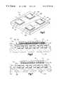
- FIG. 3illustrates an electronic package 60 embodying this invention, which substantially reduces bending or warpage from CTE differentials and the attendant risk of BGA and/or chip failure.
- Package 60includes a carrier 62 with a balancing layer 66 of thermotropic polymer, typically a few mils thick, sandwiched between an upper layer 64 and lower layer 68 , both of which are conventional glass-filled epoxy, polyimides or the like.
- thermotropic polymersinclude the liquid crystalline polyesters described in U.S. Pat. No. 4,818,812 to Economy et al. (the disclosure of which is incorporated by reference). These polymers contain about 25 to about 100 mole percent of recurring Unit I and O to about 75 mole percent of recurring Unit II wherein:
- each R and R 2individually, is an arylene group, a cycloalkylene group, aklylene group or mixture thereof.
- Especially preferred materialsinclude the polymer disclosed in Example 2 of the Economy et al patent, which is produced with about 35.66 parts by weight of 2-chloro 1,4 diacetoxybenzene, about 26.86 parts by weight of trans 1,4-cyclohexanedicarboxylic acid, and about 37.47 parts by weight of 4-acetoxy benzoic acid and the polymer disclosed in Example 4, which is produced with about 39.59 parts by weight of 1,4-diacetoxy-2-phenyl benzene, about 25.22 parts by weight of trans 1,4 cyclohexanedicarboxylic acid and about 35.19 parts by weight of 4-acetoxy benzoic acid.
- thermotropic liquid crystalline polyestersmay be readily processed to have CTEs of 5 to 20 ppm/° C. With certain materials and processing techniques, the CTE can be as low as about minus 5 ppm/° C., but that level of CTE adjustment is not normally required to achieve superior results with the methods and structures of this invention. If the thermotropic liquid crystalline polymer in layer 66 has a CTE of five ppm/° C. and makes up one-half of the overall thickness of substrate 61 , and the upper layer 64 and bottom layer 68 of the substrate are each made of glass filled epoxy having a CTE of 20 ppm/° C., together forming the remaining half of the thickness of carrier 62 , the average CTE of carrier 62 will be 12.5 ppm/° C. Thus, the differential between the CTE of chip 12 and substrate 62 has been effectively reduced by about 50%. This brings the strain on the C4 solder connections between the chip and carrier, and warping of the chip and carrier, within acceptable limits for many applications.
- FIG. 4illustrates another package 80 embodying this invention, in which carrier 82 has a layer 86 of thermotropic polymer, preferably of about the same thickness as the layer 66 of thermotropic polymer in FIG. 3, applied to the surface of a circuitized glass filled epoxy substrate 88 .
- Layer 86is applied to the surface of carrier 82 before chip 12 is attached.
- Contacts and other conventional circuitryare applied to the top of thermotropic layer 86 , the chip is attached to these contacts, and underfill layer 48 is applied and cured by conventional methods.
- thermotropic layers up or down in carriers and other substrates as illustrated, for example, in FIGS. 3 and 4enables us to control CTE mismatch at particular locations. Therefore, there should be a careful selection of a proper cross-section within the package to get optimal mechanical performance.
- FIG. 5shows a package 100 with four chips 12 are attached to a circuitized organic dielectric multichip carrier 102 with C4 connections (not shown). Each chip 12 is separated from the carrier 102 by an individual patch 106 of thermotropic polymer and an individual patch 48 of underfill. This makes it possible to tailor CTE balancing to different chips in a common package. Four chips are illustrated, but carriers may hold a. multiplicity of chips and devices depending on the application.
- FIGS. 6illustrates another embodiment in which coefficients of thermal expansion are adjusted to achieve particularly desired levels at different points in a carrier 120 .
- the illustrated multi-layered carrier 120has a layer 126 of a thermotropic polymer having a CTE of about 3 pm on the side of the carrier nearest to the chip 12 , which also has a CTE of about 3 ppm/° C. This layer should be a few mils thick.
- a layer 128 of glass-filled epoxy or other conventional organic dielectric (also be a few mils thick) having a CTE of about 20 ppm/° C.forms the bottom of carrier 122 , nearest to the printed circuit board 32 to which it is attached, which also has a CTE of about 20 ppm/° C.
- Elastic layer 132which may also be a few mils thick, effectively decouples the balancing layer and the lower layer, and absorbs shear strains without undue warping of the carrier 122 or chip 12 .
- FIG. 7illustrates yet another embodiment of this invention in which a layer 166 of thermotropic polymer reduces the overall co-efficient of thermal expansion of a multi-layered substrate.
- the multi-layer substrateis a printed circuit board or card 162 , having an upper layer 164 and lower layer 168 , both of which comprise a glass filled epoxy, polyimide or other conventional organic dielectric material, with a layer 166 of a thermotropic polymer such as the liquid crystalline polyesters discussed above between upper layer 164 and lower layer 168 .
- An integrated circuit chip 12is connected by C4 connections 16 to a ceramic chip carrier 152 , which has a coefficient of thermal expansion of about 8-10 ppm/° C.
- the ceramic chip carrier 152is connected by an array of solder balls 28 to contacts 34 on the upper surface of printed circuit board or cord 162 . If the entire printed circuit board or card were made of a typical circuitized organic dielectric material with a CTE of about 15-25 ppm/° C., the differences between the thermal expansion of the ceramic carrier 152 , and the co-efficient of thermal expansion of the printed circuit board or card 162 would produce shearing stresses and strains on the BGA solder balls 28 that would be undesirable and perhaps unacceptable. However, in the structure illustrated in FIG.
- the balancing layer 166 of thermotropic polymerwhich may be about 10 to 20 and is preferably about 15 mils thick and preferably has a CTE of about 5 ppm/° C.
- This layermay form about 40 to 60% of the thickness of the printed circuit board or card, and reduces the overall or average coefficient of thermal expansion of the board to about 12 ppm/° C. This reduces shearing stresses and strains on the BGA solder balls 28 significantly and brings them within acceptable levels.
- this inventionprovides an effective, practical and cost effective method for reducing warping in packages with flip-chip attachments to circuitized organic dielectric substrates. These improvements are achieved without creating the alternative problems that plagued prior approaches to this problem.
- those skilled in the artwill also appreciate that many modifications may be made to the materials, structures and methods disclosed above within the scope of this invention, which is defined by the following claims.
Landscapes
- Engineering & Computer Science (AREA)
- Power Engineering (AREA)
- Computer Hardware Design (AREA)
- Microelectronics & Electronic Packaging (AREA)
- General Physics & Mathematics (AREA)
- Condensed Matter Physics & Semiconductors (AREA)
- Physics & Mathematics (AREA)
- Chemical & Material Sciences (AREA)
- Materials Engineering (AREA)
- Manufacturing & Machinery (AREA)
- Wire Bonding (AREA)
- Laminated Bodies (AREA)
- Structures For Mounting Electric Components On Printed Circuit Boards (AREA)
Abstract
Description


Claims (16)


Priority Applications (4)
| Application Number | Priority Date | Filing Date | Title |
|---|---|---|---|
| US09/067,707US6177728B1 (en) | 1998-04-28 | 1998-04-28 | Integrated circuit chip device having balanced thermal expansion |
| TW088103858ATW424285B (en) | 1998-04-28 | 1999-03-12 | Methods and apparatus for balancing differences in thermal expansion in electronic packaging |
| KR1019990010906AKR100339178B1 (en) | 1998-04-28 | 1999-03-30 | Methods and apparatus for balancing differences in thermal expansion in electronic packaging |
| US09/643,522US6569711B1 (en) | 1998-04-28 | 2000-08-22 | Methods and apparatus for balancing differences in thermal expansion in electronic packaging |
Applications Claiming Priority (1)
| Application Number | Priority Date | Filing Date | Title |
|---|---|---|---|
| US09/067,707US6177728B1 (en) | 1998-04-28 | 1998-04-28 | Integrated circuit chip device having balanced thermal expansion |
Related Child Applications (1)
| Application Number | Title | Priority Date | Filing Date |
|---|---|---|---|
| US09/643,522DivisionUS6569711B1 (en) | 1998-04-28 | 2000-08-22 | Methods and apparatus for balancing differences in thermal expansion in electronic packaging |
Publications (1)
| Publication Number | Publication Date |
|---|---|
| US6177728B1true US6177728B1 (en) | 2001-01-23 |
Family
ID=22077833
Family Applications (2)
| Application Number | Title | Priority Date | Filing Date |
|---|---|---|---|
| US09/067,707Expired - LifetimeUS6177728B1 (en) | 1998-04-28 | 1998-04-28 | Integrated circuit chip device having balanced thermal expansion |
| US09/643,522Expired - Fee RelatedUS6569711B1 (en) | 1998-04-28 | 2000-08-22 | Methods and apparatus for balancing differences in thermal expansion in electronic packaging |
Family Applications After (1)
| Application Number | Title | Priority Date | Filing Date |
|---|---|---|---|
| US09/643,522Expired - Fee RelatedUS6569711B1 (en) | 1998-04-28 | 2000-08-22 | Methods and apparatus for balancing differences in thermal expansion in electronic packaging |
Country Status (3)
| Country | Link |
|---|---|
| US (2) | US6177728B1 (en) |
| KR (1) | KR100339178B1 (en) |
| TW (1) | TW424285B (en) |
Cited By (21)
| Publication number | Priority date | Publication date | Assignee | Title |
|---|---|---|---|---|
| US6320136B1 (en)* | 1999-01-25 | 2001-11-20 | Oki Electric Industry Co., Ltd. | Layered printed-circuit-board and module using the same |
| US6362437B1 (en)* | 1999-06-17 | 2002-03-26 | Nec Corporation | Mounting structure of integrated circuit device having high effect of buffering stress and high reliability of connection by solder, and method of mounting the same |
| US6399896B1 (en)* | 2000-03-15 | 2002-06-04 | International Business Machines Corporation | Circuit package having low modulus, conformal mounting pads |
| US20030141104A1 (en)* | 2000-02-23 | 2003-07-31 | Heinrich Bruckmann | Electronic printed-circuit board for electronic devices, especially communications terminals |
| US20030170444A1 (en)* | 2002-03-05 | 2003-09-11 | Stewart Steven L. | Attachment of surface mount devices to printed circuit boards using a thermoplastic adhesive |
| US20030170450A1 (en)* | 2002-03-05 | 2003-09-11 | Stewart Steven L. | Attachment of surface mount devices to printed circuit boards using a thermoplastic adhesive |
| US6697261B2 (en)* | 1998-07-01 | 2004-02-24 | Fujitsu Limited | Multileveled printed circuit board unit including substrate interposed between stacked bumps |
| US20040099958A1 (en)* | 2002-11-21 | 2004-05-27 | Schildgen William R. | Crack resistant interconnect module |
| WO2004027862A3 (en)* | 2002-09-19 | 2004-06-03 | Optitune Plc | Substrate based component packaging and assembly |
| US6816385B1 (en)* | 2000-11-16 | 2004-11-09 | International Business Machines Corporation | Compliant laminate connector |
| US20060060636A1 (en)* | 2004-09-22 | 2006-03-23 | International Business Machines Corporation | Solder interconnection array with optimal mechanical integrity |
| US20070111375A1 (en)* | 2005-11-15 | 2007-05-17 | Manepalli Rahul N | Enhancing shock resistance in semiconductor packages |
| US7253504B1 (en) | 2004-12-13 | 2007-08-07 | Advanced Micro Devices, Inc. | Integrated circuit package and method |
| US20080150132A1 (en)* | 2006-12-21 | 2008-06-26 | Tom Hu | Stack up pcb substrate for high density interconnect packages |
| US7432596B1 (en)* | 2004-10-12 | 2008-10-07 | Energy Innovations, Inc. | Apparatus and method for bonding silicon wafer to conductive substrate |
| US20080257586A1 (en)* | 2007-04-18 | 2008-10-23 | Industrial Technology Research Institute | Flexible circuit structure with stretchability and method of manufacturing the same |
| US20130299995A1 (en)* | 2012-05-08 | 2013-11-14 | Stats Chippac, Ltd. | Semiconductor Device and Method of Depositing Underfill Material With Uniform Flow Rate |
| CN105518858A (en)* | 2014-12-22 | 2016-04-20 | 英特尔公司 | Multilayer substrate for semiconductor package |
| US20170216947A1 (en)* | 2014-07-28 | 2017-08-03 | Xin Yang | Systems and methods for reinforced adhesive bonding |
| CN108695175A (en)* | 2017-04-07 | 2018-10-23 | 台湾积体电路制造股份有限公司 | Method for manufacturing semiconductor structure |
| US11304290B2 (en) | 2017-04-07 | 2022-04-12 | Taiwan Semiconductor Manufacturing Company, Ltd. | Semiconductor structures and methods |
Families Citing this family (21)
| Publication number | Priority date | Publication date | Assignee | Title |
|---|---|---|---|---|
| US8084866B2 (en) | 2003-12-10 | 2011-12-27 | Micron Technology, Inc. | Microelectronic devices and methods for filling vias in microelectronic devices |
| US7091124B2 (en) | 2003-11-13 | 2006-08-15 | Micron Technology, Inc. | Methods for forming vias in microelectronic devices, and methods for packaging microelectronic devices |
| US20050247894A1 (en) | 2004-05-05 | 2005-11-10 | Watkins Charles M | Systems and methods for forming apertures in microfeature workpieces |
| KR100630684B1 (en)* | 2004-06-08 | 2006-10-02 | 삼성전자주식회사 | Printed circuit board and semiconductor package module using the same to improve solder joint reliability |
| US7232754B2 (en) | 2004-06-29 | 2007-06-19 | Micron Technology, Inc. | Microelectronic devices and methods for forming interconnects in microelectronic devices |
| US7425499B2 (en) | 2004-08-24 | 2008-09-16 | Micron Technology, Inc. | Methods for forming interconnects in vias and microelectronic workpieces including such interconnects |
| SG120200A1 (en)* | 2004-08-27 | 2006-03-28 | Micron Technology Inc | Slanted vias for electrical circuits on circuit boards and other substrates |
| US7300857B2 (en) | 2004-09-02 | 2007-11-27 | Micron Technology, Inc. | Through-wafer interconnects for photoimager and memory wafers |
| US7105920B2 (en)* | 2004-11-12 | 2006-09-12 | Taiwan Semiconductor Manufacturing Company, Ltd. | Substrate design to improve chip package reliability |
| US7271482B2 (en) | 2004-12-30 | 2007-09-18 | Micron Technology, Inc. | Methods for forming interconnects in microelectronic workpieces and microelectronic workpieces formed using such methods |
| US7795134B2 (en) | 2005-06-28 | 2010-09-14 | Micron Technology, Inc. | Conductive interconnect structures and formation methods using supercritical fluids |
| US7262134B2 (en) | 2005-09-01 | 2007-08-28 | Micron Technology, Inc. | Microfeature workpieces and methods for forming interconnects in microfeature workpieces |
| US7622377B2 (en) | 2005-09-01 | 2009-11-24 | Micron Technology, Inc. | Microfeature workpiece substrates having through-substrate vias, and associated methods of formation |
| US7863187B2 (en) | 2005-09-01 | 2011-01-04 | Micron Technology, Inc. | Microfeature workpieces and methods for forming interconnects in microfeature workpieces |
| US7749899B2 (en) | 2006-06-01 | 2010-07-06 | Micron Technology, Inc. | Microelectronic workpieces and methods and systems for forming interconnects in microelectronic workpieces |
| US7629249B2 (en)* | 2006-08-28 | 2009-12-08 | Micron Technology, Inc. | Microfeature workpieces having conductive interconnect structures formed by chemically reactive processes, and associated systems and methods |
| US7902643B2 (en) | 2006-08-31 | 2011-03-08 | Micron Technology, Inc. | Microfeature workpieces having interconnects and conductive backplanes, and associated systems and methods |
| SG150410A1 (en) | 2007-08-31 | 2009-03-30 | Micron Technology Inc | Partitioned through-layer via and associated systems and methods |
| US7884015B2 (en)* | 2007-12-06 | 2011-02-08 | Micron Technology, Inc. | Methods for forming interconnects in microelectronic workpieces and microelectronic workpieces formed using such methods |
| KR100968278B1 (en)* | 2008-03-28 | 2010-07-06 | 삼성전기주식회사 | Insulation sheet, its manufacturing method and printed circuit board and its manufacturing method |
| US7863106B2 (en)* | 2008-12-24 | 2011-01-04 | International Business Machines Corporation | Silicon interposer testing for three dimensional chip stack |
Citations (22)
| Publication number | Priority date | Publication date | Assignee | Title |
|---|---|---|---|---|
| US4658332A (en) | 1983-04-04 | 1987-04-14 | Raytheon Company | Compliant layer printed circuit board |
| US4740414A (en) | 1986-11-17 | 1988-04-26 | Rockwell International Corporation | Ceramic/organic multilayer interconnection board |
| US4847146A (en) | 1988-03-21 | 1989-07-11 | Hughes Aircraft Company | Process for fabricating compliant layer board with selectively isolated solder pads |
| US4873615A (en) | 1986-10-09 | 1989-10-10 | Amp Incorporated | Semiconductor chip carrier system |
| US5026624A (en) | 1989-03-03 | 1991-06-25 | International Business Machines Corporation | Composition for photo imaging |
| US5049981A (en)* | 1990-10-19 | 1991-09-17 | At&T Bell Laboratories | Heat sink for electronic circitry |
| US5258648A (en) | 1991-06-27 | 1993-11-02 | Motorola, Inc. | Composite flip chip semiconductor device with an interposer having test contacts formed along its periphery |
| US5262280A (en) | 1992-04-02 | 1993-11-16 | Shipley Company Inc. | Radiation sensitive compositions |
| US5278010A (en) | 1989-03-03 | 1994-01-11 | International Business Machines Corporation | Composition for photo imaging |
| US5304457A (en) | 1989-03-03 | 1994-04-19 | International Business Machines Corporation | Composition for photo imaging |
| US5347162A (en)* | 1989-08-28 | 1994-09-13 | Lsi Logic Corporation | Preformed planar structures employing embedded conductors |
| US5371404A (en)* | 1993-02-04 | 1994-12-06 | Motorola, Inc. | Thermally conductive integrated circuit package with radio frequency shielding |
| US5439766A (en) | 1988-12-30 | 1995-08-08 | International Business Machines Corporation | Composition for photo imaging |
| US5439779A (en) | 1993-02-22 | 1995-08-08 | International Business Machines Corporation | Aqueous soldermask |
| US5473119A (en) | 1993-02-05 | 1995-12-05 | W. L. Gore & Associates, Inc. | Stress-resistant circuit board |
| US5473814A (en)* | 1994-01-07 | 1995-12-12 | International Business Machines Corporation | Process for surface mounting flip chip carrier modules |
| US5493075A (en) | 1994-09-30 | 1996-02-20 | International Business Machines Corporation | Fine pitch solder formation on printed circuit board process and product |
| US5496769A (en) | 1993-04-30 | 1996-03-05 | Commissariat A L'energie Atomique | Process for coating electronic components hybridized by bumps on a substrate |
| US5511306A (en) | 1994-04-05 | 1996-04-30 | Compaq Computer Corporation | Masking of circuit board vias to reduce heat-induced board and chip carrier package warp during wavesolder process |
| US5535101A (en) | 1992-11-03 | 1996-07-09 | Motorola, Inc. | Leadless integrated circuit package |
| US5579573A (en) | 1994-10-11 | 1996-12-03 | Ford Motor Company | Method for fabricating an undercoated chip electrically interconnected to a substrate |
| US5633535A (en) | 1995-01-27 | 1997-05-27 | Chao; Clinton C. | Spacing control in electronic device assemblies |
Family Cites Families (2)
| Publication number | Priority date | Publication date | Assignee | Title |
|---|---|---|---|---|
| JPH06291165A (en)* | 1993-04-01 | 1994-10-18 | Nec Corp | Flip chip connecting construction |
| JPH088511A (en)* | 1994-06-22 | 1996-01-12 | Oki Electric Ind Co Ltd | Bga package and manufacture thereof |
- 1998
- 1998-04-28USUS09/067,707patent/US6177728B1/ennot_activeExpired - Lifetime
- 1999
- 1999-03-12TWTW088103858Apatent/TW424285B/ennot_activeIP Right Cessation
- 1999-03-30KRKR1019990010906Apatent/KR100339178B1/ennot_activeExpired - Fee Related
- 2000
- 2000-08-22USUS09/643,522patent/US6569711B1/ennot_activeExpired - Fee Related
Patent Citations (22)
| Publication number | Priority date | Publication date | Assignee | Title |
|---|---|---|---|---|
| US4658332A (en) | 1983-04-04 | 1987-04-14 | Raytheon Company | Compliant layer printed circuit board |
| US4873615A (en) | 1986-10-09 | 1989-10-10 | Amp Incorporated | Semiconductor chip carrier system |
| US4740414A (en) | 1986-11-17 | 1988-04-26 | Rockwell International Corporation | Ceramic/organic multilayer interconnection board |
| US4847146A (en) | 1988-03-21 | 1989-07-11 | Hughes Aircraft Company | Process for fabricating compliant layer board with selectively isolated solder pads |
| US5439766A (en) | 1988-12-30 | 1995-08-08 | International Business Machines Corporation | Composition for photo imaging |
| US5304457A (en) | 1989-03-03 | 1994-04-19 | International Business Machines Corporation | Composition for photo imaging |
| US5026624A (en) | 1989-03-03 | 1991-06-25 | International Business Machines Corporation | Composition for photo imaging |
| US5278010A (en) | 1989-03-03 | 1994-01-11 | International Business Machines Corporation | Composition for photo imaging |
| US5347162A (en)* | 1989-08-28 | 1994-09-13 | Lsi Logic Corporation | Preformed planar structures employing embedded conductors |
| US5049981A (en)* | 1990-10-19 | 1991-09-17 | At&T Bell Laboratories | Heat sink for electronic circitry |
| US5258648A (en) | 1991-06-27 | 1993-11-02 | Motorola, Inc. | Composite flip chip semiconductor device with an interposer having test contacts formed along its periphery |
| US5262280A (en) | 1992-04-02 | 1993-11-16 | Shipley Company Inc. | Radiation sensitive compositions |
| US5535101A (en) | 1992-11-03 | 1996-07-09 | Motorola, Inc. | Leadless integrated circuit package |
| US5371404A (en)* | 1993-02-04 | 1994-12-06 | Motorola, Inc. | Thermally conductive integrated circuit package with radio frequency shielding |
| US5473119A (en) | 1993-02-05 | 1995-12-05 | W. L. Gore & Associates, Inc. | Stress-resistant circuit board |
| US5439779A (en) | 1993-02-22 | 1995-08-08 | International Business Machines Corporation | Aqueous soldermask |
| US5496769A (en) | 1993-04-30 | 1996-03-05 | Commissariat A L'energie Atomique | Process for coating electronic components hybridized by bumps on a substrate |
| US5473814A (en)* | 1994-01-07 | 1995-12-12 | International Business Machines Corporation | Process for surface mounting flip chip carrier modules |
| US5511306A (en) | 1994-04-05 | 1996-04-30 | Compaq Computer Corporation | Masking of circuit board vias to reduce heat-induced board and chip carrier package warp during wavesolder process |
| US5493075A (en) | 1994-09-30 | 1996-02-20 | International Business Machines Corporation | Fine pitch solder formation on printed circuit board process and product |
| US5579573A (en) | 1994-10-11 | 1996-12-03 | Ford Motor Company | Method for fabricating an undercoated chip electrically interconnected to a substrate |
| US5633535A (en) | 1995-01-27 | 1997-05-27 | Chao; Clinton C. | Spacing control in electronic device assemblies |
Non-Patent Citations (3)
| Title |
|---|
| 09/067,708; filed Apr. 28, 1998; inventor Jimarez et al. for Methods and Apparatus for Balancing Differences in Thermal Expansion in Electric Packaging. |
| 09/080,117; field May 15, 1998; inventor Caletka et al.. for Thermally Enhanced and Mechanically Balanced Flip Chip Package and Method of Forming. |
| IBM Technical Disclosure Bulletin, pp. 85-86, vol. 40 No. 04, Apr. 1997. |
Cited By (41)
| Publication number | Priority date | Publication date | Assignee | Title |
|---|---|---|---|---|
| US20040169277A1 (en)* | 1998-07-01 | 2004-09-02 | Fujitsu Limted | Multileveled printed circuit board unit including substrate interposed between stacked bumps |
| US7489518B2 (en) | 1998-07-01 | 2009-02-10 | Fujitsu Limited | Multileveled printed circuit board unit including substrate interposed between stacked bumps |
| US20090178835A1 (en)* | 1998-07-01 | 2009-07-16 | Fujitsu Limited | Multileveled printed circuit board unit including substrate interposed between stacked bumps |
| US6697261B2 (en)* | 1998-07-01 | 2004-02-24 | Fujitsu Limited | Multileveled printed circuit board unit including substrate interposed between stacked bumps |
| US8089775B2 (en) | 1998-07-01 | 2012-01-03 | Fujitsu Limited | Multileveled printed circuit board unit including substrate interposed between stacked bumps |
| US6320136B1 (en)* | 1999-01-25 | 2001-11-20 | Oki Electric Industry Co., Ltd. | Layered printed-circuit-board and module using the same |
| US6362437B1 (en)* | 1999-06-17 | 2002-03-26 | Nec Corporation | Mounting structure of integrated circuit device having high effect of buffering stress and high reliability of connection by solder, and method of mounting the same |
| US20030141104A1 (en)* | 2000-02-23 | 2003-07-31 | Heinrich Bruckmann | Electronic printed-circuit board for electronic devices, especially communications terminals |
| US6399896B1 (en)* | 2000-03-15 | 2002-06-04 | International Business Machines Corporation | Circuit package having low modulus, conformal mounting pads |
| US6816385B1 (en)* | 2000-11-16 | 2004-11-09 | International Business Machines Corporation | Compliant laminate connector |
| US6906425B2 (en) | 2002-03-05 | 2005-06-14 | Resolution Performance Products Llc | Attachment of surface mount devices to printed circuit boards using a thermoplastic adhesive |
| US20030170450A1 (en)* | 2002-03-05 | 2003-09-11 | Stewart Steven L. | Attachment of surface mount devices to printed circuit boards using a thermoplastic adhesive |
| US20030170444A1 (en)* | 2002-03-05 | 2003-09-11 | Stewart Steven L. | Attachment of surface mount devices to printed circuit boards using a thermoplastic adhesive |
| WO2004027862A3 (en)* | 2002-09-19 | 2004-06-03 | Optitune Plc | Substrate based component packaging and assembly |
| US8531045B2 (en) | 2002-09-19 | 2013-09-10 | Optitune Public Limited Company | Component packaging and assembly |
| US20060151859A1 (en)* | 2002-09-19 | 2006-07-13 | Ari Karkkainen | Component packaging and assembly |
| US20040099958A1 (en)* | 2002-11-21 | 2004-05-27 | Schildgen William R. | Crack resistant interconnect module |
| WO2004049437A1 (en)* | 2002-11-21 | 2004-06-10 | 3M Innovative Properties Company | Crack resistant interconnect module |
| US20080261350A1 (en)* | 2004-09-22 | 2008-10-23 | International Business Machines Corporation | Solder interconnection array with optimal mechanical integrity |
| US7445141B2 (en) | 2004-09-22 | 2008-11-04 | International Business Machines Corporation | Solder interconnection array with optimal mechanical integrity |
| US20060060636A1 (en)* | 2004-09-22 | 2006-03-23 | International Business Machines Corporation | Solder interconnection array with optimal mechanical integrity |
| US7900809B2 (en) | 2004-09-22 | 2011-03-08 | International Business Machines Corporation | Solder interconnection array with optimal mechanical integrity |
| US7432596B1 (en)* | 2004-10-12 | 2008-10-07 | Energy Innovations, Inc. | Apparatus and method for bonding silicon wafer to conductive substrate |
| US7253504B1 (en) | 2004-12-13 | 2007-08-07 | Advanced Micro Devices, Inc. | Integrated circuit package and method |
| US20070111375A1 (en)* | 2005-11-15 | 2007-05-17 | Manepalli Rahul N | Enhancing shock resistance in semiconductor packages |
| US7718904B2 (en)* | 2005-11-15 | 2010-05-18 | Intel Corporation | Enhancing shock resistance in semiconductor packages |
| TWI387061B (en)* | 2005-11-15 | 2013-02-21 | Intel Corp | Semiconductor package seismic enhancement technology |
| US20080150132A1 (en)* | 2006-12-21 | 2008-06-26 | Tom Hu | Stack up pcb substrate for high density interconnect packages |
| US20080257586A1 (en)* | 2007-04-18 | 2008-10-23 | Industrial Technology Research Institute | Flexible circuit structure with stretchability and method of manufacturing the same |
| US8513532B2 (en) | 2007-04-18 | 2013-08-20 | Industrial Technology Research Institute | Flexible circuit structure with stretchability and method of manufacturing the same |
| US20130299995A1 (en)* | 2012-05-08 | 2013-11-14 | Stats Chippac, Ltd. | Semiconductor Device and Method of Depositing Underfill Material With Uniform Flow Rate |
| US9390945B2 (en)* | 2012-05-08 | 2016-07-12 | STATS ChipPAC Pte. Ltd. | Semiconductor device and method of depositing underfill material with uniform flow rate |
| US20170216947A1 (en)* | 2014-07-28 | 2017-08-03 | Xin Yang | Systems and methods for reinforced adhesive bonding |
| CN105518858A (en)* | 2014-12-22 | 2016-04-20 | 英特尔公司 | Multilayer substrate for semiconductor package |
| WO2016105349A1 (en)* | 2014-12-22 | 2016-06-30 | Intel Corporation | Multilayer substrate for semiconductor packaging |
| US9788416B2 (en) | 2014-12-22 | 2017-10-10 | Intel Corporation | Multilayer substrate for semiconductor packaging |
| TWI603437B (en)* | 2014-12-22 | 2017-10-21 | 英特爾公司 | Multilayer substrate for semiconductor packaging |
| CN105518858B (en)* | 2014-12-22 | 2019-02-22 | 英特尔公司 | MULTILAYER SUBSTRATE for semiconductor packages |
| CN108695175A (en)* | 2017-04-07 | 2018-10-23 | 台湾积体电路制造股份有限公司 | Method for manufacturing semiconductor structure |
| CN108695175B (en)* | 2017-04-07 | 2020-06-26 | 台湾积体电路制造股份有限公司 | Manufacturing method of semiconductor structure |
| US11304290B2 (en) | 2017-04-07 | 2022-04-12 | Taiwan Semiconductor Manufacturing Company, Ltd. | Semiconductor structures and methods |
Also Published As
| Publication number | Publication date |
|---|---|
| TW424285B (en) | 2001-03-01 |
| KR19990082780A (en) | 1999-11-25 |
| US6569711B1 (en) | 2003-05-27 |
| KR100339178B1 (en) | 2002-05-31 |
Similar Documents
| Publication | Publication Date | Title |
|---|---|---|
| US6177728B1 (en) | Integrated circuit chip device having balanced thermal expansion | |
| US6191952B1 (en) | Compliant surface layer for flip-chip electronic packages and method for forming same | |
| US6562662B2 (en) | Electronic package with bonded structure and method of making | |
| US7026706B2 (en) | Method and packaging structure for optimizing warpage of flip chip organic packages | |
| US6490161B1 (en) | Peripheral land grid array package with improved thermal performance | |
| US6410988B1 (en) | Thermally enhanced and mechanically balanced flip chip package and method of forming | |
| US6949415B2 (en) | Module with adhesively attached heat sink | |
| US6299053B1 (en) | Isolated flip chip or BGA to minimize interconnect stress due to thermal mismatch | |
| US6317331B1 (en) | Wiring substrate with thermal insert | |
| KR20000022978A (en) | Interposer for recessed flip-chip package | |
| US7300822B2 (en) | Low warpage flip chip package solution-channel heat spreader | |
| US7491624B2 (en) | Method of manufacturing low CTE substrates for use with low-k flip-chip package devices | |
| US7633142B2 (en) | Flexible core for enhancement of package interconnect reliability | |
| US7227268B2 (en) | Placement of sacrificial solder balls underneath the PBGA substrate | |
| US6956165B1 (en) | Underfill for maximum flip chip package reliability | |
| US7504718B2 (en) | Apparatus and methods for constructing balanced chip packages to reduce thermally induced mechanical strain | |
| KR20050075340A (en) | Crack resistant interconnect module | |
| EP1473977A2 (en) | Electronic package with strengthened conductive pad | |
| US6989607B2 (en) | Stress reduction in flip-chip PBGA packaging by utilizing segmented chips and/or chip carriers | |
| Itagaki et al. | Packaging properties of ALIVH-CSP using SBB flip-chip bonding technology | |
| JPH11121525A (en) | Semiconductor device | |
| US20060043602A1 (en) | Flip chip ball grid array package with constraint plate | |
| HK1023221A (en) | Compliant surface layer for flip-chip electronic packages and method for forming same |
Legal Events
| Date | Code | Title | Description |
|---|---|---|---|
| AS | Assignment | Owner name:INTERNATIONAL BUSINESS MACHINES CORPORATION, NEW Y Free format text:ASSIGNMENT OF ASSIGNORS INTEREST;ASSIGNORS:SUSKO, ROBIN A.;WILSON, JAMES W.;REEL/FRAME:010902/0274;SIGNING DATES FROM 19981117 TO 19981204 | |
| FEPP | Fee payment procedure | Free format text:PAYOR NUMBER ASSIGNED (ORIGINAL EVENT CODE: ASPN); ENTITY STATUS OF PATENT OWNER: LARGE ENTITY | |
| STCF | Information on status: patent grant | Free format text:PATENTED CASE | |
| FPAY | Fee payment | Year of fee payment:4 | |
| FPAY | Fee payment | Year of fee payment:8 | |
| REMI | Maintenance fee reminder mailed | ||
| FPAY | Fee payment | Year of fee payment:12 | |
| SULP | Surcharge for late payment | Year of fee payment:11 | |
| AS | Assignment | Owner name:GLOBALFOUNDRIES U.S. 2 LLC, NEW YORK Free format text:ASSIGNMENT OF ASSIGNORS INTEREST;ASSIGNOR:INTERNATIONAL BUSINESS MACHINES CORPORATION;REEL/FRAME:036550/0001 Effective date:20150629 | |
| AS | Assignment | Owner name:GLOBALFOUNDRIES INC., CAYMAN ISLANDS Free format text:ASSIGNMENT OF ASSIGNORS INTEREST;ASSIGNORS:GLOBALFOUNDRIES U.S. 2 LLC;GLOBALFOUNDRIES U.S. INC.;REEL/FRAME:036779/0001 Effective date:20150910 | |
| AS | Assignment | Owner name:GLOBALFOUNDRIES U.S. INC., NEW YORK Free format text:RELEASE BY SECURED PARTY;ASSIGNOR:WILMINGTON TRUST, NATIONAL ASSOCIATION;REEL/FRAME:056987/0001 Effective date:20201117 |