US6177353B1 - Metallization etching techniques for reducing post-etch corrosion of metal lines - Google Patents
Metallization etching techniques for reducing post-etch corrosion of metal linesDownload PDFInfo
- Publication number
- US6177353B1 US6177353B1US09/153,390US15339098AUS6177353B1US 6177353 B1US6177353 B1US 6177353B1US 15339098 AUS15339098 AUS 15339098AUS 6177353 B1US6177353 B1US 6177353B1
- Authority
- US
- United States
- Prior art keywords
- hard mask
- layer
- etch
- metallization
- photoresist
- Prior art date
- Legal status (The legal status is an assumption and is not a legal conclusion. Google has not performed a legal analysis and makes no representation as to the accuracy of the status listed.)
- Expired - Lifetime
Links
- 229910052751metalInorganic materials0.000titleclaimsabstractdescription86
- 239000002184metalSubstances0.000titleclaimsabstractdescription86
- 238000000034methodMethods0.000titleclaimsabstractdescription72
- 238000001465metallisationMethods0.000titleclaimsabstractdescription65
- 238000005530etchingMethods0.000titleclaimsdescription38
- 238000005260corrosionMethods0.000titleclaimsdescription13
- 230000007797corrosionEffects0.000titleclaimsdescription13
- 229920002120photoresistant polymerPolymers0.000claimsabstractdescription58
- 229920000642polymerPolymers0.000claimsabstractdescription35
- 239000000758substrateSubstances0.000claimsabstractdescription19
- 238000000151depositionMethods0.000claimsabstractdescription15
- 230000008021depositionEffects0.000claimsabstractdescription15
- 239000000126substanceSubstances0.000claimsabstractdescription8
- 229910052782aluminiumInorganic materials0.000claimsdescription17
- XAGFODPZIPBFFR-UHFFFAOYSA-NaluminiumChemical compound[Al]XAGFODPZIPBFFR-UHFFFAOYSA-N0.000claimsdescription16
- 239000000463materialSubstances0.000claimsdescription13
- 238000002161passivationMethods0.000claimsdescription12
- 239000003795chemical substances by applicationSubstances0.000claimsdescription10
- 238000001020plasma etchingMethods0.000claimsdescription7
- VYPSYNLAJGMNEJ-UHFFFAOYSA-NSilicium dioxideChemical compoundO=[Si]=OVYPSYNLAJGMNEJ-UHFFFAOYSA-N0.000claimsdescription6
- 229910052814silicon oxideInorganic materials0.000claimsdescription5
- XPDWGBQVDMORPB-UHFFFAOYSA-NFluoroformChemical compoundFC(F)FXPDWGBQVDMORPB-UHFFFAOYSA-N0.000claimsdescription4
- 229910052681coesiteInorganic materials0.000claimsdescription3
- 229910052906cristobaliteInorganic materials0.000claimsdescription3
- 230000003628erosive effectEffects0.000claimsdescription3
- 239000000377silicon dioxideSubstances0.000claimsdescription3
- 229910052682stishoviteInorganic materials0.000claimsdescription3
- 229910052905tridymiteInorganic materials0.000claimsdescription3
- ATJFFYVFTNAWJD-UHFFFAOYSA-NTinChemical compound[Sn]ATJFFYVFTNAWJD-UHFFFAOYSA-N0.000claimsdescription2
- 239000000203mixtureSubstances0.000claimsdescription2
- 229910004541SiNInorganic materials0.000claims1
- 239000010410layerSubstances0.000description108
- KZBUYRJDOAKODT-UHFFFAOYSA-NChlorineChemical compoundClClKZBUYRJDOAKODT-UHFFFAOYSA-N0.000description17
- 230000004888barrier functionEffects0.000description16
- 239000006117anti-reflective coatingSubstances0.000description15
- 239000007789gasSubstances0.000description10
- 229910015844BCl3Inorganic materials0.000description8
- FAQYAMRNWDIXMY-UHFFFAOYSA-NtrichloroboraneChemical compoundClB(Cl)ClFAQYAMRNWDIXMY-UHFFFAOYSA-N0.000description8
- 239000010936titaniumSubstances0.000description6
- ZAMOUSCENKQFHK-UHFFFAOYSA-NChlorine atomChemical compound[Cl]ZAMOUSCENKQFHK-UHFFFAOYSA-N0.000description5
- 239000000460chlorineSubstances0.000description5
- 229910052801chlorineInorganic materials0.000description5
- XLYOFNOQVPJJNP-UHFFFAOYSA-NwaterChemical compoundOXLYOFNOQVPJJNP-UHFFFAOYSA-N0.000description5
- RTAQQCXQSZGOHL-UHFFFAOYSA-NTitaniumChemical compound[Ti]RTAQQCXQSZGOHL-UHFFFAOYSA-N0.000description4
- 239000010949copperSubstances0.000description4
- 229910052719titaniumInorganic materials0.000description4
- 229910001868waterInorganic materials0.000description4
- NRTOMJZYCJJWKI-UHFFFAOYSA-NTitanium nitrideChemical compound[Ti]#NNRTOMJZYCJJWKI-UHFFFAOYSA-N0.000description3
- 238000004380ashingMethods0.000description3
- 229910052802copperInorganic materials0.000description3
- XKRFYHLGVUSROY-UHFFFAOYSA-NArgonChemical compound[Ar]XKRFYHLGVUSROY-UHFFFAOYSA-N0.000description2
- OKTJSMMVPCPJKN-UHFFFAOYSA-NCarbonChemical compound[C]OKTJSMMVPCPJKN-UHFFFAOYSA-N0.000description2
- RYGMFSIKBFXOCR-UHFFFAOYSA-NCopperChemical compound[Cu]RYGMFSIKBFXOCR-UHFFFAOYSA-N0.000description2
- 230000004075alterationEffects0.000description2
- 229910052799carbonInorganic materials0.000description2
- 239000012634fragmentSubstances0.000description2
- 238000004519manufacturing processMethods0.000description2
- 150000002739metalsChemical class0.000description2
- 238000001039wet etchingMethods0.000description2
- 229910000838Al alloyInorganic materials0.000description1
- 239000002253acidSubstances0.000description1
- 150000007513acidsChemical class0.000description1
- 230000002411adverseEffects0.000description1
- 229910045601alloyInorganic materials0.000description1
- 239000000956alloySubstances0.000description1
- -1and the like)Substances0.000description1
- 229910052786argonInorganic materials0.000description1
- 230000015572biosynthetic processEffects0.000description1
- 239000006227byproductSubstances0.000description1
- 239000011248coating agentSubstances0.000description1
- 238000000576coating methodMethods0.000description1
- 239000002131composite materialSubstances0.000description1
- 150000001875compoundsChemical class0.000description1
- 238000000276deep-ultraviolet lithographyMethods0.000description1
- 239000008367deionised waterSubstances0.000description1
- 229910021641deionized waterInorganic materials0.000description1
- 239000003989dielectric materialSubstances0.000description1
- 238000003487electrochemical reactionMethods0.000description1
- 238000005868electrolysis reactionMethods0.000description1
- 230000008030eliminationEffects0.000description1
- 238000003379elimination reactionMethods0.000description1
- 239000011810insulating materialSubstances0.000description1
- 238000001459lithographyMethods0.000description1
- 239000011368organic materialSubstances0.000description1
- 239000003960organic solventSubstances0.000description1
- 150000002978peroxidesChemical class0.000description1
- 238000000206photolithographyMethods0.000description1
- 239000002243precursorSubstances0.000description1
- 239000000047productSubstances0.000description1
- 239000004065semiconductorSubstances0.000description1
- 229910052710siliconInorganic materials0.000description1
- 239000010703siliconSubstances0.000description1
- WFKWXMTUELFFGS-UHFFFAOYSA-NtungstenChemical compound[W]WFKWXMTUELFFGS-UHFFFAOYSA-N0.000description1
- 229910052721tungstenInorganic materials0.000description1
- 239000010937tungstenSubstances0.000description1
Images

Classifications
- C—CHEMISTRY; METALLURGY
- C23—COATING METALLIC MATERIAL; COATING MATERIAL WITH METALLIC MATERIAL; CHEMICAL SURFACE TREATMENT; DIFFUSION TREATMENT OF METALLIC MATERIAL; COATING BY VACUUM EVAPORATION, BY SPUTTERING, BY ION IMPLANTATION OR BY CHEMICAL VAPOUR DEPOSITION, IN GENERAL; INHIBITING CORROSION OF METALLIC MATERIAL OR INCRUSTATION IN GENERAL
- C23C—COATING METALLIC MATERIAL; COATING MATERIAL WITH METALLIC MATERIAL; SURFACE TREATMENT OF METALLIC MATERIAL BY DIFFUSION INTO THE SURFACE, BY CHEMICAL CONVERSION OR SUBSTITUTION; COATING BY VACUUM EVAPORATION, BY SPUTTERING, BY ION IMPLANTATION OR BY CHEMICAL VAPOUR DEPOSITION, IN GENERAL
- C23C16/00—Chemical coating by decomposition of gaseous compounds, without leaving reaction products of surface material in the coating, i.e. chemical vapour deposition [CVD] processes
- C23C16/06—Chemical coating by decomposition of gaseous compounds, without leaving reaction products of surface material in the coating, i.e. chemical vapour deposition [CVD] processes characterised by the deposition of metallic material
- C23C16/18—Chemical coating by decomposition of gaseous compounds, without leaving reaction products of surface material in the coating, i.e. chemical vapour deposition [CVD] processes characterised by the deposition of metallic material from metallo-organic compounds
- H—ELECTRICITY
- H01—ELECTRIC ELEMENTS
- H01L—SEMICONDUCTOR DEVICES NOT COVERED BY CLASS H10
- H01L21/00—Processes or apparatus adapted for the manufacture or treatment of semiconductor or solid state devices or of parts thereof
- H01L21/02—Manufacture or treatment of semiconductor devices or of parts thereof
- H01L21/02041—Cleaning
- H01L21/02057—Cleaning during device manufacture
- H01L21/02068—Cleaning during device manufacture during, before or after processing of conductive layers, e.g. polysilicon or amorphous silicon layers
- H01L21/02071—Cleaning during device manufacture during, before or after processing of conductive layers, e.g. polysilicon or amorphous silicon layers the processing being a delineation, e.g. RIE, of conductive layers
- H—ELECTRICITY
- H01—ELECTRIC ELEMENTS
- H01L—SEMICONDUCTOR DEVICES NOT COVERED BY CLASS H10
- H01L21/00—Processes or apparatus adapted for the manufacture or treatment of semiconductor or solid state devices or of parts thereof
- H01L21/02—Manufacture or treatment of semiconductor devices or of parts thereof
- H01L21/04—Manufacture or treatment of semiconductor devices or of parts thereof the devices having potential barriers, e.g. a PN junction, depletion layer or carrier concentration layer
- H01L21/18—Manufacture or treatment of semiconductor devices or of parts thereof the devices having potential barriers, e.g. a PN junction, depletion layer or carrier concentration layer the devices having semiconductor bodies comprising elements of Group IV of the Periodic Table or AIIIBV compounds with or without impurities, e.g. doping materials
- H01L21/30—Treatment of semiconductor bodies using processes or apparatus not provided for in groups H01L21/20 - H01L21/26
- H01L21/31—Treatment of semiconductor bodies using processes or apparatus not provided for in groups H01L21/20 - H01L21/26 to form insulating layers thereon, e.g. for masking or by using photolithographic techniques; After treatment of these layers; Selection of materials for these layers
- H01L21/3205—Deposition of non-insulating-, e.g. conductive- or resistive-, layers on insulating layers; After-treatment of these layers
- H01L21/321—After treatment
- H01L21/3213—Physical or chemical etching of the layers, e.g. to produce a patterned layer from a pre-deposited extensive layer
- H01L21/32133—Physical or chemical etching of the layers, e.g. to produce a patterned layer from a pre-deposited extensive layer by chemical means only
- H01L21/32135—Physical or chemical etching of the layers, e.g. to produce a patterned layer from a pre-deposited extensive layer by chemical means only by vapour etching only
- H01L21/32136—Physical or chemical etching of the layers, e.g. to produce a patterned layer from a pre-deposited extensive layer by chemical means only by vapour etching only using plasmas
- H—ELECTRICITY
- H01—ELECTRIC ELEMENTS
- H01L—SEMICONDUCTOR DEVICES NOT COVERED BY CLASS H10
- H01L21/00—Processes or apparatus adapted for the manufacture or treatment of semiconductor or solid state devices or of parts thereof
- H01L21/02—Manufacture or treatment of semiconductor devices or of parts thereof
- H01L21/04—Manufacture or treatment of semiconductor devices or of parts thereof the devices having potential barriers, e.g. a PN junction, depletion layer or carrier concentration layer
- H01L21/18—Manufacture or treatment of semiconductor devices or of parts thereof the devices having potential barriers, e.g. a PN junction, depletion layer or carrier concentration layer the devices having semiconductor bodies comprising elements of Group IV of the Periodic Table or AIIIBV compounds with or without impurities, e.g. doping materials
- H01L21/30—Treatment of semiconductor bodies using processes or apparatus not provided for in groups H01L21/20 - H01L21/26
- H01L21/31—Treatment of semiconductor bodies using processes or apparatus not provided for in groups H01L21/20 - H01L21/26 to form insulating layers thereon, e.g. for masking or by using photolithographic techniques; After treatment of these layers; Selection of materials for these layers
- H01L21/3205—Deposition of non-insulating-, e.g. conductive- or resistive-, layers on insulating layers; After-treatment of these layers
- H01L21/321—After treatment
- H01L21/3213—Physical or chemical etching of the layers, e.g. to produce a patterned layer from a pre-deposited extensive layer
- H01L21/32139—Physical or chemical etching of the layers, e.g. to produce a patterned layer from a pre-deposited extensive layer using masks
Definitions
- Metal layer 108is typically formed of aluminum or one of its alloys such as aluminum/copper or aluminum/copper/silicon. Between metal layer 108 and photoresist mask 110 , there is disposed a barrier/ARC (anti-reflective coating) layer 112 .
- Barrier/ARC layer 112may include, for example, an overlaying anti-reflective coating, which may be organic or inorganic in character.
- the anti-reflective coating layeris provided primarily for the lithography purposes.
- a barrier layer of titanium and/or titanium nitridemay be disposed under the aforementioned anti-reflective coating layer.
- metal layer 102is shown including barrier/ARC layer 112 , metal layer 108 , and barrier layer 106 , one skilled in the art would readily recognize that both barrier/ARC layer 112 and barrier layer 106 are optional and one or both may be omitted in some ICs.
- Photoresist mask 110represents a portion of the photoresist mask that has been formed using an appropriate photoresist process. During the etching of metal layer 102 , photoresist mask 110 protects the portions of the metal layer 102 disposed below the photoresist features, thereby forming features out of the underlying metal layer. By way of example, the etching of metal layer 102 produces a line disposed perpendicular to the page on which FIG. 1 is depicted.
- etchingis completed and portions of metal layer 102 that are not protected by the photoresist features are removed.
- the etching of an aluminum-containing metal layeris accomplished in a plasma reactor using, for example, etching source gases such as Cl 2 /BCl 3 , CL 2 /HCl, CL 2 /N 2 , and the like.
- the etchingmay be performed in accordance with a plasma-enhanced process known as reactive ion etching (RIE), for example.
- RIEreactive ion etching
- FIG. 2there are shown polymer side walls 202 A and 202 B coating the vertical surfaces of metal feature 204 .
- the polymer side wallscontain organic materials such as sputtered photoresist from photoresist mask 110 , resputtered material from the metallization layers (such as aluminum, titanium, and the like), material sputtered from the underlying layer (such as from substrate 104 ) and a nontrivial amount of chlorine and/or chlorine-containing compounds from the etching source gas.
- the polymer side wallsneed to be removed as part of the post metallization processing steps.
- the photoresist maskis removed.
- photoresist mask removalmay be achieved by stripping away the photoresist material in a downstream ash plasma reactor using, for example, O 2 /H 2 O vapor or O 2 as the ashing material.
- the photoresist strip processremoves very little, if any, of the side wall polymers. Consequently, the polymer side walls remain after the photoresist strip process and must be removed in a subsequent process step. Complete removal of the polymer side walls is highly desirable because if side wall polymer remains attached to the metal line, the chlorine therein may react with moisture in the ambient environment, forming corrosive acids that attack the metal lines.
- erosion of the metal lineschanges the electrical characteristics of metal lines, e.g., increasing their resistivity.
- the corrosionmay be severe enough to sever the conductive path, forming an open circuit where none is intended.
- the wet etch processaccomplishes its purpose of removing the polymer side wall, there are disadvantages.
- the wet etch processtypically employs corrosive chemicals that typically do not have a high selectivity to aluminum. If the wet etch process is not carefully controlled, the wet etchant can attack the aluminum lines especially at the interface with the upper and/or lower barrier layers or at the interface between an aluminum line and an underlying tungsten stud. The stud-related corrosion is particularly severe if there is any stud that is misaligned with the metal line (due to, e.g., manufacturing tolerance) and is therefore not completely covered by a metal line.
- the inventionrelates, in one embodiment, to a method for reducing polymer deposition on vertical surfaces of metal lines etched from a metallization layer disposed above a substrate.
- the methodincludes forming a hard mask layer above the metallization layer and providing a photoresist mask above the hard mask layer.
- the methodfurther includes employing the photoresist mask to form a hard mask from the hard mask layer.
- the hard maskhas patterns therein configured to form the metal lines in a subsequent plasma-enhanced metallization etch. There is also included removing the photoresist mask.
- the inventionin another embodiment, relates to a method for reducing corrosion of metal lines etched from a metallization layer that is disposed above a substrate.
- the methodincludes providing the substrate having thereon the metallization layer.
- the metallization layerincludes at least two layers having different electrochemical characteristics.
- the methodadditionally includes forming a hard mask layer above the metallization layer and providing a photoresist mask above the hard mask layer. Further, there is included employing the photoresist mask to form a hard mask from the hard mask layer.
- the hard maskhas patterns therein configured to form the metal lines in a subsequent plasma-enhanced metallization etch.
- the methodalso includes removing the photoresist mask and performing the plasma-enhanced metallization etch employing the hard mask and an etchant source gas that includes Cl2 and at least one passivation-forming chemical, wherein the plasma-enhanced metallization etch is performed without employing photoresist to reduce photoresist-based polymer deposition during the plasma-enhanced metallization etch.
- the methodadditionally includes performing a wet etch to remove polymer side walls formed during the plasma-enhanced metallization etch. The wet etch is performed while the hard mask is disposed above the metal lines to reduce the corrosion due to an electrolysis reaction between the at least two metal layers during the wet etch.
- FIG. 2depicts the substrate of FIG. 1 after the metallization layer is etched.
- FIG. 3depicts the substrate of FIG. 2 after the photoresist mask is removed.
- FIG. 4shows the metallization feature of FIG. 3 after the wet etch has been performed to remove the polymer side walls.
- FIG. 5depicts a metal layer disposed on a substrate, including a hard mask layer and a photoresist mask that are disposed above the metal layer to facilitate metallization etching.
- FIG. 6depicts the substrate of FIG. 5, including a hard mask that has been etched out of the hard mask layer.
- FIG. 7shows the substrate of FIG. 6, including the hard mask after the photoresist mask has been removed.
- the inventionin a nonobvious manner, also serves to reduce corrosion during the wet etch process.
- the metallization layeris formed of two or more layers of dissimilar metals, as is often the case, the presence of dissimilar metals in the wet etch solution often results in enhanced corrosion due to electrochemical reactions.
- the hard maskis left on the metal lines during the wet etch to “cap” the metal lines and reduces its exposure to the corrosive wet etch. By “capping” the metal lines during the wet etch process, a smaller surface area of one of the metal layers is exposed to the wet etch solution, thereby reducing corrosion in a quite nonobvious manner.
- the hard maskis formed of a material that also serves as part of the insulating, dielectric layer that is subsequently deposited above the etched metal lines. After etching, there is thus no need to remove the hard mask. Instead, the hard mask may be left in place to be part of the insulating, dielectric layer that may be deposited on the metal lines thereafter. If the subsequently deposited layer is to be etched down to the metal lines later, the hard mask material is preferably chosen such that it may advantageously be etched together with the subsequently deposited dielectric material in a single etching step. In this manner, the advantages associated with reduced photoresist-based polymer deposition may be achieved without requiring a separate hard mask removal step after metallization etching. This is particularly important for IC manufacturers as metal lines are often covered with a layer of insulating material in multi-metal processes.
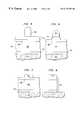
- FIGS. 5 - 8a specific example of the inventive photoresist-less plasma-enhanced metallization etch technique is depicted in FIGS. 5 - 8 .
- metal layer 502which is disposed above a substrate 104 .
- metal layer 502includes three separate layers: a barrier layer 504 , a metal layer 506 , and a barrier/antireflective coating (ARC) layer 508 .
- barrier layer 504 and barrier/ARC layer 508are optional and may not be necessary in every case, depending on the specific choice of materials for metal layer 502 and/or the layers that are adjacent to metal layer 502 .
- barrier layer 504comprises a layer of TiN overlying a Ti layer.
- Metal layer 506represents an aluminum-containing layer, preferably formed of aluminum or one of the aluminum alloys such as Al/Cu or Al/Cu/Si.
- Barrier/ARC layer 508also comprises a layer of TIN overlying a Ti layer.
- a hard mask layer 510formed of a hard mask material such as SiON, oxide, SIN, FOX, or any combination thereof In one particularly advantageous embodiment, the hard mask material is SiON to permit the use of deep UV lithography thereon without requiring an additional organic ARC layer.
- the photoresist maskis then stripped in a conventional photoresist stripping process, such as plasma-enhanced ashing using either O 2 or O 2 /H 2 O vapor as the ashing agent.
- a conventional photoresist stripping processsuch as plasma-enhanced ashing using either O 2 or O 2 /H 2 O vapor as the ashing agent.
- the photoresist maskis employed only to etch through the hard mask layer down to the metal layer.
- the result after photoresist stripis shown in FIG. 7 .
- the pattern of the hard maskis transferred to the metal layer using a suitable etchant.
- a suitable etchantemployed depends of course on the composition of the layers comprising the metal layer. It is desirable that the etchant be selective to the hard mask material while etching through the aluminum layer. By way of example, etchants that include Cl 2 have been found suitable for etching through the aluminum-containing layer.
- the removal of the photoresist mask from the metallization etching processmay adversely affect the etch anisotropy (e.g., the desired vertical etch profile) of the plasma-enhanced etch process (e.g., RIE) since there is no PR-based polymer side wall to protect against mask undercutting.
- the etchant source gas that is employed to etch through the metal layeradvantageously includes, in accordance with one embodiment of the present invention, at least one side wall passivating agent.
- the side wall passivating agentsmay be, for example, N 2 , CH 4 , CHF 3 .
- the aluminum-containing layeris etched in a TCPTM 9600SE plasma processing reactor, which is available from Lam Research Corp. of Fremont, Calif.
- TCPTM 9600SE plasma processing reactorwhich is available from Lam Research Corp. of Fremont, Calif.
- the percentage of N 2 addition to the total-flow of Cl 2 +HClis between about 1% and 50%, preferably between about 5% and 30%, and more preferably between about 10% and 25%.
- the etchmay also be performed in 2 (or more) separate steps (e.g. main etch, and over etch.
Landscapes
- Engineering & Computer Science (AREA)
- Physics & Mathematics (AREA)
- Condensed Matter Physics & Semiconductors (AREA)
- General Physics & Mathematics (AREA)
- Manufacturing & Machinery (AREA)
- Computer Hardware Design (AREA)
- Microelectronics & Electronic Packaging (AREA)
- Power Engineering (AREA)
- Chemical & Material Sciences (AREA)
- General Chemical & Material Sciences (AREA)
- Chemical Kinetics & Catalysis (AREA)
- Plasma & Fusion (AREA)
- Materials Engineering (AREA)
- Mechanical Engineering (AREA)
- Metallurgy (AREA)
- Organic Chemistry (AREA)
- Drying Of Semiconductors (AREA)
- Internal Circuitry In Semiconductor Integrated Circuit Devices (AREA)
Abstract
Description
Claims (15)
Priority Applications (7)
| Application Number | Priority Date | Filing Date | Title |
|---|---|---|---|
| US09/153,390US6177353B1 (en) | 1998-09-15 | 1998-09-15 | Metallization etching techniques for reducing post-etch corrosion of metal lines |
| DE69935100TDE69935100T2 (en) | 1998-09-15 | 1999-08-12 | Process for etching a metallization by means of a hard mask |
| EP99115878AEP0987745B1 (en) | 1998-09-15 | 1999-08-12 | Metallization etching method using a hard mask layer |
| JP25886499AJP4690512B2 (en) | 1998-09-15 | 1999-09-13 | Method for reducing polymer deposition on etched vertical metal lines, corrosion of etched metal lines and corrosion during wet cleaning of etched metal features |
| KR1019990039490AKR100676995B1 (en) | 1998-09-15 | 1999-09-15 | Metallization etching technology to reduce post etch corrosion of metal lines |
| CNB991188624ACN1146967C (en) | 1998-09-15 | 1999-09-15 | Etching technology for reducing corrosion of metal patterns of coated layer on substrate |
| TW088115813ATW457583B (en) | 1998-09-15 | 2000-01-10 | Metallization etching techniques for reducing post-etch corrosion of metal lines |
Applications Claiming Priority (1)
| Application Number | Priority Date | Filing Date | Title |
|---|---|---|---|
| US09/153,390US6177353B1 (en) | 1998-09-15 | 1998-09-15 | Metallization etching techniques for reducing post-etch corrosion of metal lines |
Publications (1)
| Publication Number | Publication Date |
|---|---|
| US6177353B1true US6177353B1 (en) | 2001-01-23 |
Family
ID=22547020
Family Applications (1)
| Application Number | Title | Priority Date | Filing Date |
|---|---|---|---|
| US09/153,390Expired - LifetimeUS6177353B1 (en) | 1998-09-15 | 1998-09-15 | Metallization etching techniques for reducing post-etch corrosion of metal lines |
Country Status (7)
| Country | Link |
|---|---|
| US (1) | US6177353B1 (en) |
| EP (1) | EP0987745B1 (en) |
| JP (1) | JP4690512B2 (en) |
| KR (1) | KR100676995B1 (en) |
| CN (1) | CN1146967C (en) |
| DE (1) | DE69935100T2 (en) |
| TW (1) | TW457583B (en) |
Cited By (32)
| Publication number | Priority date | Publication date | Assignee | Title |
|---|---|---|---|---|
| US6335284B1 (en)* | 1998-09-24 | 2002-01-01 | Samsung Electronics Co., Ltd. | Metallization process for manufacturing semiconductor devices |
| US6348405B1 (en)* | 1999-01-25 | 2002-02-19 | Nec Corporation | Interconnection forming method utilizing an inorganic antireflection layer |
| US6399508B1 (en)* | 1999-01-12 | 2002-06-04 | Applied Materials, Inc. | Method for metal etch using a dielectric hard mask |
| US20020192957A1 (en)* | 2001-05-24 | 2002-12-19 | Lam Research Corporation | Applications of oxide hardmasking in metal dry etch processors |
| US6576562B2 (en)* | 2000-12-15 | 2003-06-10 | Kabushiki Kaisha Toshiba | Manufacturing method of semiconductor device using mask pattern having high etching resistance |
| US20040058541A1 (en)* | 1998-03-12 | 2004-03-25 | Tetsuo Ono | Sample surface processing method |
| US20040157435A1 (en)* | 2003-01-30 | 2004-08-12 | Tae-Hee Park | Methods of forming metal lines in semiconductor devices |
| US20040171272A1 (en)* | 2003-02-28 | 2004-09-02 | Applied Materials, Inc. | Method of etching metallic materials to form a tapered profile |
| US6798065B2 (en)* | 1999-03-24 | 2004-09-28 | Newport Fab, Llc | Method and apparatus for high-resolution in-situ plasma etching of inorganic and metals films |
| US20050014381A1 (en)* | 2003-07-18 | 2005-01-20 | Lee Joon Hyeon | Method of forming metal line layer in semiconductor device |
| US20080094885A1 (en)* | 2006-10-24 | 2008-04-24 | Macronix International Co., Ltd. | Bistable Resistance Random Access Memory Structures with Multiple Memory Layers and Multilevel Memory States |
| US7411170B2 (en) | 2006-08-31 | 2008-08-12 | Canon Kabushiki Kaisha | Photoelectric-conversion apparatus and image-pickup system |
| US8859418B2 (en) | 2012-01-11 | 2014-10-14 | Globalfoundries Inc. | Methods of forming conductive structures using a dual metal hard mask technique |
| US20150079800A1 (en)* | 2013-09-13 | 2015-03-19 | Kabushiki Kaisha Toshiba | Method of manufacturing semiconductor device |
| US20160314985A1 (en)* | 2015-04-24 | 2016-10-27 | Lam Research Corporation | Cobalt etch back |
| US9806252B2 (en) | 2015-04-20 | 2017-10-31 | Lam Research Corporation | Dry plasma etch method to pattern MRAM stack |
| US9837312B1 (en) | 2016-07-22 | 2017-12-05 | Lam Research Corporation | Atomic layer etching for enhanced bottom-up feature fill |
| US9972504B2 (en) | 2015-08-07 | 2018-05-15 | Lam Research Corporation | Atomic layer etching of tungsten for enhanced tungsten deposition fill |
| US9984858B2 (en) | 2015-09-04 | 2018-05-29 | Lam Research Corporation | ALE smoothness: in and outside semiconductor industry |
| US9991128B2 (en) | 2016-02-05 | 2018-06-05 | Lam Research Corporation | Atomic layer etching in continuous plasma |
| US9997371B1 (en) | 2017-04-24 | 2018-06-12 | Lam Research Corporation | Atomic layer etch methods and hardware for patterning applications |
| US10096487B2 (en) | 2015-08-19 | 2018-10-09 | Lam Research Corporation | Atomic layer etching of tungsten and other metals |
| US10186426B2 (en) | 2015-01-12 | 2019-01-22 | Lam Research Corporation | Integrating atomic scale processes: ALD (atomic layer deposition) and ale (atomic layer etch) |
| US10269566B2 (en) | 2016-04-29 | 2019-04-23 | Lam Research Corporation | Etching substrates using ale and selective deposition |
| US10559475B2 (en) | 2016-02-04 | 2020-02-11 | Lam Research Corporation | Control of directionality in atomic layer etching |
| US10559461B2 (en) | 2017-04-19 | 2020-02-11 | Lam Research Corporation | Selective deposition with atomic layer etch reset |
| US10566212B2 (en) | 2016-12-19 | 2020-02-18 | Lam Research Corporation | Designer atomic layer etching |
| US10727073B2 (en) | 2016-02-04 | 2020-07-28 | Lam Research Corporation | Atomic layer etching 3D structures: Si and SiGe and Ge smoothness on horizontal and vertical surfaces |
| US10832909B2 (en) | 2017-04-24 | 2020-11-10 | Lam Research Corporation | Atomic layer etch, reactive precursors and energetic sources for patterning applications |
| US11450513B2 (en) | 2018-03-30 | 2022-09-20 | Lam Research Corporation | Atomic layer etching and smoothing of refractory metals and other high surface binding energy materials |
| US20240429064A1 (en)* | 2023-06-26 | 2024-12-26 | Taiwan Semiconductor Manufacturing Company, Ltd. | Metal etching with reduced tilt angle |
| US12444651B2 (en) | 2022-06-28 | 2025-10-14 | Novellus Systems, Inc. | Tungsten feature fill with nucleation inhibition |
Families Citing this family (17)
| Publication number | Priority date | Publication date | Assignee | Title |
|---|---|---|---|---|
| DE10062639A1 (en)* | 2000-12-15 | 2002-07-04 | Infineon Technologies Ag | Production of conducting pathways, especially aluminum pathways used in CMOS circuits or DRAM cells comprises applying an aluminum conducting layer, a titanium nitride layer and a lacquer mask onto a substrate, and structuring |
| KR100402239B1 (en)* | 2001-06-30 | 2003-10-17 | 주식회사 하이닉스반도체 | Method of fabricating metal gate of semiconductor device |
| SG96644A1 (en)* | 2001-09-11 | 2003-06-16 | Chartered Semiconductor Mfg | Etch/clean process for integrated circuit pad metal |
| KR100464430B1 (en)* | 2002-08-20 | 2005-01-03 | 삼성전자주식회사 | Method of etching aluminum layer using hard mask and metalization method for semiconductor device |
| DE60310528T2 (en)* | 2003-05-07 | 2007-09-27 | Stmicroelectronics S.R.L., Agrate Brianza | A method for defining a chalcogenide material layer, in particular in a method for producing phase change memory cells |
| US20060169968A1 (en)* | 2005-02-01 | 2006-08-03 | Thomas Happ | Pillar phase change memory cell |
| US20100003828A1 (en)* | 2007-11-28 | 2010-01-07 | Guowen Ding | Methods for adjusting critical dimension uniformity in an etch process with a highly concentrated unsaturated hydrocarbon gas |
| US8748323B2 (en) | 2008-07-07 | 2014-06-10 | Macronix International Co., Ltd. | Patterning method |
| US9683305B2 (en)* | 2011-12-20 | 2017-06-20 | Apple Inc. | Metal surface and process for treating a metal surface |
| CN102723273B (en)* | 2012-05-28 | 2015-03-11 | 上海华力微电子有限公司 | Method for enlarging corrosion defect process window of dry etching of aluminum wire |
| CN102820261A (en)* | 2012-08-22 | 2012-12-12 | 上海宏力半导体制造有限公司 | Aluminum etching method |
| US9633867B2 (en)* | 2015-01-05 | 2017-04-25 | Lam Research Corporation | Method and apparatus for anisotropic tungsten etching |
| CN104658905B (en)* | 2015-02-27 | 2018-01-05 | 深圳市华星光电技术有限公司 | A kind of lithographic method and substrate |
| JP6785101B2 (en)* | 2016-09-09 | 2020-11-18 | 東京エレクトロン株式会社 | Plasma etching method |
| TWI812762B (en)* | 2018-07-30 | 2023-08-21 | 日商東京威力科創股份有限公司 | Method, device and system for processing object |
| CN114156178A (en)* | 2020-09-04 | 2022-03-08 | 中芯集成电路(宁波)有限公司 | Method for forming semiconductor structure |
| CN115938937B (en)* | 2023-03-09 | 2023-06-09 | 合肥晶合集成电路股份有限公司 | Semiconductor structure and preparation method thereof |
Citations (14)
| Publication number | Priority date | Publication date | Assignee | Title |
|---|---|---|---|---|
| US5211804A (en) | 1990-10-16 | 1993-05-18 | Oki Electric Industry, Co., Ltd. | Method for dry etching |
| US5270254A (en)* | 1991-03-27 | 1993-12-14 | Sgs-Thomson Microelectronics, Inc. | Integrated circuit metallization with zero contact enclosure requirements and method of making the same |
| US5277750A (en)* | 1991-03-05 | 1994-01-11 | Siemens Aktiengesellschaft | Method for anisotropic dry etching of metallization layers, containing aluminum or aluminum alloys, in integrated semiconductor circuits |
| GB2286721A (en) | 1994-02-15 | 1995-08-23 | Nec Corp | Method for fabricating semiconductor device |
| US5545289A (en) | 1994-02-03 | 1996-08-13 | Applied Materials, Inc. | Passivating, stripping and corrosion inhibition of semiconductor substrates |
| US5573973A (en)* | 1993-03-19 | 1996-11-12 | National Semiconductor Corporation | Integrated circuit having a diamond thin film trench arrangement as a component thereof and method |
| US5654233A (en)* | 1996-04-08 | 1997-08-05 | Taiwan Semiconductor Manufacturing Company Ltd | Step coverage enhancement process for sub half micron contact/via |
| US5741741A (en)* | 1996-05-23 | 1998-04-21 | Vanguard International Semiconductor Corporation | Method for making planar metal interconnections and metal plugs on semiconductor substrates |
| US5779926A (en)* | 1994-09-16 | 1998-07-14 | Applied Materials, Inc. | Plasma process for etching multicomponent alloys |
| US5792687A (en)* | 1996-08-01 | 1998-08-11 | Vanguard International Semiconductor Corporation | Method for fabricating high density integrated circuits using oxide and polysilicon spacers |
| US5801082A (en)* | 1997-08-18 | 1998-09-01 | Vanguard International Semiconductor Corporation | Method for making improved shallow trench isolation with dielectric studs for semiconductor integrated circuits |
| US5827437A (en)* | 1996-05-17 | 1998-10-27 | Lam Research Corporation | Multi-step metallization etch |
| US5834805A (en)* | 1995-12-06 | 1998-11-10 | Micron Technology, Inc. | Dynamic random access memory circuit array and memory cell |
| US5920799A (en)* | 1994-12-29 | 1999-07-06 | Graves'trust Group | Method for the treatment of substrates |
Family Cites Families (11)
| Publication number | Priority date | Publication date | Assignee | Title |
|---|---|---|---|---|
| JPS6033367A (en)* | 1983-08-04 | 1985-02-20 | Nec Corp | Dry etching method of aluminum |
| JPH05166756A (en)* | 1991-12-12 | 1993-07-02 | Hitachi Ltd | Etching apparatus |
| US5387556A (en)* | 1993-02-24 | 1995-02-07 | Applied Materials, Inc. | Etching aluminum and its alloys using HC1, C1-containing etchant and N.sub.2 |
| JP3161888B2 (en)* | 1993-09-17 | 2001-04-25 | 株式会社日立製作所 | Dry etching method |
| JPH07249607A (en)* | 1994-03-14 | 1995-09-26 | Fujitsu Ltd | Method for manufacturing semiconductor device |
| JP3353524B2 (en)* | 1995-03-22 | 2002-12-03 | ソニー株式会社 | Method for manufacturing semiconductor device including step of forming connection hole |
| JP3112832B2 (en)* | 1996-05-30 | 2000-11-27 | 日本電気株式会社 | Method for manufacturing semiconductor device |
| US5976986A (en)* | 1996-08-06 | 1999-11-02 | International Business Machines Corp. | Low pressure and low power C12 /HC1 process for sub-micron metal etching |
| JP3258240B2 (en)* | 1996-09-10 | 2002-02-18 | 株式会社日立製作所 | Etching method |
| JP3006508B2 (en)* | 1996-10-15 | 2000-02-07 | 日本電気株式会社 | Method for etching aluminum film or aluminum alloy film |
| KR100255663B1 (en)* | 1997-12-11 | 2000-05-01 | 윤종용 | Method for etching al film and forming metallization layer of semiconductor device |
- 1998
- 1998-09-15USUS09/153,390patent/US6177353B1/ennot_activeExpired - Lifetime
- 1999
- 1999-08-12DEDE69935100Tpatent/DE69935100T2/ennot_activeExpired - Lifetime
- 1999-08-12EPEP99115878Apatent/EP0987745B1/ennot_activeExpired - Lifetime
- 1999-09-13JPJP25886499Apatent/JP4690512B2/ennot_activeExpired - Fee Related
- 1999-09-15KRKR1019990039490Apatent/KR100676995B1/ennot_activeExpired - Fee Related
- 1999-09-15CNCNB991188624Apatent/CN1146967C/ennot_activeExpired - Fee Related
- 2000
- 2000-01-10TWTW088115813Apatent/TW457583B/ennot_activeIP Right Cessation
Patent Citations (15)
| Publication number | Priority date | Publication date | Assignee | Title |
|---|---|---|---|---|
| US5211804A (en) | 1990-10-16 | 1993-05-18 | Oki Electric Industry, Co., Ltd. | Method for dry etching |
| US5277750A (en)* | 1991-03-05 | 1994-01-11 | Siemens Aktiengesellschaft | Method for anisotropic dry etching of metallization layers, containing aluminum or aluminum alloys, in integrated semiconductor circuits |
| US5270254A (en)* | 1991-03-27 | 1993-12-14 | Sgs-Thomson Microelectronics, Inc. | Integrated circuit metallization with zero contact enclosure requirements and method of making the same |
| US5371410A (en)* | 1991-03-27 | 1994-12-06 | Sgs-Thomson Microelectronics, Inc. | Integrated circuit metallization with zero contact enclosure requirements |
| US5573973A (en)* | 1993-03-19 | 1996-11-12 | National Semiconductor Corporation | Integrated circuit having a diamond thin film trench arrangement as a component thereof and method |
| US5545289A (en) | 1994-02-03 | 1996-08-13 | Applied Materials, Inc. | Passivating, stripping and corrosion inhibition of semiconductor substrates |
| GB2286721A (en) | 1994-02-15 | 1995-08-23 | Nec Corp | Method for fabricating semiconductor device |
| US5779926A (en)* | 1994-09-16 | 1998-07-14 | Applied Materials, Inc. | Plasma process for etching multicomponent alloys |
| US5920799A (en)* | 1994-12-29 | 1999-07-06 | Graves'trust Group | Method for the treatment of substrates |
| US5834805A (en)* | 1995-12-06 | 1998-11-10 | Micron Technology, Inc. | Dynamic random access memory circuit array and memory cell |
| US5654233A (en)* | 1996-04-08 | 1997-08-05 | Taiwan Semiconductor Manufacturing Company Ltd | Step coverage enhancement process for sub half micron contact/via |
| US5827437A (en)* | 1996-05-17 | 1998-10-27 | Lam Research Corporation | Multi-step metallization etch |
| US5741741A (en)* | 1996-05-23 | 1998-04-21 | Vanguard International Semiconductor Corporation | Method for making planar metal interconnections and metal plugs on semiconductor substrates |
| US5792687A (en)* | 1996-08-01 | 1998-08-11 | Vanguard International Semiconductor Corporation | Method for fabricating high density integrated circuits using oxide and polysilicon spacers |
| US5801082A (en)* | 1997-08-18 | 1998-09-01 | Vanguard International Semiconductor Corporation | Method for making improved shallow trench isolation with dielectric studs for semiconductor integrated circuits |
Cited By (50)
| Publication number | Priority date | Publication date | Assignee | Title |
|---|---|---|---|---|
| US7259104B2 (en)* | 1998-03-12 | 2007-08-21 | Hitachi, Ltd. | Sample surface processing method |
| US20040058541A1 (en)* | 1998-03-12 | 2004-03-25 | Tetsuo Ono | Sample surface processing method |
| US6335284B1 (en)* | 1998-09-24 | 2002-01-01 | Samsung Electronics Co., Ltd. | Metallization process for manufacturing semiconductor devices |
| US6399508B1 (en)* | 1999-01-12 | 2002-06-04 | Applied Materials, Inc. | Method for metal etch using a dielectric hard mask |
| US6348405B1 (en)* | 1999-01-25 | 2002-02-19 | Nec Corporation | Interconnection forming method utilizing an inorganic antireflection layer |
| US6798065B2 (en)* | 1999-03-24 | 2004-09-28 | Newport Fab, Llc | Method and apparatus for high-resolution in-situ plasma etching of inorganic and metals films |
| US6576562B2 (en)* | 2000-12-15 | 2003-06-10 | Kabushiki Kaisha Toshiba | Manufacturing method of semiconductor device using mask pattern having high etching resistance |
| US6921493B2 (en)* | 2001-05-24 | 2005-07-26 | Lam Research Corporation | Method of processing substrates |
| US20020192957A1 (en)* | 2001-05-24 | 2002-12-19 | Lam Research Corporation | Applications of oxide hardmasking in metal dry etch processors |
| US20040157435A1 (en)* | 2003-01-30 | 2004-08-12 | Tae-Hee Park | Methods of forming metal lines in semiconductor devices |
| US7001843B2 (en)* | 2003-01-30 | 2006-02-21 | Dongbuanam Semiconductor, Inc. | Methods of forming metal lines in semiconductor devices |
| US20040171272A1 (en)* | 2003-02-28 | 2004-09-02 | Applied Materials, Inc. | Method of etching metallic materials to form a tapered profile |
| US20050014381A1 (en)* | 2003-07-18 | 2005-01-20 | Lee Joon Hyeon | Method of forming metal line layer in semiconductor device |
| US7148150B2 (en)* | 2003-07-18 | 2006-12-12 | Hynix Semiconductor Inc. | Method of forming metal line layer in semiconductor device |
| US7592578B2 (en) | 2006-08-31 | 2009-09-22 | Canon Kabushiki Kaisha | Photoelectric-conversion apparatus and image-pickup system |
| US7411170B2 (en) | 2006-08-31 | 2008-08-12 | Canon Kabushiki Kaisha | Photoelectric-conversion apparatus and image-pickup system |
| US20090011532A1 (en)* | 2006-08-31 | 2009-01-08 | Canon Kabushiki Kaisha | Photoelectric-conversion apparatus and image-pickup system |
| US20080094885A1 (en)* | 2006-10-24 | 2008-04-24 | Macronix International Co., Ltd. | Bistable Resistance Random Access Memory Structures with Multiple Memory Layers and Multilevel Memory States |
| US8859418B2 (en) | 2012-01-11 | 2014-10-14 | Globalfoundries Inc. | Methods of forming conductive structures using a dual metal hard mask technique |
| US20150079800A1 (en)* | 2013-09-13 | 2015-03-19 | Kabushiki Kaisha Toshiba | Method of manufacturing semiconductor device |
| US10186426B2 (en) | 2015-01-12 | 2019-01-22 | Lam Research Corporation | Integrating atomic scale processes: ALD (atomic layer deposition) and ale (atomic layer etch) |
| US10515816B2 (en) | 2015-01-12 | 2019-12-24 | Lam Research Corporation | Integrating atomic scale processes: ALD (atomic layer deposition) and ALE (atomic layer etch) |
| US9806252B2 (en) | 2015-04-20 | 2017-10-31 | Lam Research Corporation | Dry plasma etch method to pattern MRAM stack |
| US10749103B2 (en) | 2015-04-20 | 2020-08-18 | Lam Research Corporation | Dry plasma etch method to pattern MRAM stack |
| US10374144B2 (en) | 2015-04-20 | 2019-08-06 | Lam Research Corporation | Dry plasma etch method to pattern MRAM stack |
| US20160314985A1 (en)* | 2015-04-24 | 2016-10-27 | Lam Research Corporation | Cobalt etch back |
| US10784086B2 (en) | 2015-04-24 | 2020-09-22 | Lam Research Corporation | Cobalt etch back |
| US9870899B2 (en)* | 2015-04-24 | 2018-01-16 | Lam Research Corporation | Cobalt etch back |
| US9972504B2 (en) | 2015-08-07 | 2018-05-15 | Lam Research Corporation | Atomic layer etching of tungsten for enhanced tungsten deposition fill |
| US11069535B2 (en) | 2015-08-07 | 2021-07-20 | Lam Research Corporation | Atomic layer etch of tungsten for enhanced tungsten deposition fill |
| US10096487B2 (en) | 2015-08-19 | 2018-10-09 | Lam Research Corporation | Atomic layer etching of tungsten and other metals |
| US10304659B2 (en) | 2015-09-04 | 2019-05-28 | Lam Research Corporation | Ale smoothness: in and outside semiconductor industry |
| US9984858B2 (en) | 2015-09-04 | 2018-05-29 | Lam Research Corporation | ALE smoothness: in and outside semiconductor industry |
| US10559475B2 (en) | 2016-02-04 | 2020-02-11 | Lam Research Corporation | Control of directionality in atomic layer etching |
| US10727073B2 (en) | 2016-02-04 | 2020-07-28 | Lam Research Corporation | Atomic layer etching 3D structures: Si and SiGe and Ge smoothness on horizontal and vertical surfaces |
| US9991128B2 (en) | 2016-02-05 | 2018-06-05 | Lam Research Corporation | Atomic layer etching in continuous plasma |
| US10685836B2 (en) | 2016-04-29 | 2020-06-16 | Lam Research Corporation | Etching substrates using ALE and selective deposition |
| US10269566B2 (en) | 2016-04-29 | 2019-04-23 | Lam Research Corporation | Etching substrates using ale and selective deposition |
| US9837312B1 (en) | 2016-07-22 | 2017-12-05 | Lam Research Corporation | Atomic layer etching for enhanced bottom-up feature fill |
| US11239094B2 (en) | 2016-12-19 | 2022-02-01 | Lam Research Corporation | Designer atomic layer etching |
| US10566212B2 (en) | 2016-12-19 | 2020-02-18 | Lam Research Corporation | Designer atomic layer etching |
| US10566213B2 (en) | 2016-12-19 | 2020-02-18 | Lam Research Corporation | Atomic layer etching of tantalum |
| US11721558B2 (en) | 2016-12-19 | 2023-08-08 | Lam Research Corporation | Designer atomic layer etching |
| US10559461B2 (en) | 2017-04-19 | 2020-02-11 | Lam Research Corporation | Selective deposition with atomic layer etch reset |
| US10998187B2 (en) | 2017-04-19 | 2021-05-04 | Lam Research Corporation | Selective deposition with atomic layer etch reset |
| US10832909B2 (en) | 2017-04-24 | 2020-11-10 | Lam Research Corporation | Atomic layer etch, reactive precursors and energetic sources for patterning applications |
| US9997371B1 (en) | 2017-04-24 | 2018-06-12 | Lam Research Corporation | Atomic layer etch methods and hardware for patterning applications |
| US11450513B2 (en) | 2018-03-30 | 2022-09-20 | Lam Research Corporation | Atomic layer etching and smoothing of refractory metals and other high surface binding energy materials |
| US12444651B2 (en) | 2022-06-28 | 2025-10-14 | Novellus Systems, Inc. | Tungsten feature fill with nucleation inhibition |
| US20240429064A1 (en)* | 2023-06-26 | 2024-12-26 | Taiwan Semiconductor Manufacturing Company, Ltd. | Metal etching with reduced tilt angle |
Also Published As
| Publication number | Publication date |
|---|---|
| CN1270415A (en) | 2000-10-18 |
| KR100676995B1 (en) | 2007-01-31 |
| KR20000023166A (en) | 2000-04-25 |
| DE69935100T2 (en) | 2007-12-13 |
| JP2000323483A (en) | 2000-11-24 |
| EP0987745B1 (en) | 2007-02-14 |
| DE69935100D1 (en) | 2007-03-29 |
| CN1146967C (en) | 2004-04-21 |
| TW457583B (en) | 2001-10-01 |
| JP4690512B2 (en) | 2011-06-01 |
| EP0987745A1 (en) | 2000-03-22 |
Similar Documents
| Publication | Publication Date | Title |
|---|---|---|
| US6177353B1 (en) | Metallization etching techniques for reducing post-etch corrosion of metal lines | |
| US7468319B2 (en) | Method for preventing a metal corrosion in a semiconductor device | |
| US20060128159A1 (en) | Method of removing etch residues | |
| US20040180551A1 (en) | Carbon hard mask for aluminum interconnect fabrication | |
| US5792672A (en) | Photoresist strip method | |
| KR100450564B1 (en) | Post treatment method for metal line of semiconductor device | |
| JP3318801B2 (en) | Dry etching method | |
| US6420099B1 (en) | Tungsten hard mask for dry etching aluminum-containing layers | |
| US6043163A (en) | HCL in overetch with hard mask to improve metal line etching profile | |
| US20050181604A1 (en) | Method for structuring metal by means of a carbon mask | |
| US5741742A (en) | Formation of aluminum-alloy pattern | |
| US20040038547A1 (en) | Method of etching a metal layer using a mask, a metallization method for a semiconductor device, a method of etching a metal layer, and an etching gas | |
| US6103630A (en) | Adding SF6 gas to improve metal undercut for hardmask metal etching | |
| US6077777A (en) | Method for forming wires of semiconductor device | |
| JP3082396B2 (en) | Method for manufacturing semiconductor device | |
| HK1023648A (en) | Metallization etching method using a hard mask layer | |
| KR19980044194A (en) | Metal wiring formation method of semiconductor device | |
| US20030228755A1 (en) | Method for metal patterning and improved linewidth control | |
| JPH05182937A (en) | Dry-etching method | |
| KR0141172B1 (en) | Metal wiring formation method | |
| KR100259072B1 (en) | Method for forming metal gate | |
| JP2708019B2 (en) | Contact hole formation method | |
| KR100467817B1 (en) | Method for preventing metal corrosion of semiconductor | |
| JP3541329B2 (en) | Dry etching method | |
| KR20020068621A (en) | Method for manufacturing interconnection of semiconductor device |
Legal Events
| Date | Code | Title | Description |
|---|---|---|---|
| AS | Assignment | Owner name:SIEMENS MICROELECTRONICS, INC., CALIFORNIA Free format text:ASSIGNMENT OF ASSIGNORS INTEREST;ASSIGNOR:STOJAKOVIC, GEORG;REEL/FRAME:009854/0610 Effective date:19990212 Owner name:SIEMENS MICROELECTRONICS, INC., CALIFORNIA Free format text:ASSIGNMENT OF ASSIGNORS INTEREST;ASSIGNOR:SPULER, BRUNO;REEL/FRAME:009854/0614 Effective date:19990308 Owner name:SIEMENS MICROELECTRONICS, INC., CALIFORNIA Free format text:ASSIGNMENT OF ASSIGNORS INTEREST;ASSIGNOR:LUEKEN, EIKE;REEL/FRAME:009854/0752 Effective date:19990212 Owner name:SIEMENS MICROELECTRONICS, INC., CALIFORNIA Free format text:ASSIGNMENT OF ASSIGNORS INTEREST;ASSIGNOR:GUTSCHE, MARTIN;REEL/FRAME:009855/0135 Effective date:19990215 Owner name:SIEMENS MICROELECTRONICS, INC., CALIFORNIA Free format text:ASSIGNMENT OF ASSIGNORS INTEREST;ASSIGNOR:WEGE, STEPHAN;REEL/FRAME:009853/0736 Effective date:19990222 Owner name:SIEMENS MICROELECTRONICS, INC., CALIFORNIA Free format text:ASSIGNMENT OF ASSIGNORS INTEREST;ASSIGNOR:STROBL, PETER;REEL/FRAME:009856/0704 Effective date:19990212 | |
| AS | Assignment | Owner name:INFINEON TECHNOLOGIES CORPORATION, CALIFORNIA Free format text:CHANGE OF NAME;ASSIGNOR:SIEMENS DRAM SEMICONDUCTOR CORPORATION;REEL/FRAME:010244/0915 Effective date:19990401 Owner name:SIEMENS AKTIENGESELLSCHAFT, GERMANY Free format text:ASSIGNMENT OF ASSIGNORS INTEREST;ASSIGNOR:INFINEON TECHNOLOGIES CORPORATION;REEL/FRAME:010244/0923 Effective date:19990623 Owner name:SMI HOLDING LLC, CALIFORNIA Free format text:MERGER;ASSIGNOR:SIEMENS MICROELECTRONICS, INC.;REEL/FRAME:010244/0900 Effective date:19990330 Owner name:SIEMENS DRAM SEMICONDUCTOR CORPORATION, CALIFORNIA Free format text:TRANSFER OF ASSETS;ASSIGNOR:SMI HOLDING LLC;REEL/FRAME:010244/0877 Effective date:19990330 | |
| AS | Assignment | Owner name:INFINEON TECHNOLOGIES CORPORATION, CALIFORNIA Free format text:ASSIGNMENT OF ASSIGNORS INTEREST;ASSIGNORS:GUTSCHE, MARTIN;STROBL, PETER;WEGE, STEPHAN;AND OTHERS;REEL/FRAME:010491/0299;SIGNING DATES FROM 19990410 TO 19991101 | |
| STCF | Information on status: patent grant | Free format text:PATENTED CASE | |
| FPAY | Fee payment | Year of fee payment:4 | |
| FPAY | Fee payment | Year of fee payment:8 | |
| AS | Assignment | Owner name:QIMONDA AG,GERMANY Free format text:ASSIGNMENT OF ASSIGNORS INTEREST;ASSIGNOR:INFINEON TECHNOLOGIES AG;REEL/FRAME:024456/0001 Effective date:20060425 | |
| FPAY | Fee payment | Year of fee payment:12 | |
| AS | Assignment | Owner name:INFINEON TECHNOLOGIES AG, GERMANY Free format text:ASSIGNMENT OF ASSIGNORS INTEREST;ASSIGNOR:QIMONDA AG;REEL/FRAME:035623/0001 Effective date:20141009 | |
| AS | Assignment | Owner name:POLARIS INNOVATIONS LIMITED, IRELAND Free format text:ASSIGNMENT OF ASSIGNORS INTEREST;ASSIGNOR:INFINEON TECHNOLOGIES AG;REEL/FRAME:036353/0134 Effective date:20150708 |