US6175893B1 - High bandwidth code/data access using slow memory - Google Patents
High bandwidth code/data access using slow memoryDownload PDFInfo
- Publication number
- US6175893B1 US6175893B1US09/066,077US6607798AUS6175893B1US 6175893 B1US6175893 B1US 6175893B1US 6607798 AUS6607798 AUS 6607798AUS 6175893 B1US6175893 B1US 6175893B1
- Authority
- US
- United States
- Prior art keywords
- address
- memory
- microcontroller
- read
- program code
- Prior art date
- Legal status (The legal status is an assumption and is not a legal conclusion. Google has not performed a legal analysis and makes no representation as to the accuracy of the status listed.)
- Expired - Fee Related
Links
Images


Classifications
- G—PHYSICS
- G06—COMPUTING OR CALCULATING; COUNTING
- G06F—ELECTRIC DIGITAL DATA PROCESSING
- G06F12/00—Accessing, addressing or allocating within memory systems or architectures
- G06F12/02—Addressing or allocation; Relocation
- G06F12/0215—Addressing or allocation; Relocation with look ahead addressing means
- G—PHYSICS
- G06—COMPUTING OR CALCULATING; COUNTING
- G06F—ELECTRIC DIGITAL DATA PROCESSING
- G06F12/00—Accessing, addressing or allocating within memory systems or architectures
- G06F12/02—Addressing or allocation; Relocation
- G06F12/06—Addressing a physical block of locations, e.g. base addressing, module addressing, memory dedication
- G06F12/0607—Interleaved addressing
Definitions
- the inventionpertains to the field of disk drive controllers. More particularly, the present invention pertains to disk drive microcontrollers, read only program code memory and the interface therebetween.
- the microcontroller and code memoryare evenly matched. Under such a state, the microcontroller requests a program code word from the code memory by supplying the code memory with the address of the program code word requested. The code memory then decodes the address and supplies the microcontroller with the program code word located at the address supplied by the microcontroller as soon as the microcontroller is able to process it.
- an object of the present inventionto provide circuits for efficiently supplying code words from a slow code memory to a relatively faster microcontroller.
- a read-only memoryis connectable to a microcontroller data bus and address bus, and comprises memory circuits for storing a sequential array of code words executable by the microcontroller; memory address decoding circuits for selecting one code word of the array of code words; circuits for conveying the selected one code word to the data bus when a read signal is received from the microcontroller; circuits for storing an address transmitted on the address bus by the microcontroller when an address latch signal is asserted by the microcontroller, the stored address being connected to the memory address decoding circuits; and circuits for incrementing the stored address each time a read signal is received from the microcontroller.
- the read-only memorymay further comprise a ready circuit having a ready state and a not-ready state for delaying the microcontroller when the not-ready state is asserted.
- the not-ready statemay be asserted by the ready circuit when a read signal is received immediately after an address is stored.
- the ready statemay be asserted by the ready circuit immediately when a read signal is received subsequent to a read operation from the stored address.
- the memory circuitsmay comprise an odd array and an even array.
- the address storing circuitsmay comprise odd address storage circuits connected to the odd array and even address storage circuits connected to the even array.
- the stored address incrementing circuitsmay increment the even address storage circuits when the address transmitted by the microcontroller is odd.
- Another embodiment of the present inventionis a microcontroller for executing a program stored sequentially in a read-only memory, the microcontroller comprising an address bus for providing a next program code word address to the read-only memory; circuits for providing an address latch enable signal to the read-only memory for latching the program code word address; circuits for providing a read signal to the read-only memory; and circuits for suppressing the address latch enable signal when the next program code word address is consecutive with an immediately preceding program code word address.
- a further embodiment of the present inventionis a disk drive having a controller, the controller comprising a read only memory and a microcontroller for executing a program stored sequentially in the read-only memory, wherein the microcontroller includes an address bus for providing a next program code word address to the read-only memory, circuits for providing an address latch enable signal to the read-only memory for latching the program code word address, circuits for providing a read signal to the read-only memory, and circuits for suppressing the address latch enable signal when the next program code word address is consecutive with an immediately preceding program code word address; and wherein the read only memory is connected to a microcontroller data bus and to the address bus, the read only memory including memory circuits for storing a sequential array of code words executable by the microcontroller, memory address decoding circuits for selecting one code word of the array of code words, circuits for conveying the selected one code word to the data bus when a read signal is received from the microcontroller, circuits for storing an address transmitted on the address bus by the microcontroller
- the memory circuitsmay include an even memory array and an odd memory array.
- the conveying circuitsmay include a multiplexer for selecting the one code word from outputs of the even and odd memory arrays.
- the storing circuitsmay include at least one register.
- the storing circuitsmay include at least one counter and the incrementing circuits may be integral with the at least one counter.
- the address bus and the data busmay be multiplexed.
- FIG. 1is a block diagram of a microcontroller and of a program code memory according to one embodiment of the present invention.
- FIG. 2shows a disk drive according to another embodiment of the present invention.
- FIG. 3is a block diagram of an embodiment of the program code memory according to the present invention.
- FIG. 4is a timing diagram illustrating the operation of the microcontroller and of the program code memory according to the present invention.
- FIG. 5shows a circuit to generate signals to clock the even and odd address storing registers shown in FIG. 3 .
- FIG. 6shows circuits to generate the Miss and Odd signals used respectively in the program code memory to initiate loading a new address into the address storage registers and to select between odd and even memory arrays.
- Linear codeat least within the context of the present invention, generally refers to code in which consecutively executed instructions are stored at contiguous memory locations. This means that linear code consists of program code words whose addresses are consecutive. Most program code is at least piece-wise linear. Indeed, apart from relatively infrequent instances of non-linear code, the address of the next program code word can be obtained by adding 1 to the address of the preceding program code word. Examples of non-linear code include those instances where a break in the linearity of the code is initiated by a GOTO instruction, a jump instruction, a procedure or function call and the like. In these situations, execution of the program stored within the code memory jumps to another portion of the code.
- a typical memory access cycleconsists of the microcontroller placing an address on an is address bus, the microcontroller asserting an Address Latch Enable (hereafter ALE) signal, the memory decoding and accessing the word stored at the specified address, and the memory placing the word on a data bus for the microcontroller to retrieve.
- ALEAddress Latch Enable
- the present inventionexploits the piece-wise linearity of program code described above to achieve significant speed advantages. For linear portions of the program code, the present invention dispenses with the first and second steps; namely, the placement of an address on the address bus by the microcontroller and the assertion of the ALE signal.
- the program code memoryincludes address storing means for storing a program code word address provided on the address bus by the microcontroller when an address latch signal is asserted by the microcontroller.
- the stored addressis connected to the memory address decoding circuits.
- the program code memorymay self-generate program code word addresses of the next required program code words. Thereafter, program code words corresponding to the self-generated addresses are accessed and placed on a data bus for the microcontroller to retrieve.
- the program code memoryindependently generates the address of the next required program code word, then accesses and places the corresponding program code word on the data bus. In this manner, the microcontroller need not place the address of the next required program code word on the address bus when the address is consecutive with an immediately preceding program code word address, nor need the microcontroller assert the ALE signal. This achieves significant speed advantages because, as long as the address latch signal is not asserted by the microcontroller, the program code memory places a stream of program code words onto the data bus responsive to read commands originating from the microcontroller, without further time consuming input of addresses from the microcontroller or ALE signal assertions.
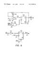
- FIG. 1shows a conceptual block diagram of a microcontroller 110 according to the present invention, a program code memory 120 according to the present invention, as well as interconnections therebetween.
- the transfer of address and data information between microcontroller 110 and program code memory 120may be implemented on separate busses such as address bus 170 and data bus 173 , shown in dotted line form, or may preferably be implemented as a time multiplexed address/data bus 174 .
- the microcontroller 110includes an ALE signal suppressing circuit 150 .
- the ALE suppressing circuit 150suppresses the ALE signal 175 and preferably internal associated logic states when the next program code word address is consecutive with an immediately preceding program code word address.
- the microcontroller 110asserts the ALE signal 175 only when the next required program code word address is not consecutive with the immediately preceding program code word address.
- An asserted ALE signal 175therefore, alerts the program code memory 120 that the next required program code word is non-consecutive. This is done by asserting the Chip Select signal 172 (hereafter CS- signal) and by latching the address transmitted on the address bus 170 or the address/data bus 174 by the microcontroller within the address storing circuit 160 in the program code memory 120 .
- the microcontroller 110when the next required program code word is non-consecutive relative to an immediately preceding program code word, the microcontroller 110 asserts the ALE signal 175 and CS- signal 172 and places the next required program code word address onto the address bus 170 or the address/data bus 174 .
- the program code memory 120then stores the address in the address storing circuit 160 . If the read signal 171 (hereafter RD- signal) is asserted, a ready circuit 140 assumes a not-ready state immediately after the program code word address is stored in the address storing circuit 160 .
- the address storing circuit 160may be, for example, a register or a counter.
- This not-ready statecauses the ready circuit 140 to de-assert the READY signal 176 , thereby delaying the microcontroller 110 while the stored address is stored, and a code word is accessed in the program code memory 120 , and placed on the data bus 173 or on the address/data bus 174 .
- the ready circuit 140may assert the READY signal 176 immediately when the RD- signal 171 is received after an initial read operation from the stored address.
- ready circuit 140may be implemented in microcontroller 110 , providing for pre-determined wait states during memory cycles which access program code memory 120 .
- Ready signal 176is not required to be connected between microcontroller 110 and program code memory 120 .
- the ALE suppressing circuit 150 of the microcontroller 110suppresses the ALE signal 175 and may preferably bypass internal logic states, such as those generating now unnecessary address bus cycles, prior to asserting the read signal RD- 171 .
- the ALE suppressing circuit 150may comprise comparator circuits which can determine that an address for a current read operation is consecutive with an immediately preceding address for a read operation. Numerous implementations of the ALE suppressing circuit 150 are possible and would be apparent to one skilled in the art.
- ALE suppressing circuit 150is integral to microcontroller 110 , however the invention can still be used to advantage with an embodiment of the ALE suppressing circuit 150 , external to microcontroller 110 , which can suppress ALE signal 175 .
- the address storing circuit 160 of the program code memory 120increments the address stored therein by 1, thereby generating the next required address for the next required program code word. This incremented address is then decoded by memory array 130 , and the corresponding code word is accessed and placed on the data bus 173 or the address/data bus 174 for retrieval by the microcontroller 110 .
- the microcontroller 110is informed that the next required code word is available on the data bus 173 or the address/data bus 174 , as the ready circuit 140 of the program code memory 120 asserts the READY signal 176 as soon as it receives the RD- signal 171 subsequent to the previous read operation from the address stored in the address storing circuit 160 .
- the separate address bus 170 and the data bus 173 shown in dashed lines in FIG. 1may be replaced by the multiplexed address/data bus 174 .
- This embodimenthas the advantage, among others, of reducing the number of pins of the pair of devices, by not requiring the separate address and data buses 170 and 173 , respectively.
- the present inventionhas the advantage of eliminating overhead cycles for switching the bus between address and data modes and therefore dynamically extending the period of time in which the multiplexed address/data bus 174 functions as a data bus. Indeed, it is only when the next required program code word address is non-consecutive with an immediately preceding program code word address that the address/data bus 174 functions as an address bus. At other times, the address/data bus 174 transmits a succession of program code words to the microcontroller 110 , without the microcontroller 110 having to generate and place an address on the address/data bus 174 or assert the ALE signal 175 .
- FIG. 2shows an embodiment of the present invention in which the structures of FIG. 1 are incorporated into a disk drive controller 215 for controlling a disk drive 200 , the storage devices of which being stylistically shown at reference numeral 290 .
- the program code memory of the disk drive controller 215improves the performance of a stored control program in the disk drive 200 by eliminating or reducing the number of wait states and overhead cycles encountered during program execution.
- FIG. 3shows a more detailed functional block diagram of an embodiment of the present invention.
- Memory array 130comprises even memory array 312 and odd memory array 313 .
- Even memory array 312further comprises address decoding means and stores program code words which are addressed on an even address boundary.
- Odd memory array 313likewise comprises address decoding means but stores program code words addressed on an odd address boundary.
- the width in data bits of each memory array 312 , 313is preferably defined by the width of data bus 173 or address/data bus 170 .
- the odd and even address boundaryis then determined by the granularity of memory access which is defined by the bus width.
- microcontroller 110provides address bits A n -A 0 on address bus 174 or 170 and memory array 130 is addressed by address bits A n -A 2 in a 16 bit wide implementation.
- Address storing circuit 160comprises even address storage register 322 and odd address storage register 323 .
- An even multiplexer 332is connected to the inputs of even address register 322 while an odd multiplexer 333 is connected to the inputs of odd address register 323 .
- Address incrementing logic circuits 334 and 335are connected to one input each of multiplexers 332 and 333 respectively.
- Address bits A n ⁇ 1 -A 2 from address bus 174 or 170are connected to a second input of each multiplexer 332 , 333 .
- address bits A n ⁇ 1 -A 2are selected to be output by each multiplexer 332 , 333 and inverted ALE 175 signal ALE provides a clocking signal to each address register 322 , 323 via the AND gates 342 , 343 which provide an OR function of negatively asserted signals.
- both address registers 322 , 323store the address presented by microcontroller 110 on address/data bus 174 or address bus 170 when ALE 175 is asserted.
- ALE 175is inverted by inverter 347 to produce !ALE 180 , used by circuitry described below.
- a special conditionapplies when the address provided by microcontroller 110 is odd relative to the even and odd boundaries discussed above.
- the code word in the even memory array 312would not be addressed by the address stored during the assertion of ALE 175 .
- the program code memory 120in this case advances the address stored in even address storing register 322 by providing the INC_EVEN_CK 570 signal to AND gate 342 which initiates an incrementing cycle by clocking the stored address plus one into even address storing register 322 via incrementing logic 334 and multiplexer 332 .
- FIG. 6shows the generation of logic terms MISS 650 and ODD 178 used in Table 1.
- MISS 650is set true in flip-flop 612 when ALE 175 is asserted during a valid CS- 172 .
- CS- 172is inverted by inverter 610 to qualify the D input of flip-flop 612 .
- MISS 650causes the address presented by microcontroller 110 with ALE 175 to be stored in even and odd address storage registers 322 , 323 .
- Flip-flop 612is reset when signal RD- 171 is received from microcontroller 110 de-asserting MISS 650 until a subsequent assertion of ALE 175 .
- ODD 178is initialized in flip-flop 604 during the presentation of an address by microcontroller 110 to program code memory 120 .
- !ALE 180is asserted, clocking flip-flop 604 which samples the output 603 of multiplexer 602 .
- MISS 650enables the 1 input of multiplexer 602 which is connected to the A 1 address bit 174 A of address bus 174 (or 170 ).
- Flip-flop 604thus latches the state of address bit A 1 when ALE 175 is asserted.
- the selection of which address bit to latch to initialize the ODD 178 termis, as discussed above, dependent on the width of memory arrays 312 , 313 .
- flip-flop 604is toggled at each INC_CK 580 pulse by feeding back flip-flop 604 not Q output 606 to its D input through multiplexer 602 .
- the generation of INC_CK 580is discussed in the description of FIG. 5 below.
- the togglingis enabled because MISS 650 is false during subsequent read cycles when ALE 175 is de-asserted.
- the toggling of ODD 178enables alternate odd and even memory words to be output to microcontroller 110 on data bus 173 or multiplexed address/data bus 174 .
- ODD 178also enables the logic of Table 1 to provide the appropriate incrementing of address storage registers 322 and 323 .
- the stored addressis provided to even memory array 312 and odd memory array 313 of memory array 130 .
- Multiplexer 360receives program code words from each array as inputs. The appropriate odd or even code word is selected to be output by multiplexer 360 to tri-state bus driver 370 by ODD signal 178 connected to multiplexer 360 .
- the ODD signal 178is derived from the address bit which is next lower in significance to the lowest address bit provided to memory array 130 as described above.
- a negative AND RD-.CS- signal provided by OR gate 344enables tri-state driver 370 to present the selected program code word to microcontroller 110 on address/data bus 174 or data bus 173 .
- FIG. 4is a timing diagram illustrating an operation of the circuit of FIG. 3 .
- the ALE signalis asserted, indicating that the next required program code word is stored at an address that is not consecutive with the immediately preceding address.
- the ALE signalis suppressed, meaning that it is pulled low or de-asserted.
- This non-consecutive addressis put on the A/D bus 174 and may be an even or an odd address. In the example shown in FIG. 4 at time t 0 , this next required address transmitted on the A/D bus 174 is an even address.
- the address storing registers 322 , 323must, therefore, be reloaded with this address from the A/D bus 174 .
- the READY signalis pulled low or de-asserted, beginning at time t 1 , indicating a not ready state, when the RD- signal is received by the program code memory to delay the microcontroller 110 while the address storing registers 322 , 323 are loaded and while the corresponding program code words are made available.
- the microcontroller 110 of FIG. 1, as shown in FIG. 4,is delayed for a period of time to allow the next required code word to become available, as indicated by the arrows shown on the READY line during time t 1 and a portion of t 2 .
- the READY signalis asserted
- the read signal RD-is asserted
- the program code word corresponding to the even address that was placed, during time t 0 , on the A/D bus 174 (then functioning as an address bus)may be gated onto the A/D bus 174 (now functioning as a data bus). This is indicated by the (even) DATA legend on the A/D line during time t 3 .
- the curved arrowsindicate the correspondence between the addresses stored within the even and odd address storing registers 322 and 323 respectively, and the program code words placed on the A/D bus 174 .
- the address stored within the even address storing register 322is the incremented, at time t 4 , so as to allow the even memory array 312 to pre-access the next consecutive program code word having an even address.
- the odd address storing register 323beginning at time t 1 , stores the next required odd program code address. This next required odd program code address has been provided to the odd memory array 313 , and the corresponding program code word is now ready to be output onto the A/D bus 174 .
- the RD- signalis again asserted, and the next required odd program code word is output onto the A/D bus 174 , still functioning as a data bus.
- the address stored within the odd storing register 323is immediately incremented after the read operation, at time t 6 , to allow pre-access of the next required odd program code word.
- This code wordis output onto the A/ID bus 174 as follows.
- the multiplexer 360 shown in FIG. 3will select the output of the odd memory array 313 as the one to be output through the tri-state buffer 370 onto the A/D bus 174 .
- the next required even program code wordmay be output onto the A/D bus 174 immediately beginning during time t 6 .
- the address stored within the even storing register 322has already been incremented, at time t 4 , after the previous read operation at time t 4 .
- the address stored within the even storing register 322is incremented after the read operation, at time t 8 .
- the next required program code word stored at an odd addressmay then be output onto the A/D bus 174 , beginning during time t 8 . Indeed, this code word has already been pre-accessed, and may be output onto the A/D bus 174 by being selected by the multiplexer 360 , as long as the tri-state buffer 370 controlled by the CS- signal is in a low impedance state.
- the program code memory 120 and the microcontroller 110cooperate to self-generate program code word addresses as long as the ALE signal is suppressed. That is, the self generation of program code word addresses by the program code memory 120 continues as long as the address of the next required program code word is consecutive with the address of the immediately preceding program code word. Therefore, for those instances where the program code memory 120 self-generates the address of the next required program code word, the microcontroller 110 need not generate it and place it on the bus, nor need it assert the ALE signal. This results in significant time savings, as the program code memory may transmit a sequence of program code words onto the address or address/data bus 174 as long as the program code is linear, without any further input of addresses from the microcontroller 110 .
- a slow memoryby using the address pre-generation and accessing scheme described herein, will be able to keep pace with a relatively faster microcontroller.
- Faster disk drivesmay be designed utilizing the principles and the circuits shown in FIGS. 1 - 3 , as the disk drive microcontrollers need only control the ALE signal to allow the program code memory to self-generate next required addresses in linear portions of the program code and pre-access the corresponding program code words.
- the memory circuit shown in FIGS. 1, 2 and 3need not comprise even and odd memory arrays, as shown in FIG. 3 .
- a monolithic memoryi.e., one not divided into even and odd arrays, may also benefit from the present invention.
- such a monolithic memorymay be adapted to self-generate consecutive program code word addresses and still alleviate the microcontroller 10 from the requirement of placing an address on the address bus or address/data bus 174 each time a new program code word is required on the data bus.
- the circuits shown in FIG. 3are well adapted to a multiplexed address/data bus, it is to be understood that separate address and data buses may advantageously be utilized, without decreasing the functionality of the present invention or forgoing the advantages to be derived therefrom.
- the present inventionmay be implemented with or without a clock signal for state machine control. That is, the present invention may be implemented as a synchronous or asynchronous system. When no clock signal is used for logic and state machine control, delay lines and other known methods are used to generate the control signals, as shown in FIG. 5 . Alternatively, the microcontroller's clock may be utilized to insure proper timing.
- circuitry for generating internal clock signals to load and increment addresses within program code memory 120is shown.
- the circuitry shown at the lower half of FIG. 5produces a signal INC_EVEN_EN 560 which enables the pre-incrementing of address storing register 322 when an odd address is presented with the assertion of ALE 175 as discussed above.
- the sequencestarts at the trailing edge of ALE 175 by clocking flip-flop 545 set when an odd address enables its D input via the A 1 174 A input (indicating an odd address in this embodiment as discussed above) to AND gate 540 and inverted CS- 172 via inverter 585 .
- Flip-flop 545 Q outputenables the assertion of the low true INC_EVEN_EN term at NOR gate 555 which is provided to OR gate 525 , functioning as a negative AND.
- NOR gate 555which is provided to OR gate 525 , functioning as a negative AND.
- a pulseis generated by XOR gate 535 to clock flip-flop 550 which extends the INC_EVEN_EN signal from NOR gate 555 after flip-flop 545 is reset by the CLR_INC_EVEN 565 pulse from OR gate 530 .
- all inputs to OR gate 525are low because RD- 171 is low, INC_EVEN_EN is low, and the inverted delayed RD- signal from delay line 505 and inverter 515 is low for the period of the delay line 505 .
- INC_CK 580 pulseis produced by OR gate 520 from the inverted RD- signal from inverter 510 and the output of delay line 50 .
- INC_CK 580is provided to clock both odd and even address storing registers 322 , 323 via AND gates 342 and 343 .
- even and odd address storing registers 322 , 323may comprise registers, they may alternatively include counters. If the even and odd address storing registers include counters, the multiplexers 332 and 333 may be internally implemented in the counter and stored address incrementing logic circuits 334 and 335 would be correspondingly modified. The incrementing of the even and odd addresses stored therein would then be made within the counter or counters by counter increment signals. Also, while FIG.
- FIG. 3illustrates an embodiment utilizing two-way interleaving of the program code memory into even and odd memory arrays 312 and 313 , respectively, four-way or higher order interleaving is also possible, with appropriate modifications. Such modifications are believed to be well within the purview of those of skill in this art and are all deemed to fall within the scope of the present invention. Moreover, although the present invention has been described in terms of program code memory, the present invention is also readily applicable to other memories. Further modifications will undoubtedly occur to those of skill in this art, and all such modifications are deemed to fall within the scope of the present invention. Thus, the present invention is to be limited only by the claims as set forth below.
Landscapes
- Engineering & Computer Science (AREA)
- Theoretical Computer Science (AREA)
- Physics & Mathematics (AREA)
- General Engineering & Computer Science (AREA)
- General Physics & Mathematics (AREA)
- Microcomputers (AREA)
Abstract
Description
| TABLE 1 | ||
| Logic Description | ||
| 334 | //Even address storing operation | |
| always @ (posedge EVEN_CK) | ||
| if(MISS) EVEN_CNT <= ADDR | ||
| else begin | ||
| if(INC_EVEN_EN|! ODD) EVEN_CNT <=EVEN_CNT + 1 | ||
| else EVEN_CNT <= | ||
| end | ||
| 335 | //Odd address storing operation | |
| always @ (posedge ODD_CK) | ||
| if(MISS) EVEN_CNT <= ADDR | ||
| else begin | ||
| if(ODD)ODD_CNT <=ODD_CNT + 1 | ||
| else ODD_CNT <=ODD_CNT | ||
| end | ||
Claims (11)
Priority Applications (1)
| Application Number | Priority Date | Filing Date | Title |
|---|---|---|---|
| US09/066,077US6175893B1 (en) | 1998-04-24 | 1998-04-24 | High bandwidth code/data access using slow memory |
Applications Claiming Priority (1)
| Application Number | Priority Date | Filing Date | Title |
|---|---|---|---|
| US09/066,077US6175893B1 (en) | 1998-04-24 | 1998-04-24 | High bandwidth code/data access using slow memory |
Publications (1)
| Publication Number | Publication Date |
|---|---|
| US6175893B1true US6175893B1 (en) | 2001-01-16 |
Family
ID=22067118
Family Applications (1)
| Application Number | Title | Priority Date | Filing Date |
|---|---|---|---|
| US09/066,077Expired - Fee RelatedUS6175893B1 (en) | 1998-04-24 | 1998-04-24 | High bandwidth code/data access using slow memory |
Country Status (1)
| Country | Link |
|---|---|
| US (1) | US6175893B1 (en) |
Cited By (128)
| Publication number | Priority date | Publication date | Assignee | Title |
|---|---|---|---|---|
| US20060037006A1 (en)* | 2004-08-13 | 2006-02-16 | Dialog Semiconductor Gmbh | Low power processor loop |
| US20060044881A1 (en)* | 2003-09-09 | 2006-03-02 | Tran Hieu V | Unified multilevel cell memory |
| US20070014137A1 (en)* | 2005-07-18 | 2007-01-18 | Mellinger Todd W | Banked cache with multiplexer |
| US20100082885A1 (en)* | 2008-09-28 | 2010-04-01 | Ramot At Tel Aviv University Ltd. | Method and system for adaptive coding in flash memories |
| US20110226729A1 (en)* | 2007-11-01 | 2011-09-22 | Western Digital Technologies, Inc. | Method of manufacturing a double sided flex circuit for a disk drive wherein a first side lead provides an etching mask for a second side lead |
| US20130321439A1 (en)* | 2012-05-31 | 2013-12-05 | Allen B. Goodrich | Method and apparatus for accessing video data for efficient data transfer and memory cache performance |
| US8671327B2 (en) | 2008-09-28 | 2014-03-11 | Sandisk Technologies Inc. | Method and system for adaptive coding in flash memories |
| US8879188B1 (en) | 2010-08-23 | 2014-11-04 | Western Digital Technologies, Inc. | Disk drive employing fly height calibration tracks to account for magnetic entropy and thermal decay |
| US8891341B1 (en) | 2013-03-11 | 2014-11-18 | Western Digital Technologies, Inc. | Energy assisted magnetic recording disk drive using modulated laser light |
| US8891193B1 (en) | 2013-05-09 | 2014-11-18 | Western Digital Technologies, Inc. | Disk drive calibrating threshold and gain of touchdown sensor |
| US8902527B1 (en) | 2010-03-22 | 2014-12-02 | Western Digital Technologies, Inc. | Systems and methods for improving sequential data rate performance using sorted data zones |
| US8902529B1 (en) | 2012-11-20 | 2014-12-02 | Western Digital Technologies, Inc. | Dual frequency crystal oscillator |
| US8908311B1 (en) | 2014-01-27 | 2014-12-09 | Western Digital Technologies, Inc. | Data storage device writing a multi-sector codeword in segments over multiple disk revolutions |
| US8909889B1 (en) | 2011-10-10 | 2014-12-09 | Western Digital Technologies, Inc. | Method and apparatus for servicing host commands by a disk drive |
| US8914625B1 (en) | 2009-07-31 | 2014-12-16 | Western Digital Technologies, Inc. | Automatically configuring a web browser file when booting an operating system from a data storage device |
| US8922939B1 (en) | 2013-04-02 | 2014-12-30 | Western Digital Technologies, Inc. | Disk drive generating feed-forward fly height control based on temperature sensitive fly height sensor |
| US8937782B1 (en) | 2012-05-07 | 2015-01-20 | Western Digital Technologies, Inc. | Hard disk drive assembly including a NVSM to store configuration data for controlling disk drive operations |
| US8941941B1 (en) | 2013-02-28 | 2015-01-27 | Western Digital Technologies, Inc. | Disk drive calibrating touchdown sensor |
| US8947812B1 (en) | 2014-03-27 | 2015-02-03 | Western Digital Technologies, Inc. | Data storage device comprising equalizer filter and inter-track interference filter |
| US8949521B1 (en) | 2013-04-10 | 2015-02-03 | Western Digital Technologies, Inc. | Actuator prepositioning for disk drive |
| US8954664B1 (en) | 2010-10-01 | 2015-02-10 | Western Digital Technologies, Inc. | Writing metadata files on a disk |
| US8953277B1 (en) | 2014-06-16 | 2015-02-10 | Western Digital Technologies, Inc. | Data storage device writing tracks on a disk with equal spacing |
| US8953269B1 (en) | 2014-07-18 | 2015-02-10 | Western Digital Technologies, Inc. | Management of data objects in a data object zone |
| US8958167B1 (en) | 2013-12-23 | 2015-02-17 | Western Digital Technologies, Inc. | Detection of disk surface irregularities in data storage devices |
| US8959281B1 (en) | 2012-11-09 | 2015-02-17 | Western Digital Technologies, Inc. | Data management for a storage device |
| US8970978B1 (en) | 2012-10-22 | 2015-03-03 | Western Digital Technologies, Inc. | Disk drive detecting head touchdown by applying DC+AC control signal to fly height actuator |
| US8976633B1 (en) | 2014-04-15 | 2015-03-10 | Western Digital Technologies, Inc. | Data storage device calibrating fly height actuator based on laser power for heat assisted magnetic recording |
| US8988809B1 (en) | 2014-02-18 | 2015-03-24 | Western Digital (Fremont), Llc | Disk recording device for writing a radially coherent reference band by measuring relative timing offsets of reference bursts |
| US8988810B1 (en) | 2014-04-16 | 2015-03-24 | Western Digital Technologies, Inc. | Track measurement for data storage device |
| US8990493B1 (en) | 2011-06-30 | 2015-03-24 | Western Digital Technologies, Inc. | Method and apparatus for performing force unit access writes on a disk |
| US8996839B1 (en) | 2012-01-23 | 2015-03-31 | Western Digital Technologies, Inc. | Data storage device aligning partition to boundary of sector when partition offset correlates with offset of write commands |
| US9001453B1 (en) | 2014-07-18 | 2015-04-07 | Western Digital Technologies, Inc. | Data storage device calibrating fly height actuator based on read mode touchdown resistance of touchdown sensor |
| US9009358B1 (en) | 2008-09-23 | 2015-04-14 | Western Digital Technologies, Inc. | Configuring a data storage device with a parameter file interlocked with configuration code |
| US9013821B1 (en) | 2014-06-10 | 2015-04-21 | Western Digital Technologies, Inc. | Data storage device employing one-dimensional and two-dimensional channels |
| US9013818B1 (en) | 2013-12-06 | 2015-04-21 | Western Digital Technologies, Inc. | Disk drive measuring reader/writer gap by measuring fractional clock cycle over disk radius |
| US9021410B1 (en) | 2013-12-10 | 2015-04-28 | Western Technologies, Inc. | Electronic system with multi-cycle simulation coverage mechanism and method of operation thereof |
| US9025421B1 (en) | 2014-10-08 | 2015-05-05 | Western Digital Technologies, Inc. | Data storage device adjusting laser input power to compensate for temperature variations |
| US9025270B1 (en) | 2013-09-17 | 2015-05-05 | Western Digital Technologies, Inc. | Electronic system with current conservation mechanism and method of operation thereof |
| US9025267B1 (en) | 2014-06-09 | 2015-05-05 | Western Digital Technologies, Inc. | Data storage device using branch metric from adjacent track to compensate for inter-track interference |
| US9049471B2 (en) | 2001-10-17 | 2015-06-02 | Keen Personal Media, Inc. | Personal video recorder for inserting a stored advertisement into a displayed broadcast stream |
| US9047917B1 (en) | 2013-11-26 | 2015-06-02 | Western Digital Technologies, Inc. | Disk drive slider with sense amplifier for coupling to a preamp through a supply/bias line and a read signal line |
| US9053730B1 (en) | 2012-05-11 | 2015-06-09 | Western Digital Technologies, Inc. | Disk drive comprising extended range head proximity sensor |
| US9053749B1 (en) | 2013-03-15 | 2015-06-09 | Western Digital Technologies, Inc. | Disk drive comprising a per-drive and per-head fly height filter |
| US9064504B1 (en) | 2014-01-29 | 2015-06-23 | Western Digital Technologies, Inc. | Electronic system with media recovery mechanism and method of operation thereof |
| US9063838B1 (en) | 2012-01-23 | 2015-06-23 | Western Digital Technologies, Inc. | Data storage device shifting data chunks of alignment zone relative to sector boundaries |
| US9064525B2 (en) | 2013-11-26 | 2015-06-23 | Western Digital Technologies, Inc. | Disk drive comprising laser transmission line optimized for heat assisted magnetic recording |
| US9064542B1 (en) | 2013-04-08 | 2015-06-23 | Western Digital Technologies, Inc. | Scheduled load of heads to reduce lubricant migration on pole tip and decrease time to ready |
| US9070406B1 (en) | 2014-03-10 | 2015-06-30 | Western Digital Technologies, Inc. | Disk drive configuring one-dimensional and two-dimensional recording areas based on read element spacing |
| US9075714B1 (en) | 2014-05-13 | 2015-07-07 | Western Digital Technologies, Inc. | Electronic system with data management mechanism and method of operation thereof |
| US9074941B1 (en) | 2013-03-14 | 2015-07-07 | Western Digital Technologies, Inc. | Systems and methods for measuring ambient and laser temperature in heat assisted magnetic recording |
| US9076474B1 (en) | 2014-12-23 | 2015-07-07 | Western Digital Technologies, Inc. | Data storage device attenuating thermal decay effect on fly height measurement |
| US9082458B1 (en) | 2014-03-10 | 2015-07-14 | Western Digital Technologies, Inc. | Data storage device balancing and maximizing quality metric when configuring arial density of each disk surface |
| US9099144B1 (en) | 2013-10-11 | 2015-08-04 | Western Digital Technologies, Inc. | Disk drive evaluating laser performance for heat assisted magnetic recording |
| US9099134B1 (en) | 2015-01-27 | 2015-08-04 | Western Digital Technologies, Inc. | Data storage device employing multiple jog profiles for a butterfly written disk surface |
| US9099103B1 (en) | 2014-10-21 | 2015-08-04 | Western Digital Technologies, Inc. | Heat assisted magnetic recording withinterlaced high-power heated and low-power heated tracks |
| US9117479B1 (en) | 2014-09-24 | 2015-08-25 | Western Digital Technologies, Inc. | Data storage device calibrating laser write power for heat assisted magnetic recording |
| US9117489B1 (en) | 2014-02-18 | 2015-08-25 | Western Digital Technologies, Inc. | Data storage device screening heads by verifying defects after defect scan |
| US9117463B1 (en) | 2014-06-23 | 2015-08-25 | Western Digital Technologies, Inc. | Data storage device erasing multiple adjacent data tracks to recover from inter-track interference |
| US9123370B1 (en) | 2014-04-15 | 2015-09-01 | Western Digital Technologies, Inc. | Data storage device calibrating fly height actuator based on laser power for heat assisted magnetic recording |
| US9123382B1 (en) | 2014-10-28 | 2015-09-01 | Western Digital Technologies, Inc. | Non-volatile caching for sequence of data |
| US9128820B1 (en) | 2012-06-18 | 2015-09-08 | Western Digital Technologies, Inc. | File management among different zones of storage media |
| US9129628B1 (en) | 2014-10-23 | 2015-09-08 | Western Digital Technologies, Inc. | Data management for data storage device with different track density regions |
| US9135205B1 (en) | 2013-05-01 | 2015-09-15 | Western Digital Technologies, Inc. | Data storage assembly for archive cold storage |
| US9153266B1 (en) | 2014-09-11 | 2015-10-06 | Western Digital Technologies, Inc. | Data storage device measuring laser protrusion fly height profile |
| US9153287B1 (en) | 2013-05-13 | 2015-10-06 | Western Digital Technologies, Inc. | Data access for shingled magnetic recording media |
| US9158722B1 (en) | 2011-11-02 | 2015-10-13 | Western Digital Technologies, Inc. | Data storage device to communicate with a host in a SATA or a USB mode |
| US9164694B1 (en) | 2013-06-19 | 2015-10-20 | Western Digital Technologies, Inc. | Data storage device detecting read-before-write conditions and returning configurable return data |
| US9171575B1 (en) | 2014-06-23 | 2015-10-27 | Western Digital Technologies, Inc. | Data storage device detecting media defects by writing opposite polarity test pattern |
| US9183864B1 (en) | 2013-06-13 | 2015-11-10 | Western Digital Technologies, Inc. | Disk drive adjusting closed-loop fly height target based on change in open-loop fly height control signal |
| US9183877B1 (en) | 2015-03-20 | 2015-11-10 | Western Digital Technologies, Inc. | Data storage device comprising two-dimensional data dependent noise whitening filters for two-dimensional recording |
| US9189392B1 (en) | 2011-06-30 | 2015-11-17 | Western Digital Technologies, Inc. | Opportunistic defragmentation during garbage collection |
| US9196302B1 (en) | 2015-03-18 | 2015-11-24 | Western Digital Technologies, Inc. | Electronic system with media maintenance mechanism and method of operation thereof |
| US9213493B1 (en) | 2011-12-16 | 2015-12-15 | Western Digital Technologies, Inc. | Sorted serpentine mapping for storage drives |
| US9214186B1 (en) | 2015-03-23 | 2015-12-15 | Western Digital Technologies, Inc. | Data storage device measuring radial offset between read element and write element |
| US9230605B1 (en) | 2014-12-01 | 2016-01-05 | Western Digital Technologies, Inc. | Data storage device maximizing areal density based on a target quality metric |
| US9230585B1 (en) | 2014-01-31 | 2016-01-05 | Western Digital Technologies, Inc. | Per wedge preheat DFH to improve data storage device performance |
| US9236086B1 (en) | 2014-10-15 | 2016-01-12 | Western Digital Technologies, Inc. | Methods for reducing operational latency of data storage systems |
| US9245556B2 (en) | 2014-03-10 | 2016-01-26 | Western Digital Technologies, Inc. | Disk drive employing multiple read elements to increase radial band for two-dimensional magnetic recording |
| US9245558B1 (en) | 2014-05-09 | 2016-01-26 | Western Digital Technologies, Inc. | Electronic system with data management mechanism and method of operation thereof |
| US9251856B1 (en) | 2014-05-30 | 2016-02-02 | Western Digial Technologies, Inc. | Read failover method and apparatus for a data storage system |
| US9251844B1 (en) | 2014-06-02 | 2016-02-02 | Western Digital Technologies, Inc. | Waterfall method and apparatus for a data storage device read system |
| US9257145B1 (en) | 2013-11-27 | 2016-02-09 | Western Digital Technologies, Inc. | Disk drive measuring down-track spacing of read sensors |
| US9257146B1 (en) | 2014-02-11 | 2016-02-09 | Western Digital Technologies, Inc. | Data storage device comprising sequence detector compensating for inter-track interference |
| US9257143B1 (en) | 2014-12-23 | 2016-02-09 | Western Digital Technologies, Inc. | Precautionary measures for data storage device environmental conditions |
| US9263088B2 (en) | 2014-03-21 | 2016-02-16 | Western Digital Technologies, Inc. | Data management for a data storage device using a last resort zone |
| US9268649B1 (en) | 2011-06-23 | 2016-02-23 | Western Digital Technologies, Inc. | Disk drive with recent write streams list for data refresh determination |
| US9269393B1 (en) | 2014-12-08 | 2016-02-23 | Western Digital Technologies, Inc. | Electronic system with data refresh mechanism and method of operation thereof |
| US9268499B1 (en) | 2010-08-13 | 2016-02-23 | Western Digital Technologies, Inc. | Hybrid drive migrating high workload data from disk to non-volatile semiconductor memory |
| US9281009B1 (en) | 2014-12-18 | 2016-03-08 | Western Digital Technologies, Inc. | Data storage device employing variable size interleave written track segments |
| US9311939B1 (en) | 2014-12-23 | 2016-04-12 | Western Digital Technologies, Inc. | Write-through media caching |
| US9318137B1 (en) | 2015-03-13 | 2016-04-19 | Western Digital Technologies, Inc. | Data storage device executing retry operation by buffering signal samples at different radial offsets |
| US9330715B1 (en) | 2010-03-22 | 2016-05-03 | Western Digital Technologies, Inc. | Mapping of shingled magnetic recording media |
| US9355666B1 (en) | 2013-09-30 | 2016-05-31 | Western Digital Technologies, Inc. | Disk drive measuring stroke difference between heads by detecting a difference between ramp contact |
| US9361938B1 (en) | 2015-04-16 | 2016-06-07 | Western Digital Technologies, Inc. | Disk defect management for a data storage device |
| US9368132B1 (en) | 2015-09-04 | 2016-06-14 | Western Digital Technologies, Inc. | Data storage device employing differential write data signal and differential write pattern signal |
| US9368131B1 (en) | 2015-04-03 | 2016-06-14 | Western Digital (Fremont), Llc | Data storage device employing mirrored cross-track profiles for top and bottom disk surfaces |
| US9383923B1 (en) | 2012-10-18 | 2016-07-05 | Western Digital Technologies, Inc. | Write pointer management for a disk drive |
| US9401165B1 (en) | 2014-05-05 | 2016-07-26 | Western Digital Technologies, Inc. | Method and system to monitor magnetic head loading and unloading stability for a data storage system |
| US9417628B2 (en) | 2013-03-13 | 2016-08-16 | Western Digital Technologies, Inc. | Production failure analysis system |
| US9424864B2 (en) | 2014-07-02 | 2016-08-23 | Western Digital Technologies, Inc. | Data management for a data storage device with zone relocation |
| US9437242B1 (en) | 2015-09-14 | 2016-09-06 | Western Digital Technologies, Inc. | Data storage device employing different frequency preambles in adjacent data tracks |
| US9466318B2 (en) | 2014-12-24 | 2016-10-11 | Western Digital Technologies, Inc. | Allowing fast data zone switches on data storage devices |
| US9466321B1 (en) | 2015-06-05 | 2016-10-11 | Western Digital Technologies, Inc. | Angular position tracking of data accesses to mitigate risk of data loss |
| US9472219B1 (en) | 2015-05-01 | 2016-10-18 | Western Digital Technologies, Inc. | Data storage device calibrating parameter for heat assisted magnetic recording |
| US9502068B1 (en) | 2015-04-08 | 2016-11-22 | Western Digital Technologies, Inc. | Data storage device updating laser power during non-write mode for heat assisted magnetic recording |
| US9501393B2 (en) | 2014-01-27 | 2016-11-22 | Western Digital Technologies, Inc. | Data storage system garbage collection based on at least one attribute |
| US9588898B1 (en) | 2015-06-02 | 2017-03-07 | Western Digital Technologies, Inc. | Fullness control for media-based cache operating in a steady state |
| US9600205B1 (en) | 2014-09-22 | 2017-03-21 | Western Digital Technologies, Inc. | Power aware power safe write buffer |
| US9632711B1 (en) | 2014-04-07 | 2017-04-25 | Western Digital Technologies, Inc. | Processing flush requests by utilizing storage system write notifications |
| US9639287B1 (en) | 2015-06-29 | 2017-05-02 | Western Digital Technologies, Inc. | Write command reporting |
| US9645752B1 (en) | 2014-04-07 | 2017-05-09 | Western Digital Technologies, Inc. | Identification of data committed to non-volatile memory by use of notification commands |
| US9672107B1 (en) | 2015-02-11 | 2017-06-06 | Western Digital Technologies, Inc. | Data protection for a data storage device |
| US9747928B1 (en) | 2014-09-25 | 2017-08-29 | Western Digital Technologies, Inc. | Data storage device modifying write operation when a laser mode hop is detected |
| US9761273B1 (en) | 2015-11-03 | 2017-09-12 | Western Digital Technologies, Inc. | Data storage device encoding and interleaving codewords to improve trellis sequence detection |
| US9842617B1 (en) | 2015-06-29 | 2017-12-12 | Western Digital Technologies, Inc. | Electronic system with head management mechanism and method of operation thereof |
| US9842622B1 (en) | 2014-12-23 | 2017-12-12 | Western Digital Technologies, Inc. | Data storage device having improved read failure tolerance |
| US9864529B1 (en) | 2014-01-27 | 2018-01-09 | Western Digital Technologies, Inc. | Host compatibility for host managed storage media |
| US9870281B1 (en) | 2015-03-20 | 2018-01-16 | Western Digital Technologies, Inc. | Power loss mitigation for data storage device |
| US9875055B1 (en) | 2014-08-04 | 2018-01-23 | Western Digital Technologies, Inc. | Check-pointing of metadata |
| US9916616B2 (en) | 2014-03-31 | 2018-03-13 | Western Digital Technologies, Inc. | Inventory management system using incremental capacity formats |
| US9933955B1 (en) | 2015-03-05 | 2018-04-03 | Western Digital Technologies, Inc. | Power safe write buffer for data storage device |
| US9952950B1 (en) | 2014-09-08 | 2018-04-24 | Western Digital Technologies, Inc. | Data management in RAID environment |
| US9959052B1 (en) | 2015-09-17 | 2018-05-01 | Western Digital Technologies, Inc. | Media based cache for data storage device |
| US10056920B1 (en) | 2015-11-03 | 2018-08-21 | Western Digital Technologies, Inc. | Data storage device encoding and interleaving codewords to improve trellis sequence detection |
| US10063257B1 (en) | 2015-11-03 | 2018-08-28 | Western Digital Technologies, Inc. | Data storage device encoding and interleaving codewords to improve trellis sequence detection |
| US10282371B1 (en) | 2014-12-02 | 2019-05-07 | Western Digital Technologies, Inc. | Object storage device with probabilistic data structure |
| US10282096B1 (en) | 2014-12-17 | 2019-05-07 | Western Digital Technologies, Inc. | Identification of data with predetermined data pattern |
| US10365836B1 (en) | 2015-01-27 | 2019-07-30 | Western Digital Technologies, Inc. | Electronic system with declustered data protection by parity based on reliability and method of operation thereof |
Citations (7)
| Publication number | Priority date | Publication date | Assignee | Title |
|---|---|---|---|---|
| US4370729A (en)* | 1980-03-21 | 1983-01-25 | Point 4 Data Corporation | Microprogram sequencer |
| US5550996A (en)* | 1992-11-02 | 1996-08-27 | Kabushiki Kaisha Toshiba | ROM burst transfer continuous read-out extension method and a microcomputer system with a built-in ROM using this method |
| US5594888A (en) | 1993-09-29 | 1997-01-14 | Sanyo Electric Co., Ltd. | Circuit for speeding up a read operation from a ROM, the ROM serving to store program data corresponding to even-numbered addresses, the circuit including an address generator for generating an incremented address to the ROM |
| US5594913A (en)* | 1994-09-16 | 1997-01-14 | Philips Electronics North America Corporation | High speed memory access system for a microcontroller with directly driven low order address bits |
| US5603001A (en)* | 1994-05-09 | 1997-02-11 | Kabushiki Kaisha Toshiba | Semiconductor disk system having a plurality of flash memories |
| US5710904A (en)* | 1993-04-09 | 1998-01-20 | Mitsubishi Denki Kabushiki Kaisha | Microprocessor having address pre-outputting function and data processor using the same |
| US6026465A (en)* | 1994-06-03 | 2000-02-15 | Intel Corporation | Flash memory including a mode register for indicating synchronous or asynchronous mode of operation |
- 1998
- 1998-04-24USUS09/066,077patent/US6175893B1/ennot_activeExpired - Fee Related
Patent Citations (7)
| Publication number | Priority date | Publication date | Assignee | Title |
|---|---|---|---|---|
| US4370729A (en)* | 1980-03-21 | 1983-01-25 | Point 4 Data Corporation | Microprogram sequencer |
| US5550996A (en)* | 1992-11-02 | 1996-08-27 | Kabushiki Kaisha Toshiba | ROM burst transfer continuous read-out extension method and a microcomputer system with a built-in ROM using this method |
| US5710904A (en)* | 1993-04-09 | 1998-01-20 | Mitsubishi Denki Kabushiki Kaisha | Microprocessor having address pre-outputting function and data processor using the same |
| US5594888A (en) | 1993-09-29 | 1997-01-14 | Sanyo Electric Co., Ltd. | Circuit for speeding up a read operation from a ROM, the ROM serving to store program data corresponding to even-numbered addresses, the circuit including an address generator for generating an incremented address to the ROM |
| US5603001A (en)* | 1994-05-09 | 1997-02-11 | Kabushiki Kaisha Toshiba | Semiconductor disk system having a plurality of flash memories |
| US6026465A (en)* | 1994-06-03 | 2000-02-15 | Intel Corporation | Flash memory including a mode register for indicating synchronous or asynchronous mode of operation |
| US5594913A (en)* | 1994-09-16 | 1997-01-14 | Philips Electronics North America Corporation | High speed memory access system for a microcontroller with directly driven low order address bits |
Non-Patent Citations (2)
| Title |
|---|
| Anderson, Don, "PCMCIA System Architecture 16-bit PC Cards Second Edition", MindShare, Inc.; Addison-Wesley Publishing Company; Jul. 1995; p. 182.* |
| Dipert, Brian and Markus Levy, "Designing with Flash Memory", Annabooks; Apr. 1994; pp. 200-204.* |
Cited By (140)
| Publication number | Priority date | Publication date | Assignee | Title |
|---|---|---|---|---|
| US9049471B2 (en) | 2001-10-17 | 2015-06-02 | Keen Personal Media, Inc. | Personal video recorder for inserting a stored advertisement into a displayed broadcast stream |
| US20060044881A1 (en)* | 2003-09-09 | 2006-03-02 | Tran Hieu V | Unified multilevel cell memory |
| US7336516B2 (en)* | 2003-09-09 | 2008-02-26 | Silicon Storage Technology, Inc. | Unified multilevel memory systems and methods |
| US20060037006A1 (en)* | 2004-08-13 | 2006-02-16 | Dialog Semiconductor Gmbh | Low power processor loop |
| US20070014137A1 (en)* | 2005-07-18 | 2007-01-18 | Mellinger Todd W | Banked cache with multiplexer |
| US9060420B2 (en) | 2007-11-01 | 2015-06-16 | Western Digitial Technologies, Inc. | Method of manufacturing a double sided flex circuit for a disk drive wherein a first side lead provides an etching mask for a second side lead |
| US20110226729A1 (en)* | 2007-11-01 | 2011-09-22 | Western Digital Technologies, Inc. | Method of manufacturing a double sided flex circuit for a disk drive wherein a first side lead provides an etching mask for a second side lead |
| US9009358B1 (en) | 2008-09-23 | 2015-04-14 | Western Digital Technologies, Inc. | Configuring a data storage device with a parameter file interlocked with configuration code |
| US8675417B2 (en) | 2008-09-28 | 2014-03-18 | Ramot At Tel Aviv University Ltd. | Method and system for adaptive coding in flash memories |
| US8671327B2 (en) | 2008-09-28 | 2014-03-11 | Sandisk Technologies Inc. | Method and system for adaptive coding in flash memories |
| US20100082885A1 (en)* | 2008-09-28 | 2010-04-01 | Ramot At Tel Aviv University Ltd. | Method and system for adaptive coding in flash memories |
| US8914625B1 (en) | 2009-07-31 | 2014-12-16 | Western Digital Technologies, Inc. | Automatically configuring a web browser file when booting an operating system from a data storage device |
| US8902527B1 (en) | 2010-03-22 | 2014-12-02 | Western Digital Technologies, Inc. | Systems and methods for improving sequential data rate performance using sorted data zones |
| US9330715B1 (en) | 2010-03-22 | 2016-05-03 | Western Digital Technologies, Inc. | Mapping of shingled magnetic recording media |
| US9268499B1 (en) | 2010-08-13 | 2016-02-23 | Western Digital Technologies, Inc. | Hybrid drive migrating high workload data from disk to non-volatile semiconductor memory |
| US8879188B1 (en) | 2010-08-23 | 2014-11-04 | Western Digital Technologies, Inc. | Disk drive employing fly height calibration tracks to account for magnetic entropy and thermal decay |
| US8954664B1 (en) | 2010-10-01 | 2015-02-10 | Western Digital Technologies, Inc. | Writing metadata files on a disk |
| US9268649B1 (en) | 2011-06-23 | 2016-02-23 | Western Digital Technologies, Inc. | Disk drive with recent write streams list for data refresh determination |
| US9189392B1 (en) | 2011-06-30 | 2015-11-17 | Western Digital Technologies, Inc. | Opportunistic defragmentation during garbage collection |
| US8990493B1 (en) | 2011-06-30 | 2015-03-24 | Western Digital Technologies, Inc. | Method and apparatus for performing force unit access writes on a disk |
| US8909889B1 (en) | 2011-10-10 | 2014-12-09 | Western Digital Technologies, Inc. | Method and apparatus for servicing host commands by a disk drive |
| US9158722B1 (en) | 2011-11-02 | 2015-10-13 | Western Digital Technologies, Inc. | Data storage device to communicate with a host in a SATA or a USB mode |
| US9213493B1 (en) | 2011-12-16 | 2015-12-15 | Western Digital Technologies, Inc. | Sorted serpentine mapping for storage drives |
| US9063838B1 (en) | 2012-01-23 | 2015-06-23 | Western Digital Technologies, Inc. | Data storage device shifting data chunks of alignment zone relative to sector boundaries |
| US8996839B1 (en) | 2012-01-23 | 2015-03-31 | Western Digital Technologies, Inc. | Data storage device aligning partition to boundary of sector when partition offset correlates with offset of write commands |
| US8937782B1 (en) | 2012-05-07 | 2015-01-20 | Western Digital Technologies, Inc. | Hard disk drive assembly including a NVSM to store configuration data for controlling disk drive operations |
| US9053730B1 (en) | 2012-05-11 | 2015-06-09 | Western Digital Technologies, Inc. | Disk drive comprising extended range head proximity sensor |
| US20130321439A1 (en)* | 2012-05-31 | 2013-12-05 | Allen B. Goodrich | Method and apparatus for accessing video data for efficient data transfer and memory cache performance |
| US9477681B2 (en) | 2012-06-18 | 2016-10-25 | Western Digital Technologies, Inc. | File management among different zones of storage media |
| US9128820B1 (en) | 2012-06-18 | 2015-09-08 | Western Digital Technologies, Inc. | File management among different zones of storage media |
| US9383923B1 (en) | 2012-10-18 | 2016-07-05 | Western Digital Technologies, Inc. | Write pointer management for a disk drive |
| US8970978B1 (en) | 2012-10-22 | 2015-03-03 | Western Digital Technologies, Inc. | Disk drive detecting head touchdown by applying DC+AC control signal to fly height actuator |
| US8959281B1 (en) | 2012-11-09 | 2015-02-17 | Western Digital Technologies, Inc. | Data management for a storage device |
| US8902529B1 (en) | 2012-11-20 | 2014-12-02 | Western Digital Technologies, Inc. | Dual frequency crystal oscillator |
| US8941941B1 (en) | 2013-02-28 | 2015-01-27 | Western Digital Technologies, Inc. | Disk drive calibrating touchdown sensor |
| US8891341B1 (en) | 2013-03-11 | 2014-11-18 | Western Digital Technologies, Inc. | Energy assisted magnetic recording disk drive using modulated laser light |
| US9417628B2 (en) | 2013-03-13 | 2016-08-16 | Western Digital Technologies, Inc. | Production failure analysis system |
| US9074941B1 (en) | 2013-03-14 | 2015-07-07 | Western Digital Technologies, Inc. | Systems and methods for measuring ambient and laser temperature in heat assisted magnetic recording |
| US9053749B1 (en) | 2013-03-15 | 2015-06-09 | Western Digital Technologies, Inc. | Disk drive comprising a per-drive and per-head fly height filter |
| US8922939B1 (en) | 2013-04-02 | 2014-12-30 | Western Digital Technologies, Inc. | Disk drive generating feed-forward fly height control based on temperature sensitive fly height sensor |
| US9064542B1 (en) | 2013-04-08 | 2015-06-23 | Western Digital Technologies, Inc. | Scheduled load of heads to reduce lubricant migration on pole tip and decrease time to ready |
| US8949521B1 (en) | 2013-04-10 | 2015-02-03 | Western Digital Technologies, Inc. | Actuator prepositioning for disk drive |
| US9135205B1 (en) | 2013-05-01 | 2015-09-15 | Western Digital Technologies, Inc. | Data storage assembly for archive cold storage |
| US8891193B1 (en) | 2013-05-09 | 2014-11-18 | Western Digital Technologies, Inc. | Disk drive calibrating threshold and gain of touchdown sensor |
| US9153287B1 (en) | 2013-05-13 | 2015-10-06 | Western Digital Technologies, Inc. | Data access for shingled magnetic recording media |
| US9183864B1 (en) | 2013-06-13 | 2015-11-10 | Western Digital Technologies, Inc. | Disk drive adjusting closed-loop fly height target based on change in open-loop fly height control signal |
| US9164694B1 (en) | 2013-06-19 | 2015-10-20 | Western Digital Technologies, Inc. | Data storage device detecting read-before-write conditions and returning configurable return data |
| US9025270B1 (en) | 2013-09-17 | 2015-05-05 | Western Digital Technologies, Inc. | Electronic system with current conservation mechanism and method of operation thereof |
| US9355666B1 (en) | 2013-09-30 | 2016-05-31 | Western Digital Technologies, Inc. | Disk drive measuring stroke difference between heads by detecting a difference between ramp contact |
| US9099144B1 (en) | 2013-10-11 | 2015-08-04 | Western Digital Technologies, Inc. | Disk drive evaluating laser performance for heat assisted magnetic recording |
| US9047917B1 (en) | 2013-11-26 | 2015-06-02 | Western Digital Technologies, Inc. | Disk drive slider with sense amplifier for coupling to a preamp through a supply/bias line and a read signal line |
| US9299371B1 (en) | 2013-11-26 | 2016-03-29 | Western Digital Technologies, Inc. | Disk drive slider with sense amplifier for coupling to a preamp through a supply/bias line and a read signal line |
| US9064525B2 (en) | 2013-11-26 | 2015-06-23 | Western Digital Technologies, Inc. | Disk drive comprising laser transmission line optimized for heat assisted magnetic recording |
| US9257145B1 (en) | 2013-11-27 | 2016-02-09 | Western Digital Technologies, Inc. | Disk drive measuring down-track spacing of read sensors |
| US9013818B1 (en) | 2013-12-06 | 2015-04-21 | Western Digital Technologies, Inc. | Disk drive measuring reader/writer gap by measuring fractional clock cycle over disk radius |
| US9021410B1 (en) | 2013-12-10 | 2015-04-28 | Western Technologies, Inc. | Electronic system with multi-cycle simulation coverage mechanism and method of operation thereof |
| US8958167B1 (en) | 2013-12-23 | 2015-02-17 | Western Digital Technologies, Inc. | Detection of disk surface irregularities in data storage devices |
| US9864529B1 (en) | 2014-01-27 | 2018-01-09 | Western Digital Technologies, Inc. | Host compatibility for host managed storage media |
| US10282130B2 (en) | 2014-01-27 | 2019-05-07 | Western Digital Technologies, Inc. | Coherency of data in data relocation |
| US9501393B2 (en) | 2014-01-27 | 2016-11-22 | Western Digital Technologies, Inc. | Data storage system garbage collection based on at least one attribute |
| US8908311B1 (en) | 2014-01-27 | 2014-12-09 | Western Digital Technologies, Inc. | Data storage device writing a multi-sector codeword in segments over multiple disk revolutions |
| US9064504B1 (en) | 2014-01-29 | 2015-06-23 | Western Digital Technologies, Inc. | Electronic system with media recovery mechanism and method of operation thereof |
| US9230585B1 (en) | 2014-01-31 | 2016-01-05 | Western Digital Technologies, Inc. | Per wedge preheat DFH to improve data storage device performance |
| US9257146B1 (en) | 2014-02-11 | 2016-02-09 | Western Digital Technologies, Inc. | Data storage device comprising sequence detector compensating for inter-track interference |
| US9117489B1 (en) | 2014-02-18 | 2015-08-25 | Western Digital Technologies, Inc. | Data storage device screening heads by verifying defects after defect scan |
| US8988809B1 (en) | 2014-02-18 | 2015-03-24 | Western Digital (Fremont), Llc | Disk recording device for writing a radially coherent reference band by measuring relative timing offsets of reference bursts |
| US9070406B1 (en) | 2014-03-10 | 2015-06-30 | Western Digital Technologies, Inc. | Disk drive configuring one-dimensional and two-dimensional recording areas based on read element spacing |
| US9245556B2 (en) | 2014-03-10 | 2016-01-26 | Western Digital Technologies, Inc. | Disk drive employing multiple read elements to increase radial band for two-dimensional magnetic recording |
| US9082458B1 (en) | 2014-03-10 | 2015-07-14 | Western Digital Technologies, Inc. | Data storage device balancing and maximizing quality metric when configuring arial density of each disk surface |
| US9263088B2 (en) | 2014-03-21 | 2016-02-16 | Western Digital Technologies, Inc. | Data management for a data storage device using a last resort zone |
| US8947812B1 (en) | 2014-03-27 | 2015-02-03 | Western Digital Technologies, Inc. | Data storage device comprising equalizer filter and inter-track interference filter |
| US9916616B2 (en) | 2014-03-31 | 2018-03-13 | Western Digital Technologies, Inc. | Inventory management system using incremental capacity formats |
| US9632711B1 (en) | 2014-04-07 | 2017-04-25 | Western Digital Technologies, Inc. | Processing flush requests by utilizing storage system write notifications |
| US9645752B1 (en) | 2014-04-07 | 2017-05-09 | Western Digital Technologies, Inc. | Identification of data committed to non-volatile memory by use of notification commands |
| US10162534B1 (en) | 2014-04-07 | 2018-12-25 | Western Digital Technologies, Inc. | Ordering commitment of data from a data cache to nonvolatile memory using ordering commands |
| US8976633B1 (en) | 2014-04-15 | 2015-03-10 | Western Digital Technologies, Inc. | Data storage device calibrating fly height actuator based on laser power for heat assisted magnetic recording |
| US9123370B1 (en) | 2014-04-15 | 2015-09-01 | Western Digital Technologies, Inc. | Data storage device calibrating fly height actuator based on laser power for heat assisted magnetic recording |
| US8988810B1 (en) | 2014-04-16 | 2015-03-24 | Western Digital Technologies, Inc. | Track measurement for data storage device |
| US9401165B1 (en) | 2014-05-05 | 2016-07-26 | Western Digital Technologies, Inc. | Method and system to monitor magnetic head loading and unloading stability for a data storage system |
| US9245558B1 (en) | 2014-05-09 | 2016-01-26 | Western Digital Technologies, Inc. | Electronic system with data management mechanism and method of operation thereof |
| US9075714B1 (en) | 2014-05-13 | 2015-07-07 | Western Digital Technologies, Inc. | Electronic system with data management mechanism and method of operation thereof |
| US9251856B1 (en) | 2014-05-30 | 2016-02-02 | Western Digial Technologies, Inc. | Read failover method and apparatus for a data storage system |
| US9251844B1 (en) | 2014-06-02 | 2016-02-02 | Western Digital Technologies, Inc. | Waterfall method and apparatus for a data storage device read system |
| US9025267B1 (en) | 2014-06-09 | 2015-05-05 | Western Digital Technologies, Inc. | Data storage device using branch metric from adjacent track to compensate for inter-track interference |
| US9013821B1 (en) | 2014-06-10 | 2015-04-21 | Western Digital Technologies, Inc. | Data storage device employing one-dimensional and two-dimensional channels |
| US8953277B1 (en) | 2014-06-16 | 2015-02-10 | Western Digital Technologies, Inc. | Data storage device writing tracks on a disk with equal spacing |
| US9171575B1 (en) | 2014-06-23 | 2015-10-27 | Western Digital Technologies, Inc. | Data storage device detecting media defects by writing opposite polarity test pattern |
| US9117463B1 (en) | 2014-06-23 | 2015-08-25 | Western Digital Technologies, Inc. | Data storage device erasing multiple adjacent data tracks to recover from inter-track interference |
| US9424864B2 (en) | 2014-07-02 | 2016-08-23 | Western Digital Technologies, Inc. | Data management for a data storage device with zone relocation |
| US9001453B1 (en) | 2014-07-18 | 2015-04-07 | Western Digital Technologies, Inc. | Data storage device calibrating fly height actuator based on read mode touchdown resistance of touchdown sensor |
| US8953269B1 (en) | 2014-07-18 | 2015-02-10 | Western Digital Technologies, Inc. | Management of data objects in a data object zone |
| US9875055B1 (en) | 2014-08-04 | 2018-01-23 | Western Digital Technologies, Inc. | Check-pointing of metadata |
| US10572358B1 (en) | 2014-09-08 | 2020-02-25 | Western Digital Technologies, Inc. | Data management in RAID environment |
| US9952950B1 (en) | 2014-09-08 | 2018-04-24 | Western Digital Technologies, Inc. | Data management in RAID environment |
| US9153266B1 (en) | 2014-09-11 | 2015-10-06 | Western Digital Technologies, Inc. | Data storage device measuring laser protrusion fly height profile |
| US9600205B1 (en) | 2014-09-22 | 2017-03-21 | Western Digital Technologies, Inc. | Power aware power safe write buffer |
| US9117479B1 (en) | 2014-09-24 | 2015-08-25 | Western Digital Technologies, Inc. | Data storage device calibrating laser write power for heat assisted magnetic recording |
| US9972344B2 (en) | 2014-09-25 | 2018-05-15 | Western Digital Technologies, Inc. | Data storage device modifying write operation when a laser mode hop is detected |
| US9747928B1 (en) | 2014-09-25 | 2017-08-29 | Western Digital Technologies, Inc. | Data storage device modifying write operation when a laser mode hop is detected |
| US9025421B1 (en) | 2014-10-08 | 2015-05-05 | Western Digital Technologies, Inc. | Data storage device adjusting laser input power to compensate for temperature variations |
| US9236086B1 (en) | 2014-10-15 | 2016-01-12 | Western Digital Technologies, Inc. | Methods for reducing operational latency of data storage systems |
| US9099103B1 (en) | 2014-10-21 | 2015-08-04 | Western Digital Technologies, Inc. | Heat assisted magnetic recording withinterlaced high-power heated and low-power heated tracks |
| US9129628B1 (en) | 2014-10-23 | 2015-09-08 | Western Digital Technologies, Inc. | Data management for data storage device with different track density regions |
| US9123382B1 (en) | 2014-10-28 | 2015-09-01 | Western Digital Technologies, Inc. | Non-volatile caching for sequence of data |
| US9230605B1 (en) | 2014-12-01 | 2016-01-05 | Western Digital Technologies, Inc. | Data storage device maximizing areal density based on a target quality metric |
| US10282371B1 (en) | 2014-12-02 | 2019-05-07 | Western Digital Technologies, Inc. | Object storage device with probabilistic data structure |
| US9269393B1 (en) | 2014-12-08 | 2016-02-23 | Western Digital Technologies, Inc. | Electronic system with data refresh mechanism and method of operation thereof |
| US10282096B1 (en) | 2014-12-17 | 2019-05-07 | Western Digital Technologies, Inc. | Identification of data with predetermined data pattern |
| US9281009B1 (en) | 2014-12-18 | 2016-03-08 | Western Digital Technologies, Inc. | Data storage device employing variable size interleave written track segments |
| US9076474B1 (en) | 2014-12-23 | 2015-07-07 | Western Digital Technologies, Inc. | Data storage device attenuating thermal decay effect on fly height measurement |
| US9842622B1 (en) | 2014-12-23 | 2017-12-12 | Western Digital Technologies, Inc. | Data storage device having improved read failure tolerance |
| US9257143B1 (en) | 2014-12-23 | 2016-02-09 | Western Digital Technologies, Inc. | Precautionary measures for data storage device environmental conditions |
| US9311939B1 (en) | 2014-12-23 | 2016-04-12 | Western Digital Technologies, Inc. | Write-through media caching |
| US9466318B2 (en) | 2014-12-24 | 2016-10-11 | Western Digital Technologies, Inc. | Allowing fast data zone switches on data storage devices |
| US10365836B1 (en) | 2015-01-27 | 2019-07-30 | Western Digital Technologies, Inc. | Electronic system with declustered data protection by parity based on reliability and method of operation thereof |
| US9099134B1 (en) | 2015-01-27 | 2015-08-04 | Western Digital Technologies, Inc. | Data storage device employing multiple jog profiles for a butterfly written disk surface |
| US9672107B1 (en) | 2015-02-11 | 2017-06-06 | Western Digital Technologies, Inc. | Data protection for a data storage device |
| US9933955B1 (en) | 2015-03-05 | 2018-04-03 | Western Digital Technologies, Inc. | Power safe write buffer for data storage device |
| US9318137B1 (en) | 2015-03-13 | 2016-04-19 | Western Digital Technologies, Inc. | Data storage device executing retry operation by buffering signal samples at different radial offsets |
| US9196302B1 (en) | 2015-03-18 | 2015-11-24 | Western Digital Technologies, Inc. | Electronic system with media maintenance mechanism and method of operation thereof |
| US9183877B1 (en) | 2015-03-20 | 2015-11-10 | Western Digital Technologies, Inc. | Data storage device comprising two-dimensional data dependent noise whitening filters for two-dimensional recording |
| US9870281B1 (en) | 2015-03-20 | 2018-01-16 | Western Digital Technologies, Inc. | Power loss mitigation for data storage device |
| US9384774B1 (en) | 2015-03-23 | 2016-07-05 | Western Digital Technologies, Inc. | Data storage device calibrating a laser power for heat assisted magnetic recording based on slope of quality metric |
| US9214186B1 (en) | 2015-03-23 | 2015-12-15 | Western Digital Technologies, Inc. | Data storage device measuring radial offset between read element and write element |
| US9368131B1 (en) | 2015-04-03 | 2016-06-14 | Western Digital (Fremont), Llc | Data storage device employing mirrored cross-track profiles for top and bottom disk surfaces |
| US9502068B1 (en) | 2015-04-08 | 2016-11-22 | Western Digital Technologies, Inc. | Data storage device updating laser power during non-write mode for heat assisted magnetic recording |
| US9361938B1 (en) | 2015-04-16 | 2016-06-07 | Western Digital Technologies, Inc. | Disk defect management for a data storage device |
| US9472219B1 (en) | 2015-05-01 | 2016-10-18 | Western Digital Technologies, Inc. | Data storage device calibrating parameter for heat assisted magnetic recording |
| US9588898B1 (en) | 2015-06-02 | 2017-03-07 | Western Digital Technologies, Inc. | Fullness control for media-based cache operating in a steady state |
| US9466321B1 (en) | 2015-06-05 | 2016-10-11 | Western Digital Technologies, Inc. | Angular position tracking of data accesses to mitigate risk of data loss |
| US9639287B1 (en) | 2015-06-29 | 2017-05-02 | Western Digital Technologies, Inc. | Write command reporting |
| US9842617B1 (en) | 2015-06-29 | 2017-12-12 | Western Digital Technologies, Inc. | Electronic system with head management mechanism and method of operation thereof |
| US9368132B1 (en) | 2015-09-04 | 2016-06-14 | Western Digital Technologies, Inc. | Data storage device employing differential write data signal and differential write pattern signal |
| US9437242B1 (en) | 2015-09-14 | 2016-09-06 | Western Digital Technologies, Inc. | Data storage device employing different frequency preambles in adjacent data tracks |
| US9959052B1 (en) | 2015-09-17 | 2018-05-01 | Western Digital Technologies, Inc. | Media based cache for data storage device |
| US10056920B1 (en) | 2015-11-03 | 2018-08-21 | Western Digital Technologies, Inc. | Data storage device encoding and interleaving codewords to improve trellis sequence detection |
| US10063257B1 (en) | 2015-11-03 | 2018-08-28 | Western Digital Technologies, Inc. | Data storage device encoding and interleaving codewords to improve trellis sequence detection |
| US9761273B1 (en) | 2015-11-03 | 2017-09-12 | Western Digital Technologies, Inc. | Data storage device encoding and interleaving codewords to improve trellis sequence detection |
| US10554225B2 (en) | 2015-11-03 | 2020-02-04 | Western Digital Technologies, Inc. | Data storage device encoding and interleaving codewords to improve trellis sequence detection |
| US10554221B2 (en) | 2015-11-03 | 2020-02-04 | Western Digital Technologies, Inc. | Data storage device encoding and interleaving codewords to improve trellis sequence detection |
Similar Documents
| Publication | Publication Date | Title |
|---|---|---|
| US6175893B1 (en) | High bandwidth code/data access using slow memory | |
| US6385710B1 (en) | Multiple-mode external cache subsystem | |
| US6356987B1 (en) | Microprocessing device having programmable wait states | |
| US5522064A (en) | Data processing apparatus for dynamically setting timings in a dynamic memory system | |
| US4692859A (en) | Multiple byte serial data transfer protocol | |
| JP3532932B2 (en) | Randomly accessible memory with time overlapping memory access | |
| US4864543A (en) | First-in, first-out memory with counter address pointers for generating multiple memory status flags | |
| JP4493116B2 (en) | Random access memory having read / write address bus and method for writing to and reading from the memory | |
| US6360292B1 (en) | Method and system for processing pipelined memory commands | |
| US4872138A (en) | Transparent cache memory | |
| US20110202713A1 (en) | Semiconductor Memory Asynchronous Pipeline | |
| US6519689B2 (en) | Method and system for processing pipelined memory commands | |
| HK23896A (en) | Apparatus and method for accessing a page mode memory in a computer system | |
| US5787489A (en) | Synchronous SRAM having pipelined enable | |
| US20020172079A1 (en) | Memory controller receiver circuitry with tri-state noise immunity | |
| US5809549A (en) | Burst SRAMs for use with a high speed clock | |
| US5625847A (en) | High-speed ISA bus control system for changing command cycle execution speed by selectively using ISA bus controller and high-speed bus controller | |
| US5588128A (en) | Dynamic direction look ahead read buffer | |
| US5305277A (en) | Data processing apparatus having address decoder supporting wide range of operational frequencies | |
| EP0421627B1 (en) | Memory device | |
| US5253358A (en) | Cache memory expansion and transparent interconnection | |
| US6003120A (en) | Method and apparatus for performing variable length processor write cycles | |
| US6094703A (en) | Synchronous SRAM having pipelined memory access enable for a burst of addresses | |
| US6205514B1 (en) | Synchronous SRAM having global write enable | |
| JPS63292348A (en) | Data processor |
Legal Events
| Date | Code | Title | Description |
|---|---|---|---|
| AS | Assignment | Owner name:WESTERN DIGITAL CORPORATION, CALIFORNIA Free format text:ASSIGNMENT OF ASSIGNORS INTEREST;ASSIGNORS:D'SOUZA, KENNETH J.;NG, TSUN YAU;REEL/FRAME:009148/0303;SIGNING DATES FROM 19980415 TO 19980424 | |
| AS | Assignment | Owner name:BANKBOSTON, N.A., AS AGENT, MASSACHUSETTS Free format text:PATENT COLLATERAL ASSIGNMENT AND SECURITY AGREEMENT DATED AS OF NOVEMBER 4, 1998;ASSIGNOR:WESTERN DIGITAL CORPORATION, A DELAWARE CORPORATION;REEL/FRAME:009596/0487 Effective date:19981104 | |
| AS | Assignment | Owner name:WESTERN DIGITAL CORPORATION, CALIFORNIA Free format text:RELEASE BY SECURED PARTY;ASSIGNOR:FLEET NATIONAL BANK (F/K/A BANKBOSTON, N.A.);REEL/FRAME:011089/0459 Effective date:20000330 | |
| AS | Assignment | Owner name:GENERAL ELECTRIC CAPITAL CORPORATION, CALIFORNIA Free format text:SECURITY AGREEMENT;ASSIGNOR:WESTERN DIGITAL CORPORATION;REEL/FRAME:011170/0948 Effective date:20000920 | |
| AS | Assignment | Owner name:WESTERN DIGITAL TECHNOLOGIES, INC., CALIFORNIA Free format text:AMENDED AND RESTATED CERTIFICATE OF INCORPORATION OF WESTERN DIGITAL CORP.;ASSIGNOR:WESTERN DIGITAL CORPORATION;REEL/FRAME:011967/0481 Effective date:20010406 | |
| FPAY | Fee payment | Year of fee payment:4 | |
| FPAY | Fee payment | Year of fee payment:8 | |
| AS | Assignment | Owner name:WESTERN DIGITAL TECHNOLOGIES, INC., CALIFORNIA Free format text:RELEASE BY SECURED PARTY;ASSIGNOR:GENERAL ELECTRIC CAPITAL CORPORATION, AS AGENT;REEL/FRAME:021502/0451 Effective date:20070809 | |
| REMI | Maintenance fee reminder mailed | ||
| LAPS | Lapse for failure to pay maintenance fees | ||
| LAPS | Lapse for failure to pay maintenance fees | Free format text:PATENT EXPIRED FOR FAILURE TO PAY MAINTENANCE FEES (ORIGINAL EVENT CODE: EXP.); ENTITY STATUS OF PATENT OWNER: LARGE ENTITY | |
| STCH | Information on status: patent discontinuation | Free format text:PATENT EXPIRED DUE TO NONPAYMENT OF MAINTENANCE FEES UNDER 37 CFR 1.362 | |
| FP | Lapsed due to failure to pay maintenance fee | Effective date:20130116 |