US6175523B1 - Precharging mechanism and method for NAND-based flash memory devices - Google Patents
Precharging mechanism and method for NAND-based flash memory devicesDownload PDFInfo
- Publication number
- US6175523B1 US6175523B1US09/433,187US43318799AUS6175523B1US 6175523 B1US6175523 B1US 6175523B1US 43318799 AUS43318799 AUS 43318799AUS 6175523 B1US6175523 B1US 6175523B1
- Authority
- US
- United States
- Prior art keywords
- current
- bitline
- flash memory
- bitlines
- memory device
- Prior art date
- Legal status (The legal status is an assumption and is not a legal conclusion. Google has not performed a legal analysis and makes no representation as to the accuracy of the status listed.)
- Expired - Lifetime
Links
Images


Classifications
- G—PHYSICS
- G11—INFORMATION STORAGE
- G11C—STATIC STORES
- G11C16/00—Erasable programmable read-only memories
- G11C16/02—Erasable programmable read-only memories electrically programmable
- G11C16/04—Erasable programmable read-only memories electrically programmable using variable threshold transistors, e.g. FAMOS
- G11C16/0483—Erasable programmable read-only memories electrically programmable using variable threshold transistors, e.g. FAMOS comprising cells having several storage transistors connected in series
- G—PHYSICS
- G11—INFORMATION STORAGE
- G11C—STATIC STORES
- G11C16/00—Erasable programmable read-only memories
- G11C16/02—Erasable programmable read-only memories electrically programmable
- G11C16/06—Auxiliary circuits, e.g. for writing into memory
- G11C16/24—Bit-line control circuits
Definitions
- the present inventionrelates to the field of flash memory devices. More particularly, the invention relates to both a mechanism and method for precharging NAND-based flash memory devices.
- the overall array architecture for memory section of a typical NAND-based flash memory devicecomprises a core memory accessed by an upper and lower bank of page buffers and a right and left bank of word line decoders.
- the core memorycontains information stored in blocks of memory and individual memory cells within the blocks.
- the right and left word line decodersare used to access specific memory cells within each memory block and the upper and lower bank of page buffers provide the input and output circuitry for each memory cell.
- the architecture of one core cell block in the typical NAND-based flash memory devicecomprises the individual memory elements and select gates.
- the memory elements and select gatesare embodied in non-volatile, floating gate transistors that may be programmed to a logic state of 0, 1, or other states depending on the particular type of transistor and programming used.
- the control gates of the transistors that comprise the individual memory elements and select gates in each core cell blockare addressed by word lines controlled by the addressing system.
- the memory elementsare connected in series with each other and the select gates.
- the select gates, at the ends of the chain of memory cells,are connected with either the array common voltage Vss or a bitline.
- a page bufferis connected with a core cell block via a bitline.
- the page bufferincludes transistors and supporting circuitry that regulate the flow of data into and out of the core cell block and into and out of the external system.
- bitlineinherently has a large capacitance and thus has a relatively slow speed of response when data is extracted, i.e. read, from memory elements due to the necessary charging and discharging time of the bitline connected with each cell.
- the time it takes to charge the bitline to the voltage level necessary for sensingis larger than the time it takes to discharge the bitline.
- a precharging mechanism and method of precharging a flash memory deviceis provided.
- a first aspect of the present inventionis directed towards a method for precharging a flash memory device.
- the flash memory devicecomprises a plurality of core cell blocks containing flash memory cells, a plurality of page buffers and a plurality of bitlines. Each of the page buffers is in communication with all of the core cell blocks via a unique bitline.
- the methodincludes charging at least one of the bitlines to a preset voltage during a portion of a precharge cycle.
- the logic state of at least one of the flash memory cellsis evaluated during the precharge cycle after the bitlines have attained the preset voltage.
- Each of the flash memory cells undergoing evaluationis connected with a unique bitline.
- each page buffer in the flash memory deviceadditionally may comprise a latch and a transistor connected with both the latch and ground.
- the method according to the first aspect of the inventionfurther comprises grounding one side of the latch contained in at least each page buffer connected with every bitline being charged via the transistor. The grounding occurs prior to the bitlines attaining the preset voltage.
- a second aspect of the present inventionis also directed towards a method for precharging a flash memory device.
- the flash memory devicecomprises a plurality of core cell blocks containing flash memory cells, a plurality of page buffers and a plurality of bitlines. Each of the page buffers is in communication with all of the core cell blocks via a unique bitline.
- the methodincludes charging at least one of the bitlines to a preset voltage during a portion of a precharge cycle. Additionally, the preset voltage may be maintained for the duration of the precharge cycle.
- the logic state of at least one of the flash memory cellsmay be evaluated during an evaluation cycle. The evaluation cycle occurs after the precharge cycle.
- Each of the flash memory cells undergoing evaluationis connected with a unique bitline.
- each page buffer in the flash memory devicecomprises a latch and a transistor connected with both the latch and ground.
- the method according to the first aspect of the inventionfurther comprises grounding one side of the latch contained in at least each page buffer connected with every bitline being charged via the transistor. The grounding occurs prior to the evaluation cycle.
- a third aspect of the present inventionis directed towards a precharging mechanism for a flash memory device.
- the precharging mechanismcomprises at least one core cell, at least one memory element contained within each core cell, at least one page buffer, at least one address line and at least one bitline. Each memory element is addressed by one of the address lines.
- Each bitlinehas a bitline voltage and data is produced on at least one of the bitlines by a unique memory element connected with the bitline.
- each of the page buffersalso contains a precharging mechanism operative to precharge at least one bitline to a predetermined voltage.
- the bitlineis charged via a first current before a predetermined memory element contained in at least one core cell is addressed.
- a second currentis present in the bitline after the predetermined voltage has been attained.
- each page bufferfurther comprises a latch and a transistor.
- the transistoris connected with both one side of the latch and ground and serves to ground one side of the latch prior to the predetermined voltage being attained.
- the decrease in the charging timemay be accomplished by using either a precharge mechanism or method to precharge the bitline before reading the data from a particular word line.
- FIG. 1shows the overall architecture of the memory elements of the NAND-based flash device according to the invention
- FIG. 2shows the architecture of one core cell block along with the associated page buffer in a NAND-based flash memory device according to the invention
- FIGS. 3A, 3 B, 3 Cdepict individual memory cell under different operating conditions
- FIGS. 4 A-Ishow the timing diagrams for reading data from a particular memory cell according to the first embodiment of the present invention
- FIGS. 5 A-Ishow the timing diagrams for reading data from a particular memory cell according to the second embodiment of the present invention.
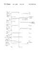
- the array architecture associated with the memory deviceis shown in FIG. 1 .
- the arraycontains N individual page buffers 105 in each bank of page buffers 101 , 102 ; thus, as there are both an upper 101 and lower 102 bank of page buffers, one entire page or word line 106 contains 2N bits.
- Left 103 and right 104 banks of decodersare used to select a particular word line.
- any numbers presented hereare merely illustrative of the principle of the invention as a whole. Those ordinarily skilled in the art will appreciate that the numbers associated with any of these elements, as well as the number of core memory cells in the overall device, may be changed without departing from the spirit and scope of the invention.
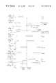
- FIG. 2shows the architecture of one core cell block 107 in the NAND-based flash memory device of FIG. 1 along with the associated page buffer 105 .
- the core cell block 107comprises 16 individual memory elements 120 - 136 and two select gates, SG 1 110 and SG 2 111 , for example.
- non-volatile transistorsembody the memory elements 120 - 136 and select gates 110 , 111 .
- the word lines 151 - 167 and select gate lines 150 , 168are connected with the control gates of the memory elements 120 - 136 and select gates 110 , 111 .
- the memory elements 120 - 136 and select gatesare connected in series. Specifically, the source and drain of the memory elements 120 - 136 are connected to each other in series.
- the source of the first memory element 120is tied to the drain of the second memory element 121
- the source of the second memory element 121is tied to the drain of the third memory element 122 , etc.
- the select gates 110 , 111are connected to the ends of the chain of memory elements 120 - 136 .
- the source of SG 1 110is connected with the drain of the first memory element 120
- the drain of SG 1 110is connected with a bitline 180
- the drain of SG 2 111is connected with the source of the last memory cell 136 and the source of SG 2 111 is connected with the array common voltage Vss 199 .
- the core cell block 107is connected with a page buffer 105 via a bitline 180 .
- the page buffer 105includes a sensing node 210 , a high voltage control transistor (CNTRL) 220 , an optional protection transistor (PROT) 230 , a transistor for discharging the bitline 205 , an isolation transistor 215 , and other necessary circuitry 270 well known in the art.
- the other circuitry 270may include, for example, a latch 280 for latching data onto and out of the bitline 180 , input/output circuitry for transferring data to the external system and assorted supporting circuitry inherent in the other circuitry 270 .
- the isolation transistor 215isolates the bitline 180 from the necessary circuitry 270 during specific operations and the discharging transistor 205 is used to discharge the bitline 180 when necessary.
- the PROT transistor 230is a high voltage n-channel transistor used for protecting the circuitry in the page buffer 105 and the memory circuitry in the core cell block 107 .
- the PROT transistor 230is optional, depending on the specific circuit design.
- the page buffer 105in addition comprises a prebias (pBIAS) transistor 250 .
- the pBIAS transistor 250is connected with the CNTRL transistor 220 such that the drain of CNTRL 220 is connected with the drain of pBIAS 250 , with the SNS node 210 located between the two transistors.
- the source of pBIAS 250is connected with the supply voltage Vcc 290 , and the source of CNTRL 220 is connected with the bitline 180 .
- the pBIAS transistor 250is a p-channel transistor, unlike the majority of the other transistors and memory elements in the core cell block 107 and page buffer 105 , which are n-channel transistors.
- the pBIAS transistor 250allows the bitline 180 to charge up to a preset voltage prior to detection of the output voltage at the sensing node 210 and also provides the sensing current.
- the page buffer circuitry 105comprises an additional n-channel transistor, the PRESET transistor 260 is provided for timing purposes.
- the n-channel PRESET transistor 260herein the PRESET transistor, is operational to ground one node of the latch 280 isolated by the isolation transistor 215 .
- the PRESET transistor 260is activated during the precharging cycle so that the latch 280 is set to a known state before sensing begins.
- the addition of the PRESET transistor 260is necessary for purposes of timing of signals associated with external elements of the flash memory device.
- FIGS. 3A, 3 B and 3 CIndividual memory elements can undergo three distinct operations, which are shown in FIGS. 3A, 3 B and 3 C.
- the three operationsare Program, shown in FIG. 3A, Erase, shown in FIG. 3B, and Read, shown in FIG. 3C, and are described below.
- Programshown in FIG. 3A
- Eraseshown in FIG. 3B
- Readshown in FIG. 3C
- This discussionwill be limited to standard, n-channel, NAND-based non-volatile memory elements, although those ordinarily skilled in the art will appreciate that the basic operations described herein can be easily extended to at least NOR-based non-volatile memory elements and bi-level non-volatile memory elements in which 4 states can be programmed.
- the structure of the memory element 300is well known in the art: a p-type semiconductor well 325 is disposed within a n-type semiconductor well 315 .
- the n-type semiconductor well 315is contained within a p-type semiconductor substrate 305 .
- a set of n-type semiconductor junctions comprising the source 310 and drain 320are disposed within the p-type semiconductor well 325 .
- the p-type semiconductor well 325 and n-type semiconductor well 315are usually maintained at the same voltage during device operation to avoid current flow from one of the well regions to the other.
- the memory elementfurther includes a control gate 330 and a floating gate 340 .
- the gates 330 , 340are conventionally formed from polysilicon deposited and patterned on the surface of the substrate, although the floating gate 340 may alternately be formed from an ONO layer.
- the gates 330 , 340are formed such that an oxide is formed on part of the substrate with the floating gate 340 formed above the oxide.
- the control gate 330is formed above the floating gate 340 and isolated from the floating gate 340 by a second oxide. Control signals are applied to the control gate 330 .
- both the source 310 and the drain 320 of the memory element 300are connected with Vss (usually ground).
- Vssusually ground
- the threshold voltage (or turn-on voltage) of the MOSFETis generally designed to be a negative voltage, so that a channel 350 of electrons 360 exists in the p-type semiconductor well 325 when the gate 330 is grounded.
- the channel 350is disposed between the source 310 and drain 320 of the memory element 300 .
- a large positive voltageis applied to the control gate 330 , which causes electrons 360 to be trapped onto the floating gate 340 via Fowler-Nordheim tunneling.
- the threshold voltage of the transistoris increased if electrons are trapped on the floating gate 340 . In this case, the threshold voltage of the programmed memory element changes from a negative voltage to a positive voltage.
- the source 310 and the drain 320 of the memory element 300are left floating while the control gate 330 is grounded at Vss.
- a large positive voltageis applied to both the p-type semiconductor well 325 and the n-type semiconductor well 315 .
- the electrons 360 trapped on the floating gate 340enter the p-type semiconductor well 325 via Fowler-Nordheim tunneling.
- the threshold voltagethus reverts to the original, unprogrammed threshold voltage of the transistor.
- the source 310 of the memory element 300is connected with Vss while the drain is connected with the bitline 180 .
- the voltage applied to the control gate 330 of the memory element 300is between the threshold voltage of memory elements that have been erased and memory elements that have been programmed. In this case, the threshold voltage of a programmed memory element is positive and that of an erased memory element is negative and thus applying Vss to the control gate 330 is sufficient to differentiate between the two states.
- the voltage or currentis determined at a sense node 210 on the bitline 180 to ascertain the state of the particular memory element selected, either programmed ( 0 ) or erased ( 1 ).
- the preferred embodiment to sensing a specific word lineis to charge the bitline before the specific word line is addressed.
- the bitlineis initially charged up to a value close to a predetermined sensing level and then isolated or left floating.
- Each word lineis connected with the control gate of a unique memory element in each core memory cell.
- all of the word line voltages not being tested and the select gate voltagesare held at a high enough voltage level to turn the memory element on or open the channel of the transistor.
- the applied voltagemust be greater than the voltage necessary to turn on a programmed memory element, whose threshold voltage is large, as well as an erased memory element, whose threshold voltage is substantially smaller.
- the voltage applied along the specific word line of the memory element to be readmust be between the voltage necessary to read an erased memory cell and that necessary to read a programmed memory cell. If the specific memory cell being read has been erased, when the test voltage is applied, a complete circuit from the bitline to ground is created and the bitline discharges. After a specific amount of time, the voltage on the bitline is read at the sensing node (SNS). At this time, if the voltage at the SNS node is approximately the original sensing level, 1.0 V for example, then the circuit connecting the bitline to ground was not completed and the memory cell has been programmed.
- SNSsensing node
- charge stored in the floating gate of the memory celltranslates to a high voltage at the sensing node on the bitline and corresponds to a logic value of 0.
- a low voltage at the sensing node on the bitlinecorresponds to a logic value of 1.
- FIGS. 4 A-IThe timing diagrams for the precharging mechanism having the precharging scheme of the first embodiment are shown in FIGS. 4 A-I. All input signals are applied to the control gate of transistors and memory elements. Prior to activation of the precharging and subsequent sensing/evaluation of the output signal at the SNS node, the voltage on the PRESET transistor 260 is approximately Vss. The voltage at the SNS node 210 and applied to the CNTRL 220 , PROT 230 , SG 1 110 , SG 2 111 transistors and all word lines 150 - 168 are also set to Vss. The voltage applied to the pBIAS transistor 250 is set to approximately Vcc.
- the precharging sequencestarts at time Tpc.
- Vccis applied to the PRESET transistor 260 and the voltage applied to pBIAS 250 decreases to a predetermined voltage, turning on the p-channel pBIAS transistor 250 .
- the pBIAS transistor 250is biased over the precharging time such that it sources a current that is approximately 2-3 times that of the normal current in the bitline during sensing, the normal current in the bitline being 2 ⁇ A, for example. This increase in current allows the bitline to charge to the preset sensing voltage faster without increasing the current/voltage requirements of the chip severely.
- the voltage applied to the CNTRL transistor 220is increased to maintain the voltage at the SNS node 210 at the sensing level of approximately 1.0 V. As the charge on the bitline increases, the CNTRL transistor 220 clamps the voltage at the SNS node 210 at the sensing voltage level.
- the voltage applied to the PROT transistor 230if the PROT transistor 230 is present, is brought to at least Vcc during the precharge cycle.
- All word line voltages applied to the individual memory elements in the core cell block 107are increased at Tpc.
- the non-read word line voltagesare subsequently maintained throughout the entire precharge cycle and evaluation phase at a voltage large enough to turn the transistors on, whether or not they have been individually programmed.
- the voltage applied to the select gate transistors SG 1 110 and SG 2 111 during the precharge cycleare different. As shown in FIGS. 4E and 4F, the voltage applied to SG 1 110 is large enough to turn the transistor on, while the voltage applied to SG 2 111 remains constant at Vss. In this embodiment, the SNS node 210 charges to the original sensing level of approximately 1.0 V prior to the sensing/evaluation phase.
- the evaluation phaseoccurs after the precharging cycle, at time Tsense.
- the voltages supplied to the transistors in the page buffer 105are modified at Tsense.
- the voltage applied to the PRESET transistor 260is decreased to Vss and the voltage applied to the pBIAS transistor 250 is increased such that the pBIAS transistor 250 sources the original sensing (non-precharging) current in the bitline.
- the voltage applied to the CNTRL transistor 220remains constant to keep the SNS node 210 at the sensing voltage and the voltage applied to the PROT transistor 230 remains at Vcc so that the PROT transistor 230 is on, if the PROT transistor 230 is present.
- the voltage applied to the SG 2 111 transistoris increased such that the transistor is turned on.
- the voltage on the word line to be readis set at an intermediate level, in which the state of the floating gate determines whether or not the transistor is turned on.
- the inputsdo not affect the voltage on the bitline until sensing begins. Little current flows through the core memory cell as the path to ground through the NAND chain is highly resistive. Thus, SG 2 111 effectively decouples the inputs from ground when the select gate is not activated.
- FIGS. 5 A-Ishow the timing diagrams associated with the pseudo-precharge scheme.
- the main difference between the pseudo-precharge scheme and the strict precharge schemeis the timing of the voltages applied to the select gate transistors SG 1 110 and SG 2 111 .
- both SG 1 110 and SG 2 111turn on at the same time, Tpc, the time at which the PRESET 260 signal is high.
- the word lines of the memory cells that are not readare increasing so that the transistors are turning on at the same time and the pBlAS transistor 250 again sources 2-3 times the normal sensing current, as in the strict precharging scheme.
- the voltage of the word line to be readis maintained at Vss. If the specific memory cell has been erased, a path is created between the bitline 180 and ground and thus, the memory cell sinks current. In this case, the bitline 180 does not get charged all the way to the normal sensing voltage and consequently, sensing occurs at a lower voltage and higher current.
- the new sensing voltage at SNS 210may be only 600 mV, instead of the original sensing voltage of 1.0 V.
- the sensing timeis decreased as the sensing voltage under the pseudo-precharge scheme is decreased.
- the inventionconsists of a precharging mechanism and schemes for precharging the data lines of the memory cells of NAND-based flash devices. Modifications are made to the page buffers associated with the core cell blocks comprising the overall memory section of the flash memory device. The modifications necessary to effect the invention include both additional circuit elements and changes in the timing of signals applied to elements within both core cell blocks and page buffers.
Landscapes
- Engineering & Computer Science (AREA)
- Microelectronics & Electronic Packaging (AREA)
- Read Only Memory (AREA)
Abstract
Description
Claims (18)
Priority Applications (1)
| Application Number | Priority Date | Filing Date | Title |
|---|---|---|---|
| US09/433,187US6175523B1 (en) | 1999-10-25 | 1999-10-25 | Precharging mechanism and method for NAND-based flash memory devices |
Applications Claiming Priority (1)
| Application Number | Priority Date | Filing Date | Title |
|---|---|---|---|
| US09/433,187US6175523B1 (en) | 1999-10-25 | 1999-10-25 | Precharging mechanism and method for NAND-based flash memory devices |
Publications (1)
| Publication Number | Publication Date |
|---|---|
| US6175523B1true US6175523B1 (en) | 2001-01-16 |
Family
ID=23719171
Family Applications (1)
| Application Number | Title | Priority Date | Filing Date |
|---|---|---|---|
| US09/433,187Expired - LifetimeUS6175523B1 (en) | 1999-10-25 | 1999-10-25 | Precharging mechanism and method for NAND-based flash memory devices |
Country Status (1)
| Country | Link |
|---|---|
| US (1) | US6175523B1 (en) |
Cited By (73)
| Publication number | Priority date | Publication date | Assignee | Title |
|---|---|---|---|---|
| US6396741B1 (en) | 2000-05-04 | 2002-05-28 | Saifun Semiconductors Ltd. | Programming of nonvolatile memory cells |
| US20030039153A1 (en)* | 2001-01-18 | 2003-02-27 | Eduardo Maayan | EEPROM array and method for operation thereof |
| US20030142544A1 (en)* | 2002-01-31 | 2003-07-31 | Eduardo Maayan | Mass storage array and methods for operation thereof |
| US20030235075A1 (en)* | 2002-06-21 | 2003-12-25 | Micron Technology, Inc. | Vertical NROM having a storage density of 1bit per 1F2 |
| US20040008541A1 (en)* | 2002-07-10 | 2004-01-15 | Eduardo Maayan | Multiple use memory chip |
| US20040022113A1 (en)* | 2002-08-01 | 2004-02-05 | Ran Dvir | High voltage insertion in flash memory cards |
| US20040130934A1 (en)* | 2002-06-21 | 2004-07-08 | Micron Technology, Inc. | NROM memory cell, memory array, related devices and methods |
| US20040190338A1 (en)* | 2003-03-28 | 2004-09-30 | Hynix Semiconductor Inc. | Structure for testing NAND flash memory and method of testing NAND flash memory |
| US20040222437A1 (en)* | 2000-12-07 | 2004-11-11 | Dror Avni | Programming and erasing methods for an NROM array |
| US6830963B1 (en) | 2003-10-09 | 2004-12-14 | Micron Technology, Inc. | Fully depleted silicon-on-insulator CMOS logic |
| US20040265011A1 (en)* | 2003-06-30 | 2004-12-30 | Kiyonori Tsuda | Powder transport apparatus and image forming apparatus that can stabilize replenishment of powder |
| US20050001229A1 (en)* | 2003-07-01 | 2005-01-06 | Leonard Forbes | Apparatus and method for split transistor memory having improved endurance |
| US20050030792A1 (en)* | 2003-08-07 | 2005-02-10 | Micron Technology, Inc. | Method for programming and erasing an nrom cell |
| US20050030794A1 (en)* | 2003-08-07 | 2005-02-10 | Micron Technology, Inc. | Method for erasing an NROM cell |
| US6878991B1 (en) | 2004-01-30 | 2005-04-12 | Micron Technology, Inc. | Vertical device 4F2 EEPROM memory |
| US20050106811A1 (en)* | 2003-11-17 | 2005-05-19 | Micron Technology, Inc. | NROM flash memory devices on ultrathin silicon |
| US20050105341A1 (en)* | 2003-11-04 | 2005-05-19 | Micron Technology, Inc. | NROM flash memory with self-aligned structural charge separation |
| US20050128804A1 (en)* | 2003-12-16 | 2005-06-16 | Micron Technology, Inc. | Multi-state NROM device |
| US20050138262A1 (en)* | 2003-12-18 | 2005-06-23 | Micron Technology, Inc. | Flash memory having a high-permittivity tunnel dielectric |
| US20050133860A1 (en)* | 2003-12-17 | 2005-06-23 | Micron Technology, Inc. | Vertical NROM NAND flash memory array |
| US20050173755A1 (en)* | 2004-02-10 | 2005-08-11 | Micron Technology, Inc. | NROM flash memory with a high-permittivity gate dielectric |
| US20050174847A1 (en)* | 2004-02-10 | 2005-08-11 | Micron Technology, Inc. | Nrom flash memory cell with integrated dram |
| US20050184337A1 (en)* | 2004-02-24 | 2005-08-25 | Micron Technology, Inc. | 4f2 eeprom nrom memory arrays with vertical devices |
| US20050185466A1 (en)* | 2004-02-24 | 2005-08-25 | Micron Technology, Inc. | Multi-state memory cell with asymmetric charge trapping |
| US20050212033A1 (en)* | 2004-03-24 | 2005-09-29 | Micron Technology, Inc. | Memory device with high dielectric constant gate dielectrics and metal floating gates |
| US20050247972A1 (en)* | 2004-05-06 | 2005-11-10 | Micron Technology, Inc. | Ballistic direct injection NROM cell on strained silicon structures |
| US20050253186A1 (en)* | 2003-09-05 | 2005-11-17 | Micron Technology, Inc. | Trench corner effect bidirectional flash memory cell |
| US6979857B2 (en) | 2003-07-01 | 2005-12-27 | Micron Technology, Inc. | Apparatus and method for split gate NROM memory |
| US20060036803A1 (en)* | 2004-08-16 | 2006-02-16 | Mori Edan | Non-volatile memory device controlled by a micro-controller |
| US20060083078A1 (en)* | 2004-10-15 | 2006-04-20 | Stmicroelectronics S.R.I. | Memory device |
| US20060083077A1 (en)* | 2004-10-15 | 2006-04-20 | Stmicroelectronics S.R.L. | Memory device |
| US20060128103A1 (en)* | 2003-12-16 | 2006-06-15 | Micron Technology, Inc. | NROM memory cell, memory array, related devices and methods |
| US20060126396A1 (en)* | 2002-01-31 | 2006-06-15 | Saifun Semiconductors, Ltd. | Method, system, and circuit for operating a non-volatile memory array |
| US20060146624A1 (en)* | 2004-12-02 | 2006-07-06 | Saifun Semiconductors, Ltd. | Current folding sense amplifier |
| US20060158940A1 (en)* | 2005-01-19 | 2006-07-20 | Saifun Semiconductors, Ltd. | Partial erase verify |
| US20060211188A1 (en)* | 2004-10-14 | 2006-09-21 | Saifun Semiconductors Ltd. | Non-volatile memory structure and method of fabrication |
| US20060250847A1 (en)* | 2005-04-11 | 2006-11-09 | Stmicroelectronics S.R.L. | Electronic non-volatile memory device having a cNAND structure and being monolithically integrated on semiconductor |
| US20060262598A1 (en)* | 1997-08-01 | 2006-11-23 | Saifun Semiconductors Ltd. | Two bit non-volatile electrically erasable and programmable semiconductor memory cell utilizing asymmetrical charge trapping |
| US20060285402A1 (en)* | 2004-03-29 | 2006-12-21 | Saifun Semiconductors Ltd. | Apparatus and methods for multi-level sensing in a memory array |
| US20070032016A1 (en)* | 2001-11-19 | 2007-02-08 | Saifun Semiconductors Ltd. | Protective layer in memory device and method therefor |
| US20070051982A1 (en)* | 2005-07-18 | 2007-03-08 | Saifun Semiconductors Ltd. | Dense non-volatile memory array and method of fabrication |
| US20070061498A1 (en)* | 2005-09-12 | 2007-03-15 | Huey-Tyug Chua | Method and System for NAND-Flash Identification without Reading Device ID Table |
| US20070096199A1 (en)* | 2005-09-08 | 2007-05-03 | Eli Lusky | Method of manufacturing symmetric arrays |
| US7221138B2 (en) | 2005-09-27 | 2007-05-22 | Saifun Semiconductors Ltd | Method and apparatus for measuring charge pump output current |
| US20070130439A1 (en)* | 2005-12-01 | 2007-06-07 | Sony Ericsson Mobile Communications Ab | Secure digital certificate storing scheme for flash memory and electronic apparatus |
| US20070133276A1 (en)* | 2003-09-16 | 2007-06-14 | Eli Lusky | Operating array cells with matched reference cells |
| US20070153575A1 (en)* | 2006-01-03 | 2007-07-05 | Saifun Semiconductors, Ltd. | Method, system, and circuit for operating a non-volatile memory array |
| US20070159880A1 (en)* | 2006-01-12 | 2007-07-12 | Boaz Eitan | Secondary injection for NROM |
| US20070168637A1 (en)* | 2003-01-31 | 2007-07-19 | Yan Polansky | Memory array programming circuit and a method for using the circuit |
| US20070171717A1 (en)* | 2004-08-12 | 2007-07-26 | Saifun Semiconductors Ltd. | Dynamic matching of signal path and reference path for sensing |
| US20070173017A1 (en)* | 2006-01-20 | 2007-07-26 | Saifun Semiconductors, Ltd. | Advanced non-volatile memory array and method of fabrication thereof |
| US20070196982A1 (en)* | 2006-02-21 | 2007-08-23 | Saifun Semiconductors Ltd. | Nrom non-volatile mode of operation |
| US20070194835A1 (en)* | 2006-02-21 | 2007-08-23 | Alexander Kushnarenko | Circuit and method for powering up an integrated circuit and an integrated circuit utilizing same |
| US20070195607A1 (en)* | 2006-02-21 | 2007-08-23 | Saifun Semiconductors Ltd. | Nrom non-volatile memory and mode of operation |
| US20070253248A1 (en)* | 2006-04-27 | 2007-11-01 | Eduardo Maayan | Method for programming a reference cell |
| US20070255889A1 (en)* | 2006-03-22 | 2007-11-01 | Yoav Yogev | Non-volatile memory device and method of operating the device |
| US7317633B2 (en) | 2004-07-06 | 2008-01-08 | Saifun Semiconductors Ltd | Protection of NROM devices from charge damage |
| US20080013379A1 (en)* | 2006-07-14 | 2008-01-17 | Macronix International Co., Ltd. | Method and apparatus for reading data from nonvolatile memory |
| US20080094127A1 (en)* | 2006-09-18 | 2008-04-24 | Yoram Betser | Measuring and controlling current consumption and output current of charge pumps |
| US20080239599A1 (en)* | 2007-04-01 | 2008-10-02 | Yehuda Yizraeli | Clamping Voltage Events Such As ESD |
| US7512009B2 (en) | 2001-04-05 | 2009-03-31 | Saifun Semiconductors Ltd. | Method for programming a reference cell |
| US7535765B2 (en) | 2004-12-09 | 2009-05-19 | Saifun Semiconductors Ltd. | Non-volatile memory device and method for reading cells |
| US20090201747A1 (en)* | 2008-02-07 | 2009-08-13 | Macronix International Co., Ltd. | Memory, bit-line pre-charge circuit and bit-line pre-charge method |
| US7638835B2 (en) | 2006-02-28 | 2009-12-29 | Saifun Semiconductors Ltd. | Double density NROM with nitride strips (DDNS) |
| US7668017B2 (en) | 2005-08-17 | 2010-02-23 | Saifun Semiconductors Ltd. | Method of erasing non-volatile memory cells |
| US7675782B2 (en) | 2002-10-29 | 2010-03-09 | Saifun Semiconductors Ltd. | Method, system and circuit for programming a non-volatile memory array |
| US20100302868A1 (en)* | 2009-05-29 | 2010-12-02 | Jung Chul Han | Method of operating nonvolatile memory device |
| US8053812B2 (en) | 2005-03-17 | 2011-11-08 | Spansion Israel Ltd | Contact in planar NROM technology |
| TWI409817B (en)* | 2009-04-20 | 2013-09-21 | Winbond Electronics Corp | Data output module and sensing circuit for flash memory |
| US9761310B2 (en) | 2014-09-06 | 2017-09-12 | NEO Semiconductor, Inc. | Method and apparatus for storing information using a memory able to perform both NVM and DRAM functions |
| US10242743B2 (en) | 2014-09-06 | 2019-03-26 | NEO Semiconductor, Inc. | Method and apparatus for writing nonvolatile memory using multiple-page programming |
| US10720215B2 (en) | 2014-09-06 | 2020-07-21 | Fu-Chang Hsu | Methods and apparatus for writing nonvolatile 3D NAND flash memory using multiple-page programming |
| USRE50025E1 (en)* | 2007-09-14 | 2024-06-25 | Kioxia Corporation | Non-volatile semiconductor memory device including application of different voltages to memory cells based on their proximity to a selected memory cell |
Citations (14)
| Publication number | Priority date | Publication date | Assignee | Title |
|---|---|---|---|---|
| US4173766A (en) | 1977-09-16 | 1979-11-06 | Fairchild Camera And Instrument Corporation | Insulated gate field-effect transistor read-only memory cell |
| GB2157489A (en) | 1984-03-23 | 1985-10-23 | Hitachi Ltd | A semiconductor integrated circuit memory device |
| US5280446A (en) | 1990-09-20 | 1994-01-18 | Bright Microelectronics, Inc. | Flash eprom memory circuit having source side programming |
| US5349221A (en) | 1991-10-25 | 1994-09-20 | Rohm Co., Ltd. | Semiconductor memory device and method of reading out information for the same |
| US5748529A (en)* | 1995-11-15 | 1998-05-05 | Samsung Electronics Co., Ltd. | Integrated circuit memory devices having direct read capability |
| US5748536A (en)* | 1995-05-27 | 1998-05-05 | Samsung Electronics Co., Ltd. | Data read circuit for a nonvolatile semiconductor memory |
| US5768192A (en) | 1996-07-23 | 1998-06-16 | Saifun Semiconductors, Ltd. | Non-volatile semiconductor memory cell utilizing asymmetrical charge trapping |
| US5825686A (en) | 1995-02-16 | 1998-10-20 | Siemens Aktiengesellschaft | Multi-value read-only memory cell having an improved signal-to-noise ratio |
| US5847998A (en) | 1996-12-20 | 1998-12-08 | Advanced Micro Devices, Inc. | Non-volatile memory array that enables simultaneous read and write operations |
| US5867430A (en) | 1996-12-20 | 1999-02-02 | Advanced Micro Devices Inc | Bank architecture for a non-volatile memory enabling simultaneous reading and writing |
| WO1999007000A2 (en) | 1997-08-01 | 1999-02-11 | Saifun Semiconductors Ltd. | Two bit eeprom using asymmetrical charge trapping |
| US5986929A (en)* | 1997-05-22 | 1999-11-16 | Kabushiki Kaisha Toshiba | Multi-level nonvolatile semiconductor memory device |
| US6055188A (en)* | 1997-04-30 | 2000-04-25 | Kabushiki Kaishi Toshiba | Nonvolatile semiconductor memory device having a data circuit for erasing and writing operations |
| US6058042A (en)* | 1997-12-26 | 2000-05-02 | Sony Corporation | Semiconductor nonvolatile memory device and method of data programming the same |
- 1999
- 1999-10-25USUS09/433,187patent/US6175523B1/ennot_activeExpired - Lifetime
Patent Citations (14)
| Publication number | Priority date | Publication date | Assignee | Title |
|---|---|---|---|---|
| US4173766A (en) | 1977-09-16 | 1979-11-06 | Fairchild Camera And Instrument Corporation | Insulated gate field-effect transistor read-only memory cell |
| GB2157489A (en) | 1984-03-23 | 1985-10-23 | Hitachi Ltd | A semiconductor integrated circuit memory device |
| US5280446A (en) | 1990-09-20 | 1994-01-18 | Bright Microelectronics, Inc. | Flash eprom memory circuit having source side programming |
| US5349221A (en) | 1991-10-25 | 1994-09-20 | Rohm Co., Ltd. | Semiconductor memory device and method of reading out information for the same |
| US5825686A (en) | 1995-02-16 | 1998-10-20 | Siemens Aktiengesellschaft | Multi-value read-only memory cell having an improved signal-to-noise ratio |
| US5748536A (en)* | 1995-05-27 | 1998-05-05 | Samsung Electronics Co., Ltd. | Data read circuit for a nonvolatile semiconductor memory |
| US5748529A (en)* | 1995-11-15 | 1998-05-05 | Samsung Electronics Co., Ltd. | Integrated circuit memory devices having direct read capability |
| US5768192A (en) | 1996-07-23 | 1998-06-16 | Saifun Semiconductors, Ltd. | Non-volatile semiconductor memory cell utilizing asymmetrical charge trapping |
| US5847998A (en) | 1996-12-20 | 1998-12-08 | Advanced Micro Devices, Inc. | Non-volatile memory array that enables simultaneous read and write operations |
| US5867430A (en) | 1996-12-20 | 1999-02-02 | Advanced Micro Devices Inc | Bank architecture for a non-volatile memory enabling simultaneous reading and writing |
| US6055188A (en)* | 1997-04-30 | 2000-04-25 | Kabushiki Kaishi Toshiba | Nonvolatile semiconductor memory device having a data circuit for erasing and writing operations |
| US5986929A (en)* | 1997-05-22 | 1999-11-16 | Kabushiki Kaisha Toshiba | Multi-level nonvolatile semiconductor memory device |
| WO1999007000A2 (en) | 1997-08-01 | 1999-02-11 | Saifun Semiconductors Ltd. | Two bit eeprom using asymmetrical charge trapping |
| US6058042A (en)* | 1997-12-26 | 2000-05-02 | Sony Corporation | Semiconductor nonvolatile memory device and method of data programming the same |
Cited By (236)
| Publication number | Priority date | Publication date | Assignee | Title |
|---|---|---|---|---|
| US20060262598A1 (en)* | 1997-08-01 | 2006-11-23 | Saifun Semiconductors Ltd. | Two bit non-volatile electrically erasable and programmable semiconductor memory cell utilizing asymmetrical charge trapping |
| US20080111177A1 (en)* | 1997-08-01 | 2008-05-15 | Eduardo Maayan | Non-volatile memory cell and non-volatile memory device using said cell |
| US7405969B2 (en) | 1997-08-01 | 2008-07-29 | Saifun Semiconductors Ltd. | Non-volatile memory cell and non-volatile memory devices |
| US20090032862A1 (en)* | 1997-08-01 | 2009-02-05 | Eduardo Maayan | Non-volatile memory cell and non-volatile memory device using said cell |
| US6396741B1 (en) | 2000-05-04 | 2002-05-28 | Saifun Semiconductors Ltd. | Programming of nonvolatile memory cells |
| US20030072192A1 (en)* | 2000-05-04 | 2003-04-17 | Ilan Bloom | Programming of nonvolatile memory cells |
| US6937521B2 (en) | 2000-05-04 | 2005-08-30 | Saifun Semiconductors Ltd. | Programming and erasing methods for a non-volatile memory cell |
| US6829172B2 (en) | 2000-05-04 | 2004-12-07 | Saifun Semiconductors Ltd. | Programming of nonvolatile memory cells |
| US6928001B2 (en) | 2000-12-07 | 2005-08-09 | Saifun Semiconductors Ltd. | Programming and erasing methods for a non-volatile memory cell |
| US20040222437A1 (en)* | 2000-12-07 | 2004-11-11 | Dror Avni | Programming and erasing methods for an NROM array |
| US7518908B2 (en) | 2001-01-18 | 2009-04-14 | Saifun Semiconductors Ltd. | EEPROM array and method for operation thereof |
| US20030039153A1 (en)* | 2001-01-18 | 2003-02-27 | Eduardo Maayan | EEPROM array and method for operation thereof |
| US7512009B2 (en) | 2001-04-05 | 2009-03-31 | Saifun Semiconductors Ltd. | Method for programming a reference cell |
| US20070032016A1 (en)* | 2001-11-19 | 2007-02-08 | Saifun Semiconductors Ltd. | Protective layer in memory device and method therefor |
| US20060126396A1 (en)* | 2002-01-31 | 2006-06-15 | Saifun Semiconductors, Ltd. | Method, system, and circuit for operating a non-volatile memory array |
| US7420848B2 (en) | 2002-01-31 | 2008-09-02 | Saifun Semiconductors Ltd. | Method, system, and circuit for operating a non-volatile memory array |
| US20030142544A1 (en)* | 2002-01-31 | 2003-07-31 | Eduardo Maayan | Mass storage array and methods for operation thereof |
| US6975536B2 (en) | 2002-01-31 | 2005-12-13 | Saifun Semiconductors Ltd. | Mass storage array and methods for operation thereof |
| US6853587B2 (en) | 2002-06-21 | 2005-02-08 | Micron Technology, Inc. | Vertical NROM having a storage density of 1 bit per 1F2 |
| US20090010075A9 (en)* | 2002-06-21 | 2009-01-08 | Micron Technologies, Inc. | NROM memory cell, memory array, related devices and methods |
| US20060126398A1 (en)* | 2002-06-21 | 2006-06-15 | Micron Technologies, Inc. | NROM memory cell, memory array, related devices and methods |
| US20060124998A1 (en)* | 2002-06-21 | 2006-06-15 | Micron Technology, Inc. | NROM memory cell, memory array, related devices and methods |
| US20030235075A1 (en)* | 2002-06-21 | 2003-12-25 | Micron Technology, Inc. | Vertical NROM having a storage density of 1bit per 1F2 |
| US7541242B2 (en) | 2002-06-21 | 2009-06-02 | Micron Technology, Inc. | NROM memory cell, memory array, related devices and methods |
| US6842370B2 (en) | 2002-06-21 | 2005-01-11 | Micron Technology, Inc. | Vertical NROM having a storage density of 1 bit per 1F2 |
| US7230848B2 (en) | 2002-06-21 | 2007-06-12 | Micron Technology, Inc. | Vertical NROM having a storage density of 1 bit per 1F2 |
| US6906953B2 (en) | 2002-06-21 | 2005-06-14 | Micron Technology, Inc. | Vertical NROM having a storage density of 1 bit per 1F2 |
| US7535048B2 (en) | 2002-06-21 | 2009-05-19 | Micron Technology, Inc. | NROM memory cell, memory array, related devices and methods |
| US20050255647A1 (en)* | 2002-06-21 | 2005-11-17 | Micron Technology, Inc. | Vertical NROM having a storage density of 1 bit per 1F2 |
| US20040066672A1 (en)* | 2002-06-21 | 2004-04-08 | Micron Technology, Inc. | Vertical NROM having a storage density of 1 bit per IF2 |
| US20090072303A9 (en)* | 2002-06-21 | 2009-03-19 | Micron Technology, Inc. | Nrom memory cell, memory array, related devices and methods |
| US20040130934A1 (en)* | 2002-06-21 | 2004-07-08 | Micron Technology, Inc. | NROM memory cell, memory array, related devices and methods |
| US7220634B2 (en) | 2002-06-21 | 2007-05-22 | Micron Technology, Inc. | NROM memory cell, memory array, related devices and methods |
| US20040202032A1 (en)* | 2002-06-21 | 2004-10-14 | Micron Technology, Inc. | Vertical NROM having a storage density of 1 bit per 1F2 |
| US8441056B2 (en) | 2002-06-21 | 2013-05-14 | Micron Technology, Inc. | NROM memory cell, memory array, related devices and methods |
| US6917544B2 (en) | 2002-07-10 | 2005-07-12 | Saifun Semiconductors Ltd. | Multiple use memory chip |
| US20040008541A1 (en)* | 2002-07-10 | 2004-01-15 | Eduardo Maayan | Multiple use memory chip |
| US20060152975A1 (en)* | 2002-07-10 | 2006-07-13 | Eduardo Maayan | Multiple use memory chip |
| US7738304B2 (en) | 2002-07-10 | 2010-06-15 | Saifun Semiconductors Ltd. | Multiple use memory chip |
| US6826107B2 (en) | 2002-08-01 | 2004-11-30 | Saifun Semiconductors Ltd. | High voltage insertion in flash memory cards |
| US20040022113A1 (en)* | 2002-08-01 | 2004-02-05 | Ran Dvir | High voltage insertion in flash memory cards |
| US7675782B2 (en) | 2002-10-29 | 2010-03-09 | Saifun Semiconductors Ltd. | Method, system and circuit for programming a non-volatile memory array |
| US7743230B2 (en) | 2003-01-31 | 2010-06-22 | Saifun Semiconductors Ltd. | Memory array programming circuit and a method for using the circuit |
| US20070168637A1 (en)* | 2003-01-31 | 2007-07-19 | Yan Polansky | Memory array programming circuit and a method for using the circuit |
| US20060120154A1 (en)* | 2003-03-28 | 2006-06-08 | Hynix Semiconductor Inc. | Structure for testing nand flash memory and method of testing nand flash memory |
| US20040190338A1 (en)* | 2003-03-28 | 2004-09-30 | Hynix Semiconductor Inc. | Structure for testing NAND flash memory and method of testing NAND flash memory |
| US7031190B2 (en)* | 2003-03-28 | 2006-04-18 | Hynix Semiconductor Inc. | Structure for testing NAND flash memory and method of testing NAND flash memory |
| US7391663B2 (en) | 2003-03-28 | 2008-06-24 | Hynix Semiconductor Inc. | Structure and method for measuring the channel boosting voltage of NAND flash memory at a node between drain/source select transistor and adjacent flash memory cell |
| US20040265011A1 (en)* | 2003-06-30 | 2004-12-30 | Kiyonori Tsuda | Powder transport apparatus and image forming apparatus that can stabilize replenishment of powder |
| US7095075B2 (en) | 2003-07-01 | 2006-08-22 | Micron Technology, Inc. | Apparatus and method for split transistor memory having improved endurance |
| US20050001229A1 (en)* | 2003-07-01 | 2005-01-06 | Leonard Forbes | Apparatus and method for split transistor memory having improved endurance |
| US7719046B2 (en) | 2003-07-01 | 2010-05-18 | Micron Technology, Inc. | Apparatus and method for trench transistor memory having different gate dielectric thickness |
| US20060197143A1 (en)* | 2003-07-01 | 2006-09-07 | Micron Technology, Inc. | Apparatus and method for split transistor memory having improved endurance |
| US6979857B2 (en) | 2003-07-01 | 2005-12-27 | Micron Technology, Inc. | Apparatus and method for split gate NROM memory |
| US20050141278A1 (en)* | 2003-08-07 | 2005-06-30 | Micron Technology, Inc. | Method for programming and erasing an NROM cell |
| US7639530B2 (en) | 2003-08-07 | 2009-12-29 | Micron Technology, Inc. | Method for programming and erasing an NROM cell |
| US7075831B2 (en) | 2003-08-07 | 2006-07-11 | Micron Technology, Inc. | Method for erasing an NROM cell |
| US7088619B2 (en) | 2003-08-07 | 2006-08-08 | Micron Technology, Inc. | Method for programming and erasing an NROM cell |
| US7272045B2 (en) | 2003-08-07 | 2007-09-18 | Micron Technology, Inc. | Method for programming and erasing an NROM cell |
| US7075832B2 (en) | 2003-08-07 | 2006-07-11 | Micron Technology, Inc. | Method for erasing an NROM cell |
| US20050174855A1 (en)* | 2003-08-07 | 2005-08-11 | Micron Technology, Inc. | Method for erasing an NROM cell |
| US20050030792A1 (en)* | 2003-08-07 | 2005-02-10 | Micron Technology, Inc. | Method for programming and erasing an nrom cell |
| US7986555B2 (en) | 2003-08-07 | 2011-07-26 | Micron Technology, Inc. | Method for programming and erasing an NROM cell |
| US7085170B2 (en) | 2003-08-07 | 2006-08-01 | Micron Technology, Ind. | Method for erasing an NROM cell |
| US7277321B2 (en) | 2003-08-07 | 2007-10-02 | Micron Technology, Inc. | Method for programming and erasing an NROM cell |
| US6873550B2 (en) | 2003-08-07 | 2005-03-29 | Micron Technology, Inc. | Method for programming and erasing an NROM cell |
| US20070064466A1 (en)* | 2003-08-07 | 2007-03-22 | Micron Technology, Inc. | Method for programming and erasing an NROM cell |
| US20100067307A1 (en)* | 2003-08-07 | 2010-03-18 | Micron Technology, Inc. | Method for programming and erasing an nrom cell |
| US7227787B2 (en) | 2003-08-07 | 2007-06-05 | Micron Technology, Inc. | Method for erasing an NROM cell |
| US20050030794A1 (en)* | 2003-08-07 | 2005-02-10 | Micron Technology, Inc. | Method for erasing an NROM cell |
| US20060133152A1 (en)* | 2003-08-07 | 2006-06-22 | Micron Technology, Inc. | Method for programming and erasing an NROM cell |
| US7161217B2 (en) | 2003-09-05 | 2007-01-09 | Micron Technology, Inc. | Trench corner effect bidirectional flash memory cell |
| US6977412B2 (en) | 2003-09-05 | 2005-12-20 | Micron Technology, Inc. | Trench corner effect bidirectional flash memory cell |
| US20050258480A1 (en)* | 2003-09-05 | 2005-11-24 | Micron Technology, Inc. | Trench corner effect bidirectional flash memory cell |
| US7285821B2 (en) | 2003-09-05 | 2007-10-23 | Micron Technology, Inc. | Trench corner effect bidirectional flash memory cell |
| US7329920B2 (en) | 2003-09-05 | 2008-02-12 | Micron Technology, Inc. | Trench corner effect bidirectional flash memory cell |
| US20050253186A1 (en)* | 2003-09-05 | 2005-11-17 | Micron Technology, Inc. | Trench corner effect bidirectional flash memory cell |
| US20050255638A1 (en)* | 2003-09-05 | 2005-11-17 | Micron Technology, Inc. | Trench corner effect bidirectional flash memory cell |
| US20050269625A1 (en)* | 2003-09-05 | 2005-12-08 | Micron Technology, Inc. | Trench corner effect bidirectional flash memory cell |
| US7535054B2 (en) | 2003-09-05 | 2009-05-19 | Micron Technology, Inc. | Trench corner effect bidirectional flash memory cell |
| US7283394B2 (en) | 2003-09-05 | 2007-10-16 | Micron Technology, Inc. | Trench corner effect bidirectional flash memory cell |
| US20070133276A1 (en)* | 2003-09-16 | 2007-06-14 | Eli Lusky | Operating array cells with matched reference cells |
| US7457183B2 (en) | 2003-09-16 | 2008-11-25 | Saifun Semiconductors Ltd. | Operating array cells with matched reference cells |
| US8174081B2 (en) | 2003-10-09 | 2012-05-08 | Micron Technology, Inc. | Fully depleted silicon-on-insulator CMOS logic |
| US20110204431A1 (en)* | 2003-10-09 | 2011-08-25 | Micron Technology, Inc. | Fully depleted silicon-on-insulator cmos logic |
| US7078770B2 (en) | 2003-10-09 | 2006-07-18 | Micron Technology, Inc. | Fully depleted silicon-on-insulator CMOS logic |
| US7973370B2 (en) | 2003-10-09 | 2011-07-05 | Micron Technology, Inc. | Fully depleted silicon-on-insulator CMOS logic |
| US20050077564A1 (en)* | 2003-10-09 | 2005-04-14 | Micron Technology, Inc. | Fully depleted silicon-on-insulator CMOS logic |
| US6830963B1 (en) | 2003-10-09 | 2004-12-14 | Micron Technology, Inc. | Fully depleted silicon-on-insulator CMOS logic |
| US7480186B2 (en) | 2003-11-04 | 2009-01-20 | Micron Technology, Inc. | NROM flash memory with self-aligned structural charge separation |
| US7184315B2 (en) | 2003-11-04 | 2007-02-27 | Micron Technology, Inc. | NROM flash memory with self-aligned structural charge separation |
| US20070109871A1 (en)* | 2003-11-04 | 2007-05-17 | Micron Technology, Inc. | NROM flash memory with self-aligned structural charge separation |
| US20050105341A1 (en)* | 2003-11-04 | 2005-05-19 | Micron Technology, Inc. | NROM flash memory with self-aligned structural charge separation |
| US20100270610A1 (en)* | 2003-11-17 | 2010-10-28 | Micron Technology, Inc. | Nrom flash memory devices on ultrathin silicon |
| US20070170496A1 (en)* | 2003-11-17 | 2007-07-26 | Micron Technology, Inc. | Nrom flash memory devices on ultrathin silicon |
| US7276762B2 (en) | 2003-11-17 | 2007-10-02 | Micron Technology, Inc. | NROM flash memory devices on ultrathin silicon |
| US7915669B2 (en) | 2003-11-17 | 2011-03-29 | Micron Technology, Inc. | NROM flash memory devices on ultrathin silicon |
| US7276413B2 (en) | 2003-11-17 | 2007-10-02 | Micron Technology, Inc. | NROM flash memory devices on ultrathin silicon |
| US7358562B2 (en) | 2003-11-17 | 2008-04-15 | Micron Technology, Inc. | NROM flash memory devices on ultrathin silicon |
| US20070166927A1 (en)* | 2003-11-17 | 2007-07-19 | Micron Technology, Inc. | Nrom flash memory devices on ultrathin silicon |
| US7244987B2 (en) | 2003-11-17 | 2007-07-17 | Micron Technology, Inc. | NROM flash memory devices on ultrathin silicon |
| US20050106811A1 (en)* | 2003-11-17 | 2005-05-19 | Micron Technology, Inc. | NROM flash memory devices on ultrathin silicon |
| US20110163321A1 (en)* | 2003-11-17 | 2011-07-07 | Micron Technology, Inc. | Nrom flash memory devices on ultrathin silicon |
| US7768058B2 (en) | 2003-11-17 | 2010-08-03 | Micron Technology, Inc. | NROM flash memory devices on ultrathin silicon |
| US20050280094A1 (en)* | 2003-11-17 | 2005-12-22 | Micron Technology, Inc. | NROM flash memory devices on ultrathin silicon |
| US7378316B2 (en) | 2003-11-17 | 2008-05-27 | Micron Technology, Inc. | Method for fabricating semiconductor vertical NROM memory cells |
| US20050280089A1 (en)* | 2003-11-17 | 2005-12-22 | Micron Technology, Inc. | NROM flash memory devices on ultrathin silicon |
| US20050282334A1 (en)* | 2003-11-17 | 2005-12-22 | Micron Technology, Inc. | NROM flash memory devices on ultrathin silicon |
| US7202523B2 (en) | 2003-11-17 | 2007-04-10 | Micron Technology, Inc. | NROM flash memory devices on ultrathin silicon |
| US8183625B2 (en) | 2003-11-17 | 2012-05-22 | Micron Technology, Inc. | NROM flash memory devices on ultrathin silicon |
| US20080203467A1 (en)* | 2003-11-17 | 2008-08-28 | Micron Technology, Inc. | Nrom flash memory devices on ultrathin silicon |
| US7371642B2 (en) | 2003-12-16 | 2008-05-13 | Micron Technology, Inc. | Multi-state NROM device |
| US20060128103A1 (en)* | 2003-12-16 | 2006-06-15 | Micron Technology, Inc. | NROM memory cell, memory array, related devices and methods |
| US20060124992A1 (en)* | 2003-12-16 | 2006-06-15 | Micron Technology, Inc. | NROM memory cell, memory array, related devices and methods |
| US20060124967A1 (en)* | 2003-12-16 | 2006-06-15 | Micron Technology, Inc. | NROM memory cell, memory array, related devices and methods |
| US20060152978A1 (en)* | 2003-12-16 | 2006-07-13 | Micron Technology, Inc. | Multi-state NROM device |
| US7050330B2 (en) | 2003-12-16 | 2006-05-23 | Micron Technology, Inc. | Multi-state NROM device |
| US7750389B2 (en) | 2003-12-16 | 2010-07-06 | Micron Technology, Inc. | NROM memory cell, memory array, related devices and methods |
| US7238599B2 (en) | 2003-12-16 | 2007-07-03 | Micron Technology, Inc. | Multi-state NROM device |
| US20060166443A1 (en)* | 2003-12-16 | 2006-07-27 | Micron Technology, Inc. | Multi-state NROM device |
| US7269072B2 (en) | 2003-12-16 | 2007-09-11 | Micron Technology, Inc. | NROM memory cell, memory array, related devices and methods |
| US20060128104A1 (en)* | 2003-12-16 | 2006-06-15 | Micron Technology, Inc. | NROM memory cell, memory array, related devices and methods |
| US7301804B2 (en) | 2003-12-16 | 2007-11-27 | Micro Technology, Inc. | NROM memory cell, memory array, related devices and methods |
| US7269071B2 (en) | 2003-12-16 | 2007-09-11 | Micron Technology, Inc. | NROM memory cell, memory array, related devices and methods |
| US20050128804A1 (en)* | 2003-12-16 | 2005-06-16 | Micron Technology, Inc. | Multi-state NROM device |
| US7241654B2 (en) | 2003-12-17 | 2007-07-10 | Micron Technology, Inc. | Vertical NROM NAND flash memory array |
| US20050133860A1 (en)* | 2003-12-17 | 2005-06-23 | Micron Technology, Inc. | Vertical NROM NAND flash memory array |
| US20060261404A1 (en)* | 2003-12-17 | 2006-11-23 | Micron Technology, Inc. | Vertical NROM NAND flash memory array |
| US7339239B2 (en) | 2003-12-17 | 2008-03-04 | Micron Technology, Inc. | Vertical NROM NAND flash memory array |
| US20090191676A1 (en)* | 2003-12-18 | 2009-07-30 | Micron Technology, Inc. | Flash memory having a high-permittivity tunnel dielectric |
| US7157769B2 (en) | 2003-12-18 | 2007-01-02 | Micron Technology, Inc. | Flash memory having a high-permittivity tunnel dielectric |
| US20050138262A1 (en)* | 2003-12-18 | 2005-06-23 | Micron Technology, Inc. | Flash memory having a high-permittivity tunnel dielectric |
| US7528037B2 (en) | 2003-12-18 | 2009-05-05 | Micron Technology, Inc. | Flash memory having a high-permittivity tunnel dielectric |
| US20050277243A1 (en)* | 2003-12-18 | 2005-12-15 | Micron Technology, Inc. | Flash memory having a high-permittivity tunnel dielectric |
| US6878991B1 (en) | 2004-01-30 | 2005-04-12 | Micron Technology, Inc. | Vertical device 4F2 EEPROM memory |
| US7157771B2 (en) | 2004-01-30 | 2007-01-02 | Micron Technology, Inc. | Vertical device 4F2 EEPROM memory |
| US7332773B2 (en) | 2004-01-30 | 2008-02-19 | Micron Technology, Inc. | Vertical device 4F2 EEPROM memory |
| US20050167743A1 (en)* | 2004-01-30 | 2005-08-04 | Micron Technology, Inc. | Vertical device 4F2 EEPROM memory |
| US20060261405A1 (en)* | 2004-01-30 | 2006-11-23 | Micron Technology, Inc. | Vertical device 4F² eeprom memory |
| US20060019453A1 (en)* | 2004-02-10 | 2006-01-26 | Micron Technology, Inc. | NROM flash memory with a high-permittivity gate dielectric |
| US6952366B2 (en) | 2004-02-10 | 2005-10-04 | Micron Technology, Inc. | NROM flash memory cell with integrated DRAM |
| US20050173755A1 (en)* | 2004-02-10 | 2005-08-11 | Micron Technology, Inc. | NROM flash memory with a high-permittivity gate dielectric |
| US20050174847A1 (en)* | 2004-02-10 | 2005-08-11 | Micron Technology, Inc. | Nrom flash memory cell with integrated dram |
| US7479428B2 (en) | 2004-02-10 | 2009-01-20 | Leonard Forbes | NROM flash memory with a high-permittivity gate dielectric |
| US7221018B2 (en) | 2004-02-10 | 2007-05-22 | Micron Technology, Inc. | NROM flash memory with a high-permittivity gate dielectric |
| US7072213B2 (en) | 2004-02-10 | 2006-07-04 | Micron Technology, Inc. | NROM flash memory cell with integrated DRAM |
| US7319613B2 (en) | 2004-02-10 | 2008-01-15 | Micron Technology, Inc. | NROM flash memory cell with integrated DRAM |
| US20050275011A1 (en)* | 2004-02-10 | 2005-12-15 | Micron Technology, Inc. | NROM flash memory with a high-permittivity gate dielectric |
| US20050240867A1 (en)* | 2004-02-10 | 2005-10-27 | Micron Technology, Inc. | NROM flash memory cell with integrated DRAM |
| US20050185466A1 (en)* | 2004-02-24 | 2005-08-25 | Micron Technology, Inc. | Multi-state memory cell with asymmetric charge trapping |
| US7616482B2 (en) | 2004-02-24 | 2009-11-10 | Micron Technology, Inc. | Multi-state memory cell with asymmetric charge trapping |
| US7911837B2 (en) | 2004-02-24 | 2011-03-22 | Micron Technology, Inc. | Multi-state memory cell with asymmetric charge trapping |
| US7282762B2 (en) | 2004-02-24 | 2007-10-16 | Micron Technology, Inc. | 4F2 EEPROM NROM memory arrays with vertical devices |
| US20050184337A1 (en)* | 2004-02-24 | 2005-08-25 | Micron Technology, Inc. | 4f2 eeprom nrom memory arrays with vertical devices |
| US20060203554A1 (en)* | 2004-02-24 | 2006-09-14 | Micron Technology, Inc. | Multi-state memory cell with asymmetric charge trapping |
| US20060203555A1 (en)* | 2004-02-24 | 2006-09-14 | Micron Technology, Inc. | Multi-state memory cell with asymmetric charge trapping |
| US7072217B2 (en) | 2004-02-24 | 2006-07-04 | Micron Technology, Inc. | Multi-state memory cell with asymmetric charge trapping |
| US20100039869A1 (en)* | 2004-02-24 | 2010-02-18 | Micron Technology, Inc. | Multi-state memory cell with asymmetric charge trapping |
| US7075146B2 (en) | 2004-02-24 | 2006-07-11 | Micron Technology, Inc. | 4F2 EEPROM NROM memory arrays with vertical devices |
| US7577027B2 (en) | 2004-02-24 | 2009-08-18 | Micron Technology, Inc. | Multi-state memory cell with asymmetric charge trapping |
| US8076714B2 (en) | 2004-03-24 | 2011-12-13 | Micron Technology, Inc. | Memory device with high dielectric constant gate dielectrics and metal floating gates |
| US7268031B2 (en) | 2004-03-24 | 2007-09-11 | Micron Technology, Inc. | Memory device with high dielectric constant gate dielectrics and metal floating gates |
| US7586144B2 (en) | 2004-03-24 | 2009-09-08 | Micron Technology, Inc. | Memory device with high dielectric constant gate dielectrics and metal floating gates |
| US20090294830A1 (en)* | 2004-03-24 | 2009-12-03 | Micron Technology, Inc. | Memory device with high dielectric constant gate dielectrics and metal floating gates |
| US7550339B2 (en) | 2004-03-24 | 2009-06-23 | Micron Technology, Inc. | Memory device with high dielectric constant gate dielectrics and metal floating gates |
| US7102191B2 (en) | 2004-03-24 | 2006-09-05 | Micron Technologies, Inc. | Memory device with high dielectric constant gate dielectrics and metal floating gates |
| US20050212033A1 (en)* | 2004-03-24 | 2005-09-29 | Micron Technology, Inc. | Memory device with high dielectric constant gate dielectrics and metal floating gates |
| US20050280048A1 (en)* | 2004-03-24 | 2005-12-22 | Micron Technology, Inc. | Memory device with high dielectric constant gate dielectrics and metal floating gates |
| US20060237775A1 (en)* | 2004-03-24 | 2006-10-26 | Micron Technology, Inc. | Memory device with high dielectric constant gate dielectrics and metal floating gates |
| US7532529B2 (en) | 2004-03-29 | 2009-05-12 | Saifun Semiconductors Ltd. | Apparatus and methods for multi-level sensing in a memory array |
| US20060285402A1 (en)* | 2004-03-29 | 2006-12-21 | Saifun Semiconductors Ltd. | Apparatus and methods for multi-level sensing in a memory array |
| US7859046B2 (en) | 2004-05-06 | 2010-12-28 | Micron Technology, Inc. | Ballistic direct injection NROM cell on strained silicon structures |
| US7274068B2 (en) | 2004-05-06 | 2007-09-25 | Micron Technology, Inc. | Ballistic direct injection NROM cell on strained silicon structures |
| US20060214220A1 (en)* | 2004-05-06 | 2006-09-28 | Micron Technology, Inc. | Ballistic direct injection NROM cell on strained silicon structures |
| US7683424B2 (en) | 2004-05-06 | 2010-03-23 | Micron Technology, Inc. | Ballistic direct injection NROM cell on strained silicon structures |
| US20050247972A1 (en)* | 2004-05-06 | 2005-11-10 | Micron Technology, Inc. | Ballistic direct injection NROM cell on strained silicon structures |
| US7317633B2 (en) | 2004-07-06 | 2008-01-08 | Saifun Semiconductors Ltd | Protection of NROM devices from charge damage |
| US20070171717A1 (en)* | 2004-08-12 | 2007-07-26 | Saifun Semiconductors Ltd. | Dynamic matching of signal path and reference path for sensing |
| US7466594B2 (en) | 2004-08-12 | 2008-12-16 | Saifun Semiconductors Ltd. | Dynamic matching of signal path and reference path for sensing |
| US20060036803A1 (en)* | 2004-08-16 | 2006-02-16 | Mori Edan | Non-volatile memory device controlled by a micro-controller |
| US20100173464A1 (en)* | 2004-10-14 | 2010-07-08 | Eli Lusky | Non-volatile memory structure and method of fabrication |
| US20060211188A1 (en)* | 2004-10-14 | 2006-09-21 | Saifun Semiconductors Ltd. | Non-volatile memory structure and method of fabrication |
| US7964459B2 (en) | 2004-10-14 | 2011-06-21 | Spansion Israel Ltd. | Non-volatile memory structure and method of fabrication |
| US7638850B2 (en) | 2004-10-14 | 2009-12-29 | Saifun Semiconductors Ltd. | Non-volatile memory structure and method of fabrication |
| US7196943B2 (en) | 2004-10-15 | 2007-03-27 | Stmicroelectronics S.R.L. | Memory device |
| US7352645B2 (en) | 2004-10-15 | 2008-04-01 | Stmicroelectronics S.R.L. | Memory device |
| US20060083078A1 (en)* | 2004-10-15 | 2006-04-20 | Stmicroelectronics S.R.I. | Memory device |
| US20060083077A1 (en)* | 2004-10-15 | 2006-04-20 | Stmicroelectronics S.R.L. | Memory device |
| US20060146624A1 (en)* | 2004-12-02 | 2006-07-06 | Saifun Semiconductors, Ltd. | Current folding sense amplifier |
| US7535765B2 (en) | 2004-12-09 | 2009-05-19 | Saifun Semiconductors Ltd. | Non-volatile memory device and method for reading cells |
| US20060158940A1 (en)* | 2005-01-19 | 2006-07-20 | Saifun Semiconductors, Ltd. | Partial erase verify |
| US7369440B2 (en) | 2005-01-19 | 2008-05-06 | Saifun Semiconductors Ltd. | Method, circuit and systems for erasing one or more non-volatile memory cells |
| US7468926B2 (en) | 2005-01-19 | 2008-12-23 | Saifun Semiconductors Ltd. | Partial erase verify |
| US8053812B2 (en) | 2005-03-17 | 2011-11-08 | Spansion Israel Ltd | Contact in planar NROM technology |
| US7675788B2 (en)* | 2005-04-11 | 2010-03-09 | Giovanni Campardo | Electronic non-volatile memory device having a cNAND structure and being monolithically integrated on semiconductor |
| US20060250847A1 (en)* | 2005-04-11 | 2006-11-09 | Stmicroelectronics S.R.L. | Electronic non-volatile memory device having a cNAND structure and being monolithically integrated on semiconductor |
| US20070051982A1 (en)* | 2005-07-18 | 2007-03-08 | Saifun Semiconductors Ltd. | Dense non-volatile memory array and method of fabrication |
| US7786512B2 (en) | 2005-07-18 | 2010-08-31 | Saifun Semiconductors Ltd. | Dense non-volatile memory array and method of fabrication |
| US7668017B2 (en) | 2005-08-17 | 2010-02-23 | Saifun Semiconductors Ltd. | Method of erasing non-volatile memory cells |
| US20070096199A1 (en)* | 2005-09-08 | 2007-05-03 | Eli Lusky | Method of manufacturing symmetric arrays |
| US8429326B2 (en) | 2005-09-12 | 2013-04-23 | Mediatek Inc. | Method and system for NAND-flash identification without reading device ID table |
| US20070061498A1 (en)* | 2005-09-12 | 2007-03-15 | Huey-Tyug Chua | Method and System for NAND-Flash Identification without Reading Device ID Table |
| US7221138B2 (en) | 2005-09-27 | 2007-05-22 | Saifun Semiconductors Ltd | Method and apparatus for measuring charge pump output current |
| US20070130439A1 (en)* | 2005-12-01 | 2007-06-07 | Sony Ericsson Mobile Communications Ab | Secure digital certificate storing scheme for flash memory and electronic apparatus |
| US8195945B2 (en)* | 2005-12-01 | 2012-06-05 | Sony Mobile Communications Ab | Secure digital certificate storing scheme for flash memory and electronic apparatus |
| US7352627B2 (en) | 2006-01-03 | 2008-04-01 | Saifon Semiconductors Ltd. | Method, system, and circuit for operating a non-volatile memory array |
| US20070153575A1 (en)* | 2006-01-03 | 2007-07-05 | Saifun Semiconductors, Ltd. | Method, system, and circuit for operating a non-volatile memory array |
| US20070159880A1 (en)* | 2006-01-12 | 2007-07-12 | Boaz Eitan | Secondary injection for NROM |
| US7808818B2 (en) | 2006-01-12 | 2010-10-05 | Saifun Semiconductors Ltd. | Secondary injection for NROM |
| US20070173017A1 (en)* | 2006-01-20 | 2007-07-26 | Saifun Semiconductors, Ltd. | Advanced non-volatile memory array and method of fabrication thereof |
| US7692961B2 (en) | 2006-02-21 | 2010-04-06 | Saifun Semiconductors Ltd. | Method, circuit and device for disturb-control of programming nonvolatile memory cells by hot-hole injection (HHI) and by channel hot-electron (CHE) injection |
| US7760554B2 (en) | 2006-02-21 | 2010-07-20 | Saifun Semiconductors Ltd. | NROM non-volatile memory and mode of operation |
| US20070196982A1 (en)* | 2006-02-21 | 2007-08-23 | Saifun Semiconductors Ltd. | Nrom non-volatile mode of operation |
| US8253452B2 (en) | 2006-02-21 | 2012-08-28 | Spansion Israel Ltd | Circuit and method for powering up an integrated circuit and an integrated circuit utilizing same |
| US20070194835A1 (en)* | 2006-02-21 | 2007-08-23 | Alexander Kushnarenko | Circuit and method for powering up an integrated circuit and an integrated circuit utilizing same |
| US20070195607A1 (en)* | 2006-02-21 | 2007-08-23 | Saifun Semiconductors Ltd. | Nrom non-volatile memory and mode of operation |
| US7638835B2 (en) | 2006-02-28 | 2009-12-29 | Saifun Semiconductors Ltd. | Double density NROM with nitride strips (DDNS) |
| US20070255889A1 (en)* | 2006-03-22 | 2007-11-01 | Yoav Yogev | Non-volatile memory device and method of operating the device |
| US7701779B2 (en) | 2006-04-27 | 2010-04-20 | Sajfun Semiconductors Ltd. | Method for programming a reference cell |
| US20070253248A1 (en)* | 2006-04-27 | 2007-11-01 | Eduardo Maayan | Method for programming a reference cell |
| US7339846B2 (en) | 2006-07-14 | 2008-03-04 | Macronix International Co., Ltd. | Method and apparatus for reading data from nonvolatile memory |
| US20080013379A1 (en)* | 2006-07-14 | 2008-01-17 | Macronix International Co., Ltd. | Method and apparatus for reading data from nonvolatile memory |
| US7605579B2 (en) | 2006-09-18 | 2009-10-20 | Saifun Semiconductors Ltd. | Measuring and controlling current consumption and output current of charge pumps |
| US20080094127A1 (en)* | 2006-09-18 | 2008-04-24 | Yoram Betser | Measuring and controlling current consumption and output current of charge pumps |
| US20080239599A1 (en)* | 2007-04-01 | 2008-10-02 | Yehuda Yizraeli | Clamping Voltage Events Such As ESD |
| USRE50025E1 (en)* | 2007-09-14 | 2024-06-25 | Kioxia Corporation | Non-volatile semiconductor memory device including application of different voltages to memory cells based on their proximity to a selected memory cell |
| US7586802B2 (en)* | 2008-02-07 | 2009-09-08 | Macronix International Co. Ltd. | Memory, bit-line pre-charge circuit and bit-line pre-charge method |
| CN101504862B (en)* | 2008-02-07 | 2012-05-23 | 旺宏电子股份有限公司 | Storage device, bit line precharging circuit and bit line precharging method |
| US20090201747A1 (en)* | 2008-02-07 | 2009-08-13 | Macronix International Co., Ltd. | Memory, bit-line pre-charge circuit and bit-line pre-charge method |
| TWI409817B (en)* | 2009-04-20 | 2013-09-21 | Winbond Electronics Corp | Data output module and sensing circuit for flash memory |
| US8174903B2 (en)* | 2009-05-29 | 2012-05-08 | Hynix Semiconductor Inc. | Method of operating nonvolatile memory device |
| US20100302868A1 (en)* | 2009-05-29 | 2010-12-02 | Jung Chul Han | Method of operating nonvolatile memory device |
| US9761310B2 (en) | 2014-09-06 | 2017-09-12 | NEO Semiconductor, Inc. | Method and apparatus for storing information using a memory able to perform both NVM and DRAM functions |
| US10163509B2 (en) | 2014-09-06 | 2018-12-25 | NEO Semiconductor, Inc. | Method and apparatus for storing information using a memory able to perform both NVM and DRAM functions |
| US10242743B2 (en) | 2014-09-06 | 2019-03-26 | NEO Semiconductor, Inc. | Method and apparatus for writing nonvolatile memory using multiple-page programming |
| US10720215B2 (en) | 2014-09-06 | 2020-07-21 | Fu-Chang Hsu | Methods and apparatus for writing nonvolatile 3D NAND flash memory using multiple-page programming |
Similar Documents
| Publication | Publication Date | Title |
|---|---|---|
| US6175523B1 (en) | Precharging mechanism and method for NAND-based flash memory devices | |
| US6240020B1 (en) | Method of bitline shielding in conjunction with a precharging scheme for nand-based flash memory devices | |
| US7573752B2 (en) | NAND flash memory cell programming | |
| US6717857B2 (en) | Non-volatile semiconductor memory device with cache function and program, read, and page copy-back operations thereof | |
| US5511022A (en) | Depletion mode NAND string electrically erasable programmable semiconductor memory device and method for erasing and programming thereof | |
| KR100347866B1 (en) | Nand flash memory device | |
| US5973962A (en) | Method of programming non-volatile memory devices having a NAND type cell array | |
| US7164608B2 (en) | NVRAM memory cell architecture that integrates conventional SRAM and flash cells | |
| US5790456A (en) | Multiple bits-per-cell flash EEPROM memory cells with wide program and erase Vt window | |
| US7539059B2 (en) | Selective bit line precharging in non volatile memory | |
| US6310809B1 (en) | Adjustable pre-charge in a memory | |
| US20060193174A1 (en) | Non-volatile and static random access memory cells sharing the same bitlines | |
| JP2000149581A (en) | Non-volatile semiconductor memory | |
| US8400840B2 (en) | NAND memory device and programming methods | |
| US6359821B1 (en) | Differential sensing in a memory with reference current | |
| US5402382A (en) | Nonvolatile semiconductor memory device capable of erasing by a word line unit | |
| US5515327A (en) | Nonvolatile semiconductor memory device having a small number of internal boosting circuits | |
| US6714453B2 (en) | Flash memory including means of checking memory cell threshold voltages | |
| US6859392B2 (en) | Preconditioning global bitlines | |
| US5070480A (en) | Nonvolatile associative memory system | |
| US6567314B1 (en) | Data programming implementation for high efficiency CHE injection | |
| WO1997005623A1 (en) | Flash memory system having reduced disturb and method | |
| US5831901A (en) | Method of programming a memory cell to contain multiple values | |
| KR100634456B1 (en) | Flash memory device and its reading method | |
| US6496434B1 (en) | Differential sensing in a memory using two cycle pre-charge |
Legal Events
| Date | Code | Title | Description |
|---|---|---|---|
| AS | Assignment | Owner name:ADVANCED MIRCO DEVICES, INC., CALIFORNIA Free format text:ASSIGNMENT OF ASSIGNORS INTEREST;ASSIGNORS:YANG, ANDREW;HOLLMER, SHANE;LEE, BINH Q.;REEL/FRAME:010553/0125;SIGNING DATES FROM 19991020 TO 19991026 | |
| AS | Assignment | Owner name:ADVANCED MICRO DEVICES, INC., CALIFORNIA Free format text:CORRECTIVE ASSIGNMENT TO CORRECT THE RECEIVING PARTY, PREVIOUSLY RECORDED AT REEL 010553 FRAME 0125;ASSIGNORS:YANG, ANDREW;HOLLMER, SHANE;LEE, BINH Q.;REEL/FRAME:011248/0986;SIGNING DATES FROM 19991020 TO 20001026 | |
| STCF | Information on status: patent grant | Free format text:PATENTED CASE | |
| FEPP | Fee payment procedure | Free format text:PAYOR NUMBER ASSIGNED (ORIGINAL EVENT CODE: ASPN); ENTITY STATUS OF PATENT OWNER: LARGE ENTITY | |
| FPAY | Fee payment | Year of fee payment:4 | |
| AS | Assignment | Owner name:SPANSION INC., CALIFORNIA Free format text:ASSIGNMENT OF ASSIGNORS INTEREST;ASSIGNOR:ADVANCED MICRO DEVICES, INC.;REEL/FRAME:019047/0482 Effective date:20070131 | |
| AS | Assignment | Owner name:SPANSION LLC, CALIFORNIA Free format text:ASSIGNMENT OF ASSIGNORS INTEREST;ASSIGNOR:SPANSION INC.;REEL/FRAME:019069/0141 Effective date:20070131 | |
| FPAY | Fee payment | Year of fee payment:8 | |
| AS | Assignment | Owner name:BARCLAYS BANK PLC,NEW YORK Free format text:SECURITY AGREEMENT;ASSIGNORS:SPANSION LLC;SPANSION INC.;SPANSION TECHNOLOGY INC.;AND OTHERS;REEL/FRAME:024522/0338 Effective date:20100510 Owner name:BARCLAYS BANK PLC, NEW YORK Free format text:SECURITY AGREEMENT;ASSIGNORS:SPANSION LLC;SPANSION INC.;SPANSION TECHNOLOGY INC.;AND OTHERS;REEL/FRAME:024522/0338 Effective date:20100510 | |
| FPAY | Fee payment | Year of fee payment:12 | |
| AS | Assignment | Owner name:SPANSION TECHNOLOGY LLC, CALIFORNIA Free format text:RELEASE OF LIEN ON PATENT;ASSIGNOR:BARCLAYS BANK PLC;REEL/FRAME:030945/0505 Effective date:20130805 Owner name:SPANSION INC., CALIFORNIA Free format text:RELEASE OF LIEN ON PATENT;ASSIGNOR:BARCLAYS BANK PLC;REEL/FRAME:030945/0505 Effective date:20130805 Owner name:SPANSION TECHNOLOGY INC., CALIFORNIA Free format text:RELEASE OF LIEN ON PATENT;ASSIGNOR:BARCLAYS BANK PLC;REEL/FRAME:030945/0505 Effective date:20130805 Owner name:SPANSION LLC, CALIFORNIA Free format text:RELEASE OF LIEN ON PATENT;ASSIGNOR:BARCLAYS BANK PLC;REEL/FRAME:030945/0505 Effective date:20130805 | |
| AS | Assignment | Owner name:VALLEY DEVICE MANAGEMENT, DELAWARE Free format text:ASSIGNMENT OF ASSIGNORS INTEREST;ASSIGNOR:SPANSION LLC;REEL/FRAME:036011/0839 Effective date:20130731 |