US6175417B1 - Method and apparatus for detecting defects in the manufacture of an electronic device - Google Patents
Method and apparatus for detecting defects in the manufacture of an electronic deviceDownload PDFInfo
- Publication number
- US6175417B1 US6175417B1US09/532,869US53286900AUS6175417B1US 6175417 B1US6175417 B1US 6175417B1US 53286900 AUS53286900 AUS 53286900AUS 6175417 B1US6175417 B1US 6175417B1
- Authority
- US
- United States
- Prior art keywords
- image
- processor
- measurement
- sem
- detected
- Prior art date
- Legal status (The legal status is an assumption and is not a legal conclusion. Google has not performed a legal analysis and makes no representation as to the accuracy of the status listed.)
- Expired - Lifetime
Links
Images


Classifications
- G—PHYSICS
- G01—MEASURING; TESTING
- G01N—INVESTIGATING OR ANALYSING MATERIALS BY DETERMINING THEIR CHEMICAL OR PHYSICAL PROPERTIES
- G01N21/00—Investigating or analysing materials by the use of optical means, i.e. using sub-millimetre waves, infrared, visible or ultraviolet light
- G01N21/84—Systems specially adapted for particular applications
- G01N21/88—Investigating the presence of flaws or contamination
- G01N21/95—Investigating the presence of flaws or contamination characterised by the material or shape of the object to be examined
- G01N21/956—Inspecting patterns on the surface of objects
- G01N21/95684—Patterns showing highly reflecting parts, e.g. metallic elements
- Y—GENERAL TAGGING OF NEW TECHNOLOGICAL DEVELOPMENTS; GENERAL TAGGING OF CROSS-SECTIONAL TECHNOLOGIES SPANNING OVER SEVERAL SECTIONS OF THE IPC; TECHNICAL SUBJECTS COVERED BY FORMER USPC CROSS-REFERENCE ART COLLECTIONS [XRACs] AND DIGESTS
- Y10—TECHNICAL SUBJECTS COVERED BY FORMER USPC
- Y10S—TECHNICAL SUBJECTS COVERED BY FORMER USPC CROSS-REFERENCE ART COLLECTIONS [XRACs] AND DIGESTS
- Y10S977/00—Nanotechnology
- Y10S977/70—Nanostructure
- Y10S977/773—Nanoparticle, i.e. structure having three dimensions of 100 nm or less
Definitions
- the inventionis directed to the field of fabricating and manufacturing electronic devices. More specifically, the invention is directed to a measurement and detection method and apparatus for detecting defects in the manufacture of an electronic device such as a semiconductor integrated circuit or a wafer composed of a plurality of integrated circuits.
- Automated systemsincrease the process efficiency and reliability as the machines performing the inspection are more consistent than human operators who vary in ability and experience and are subject to fatigue when performing repetitive tasks.
- the automated systemsalso provide greater amounts of data regarding the production and equipment, which enables process engineers to both better analyze and control the process.
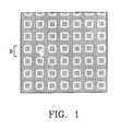
- Pattern inspectionOne such automated inspection step is known as “pattern inspection.” Many different “patterns” appear on both the wafer and the masks used to produce the ICs. Patterns may be repeated areas on a single IC such as test areas, memory areas, shift registers, adders, etc., or, as shown in FIG. 1, the ICs (or dies) themselves may be considered a “pattern” that is repeated throughout the wafer.
- Typical pattern inspection systemsare image based, as described, for example, in U.S. Pat. Nos. 4,794,646; 5,057,689; 5,641,960; and 5,659,172.
- the wafer, or part thereofis scanned and a highly resolved picture or image of the pertinent “pattern” is obtained.
- This pattern imageis compared to other pattern images retrieved from the same or other wafers, or is compared to an ideal image stored in the inspection system database. Differences highlighted in this comparison identify possible defects in the IC or wafer.
- CD measurementAnother inspection step that is typically automated in processes today is known as “critical dimension (CD) measurement.”
- CD featuresinclude transistor channel length (gate length), transistor channel width, trench depth, step slope, spacing, contact dimensions, etc.
- gate lengthgate length
- step slopestep slope
- spacingcontact dimensions
- CD measurementcan be done during several different stages in the fabrication process (e.g., masking, developing, final inspection, etc.).
- the ability of a viewing system to distinguish detailis related to the wavelength of the light (radiation) used. The shorter the wavelength, the smaller the detail that can be seen. With feature sizes breaking the sub-micron barrier, it is imperative that variations in the lower sub-micron range be detected. One error, even of this small magnitude, may be enough to render the entire IC or wafer useless. Only the SEM provides the capability to detect these variations.
- fiducial markers on wafersare typically included for the purpose of locating certain features or structures—usually test targets.
- U.S. Pat. No. 5,109,430discloses use of fine scale marks fabricated in a pattern in a two-dimensional array to form a target occupying a region of the IC where circuitry is not to be formed, e.g., between bonding pads or in a region interior to the bonding pads.
- Different patterns on different layerscan be used to detect misalignment between layers, as well as measure critical dimensions of the patterns.
- test targetsare specially designed structures included on the wafer for test purposes only. If the test targets are the correct size and shape, it follows that other semiconductor devices in their proximity will also have the correct size and shape and will therefore function properly.
- the CD-SEMcompares stored image data of the fiducial wafer markers with the scanned images received from the current position of the wafer under the CD-SEM. Once a “best match” is made, the CD-SEM is in correct position to perform the CD measurement on the intended “test target” for that particular location of the wafer (or IC).
- the inventionprovides a unique apparatus for and method of detecting defects in an electronic device.
- the electronic deviceis a semiconductor integrated circuit (IC), particularly one of a plurality of IC dies fabricated on a wafer of silicon or other semiconductor material.
- the defect detection operationis effectuated by a unique combination of critical dimension measurement and pattern inspection techniques.
- ICsemiconductor integrated circuit
- the defect detection operationis effectuated by a unique combination of critical dimension measurement and pattern inspection techniques.
- a “best fit” comparisonis made between a reference feature image and the currently scanned feature image.
- a “worst fit” comparisonis made between the reference feature image and the scanned feature images.
- a “worst fit” determinationrepresents pattern distortions or defects in the ICs under evaluation.
- the inventionthus provides a method and apparatus for detecting defects in an electronic device while scanning for the areas at which critical dimension measurements are to be made, thereby avoiding the need to carry out the otherwise separate steps of defect pattern recognition and CD measurement.
- FIG. 1illustrates patterns of integrated circuit dies formed on a silicon wafer
- FIG. 2is a schematic diagram of a SEM in accordance with a preferred embodiment of the invention.
- FIG. 3shows images captured by a SEM in accordance with a preferred embodiment of the invention
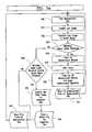
- FIGS. 4 a and 4 bare flowcharts describing the operation of preferred embodiments of the invention.
- FIGS. 5 a and 5 bare flowcharts describing the operation of additional preferred embodiments of the invention.
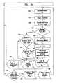
- FIGS. 6 a and 6 bare flowcharts describing the operation of yet additional preferred embodiments of the invention.
- FIG. 7is a block diagram of an apparatus in accordance with an preferred embodiment of the invention.
- a method and apparatus for detecting defects in the manufacture of an electronic device such as an integrated circuit (IC) on a silicon waferis provided.
- a defect detection stationas shown in FIG. 2, can be constructed having a scanning electron-beam microscope (SEM) 1 used for viewing purposes, as is well known in the art.
- SEMscanning electron-beam microscope
- the inventionis described herein as used during final wafer inspection of the IC dies, it can readily be appreciated that the invention has application to any other stage of manufacturing, e.g., inspection after the initial photomasking and baking of a wafer known as “development inspection,” where critical dimension measurements or pattern inspections are contemplated.
- SEM 1is provided with an object support structure 4 in the form of a stage or chuck, which may be moveable or stationary.
- An object 5 under evaluationsuch as an IC sample die or a wafer containing many IC dies rests on stage 4 .
- the stage 4may be moveable in two (X-Y) or three (X-Y-Z) dimensions to facilitate the proper viewing of object 5 (or parts thereof).
- a deflector 2 and detector 3are also provided within SEM 1 to assist in the viewing of object 5 .
- An image processor 7together with its accompanying image memory 7 a are provided to process the image signals output by SEM 1 and transform the signals into visual representations or data which can be viewed on a display monitor 8 (e.g., cathode ray tube (CRT)) or used for processing in computer 6 .
- a display monitor 8e.g., cathode ray tube (CRT)
- CRTcathode ray tube
- SEM 1uses a finely focused electron beam directed by deflector 2 , preferably under the control of computer 6 , to scan the surface of the object 5 resting on stage 4 , typically in two dimensions (X-Y).
- the object 5 under evaluationis a silicon wafer having a plurality of semiconductor integrated circuit dies fabricated thereon.
- the electrons striking the semiconductor surface of object 5collide with inner shell electrons of the object atoms causing inelastic collisions of low energy emitting so-called “secondary electrons” which are serially detected by detector 3 .
- the detected electron currentis output as an image signal to computer 6 and image processor 7 where an image representative of the surface of the object 5 can be formed based on the image signal.
- This imageis stored in image memory 7 a and can be viewed on monitor 8 or otherwise processed by computer 6 .
- the high resolution of the imageis attributed to the small diameter (e.g., several nanometers) of the electron beam illuminator.
- the visual contrast achieved in the imageoriginates mostly from variations in the extent of the secondary electron emissions from the topographic features of the surface of the object 5 .
- the defect detection stationincorporates within computer 6 a collection of modules such as central processing unit 60 , a window adjust unit 61 , a measurement site memory 62 , a CD measurement unit 63 , a database 64 , an image capture unit 65 , a SEM control unit 66 , an inspection site memory 67 , a pattern inspect unit 68 , and local bus 69 .
- modulesmay either be hardware components, software components, or a combination of hardware/software components constructed as known in the art to accomplish the functions described herein.
- the componentsmay be implemented individually or together as a single group (e.g., a single computer program run on a computer processor or the like such as CPU 60 ).
- the inventionmay be implemented in a conventional CD-SEM such as the “IVS-200” made by IVS, Inc., the “Opal 7830si” made by Applied Materials, or the “S-8820/8620” made by Hitachi, by modifying the computer program used by the control computer within the SEM such that the control computer implements in software the functions of each module described herein and the operations performed in the flowcharts of FIGS. 4 a through 6 b.
- CD measure 63 and pattern inspect 68may be combined with CPU 60
- measure site memory 62 and inspection site memory 67can be combined.
- the inventionIn detecting defects in the object 5 , the invention relies on a combination of pattern inspection and critical dimension measurement techniques. In particular, the invention relies on the use of a SEM, which performs critical dimension measurements, to perform the pattern inspection while the SEM is performing its function of CD measurement. As the SEM is searching for the “best match” image of a fiducial wafer marker, the SEM simultaneously searches for differences between stored reference patterns and the image patterns detected from the current wafer. Where the SEM detects a significant aberration in the current image pattern, as shown as pattern 44 b in FIG. 3 (as well as in region “D” on FIG. 1 ), the SEM determines that a defect has been found. As an alternative to the fiducial wafer markers, other CD features or other components of an IC or wafer may be used for measurement such as transistor channel length (gate length), transistor channel width, trench depth, step slope, spacing, contact dimensions, etc.
- FIGS. 4 a, 4 b, 5 a, 5 b, 6 a and 6 bwhich are executed, for example, by the SEM computer and with each representing a respective preferred embodiment of the invention.
- SEM control 66(FIG. 7) controls the deflector 2 and stage 4 to permit SEM 1 to scan one or more measurement sites of the wafer 5 (S 10 ).
- the measurement siteis preferably one of several different regions or sections of an IC die fabricated on the wafer 5 (although it may also be one of several sections of wafer 5 made up of a plurality of IC dies). As shown in FIG.
- each measurement site 40preferably contains a plurality of cells 44 a, 44 b in a semiconductor memory device.
- the sitesmay alternatively contain a plurality of circuit components or features of the IC, or they may even be a plurality of IC dies.
- “test target” regionsmay serve as measurement sites. “Test targets” are made up of non-functional structures that are fabricated in portions of the wafer or IC itself where no functional circuitry is placed, as described in U.S. Pat. No. 5,109,430, which is incorporated herein by reference in its entirety.
- SEM 1then initiates acquisition or capture (S 11 ) of a “live” image of the image area.
- the “live” imageis over a plurality of cells, e.g., 44 a, 44 b, etc. in a semiconductor memory, as shown in FIG. 3 .
- computer 1relies on detector 3 to sense the secondary electrons emitted from the area on wafer 5 .
- Image capture module 65takes control of the transmission of the image signal output from detector 3 to image processor 7 , as well as the storage of the “live” image, as represented by the image signal, in image memory 7 a.
- Central processing unit (CPU) 60retrieves a stored image 42 (FIG. 3) of a pattern or feature 42 that serves as the reference (or “ideal”) pattern that can be used as a template.
- the reference patternis an image of a semiconductor memory cell created based on design rules, etc. developed by manufacturing personnel and stored in database 64 (or some other storage device).
- the image 42may also be taken from a calibrating “reference” wafer, from other in-line wafers, or even from adjacent IC dies or measurement sites on the same wafer 5 , as can be recognized by those of ordinary skill in the art.
- CPU 60then performs in Step S 12 a comparison between all of the cells, including cells 44 a and 44 b, of the measurement site 40 and the reference cell 46 of stored image 42 to determine the similarities (or dissimilarities) between the individual measurement site cells such as 44 a and 44 b, and reference cell 46 , and to produce a comparison score reflecting the similarities/dissimilarities.
- Any known comparison algorithm or calculating devicemay be utilized to produce a comparison score that provides some indication of similarities/dissimilarities of the images.
- CPU 60may be programmed to calculate an image quotient by dividing the number of pixels found to be the same between the live and reference sites by the total number of pixels available.
- CPU 60uses the comparison score thus calculated to determine the “best fit” between each of the “live” measurement cell sites and the stored measurement site 46 .
- the “best fit”may be found by determining whether any the comparison scores for an individual measurement site under evaluation exceeds an upper threshold (S 13 ).
- the “best fit”may be found by determining whether the comparison score for an individual measurement site cell, e.g., 44 a, under evaluation exceeds an “upper threshold” value, which is preferably assigned by the operator, engineer, or designer and stored in the database 64 or other program memory prior to use on the manufacturing floor. (S 13 ).
- CPU 60will compare the image of an individual cell of measurement site 40 with the reference cell 46 of reference site 42 stored in database 64 . For each individual cell considered, CPU 60 will calculate a comparison score until CPU 60 detects a comparison score that exceeds the “upper threshold” value. The first time the “upper threshold” is exceeded based on one of the cells, e.g., 44 a, 44 b, CPU 60 will send an enable signal over local bus 69 to CD measure unit 63 , which is operative to perform a CD measurement on the feature or structure appearing at the current measurement site cell 44 a (S 13 ). If CPU 60 has compared all of the cells in measurement site 40 to the reference cell 46 and found that none of the calculated comparison scores exceed the “upper threshold” value (S 13 ), the process turns to step S 23 , which will be described later below.
- window adjust module 61places a CD measurement window around the current measurement site, e.g. 44 a (S 14 ).
- SEM control 66directs stage 4 to reposition wafer 5 and automatically focus (S 15 ) SEM 1 to permit CD measurements to be made, in a manner well known in the art.
- image capture module 65together with image processor 7 and image memory 7 a, the surface of the wafer 5 within the CD measurement window is scanned into image memory 7 a, and the CD measurements taken by CD measure unit 63 (S 16 ).
- CD measure unit 63may employ any CD measurement algorithm or technique known in the art to produce the dimensions or sizes of the measurement feature.
- the CD measurement data derivedis then stored in measurement site memory 62 (S 17 ).
- CPU 60next determines whether any of the above-calculated comparison scores falls below a “lower threshold” (S 18 ).
- CPU 60stores in an internal/external CPU memory (not shown), database 64 , or any other storage unit, the calculated comparison scores for each cell of the measurement site 40 being evaluated.
- step S 18CPU 60 reviews the stored comparison scores and determines which, if any, fall below the “lower threshold” value. In the case where comparison scores for all of the cells 44 a, 44 b were not calculated in step S 12 because a cell was reached which exceeded the upper threshold in step S 13 , CPU 60 proceeds to calculate the remainder of the comparison scores for the remainder of cells in measurement site 40 .
- the value assigned to the “lower threshold”is preferably predetermined prior to use on the manufacturing floor.
- CPU 60finds that any of the comparison scores falls below the “lower threshold,” CPU 60 directs image capture module 65 to capture the current “live” image 40 or, alternatively, only the image of the defective cell 44 b, and store the image in inspection site memory 67 (S 19 ). Subsequently, CPU 60 stores a defect flag corresponding to the defect detected in inspection site memory 67 (S 20 ). CPU 60 then causes the basic process flow to repeat for the next measurement site 40 (S 10 ).
- step S 18CPU 60 finds that none of the comparison scores fall below the “lower threshold” value for any of cells 44 a, 44 b, CPU 60 restarts the process again with the next measurement site (S 10 ).
- CPU 60in step S 13 , finds that none of the comparison scores exceed the “upper threshold” value, CPU 60 may cause an “error code” to be stored in measurement site memory 62 (S 23 ) associated with the measurement site 40 under evaluation. The process may then begin again with the next measurement site (S 10 ).
- the “upper threshold”may be dynamically assigned based on the relative comparison scores of other measurement site cells in the same live image 40 , or based on other live images on the same wafer, or based on completely different wafers.
- CPU 60may scan and calculate comparison scores for all the measurement site cells in one particular live image 40 .
- the CPU 60would then assign as the “upper threshold” value a number just below the comparison score that represents the highest similarity between live image measurement site cell, e.g., 44 a, 44 b, and reference site cell 46 .
- the CPU 60would then locate the measurement site that exceeds this threshold, as in step S 13 .
- Alternative embodimentsmay also rely on a “noise threshold” value to provide additional checks on the quality of the device produced or the process itself.
- a “noise threshold” valuemay be modified to require that the comparison score be above the “noise threshold” as an added condition, as shown in FIGS. 4 a and 4 b.
- step S 18should CPU 60 determine that a calculated comparison score falls below the “lower threshold” value, CPU 60 will send an enable signal via local bus 69 to pattern inspect unit 68 to initiate a pattern inspection procedure using any of the known inspection algorithms or techniques in the art.
- U.S. Pat. No. 4,556,317for example, which is incorporated by reference herein in its entirety, illustrates one such pattern inspection technique that may be utilized in pattern inspect unit 68 .
- the “defect flag” step (S 20 )can then be performed, as described above.
- FIG. 4 billustrates another embodiment of the invention. Many of the steps shown in FIG. 4 a, as described above, are retained and bear the same reference numerals in FIG. 4 b.
- the automatic focus step (S 15 ) of FIG. 4 ais bypassed altogether in the embodiment shown in FIG. 4 b, and the process proceeds from step S 14 directly to step S 16 .
- CPU 60may perform an alignment check in accordance with the embodiment of FIG. 4 b to verify that the reference measurement site cell 46 is in the best alignment with the measurement site cell currently under evaluation to compare the cells for similarities/dissimilarities.
- the alignment checkmay be performed using an internal software search or some external module.
- a searching routine known as a “spiral search,” shown as steps S 21 and S 22is performed a predetermined number of times, as tracked by spiral search limit counter (S 22 ).
- the spiral searchmoves the image of the measurement site under scrutiny slightly in an attempt to locate a cell area which has a comparison score which exceeds the threshold in step S 13 .
- a typical “spiral search”which may be implemented in the invention is shown and described in U.S. Pat. No. 5,621,813, which is herein incorporated by reference in its entirety.
- Alternative search techniquese.g., linear search, circular search, etc., may also be used in lieu of the spiral search (S 21 ) technique described herein. Examples of such search techniques can be found in U.S. Pat. No.
- FIG. 5 aa similar basic process flow chart is shown in FIG. 5 a.
- steps S 30 -S 37 in FIG. 5 aare identical to steps S 10 -S 17 of FIG. 4 a.
- the same stepsshown in FIG. 5 a as S 38 , S 39 and S 40 ) are now located after the step of determining that the comparison score does not exceed the “upper threshold” (S 33 ).
- the step of storing a defect flag in inspection memory (S 40 ) shown in FIG. 5 adoes not proceed immediately to the next measurement site, as in FIG. 4 a.
- an error code for the measurement siteis stored in measurement site memory 62 (S 44 ), after which the process moves to the next measurement site (S 20 ).
- FIG. 5 bThe embodiment shown in FIG. 5 b is similar to that shown in FIG. 5 a.
- the essential differenceresides in the presence of an alignment check procedure, preferably in the form of a spiral search (S 42 , S 43 ), in FIG. 5 b, that can be made prior to storing an error code in the measurement site memory 62 (S 44 ).
- the embodimentfurther includes the step (S 41 ) of capturing and storing the image in measurement site memory 62 after the error code is stored.
- FIG. 6 aIn the embodiment of FIG. 6 a, much of the same steps making up FIG. 5 a, e.g., steps S 30 -S 44 , are identical to the steps used in FIG. 6 a, e.g., steps S 50 -S 67 , respectively.
- the embodiment shown in FIG. 6 adiffers only by the addition of steps S 58 , S 59 and S 60 . These steps follow the CD measurement procedures (steps S 54 through S 57 ). These added steps provide for an additional opportunity to perform pattern inspection using the same procedures found in steps S 61 , S 62 and S 63 .
- the embodiment of FIG. 6 ais a variation which combines the steps of both FIG. 4 a and FIG. 5 a to form another preferred embodiment of the invention.
- FIG. 6 bis much like the embodiment of FIG. 5 b in that steps S 50 through S 67 of FIG. 6 b are identical to steps S 30 through S 44 of FIG. 5 b.
- the embodiment of FIG. 6 badds steps S 58 , S 59 and S 60 , as described above.
- the invention described hereinprovides a method and apparatus for detecting defects in an electronic device, such as an integrated circuit arrayed on a silicon wafer, while also scanning a surface area for CD measurement and without sacrificing throughput or processing speeds.
- any one or more of the modules 60 - 69 (FIG. 7) contained in computer 6may be incorporated into one or more components (e.g., SEM 1 , image processor 7 , etc.) of the defect detection station (FIG. 2 ).
- Either local bus 69 , main bus 70 , or any connections to either busmay be replaced or supplemented by a remote local area network (LAN), intra/internet, or any other wired/wireless communication link that provides for communication between at least two points, as known in the art.
- the database 64may be separated from computer 6 and connected by main bus 70 locally, or remotely through permanent or request-based (e.g., dial-up, etc.) communications links known in the art.
- the CD measure unit 63(FIG. 7) may be any other type of measuring (or metrological device) known in the art for taking measurements of the dimensions or sizes of features, elements, components, etc. of an electronic device.
Landscapes
- Physics & Mathematics (AREA)
- Health & Medical Sciences (AREA)
- Life Sciences & Earth Sciences (AREA)
- Chemical & Material Sciences (AREA)
- Analytical Chemistry (AREA)
- Biochemistry (AREA)
- General Health & Medical Sciences (AREA)
- General Physics & Mathematics (AREA)
- Immunology (AREA)
- Pathology (AREA)
- Testing Or Measuring Of Semiconductors Or The Like (AREA)
- Analysing Materials By The Use Of Radiation (AREA)
Abstract
Description
Claims (3)
Priority Applications (1)
| Application Number | Priority Date | Filing Date | Title |
|---|---|---|---|
| US09/532,869US6175417B1 (en) | 1998-02-13 | 2000-03-22 | Method and apparatus for detecting defects in the manufacture of an electronic device |
Applications Claiming Priority (2)
| Application Number | Priority Date | Filing Date | Title |
|---|---|---|---|
| US09/023,925US6452677B1 (en) | 1998-02-13 | 1998-02-13 | Method and apparatus for detecting defects in the manufacture of an electronic device |
| US09/532,869US6175417B1 (en) | 1998-02-13 | 2000-03-22 | Method and apparatus for detecting defects in the manufacture of an electronic device |
Related Parent Applications (1)
| Application Number | Title | Priority Date | Filing Date |
|---|---|---|---|
| US09/023,925DivisionUS6452677B1 (en) | 1998-02-13 | 1998-02-13 | Method and apparatus for detecting defects in the manufacture of an electronic device |
Publications (1)
| Publication Number | Publication Date |
|---|---|
| US6175417B1true US6175417B1 (en) | 2001-01-16 |
Family
ID=21817967
Family Applications (2)
| Application Number | Title | Priority Date | Filing Date |
|---|---|---|---|
| US09/023,925Expired - LifetimeUS6452677B1 (en) | 1998-02-13 | 1998-02-13 | Method and apparatus for detecting defects in the manufacture of an electronic device |
| US09/532,869Expired - LifetimeUS6175417B1 (en) | 1998-02-13 | 2000-03-22 | Method and apparatus for detecting defects in the manufacture of an electronic device |
Family Applications Before (1)
| Application Number | Title | Priority Date | Filing Date |
|---|---|---|---|
| US09/023,925Expired - LifetimeUS6452677B1 (en) | 1998-02-13 | 1998-02-13 | Method and apparatus for detecting defects in the manufacture of an electronic device |
Country Status (1)
| Country | Link |
|---|---|
| US (2) | US6452677B1 (en) |
Cited By (43)
| Publication number | Priority date | Publication date | Assignee | Title |
|---|---|---|---|---|
| US6374352B1 (en)* | 1998-08-26 | 2002-04-16 | Intel Corporation | Temporary configuration with fall-back |
| US20020051567A1 (en)* | 2000-09-04 | 2002-05-02 | Dietmar Ganz | Method of adjusting a lithographic tool |
| US6388253B1 (en)* | 1999-06-29 | 2002-05-14 | Applied Materials, Inc. | Integrated critical dimension control for semiconductor device manufacturing |
| WO2002086477A1 (en)* | 2001-04-23 | 2002-10-31 | The Government Of The United States Of America Represented By The Department Of Health And Human Services | Structure determination of materials using electron microscopy |
| US6567168B2 (en)* | 1998-11-30 | 2003-05-20 | Hitachi, Ltd. | Inspection method, apparatus and system for circuit pattern |
| US20030106642A1 (en)* | 2001-07-10 | 2003-06-12 | Applied Materials, Inc. | Semiconductor processing module with integrated feedback/feed forward metrology |
| US20030180972A1 (en)* | 2002-03-19 | 2003-09-25 | Amir Al-Bayati | Method, system and medium for controlling semiconductor wafer processes using critical dimension measurements |
| US20030228532A1 (en)* | 2002-03-01 | 2003-12-11 | Applied Materials, Inc. | Method and apparatus for controlling etch processes during fabrication of semiconductor devices |
| US20040038139A1 (en)* | 2002-06-20 | 2004-02-26 | Mui David S.L. | Method and system for realtime CD microloading control |
| US20040092047A1 (en)* | 2002-11-12 | 2004-05-13 | Applied Materials,Inc. | Method and apparatus employing integrated metrology for improved dielectric etch efficiency |
| US20040150813A1 (en)* | 2003-01-02 | 2004-08-05 | Kim Deok-Yong | Method and apparatus for detecting defects on a wafer |
| US20040158783A1 (en)* | 2003-02-12 | 2004-08-12 | Micron Technology, Inc. | System and method for analyzing electrical failure data |
| US20050029227A1 (en)* | 1999-02-26 | 2005-02-10 | Micron Technology, Inc. | Apparatus and method of detecting endpoint of a dielectric etch |
| US6858361B2 (en) | 2002-03-01 | 2005-02-22 | David S. L. Mui | Methodology for repeatable post etch CD in a production tool |
| US20050064719A1 (en)* | 2003-09-19 | 2005-03-24 | Applied Materials, Inc. | Method of controlling critical dimension microloading of photoresist trimming process by selective sidewall polymer deposition |
| US6970806B1 (en)* | 2003-11-07 | 2005-11-29 | Advanced Micro Devices, Inc. | Method and system for testing articles of manufacture |
| US20060154388A1 (en)* | 2005-01-08 | 2006-07-13 | Richard Lewington | Integrated metrology chamber for transparent substrates |
| US7127099B2 (en) | 2001-05-11 | 2006-10-24 | Orbotech Ltd. | Image searching defect detector |
| US20060257005A1 (en)* | 2005-05-11 | 2006-11-16 | Optosecurity Inc. | Method and system for screening cargo containers |
| US7162072B2 (en) | 2001-12-25 | 2007-01-09 | Kabushiki Kaisha Toshiba | Semiconductor processing device, semiconductor processing system and semiconductor processing management method |
| US20070041613A1 (en)* | 2005-05-11 | 2007-02-22 | Luc Perron | Database of target objects suitable for use in screening receptacles or people and method and apparatus for generating same |
| US20070046172A1 (en)* | 2005-08-31 | 2007-03-01 | Sandhu Gurtej S | Integrated circuit inspection system |
| US20070097383A1 (en)* | 2005-01-08 | 2007-05-03 | Nguyen Khiem K | Method and apparatus for integrating metrology with etch processing |
| US20070099570A1 (en)* | 2005-10-31 | 2007-05-03 | Silicon Laboratories, Inc. | Receiver with multi-tone wideband I/Q mismatch calibration and method therefor |
| US20080013103A1 (en)* | 2006-07-12 | 2008-01-17 | Omron Corporation | Displacement sensor |
| US20080118852A1 (en)* | 2006-11-21 | 2008-05-22 | Cadence Design Systems, Inc. | Method and System for Lithography Simulation and Measurement of Critical Dimensions with Improved CD Marker Generation and Placement |
| US20080170660A1 (en)* | 2006-05-11 | 2008-07-17 | Dan Gudmundson | Method and apparatus for providing threat image projection (tip) in a luggage screening system, and luggage screening system implementing same |
| US20080240578A1 (en)* | 2007-03-30 | 2008-10-02 | Dan Gudmundson | User interface for use in security screening providing image enhancement capabilities and apparatus for implementing same |
| US20080273183A1 (en)* | 2007-05-03 | 2008-11-06 | Asml Netherlands B.V. | Image sensor, lithographic apparatus comprising an image sensor and use of an image sensor in a lithographic apparatus |
| US7991242B2 (en) | 2005-05-11 | 2011-08-02 | Optosecurity Inc. | Apparatus, method and system for screening receptacles and persons, having image distortion correction functionality |
| US8106355B1 (en) | 2008-06-27 | 2012-01-31 | Kla-Tencor Corporation | Automated inspection using cell-cell subtraction perpendicular to stage motion direction |
| US8269970B2 (en) | 2009-07-02 | 2012-09-18 | Quality Vision International, Inc. | Optical comparator with digital gage |
| US20130111417A1 (en)* | 2011-04-26 | 2013-05-02 | Kla-Tencor Corporation | Database-Driven Cell-to-Cell Reticle Inspection |
| US8526708B2 (en) | 2007-02-08 | 2013-09-03 | Freescale Semiconductor, Inc. | Measurement of critical dimensions of semiconductor wafers |
| CN104677914A (en)* | 2015-03-10 | 2015-06-03 | 华中科技大学 | Method for identifying crystal stock defect of chip |
| CN104700085A (en)* | 2015-03-10 | 2015-06-10 | 华中科技大学 | Template matching-based chip positioning method |
| EP3104392A1 (en)* | 2015-06-09 | 2016-12-14 | FEI Company | Method of analyzing surface modification of a specimen in a charged-particle microscope |
| US9632206B2 (en) | 2011-09-07 | 2017-04-25 | Rapiscan Systems, Inc. | X-ray inspection system that integrates manifest data with imaging/detection processing |
| US10302807B2 (en) | 2016-02-22 | 2019-05-28 | Rapiscan Systems, Inc. | Systems and methods for detecting threats and contraband in cargo |
| US10755397B2 (en) | 2018-04-18 | 2020-08-25 | International Business Machines Corporation | Automated focusing of a microscope of an optical inspection system |
| CN114062392A (en)* | 2021-11-01 | 2022-02-18 | 深圳市卡博尔科技有限公司 | Synchronous intelligent detection method and system for IC substrate electroplating process |
| US20220163320A1 (en)* | 2011-08-01 | 2022-05-26 | Nova Ltd. | Monitoring system and method for verifying measurements in pattened structures |
| CN117491686A (en)* | 2023-12-29 | 2024-02-02 | 北京至格科技有限公司 | Microstructure measurement positioning method and system for sample to be measured |
Families Citing this family (27)
| Publication number | Priority date | Publication date | Assignee | Title |
|---|---|---|---|---|
| US6947587B1 (en)* | 1998-04-21 | 2005-09-20 | Hitachi, Ltd. | Defect inspection method and apparatus |
| JP2001304842A (en)* | 2000-04-25 | 2001-10-31 | Hitachi Ltd | Pattern inspection method and apparatus, and substrate processing method |
| EP2587515A1 (en)* | 2000-06-27 | 2013-05-01 | Ebara Corporation | Inspection system by charged particle beam and method of manufacturing devices using the system |
| JP3443083B2 (en)* | 2000-09-12 | 2003-09-02 | 株式会社東芝 | Method of evaluating dangerous spot information of semiconductor device pattern |
| KR100383258B1 (en)* | 2000-11-09 | 2003-05-09 | 삼성전자주식회사 | measurement error detecting method of measurement apparatus using scanning electron microscope |
| US20020085761A1 (en)* | 2000-12-30 | 2002-07-04 | Gary Cao | Enhanced uniqueness for pattern recognition |
| US7457736B2 (en)* | 2002-11-21 | 2008-11-25 | Synopsys, Inc. | Automated creation of metrology recipes |
| US7349575B2 (en)* | 2003-06-27 | 2008-03-25 | Nippon Avionics Co., Ltd. | Pattern inspection method and apparatus, and pattern alignment method |
| JP2005249745A (en)* | 2004-03-08 | 2005-09-15 | Ebara Corp | Sample surface inspecting method and inspecting apparatus |
| CN100367484C (en)* | 2004-12-22 | 2008-02-06 | 盟图科技股份有限公司 | Method and system for measuring line width of mask design pattern |
| US20070170252A1 (en)* | 2006-01-24 | 2007-07-26 | Orton Kevin R | Voting Machine with Secure Memory Processing |
| JP4981410B2 (en)* | 2006-10-31 | 2012-07-18 | 株式会社日立ハイテクノロジーズ | Scanning electron microscope, combined pattern inspection method using scanning electron microscope, and control apparatus for scanning electron microscope |
| KR101436666B1 (en)* | 2007-02-27 | 2014-09-01 | 코닝 인코포레이티드 | A method for quantifying defects in a transparent substrate |
| JP4567016B2 (en)* | 2007-03-28 | 2010-10-20 | 株式会社日立ハイテクノロジーズ | Defect inspection apparatus and defect inspection method |
| US7643140B2 (en)* | 2007-03-29 | 2010-01-05 | Hitachi High-Technologies Corporation | Method and apparatus for inspecting a semiconductor device |
| US8917320B2 (en) | 2009-03-04 | 2014-12-23 | VISIONx INC. | Digital optical comparator |
| US20140064596A1 (en) | 2012-08-29 | 2014-03-06 | Micron Technology, Inc. | Descriptor guided fast marching method for analyzing images and systems using the same |
| US20140119638A1 (en)* | 2012-11-01 | 2014-05-01 | Taiwan Semiconductor Manufacturing Company, Ltd. | System, method and computer program product to evaluate a semiconductor wafer fabrication process |
| US20160110859A1 (en)* | 2014-10-17 | 2016-04-21 | Macronix International Co., Ltd. | Inspection method for contact by die to database |
| US10747830B2 (en)* | 2014-11-21 | 2020-08-18 | Mesh Labs Inc. | Method and system for displaying electronic information |
| CN111183355B (en) | 2017-05-17 | 2022-10-28 | 应用材料以色列公司 | Method, computer program product and system for detecting manufacturing process defects |
| US11035666B2 (en) | 2017-08-07 | 2021-06-15 | Kla-Tencor Corporation | Inspection-guided critical site selection for critical dimension measurement |
| TWI768092B (en)* | 2017-08-07 | 2022-06-21 | 美商克萊譚克公司 | Inspection-guided critical site selection for critical dimension measurement |
| US11011257B2 (en)* | 2018-11-21 | 2021-05-18 | Enlitic, Inc. | Multi-label heat map display system |
| JP7469097B2 (en)* | 2020-03-26 | 2024-04-16 | 東レエンジニアリング先端半導体Miテクノロジー株式会社 | Scanning electron microscope and imaging method |
| US12198325B2 (en)* | 2020-04-29 | 2025-01-14 | University Of Southern California | ML-enabled assured microelectronics manufacturing: a technique to mitigate hardware trojan detection |
| US12136484B2 (en) | 2021-11-05 | 2024-11-05 | Altis Labs, Inc. | Method and apparatus utilizing image-based modeling in healthcare |
Citations (7)
| Publication number | Priority date | Publication date | Assignee | Title |
|---|---|---|---|---|
| US4556317A (en) | 1984-02-22 | 1985-12-03 | Kla Instruments Corporation | X-Y Stage for a patterned wafer automatic inspection system |
| US4794646A (en) | 1985-08-14 | 1988-12-27 | Mitsubishi Denki Kabushiki Kaisha | Charged beam pattern defect inspection apparatus |
| US5057689A (en) | 1989-09-20 | 1991-10-15 | Matsushita Electric Industrial Co., Ltd. | Scanning electron microscope and a method of displaying cross sectional profiles using the same |
| US5109430A (en) | 1986-07-22 | 1992-04-28 | Schlumberger Technologies, Inc. | Mask alignment and measurement of critical dimensions in integrated circuits |
| US5555319A (en) | 1993-05-06 | 1996-09-10 | Kabushiki Kaisha Toshiba | Critical dimension measuring method and equipment thereof |
| US5641960A (en) | 1994-01-13 | 1997-06-24 | Fujitsu Limited | Circuit pattern inspecting device and method and circuit pattern arrangement suitable for the method |
| US5659172A (en) | 1995-06-21 | 1997-08-19 | Opal Technologies Ltd. | Reliable defect detection using multiple perspective scanning electron microscope images |
Family Cites Families (7)
| Publication number | Priority date | Publication date | Assignee | Title |
|---|---|---|---|---|
| DE19526194C2 (en)* | 1994-07-18 | 2002-11-07 | Advantest Corp | Method for detecting an error in an IC using a charged particle beam |
| JPH09184715A (en)* | 1995-12-28 | 1997-07-15 | Hitachi Ltd | Pattern shape inspection device |
| JPH09184714A (en)* | 1995-12-28 | 1997-07-15 | Hitachi Ltd | Pattern dimension measurement method |
| JPH09320505A (en)* | 1996-03-29 | 1997-12-12 | Hitachi Ltd | Electron beam inspection method and apparatus, semiconductor manufacturing method and manufacturing line thereof |
| JPH09312318A (en)* | 1996-05-21 | 1997-12-02 | Hitachi Ltd | Pattern defect inspection system |
| JP3602646B2 (en)* | 1996-05-21 | 2004-12-15 | 株式会社日立製作所 | Sample size measuring device |
| JP3283208B2 (en)* | 1997-06-04 | 2002-05-20 | 株式会社東芝 | Automatic focus control method and automatic focus control system |
- 1998
- 1998-02-13USUS09/023,925patent/US6452677B1/ennot_activeExpired - Lifetime
- 2000
- 2000-03-22USUS09/532,869patent/US6175417B1/ennot_activeExpired - Lifetime
Patent Citations (7)
| Publication number | Priority date | Publication date | Assignee | Title |
|---|---|---|---|---|
| US4556317A (en) | 1984-02-22 | 1985-12-03 | Kla Instruments Corporation | X-Y Stage for a patterned wafer automatic inspection system |
| US4794646A (en) | 1985-08-14 | 1988-12-27 | Mitsubishi Denki Kabushiki Kaisha | Charged beam pattern defect inspection apparatus |
| US5109430A (en) | 1986-07-22 | 1992-04-28 | Schlumberger Technologies, Inc. | Mask alignment and measurement of critical dimensions in integrated circuits |
| US5057689A (en) | 1989-09-20 | 1991-10-15 | Matsushita Electric Industrial Co., Ltd. | Scanning electron microscope and a method of displaying cross sectional profiles using the same |
| US5555319A (en) | 1993-05-06 | 1996-09-10 | Kabushiki Kaisha Toshiba | Critical dimension measuring method and equipment thereof |
| US5641960A (en) | 1994-01-13 | 1997-06-24 | Fujitsu Limited | Circuit pattern inspecting device and method and circuit pattern arrangement suitable for the method |
| US5659172A (en) | 1995-06-21 | 1997-08-19 | Opal Technologies Ltd. | Reliable defect detection using multiple perspective scanning electron microscope images |
Cited By (92)
| Publication number | Priority date | Publication date | Assignee | Title |
|---|---|---|---|---|
| US6374352B1 (en)* | 1998-08-26 | 2002-04-16 | Intel Corporation | Temporary configuration with fall-back |
| US6567168B2 (en)* | 1998-11-30 | 2003-05-20 | Hitachi, Ltd. | Inspection method, apparatus and system for circuit pattern |
| US20050029227A1 (en)* | 1999-02-26 | 2005-02-10 | Micron Technology, Inc. | Apparatus and method of detecting endpoint of a dielectric etch |
| US6388253B1 (en)* | 1999-06-29 | 2002-05-14 | Applied Materials, Inc. | Integrated critical dimension control for semiconductor device manufacturing |
| US20020051567A1 (en)* | 2000-09-04 | 2002-05-02 | Dietmar Ganz | Method of adjusting a lithographic tool |
| WO2002086477A1 (en)* | 2001-04-23 | 2002-10-31 | The Government Of The United States Of America Represented By The Department Of Health And Human Services | Structure determination of materials using electron microscopy |
| US6987266B2 (en) | 2001-04-23 | 2006-01-17 | The United States Of America As Represented By The Department Of Health And Human Services | Structure determination of materials using electron microscopy |
| US20050056784A1 (en)* | 2001-04-23 | 2005-03-17 | Sriram Subramaniam | Structure determination of materials using electron microscopy |
| US7127099B2 (en) | 2001-05-11 | 2006-10-24 | Orbotech Ltd. | Image searching defect detector |
| US20030106642A1 (en)* | 2001-07-10 | 2003-06-12 | Applied Materials, Inc. | Semiconductor processing module with integrated feedback/feed forward metrology |
| US7162072B2 (en) | 2001-12-25 | 2007-01-09 | Kabushiki Kaisha Toshiba | Semiconductor processing device, semiconductor processing system and semiconductor processing management method |
| US20030228532A1 (en)* | 2002-03-01 | 2003-12-11 | Applied Materials, Inc. | Method and apparatus for controlling etch processes during fabrication of semiconductor devices |
| US20060091108A1 (en)* | 2002-03-01 | 2006-05-04 | Applied Materials, Inc. | Method and apparatus for controlling etch processes during fabrication of semiconductor devices |
| US6858361B2 (en) | 2002-03-01 | 2005-02-22 | David S. L. Mui | Methodology for repeatable post etch CD in a production tool |
| US7498106B2 (en) | 2002-03-01 | 2009-03-03 | Applied Materials, Inc. | Method and apparatus for controlling etch processes during fabrication of semiconductor devices |
| US6960416B2 (en) | 2002-03-01 | 2005-11-01 | Applied Materials, Inc. | Method and apparatus for controlling etch processes during fabrication of semiconductor devices |
| US20070288116A1 (en)* | 2002-03-19 | 2007-12-13 | Amir Al-Bayati | Method, system and medium for controlling semiconductor wafer processes using critical dimension measurements |
| US20030180972A1 (en)* | 2002-03-19 | 2003-09-25 | Amir Al-Bayati | Method, system and medium for controlling semiconductor wafer processes using critical dimension measurements |
| US7225047B2 (en) | 2002-03-19 | 2007-05-29 | Applied Materials, Inc. | Method, system and medium for controlling semiconductor wafer processes using critical dimension measurements |
| US6924088B2 (en) | 2002-06-20 | 2005-08-02 | Applied Materials, Inc. | Method and system for realtime CD microloading control |
| US20040038139A1 (en)* | 2002-06-20 | 2004-02-26 | Mui David S.L. | Method and system for realtime CD microloading control |
| US20040092047A1 (en)* | 2002-11-12 | 2004-05-13 | Applied Materials,Inc. | Method and apparatus employing integrated metrology for improved dielectric etch efficiency |
| US7265382B2 (en) | 2002-11-12 | 2007-09-04 | Applied Materials, Inc. | Method and apparatus employing integrated metrology for improved dielectric etch efficiency |
| US7466853B2 (en)* | 2003-01-02 | 2008-12-16 | Samsung Electronics Co., Inc. | Method and apparatus for detecting defects on a wafer |
| US20040150813A1 (en)* | 2003-01-02 | 2004-08-05 | Kim Deok-Yong | Method and apparatus for detecting defects on a wafer |
| US20040158783A1 (en)* | 2003-02-12 | 2004-08-12 | Micron Technology, Inc. | System and method for analyzing electrical failure data |
| US20060265156A1 (en)* | 2003-02-12 | 2006-11-23 | Micron Technology, Inc. | System and method for analyzing electrical failure data |
| US7319935B2 (en) | 2003-02-12 | 2008-01-15 | Micron Technology, Inc. | System and method for analyzing electrical failure data |
| US6911399B2 (en) | 2003-09-19 | 2005-06-28 | Applied Materials, Inc. | Method of controlling critical dimension microloading of photoresist trimming process by selective sidewall polymer deposition |
| US20050064719A1 (en)* | 2003-09-19 | 2005-03-24 | Applied Materials, Inc. | Method of controlling critical dimension microloading of photoresist trimming process by selective sidewall polymer deposition |
| US6970806B1 (en)* | 2003-11-07 | 2005-11-29 | Advanced Micro Devices, Inc. | Method and system for testing articles of manufacture |
| US7601272B2 (en) | 2005-01-08 | 2009-10-13 | Applied Materials, Inc. | Method and apparatus for integrating metrology with etch processing |
| US20070012660A1 (en)* | 2005-01-08 | 2007-01-18 | Richard Lewington | Cluster tool with integrated metrology chamber for transparent substrates |
| US20070097383A1 (en)* | 2005-01-08 | 2007-05-03 | Nguyen Khiem K | Method and apparatus for integrating metrology with etch processing |
| US7846848B2 (en) | 2005-01-08 | 2010-12-07 | Applied Materials, Inc. | Cluster tool with integrated metrology chamber for transparent substrates |
| US20060154388A1 (en)* | 2005-01-08 | 2006-07-13 | Richard Lewington | Integrated metrology chamber for transparent substrates |
| US20070058037A1 (en)* | 2005-05-11 | 2007-03-15 | Optosecurity Inc. | User interface for use in screening luggage, containers, parcels or people and apparatus for implementing same |
| US7991242B2 (en) | 2005-05-11 | 2011-08-02 | Optosecurity Inc. | Apparatus, method and system for screening receptacles and persons, having image distortion correction functionality |
| US20070041613A1 (en)* | 2005-05-11 | 2007-02-22 | Luc Perron | Database of target objects suitable for use in screening receptacles or people and method and apparatus for generating same |
| US7734102B2 (en) | 2005-05-11 | 2010-06-08 | Optosecurity Inc. | Method and system for screening cargo containers |
| US20060257005A1 (en)* | 2005-05-11 | 2006-11-16 | Optosecurity Inc. | Method and system for screening cargo containers |
| US20100141265A1 (en)* | 2005-08-31 | 2010-06-10 | Sandhu Gurtej S | Integrated circuit inspection system |
| US7662648B2 (en) | 2005-08-31 | 2010-02-16 | Micron Technology, Inc. | Integrated circuit inspection system |
| US20070046172A1 (en)* | 2005-08-31 | 2007-03-01 | Sandhu Gurtej S | Integrated circuit inspection system |
| US8049514B2 (en) | 2005-08-31 | 2011-11-01 | Micron Technology, Inc. | Integrated circuit inspection system |
| US20070099570A1 (en)* | 2005-10-31 | 2007-05-03 | Silicon Laboratories, Inc. | Receiver with multi-tone wideband I/Q mismatch calibration and method therefor |
| US20080170660A1 (en)* | 2006-05-11 | 2008-07-17 | Dan Gudmundson | Method and apparatus for providing threat image projection (tip) in a luggage screening system, and luggage screening system implementing same |
| US7899232B2 (en) | 2006-05-11 | 2011-03-01 | Optosecurity Inc. | Method and apparatus for providing threat image projection (TIP) in a luggage screening system, and luggage screening system implementing same |
| US7663759B2 (en)* | 2006-07-12 | 2010-02-16 | Omron Corporation | Displacement sensor |
| US20080013103A1 (en)* | 2006-07-12 | 2008-01-17 | Omron Corporation | Displacement sensor |
| US20080120073A1 (en)* | 2006-11-21 | 2008-05-22 | Cadence Design Systems, Inc. | Method and system for lithography simulation and measurement of critical dimensions |
| US20080118852A1 (en)* | 2006-11-21 | 2008-05-22 | Cadence Design Systems, Inc. | Method and System for Lithography Simulation and Measurement of Critical Dimensions with Improved CD Marker Generation and Placement |
| WO2008064151A3 (en)* | 2006-11-21 | 2008-10-16 | D2S Inc | Method and system for lithography simulation and measurement of critical dimensions |
| US8364452B2 (en) | 2006-11-21 | 2013-01-29 | Cadence Design Systems, Inc. | Method and system for lithography simulation and measurement of critical dimensions with improved CD marker generation and placement |
| US7953582B2 (en) | 2006-11-21 | 2011-05-31 | Cadence Design Systems, Inc. | Method and system for lithography simulation and measurement of critical dimensions |
| US8526708B2 (en) | 2007-02-08 | 2013-09-03 | Freescale Semiconductor, Inc. | Measurement of critical dimensions of semiconductor wafers |
| US8494210B2 (en) | 2007-03-30 | 2013-07-23 | Optosecurity Inc. | User interface for use in security screening providing image enhancement capabilities and apparatus for implementing same |
| US20080240578A1 (en)* | 2007-03-30 | 2008-10-02 | Dan Gudmundson | User interface for use in security screening providing image enhancement capabilities and apparatus for implementing same |
| US8975599B2 (en) | 2007-05-03 | 2015-03-10 | Asml Netherlands B.V. | Image sensor, lithographic apparatus comprising an image sensor and use of an image sensor in a lithographic apparatus |
| US20100195071A1 (en)* | 2007-05-03 | 2010-08-05 | Frank Staals | Image Sensor, Method for Image Detection and Computer Program Product |
| US20080273183A1 (en)* | 2007-05-03 | 2008-11-06 | Asml Netherlands B.V. | Image sensor, lithographic apparatus comprising an image sensor and use of an image sensor in a lithographic apparatus |
| US9329500B2 (en)* | 2007-05-03 | 2016-05-03 | Asml Netherlands B.V. | Lithographic apparatus configured to reconstruct an aerial pattern and to compare the reconstructed aerial pattern with an aerial pattern detected by an image sensor |
| US8106355B1 (en) | 2008-06-27 | 2012-01-31 | Kla-Tencor Corporation | Automated inspection using cell-cell subtraction perpendicular to stage motion direction |
| US8269970B2 (en) | 2009-07-02 | 2012-09-18 | Quality Vision International, Inc. | Optical comparator with digital gage |
| US8400633B2 (en) | 2009-07-02 | 2013-03-19 | Quality Vision International, Inc. | Method of inspecting test parts with an optical comparator having digital gage |
| US20130111417A1 (en)* | 2011-04-26 | 2013-05-02 | Kla-Tencor Corporation | Database-Driven Cell-to-Cell Reticle Inspection |
| US8914754B2 (en)* | 2011-04-26 | 2014-12-16 | Kla-Tencor Corporation | Database-driven cell-to-cell reticle inspection |
| US12152869B2 (en)* | 2011-08-01 | 2024-11-26 | Nova Ltd. | Monitoring system and method for verifying measurements in patterned structures |
| US20220163320A1 (en)* | 2011-08-01 | 2022-05-26 | Nova Ltd. | Monitoring system and method for verifying measurements in pattened structures |
| US12174334B2 (en) | 2011-09-07 | 2024-12-24 | Rapiscan Systems, Inc. | Distributed analysis X-ray inspection methods and systems |
| US11099294B2 (en) | 2011-09-07 | 2021-08-24 | Rapiscan Systems, Inc. | Distributed analysis x-ray inspection methods and systems |
| US10830920B2 (en) | 2011-09-07 | 2020-11-10 | Rapiscan Systems, Inc. | Distributed analysis X-ray inspection methods and systems |
| US10509142B2 (en) | 2011-09-07 | 2019-12-17 | Rapiscan Systems, Inc. | Distributed analysis x-ray inspection methods and systems |
| US10422919B2 (en) | 2011-09-07 | 2019-09-24 | Rapiscan Systems, Inc. | X-ray inspection system that integrates manifest data with imaging/detection processing |
| US9632206B2 (en) | 2011-09-07 | 2017-04-25 | Rapiscan Systems, Inc. | X-ray inspection system that integrates manifest data with imaging/detection processing |
| CN104677914B (en)* | 2015-03-10 | 2017-03-08 | 华中科技大学 | A kind of chip crystal stock defect identification method |
| CN104700085A (en)* | 2015-03-10 | 2015-06-10 | 华中科技大学 | Template matching-based chip positioning method |
| CN104700085B (en)* | 2015-03-10 | 2018-02-27 | 华中科技大学 | A kind of chip positioning method based on template matches |
| CN104677914A (en)* | 2015-03-10 | 2015-06-03 | 华中科技大学 | Method for identifying crystal stock defect of chip |
| JP2017004948A (en)* | 2015-06-09 | 2017-01-05 | エフ イー アイ カンパニFei Company | Method of analyzing surface modification of specimen in charged-particle microscope |
| US10115561B2 (en) | 2015-06-09 | 2018-10-30 | Fei Company | Method of analyzing surface modification of a specimen in a charged-particle microscope |
| CN106252187A (en)* | 2015-06-09 | 2016-12-21 | Fei 公司 | The method that sample surfaces is modified is analyzed in charged particle microscope |
| CN106252187B (en)* | 2015-06-09 | 2020-12-01 | Fei 公司 | Method for analyzing sample surface modification in charged particle microscope |
| EP3104155A1 (en)* | 2015-06-09 | 2016-12-14 | FEI Company | Method of analyzing surface modification of a specimen in a charged-particle microscope |
| EP3104392A1 (en)* | 2015-06-09 | 2016-12-14 | FEI Company | Method of analyzing surface modification of a specimen in a charged-particle microscope |
| US10302807B2 (en) | 2016-02-22 | 2019-05-28 | Rapiscan Systems, Inc. | Systems and methods for detecting threats and contraband in cargo |
| US10768338B2 (en) | 2016-02-22 | 2020-09-08 | Rapiscan Systems, Inc. | Systems and methods for detecting threats and contraband in cargo |
| US11287391B2 (en) | 2016-02-22 | 2022-03-29 | Rapiscan Systems, Inc. | Systems and methods for detecting threats and contraband in cargo |
| US10755397B2 (en) | 2018-04-18 | 2020-08-25 | International Business Machines Corporation | Automated focusing of a microscope of an optical inspection system |
| CN114062392A (en)* | 2021-11-01 | 2022-02-18 | 深圳市卡博尔科技有限公司 | Synchronous intelligent detection method and system for IC substrate electroplating process |
| CN117491686B (en)* | 2023-12-29 | 2024-03-19 | 北京至格科技有限公司 | Microstructure measurement positioning method and system for sample to be measured |
| CN117491686A (en)* | 2023-12-29 | 2024-02-02 | 北京至格科技有限公司 | Microstructure measurement positioning method and system for sample to be measured |
Also Published As
| Publication number | Publication date |
|---|---|
| US6452677B1 (en) | 2002-09-17 |
Similar Documents
| Publication | Publication Date | Title |
|---|---|---|
| US6175417B1 (en) | Method and apparatus for detecting defects in the manufacture of an electronic device | |
| US6047083A (en) | Method of and apparatus for pattern inspection | |
| US7457453B2 (en) | Pattern inspection method and apparatus | |
| US6717142B2 (en) | Electron beam inspection method and apparatus and semiconductor manufacturing method and its manufacturing line utilizing the same | |
| US7211797B2 (en) | Inspection method and inspection system using charged particle beam | |
| US8547429B2 (en) | Apparatus and method for monitoring semiconductor device manufacturing process | |
| US7786437B2 (en) | Pattern inspection method and pattern inspection system | |
| US6347150B1 (en) | Method and system for inspecting a pattern | |
| JP5118872B2 (en) | Defect observation method and apparatus for semiconductor device | |
| US7071468B2 (en) | Circuit pattern inspection method and its apparatus | |
| US7351968B1 (en) | Multi-pixel electron emission die-to-die inspection | |
| US8036446B2 (en) | Semiconductor mask inspection using die-to-die and die-to-database comparisons | |
| US6724005B2 (en) | Substrate defect inspection method and substrate defect inspection system | |
| US7593564B2 (en) | Method and apparatus for reviewing defect of subject to be inspected | |
| JP2005061837A (en) | Defect inspection method using scanning charged particle beam apparatus | |
| JP2000058608A (en) | Method and apparatus for inspecting contact failure of semiconductor device | |
| US6941007B1 (en) | Pattern recognition with the use of multiple images | |
| WO2010053040A1 (en) | Electron beam type substrate inspecting apparatus | |
| US7023541B2 (en) | Device inspecting for defect on semiconductor wafer surface | |
| US6414308B1 (en) | Method for determining opened/unopened semiconductor contacts using a scanning electron microscope | |
| JP2008147679A (en) | Electron beam application equipment | |
| JP2003100248A (en) | Pattern inspection system using charged particle beam | |
| KR20030085948A (en) | Method of analyzing for failure of semiconductor device |
Legal Events
| Date | Code | Title | Description |
|---|---|---|---|
| STCF | Information on status: patent grant | Free format text:PATENTED CASE | |
| FPAY | Fee payment | Year of fee payment:4 | |
| FEPP | Fee payment procedure | Free format text:PAYER NUMBER DE-ASSIGNED (ORIGINAL EVENT CODE: RMPN); ENTITY STATUS OF PATENT OWNER: LARGE ENTITY Free format text:PAYOR NUMBER ASSIGNED (ORIGINAL EVENT CODE: ASPN); ENTITY STATUS OF PATENT OWNER: LARGE ENTITY | |
| FPAY | Fee payment | Year of fee payment:8 | |
| FPAY | Fee payment | Year of fee payment:12 | |
| AS | Assignment | Owner name:U.S. BANK NATIONAL ASSOCIATION, AS COLLATERAL AGENT, CALIFORNIA Free format text:SECURITY INTEREST;ASSIGNOR:MICRON TECHNOLOGY, INC.;REEL/FRAME:038669/0001 Effective date:20160426 Owner name:U.S. BANK NATIONAL ASSOCIATION, AS COLLATERAL AGEN Free format text:SECURITY INTEREST;ASSIGNOR:MICRON TECHNOLOGY, INC.;REEL/FRAME:038669/0001 Effective date:20160426 | |
| AS | Assignment | Owner name:MORGAN STANLEY SENIOR FUNDING, INC., AS COLLATERAL AGENT, MARYLAND Free format text:PATENT SECURITY AGREEMENT;ASSIGNOR:MICRON TECHNOLOGY, INC.;REEL/FRAME:038954/0001 Effective date:20160426 Owner name:MORGAN STANLEY SENIOR FUNDING, INC., AS COLLATERAL Free format text:PATENT SECURITY AGREEMENT;ASSIGNOR:MICRON TECHNOLOGY, INC.;REEL/FRAME:038954/0001 Effective date:20160426 | |
| AS | Assignment | Owner name:U.S. BANK NATIONAL ASSOCIATION, AS COLLATERAL AGENT, CALIFORNIA Free format text:CORRECTIVE ASSIGNMENT TO CORRECT THE REPLACE ERRONEOUSLY FILED PATENT #7358718 WITH THE CORRECT PATENT #7358178 PREVIOUSLY RECORDED ON REEL 038669 FRAME 0001. ASSIGNOR(S) HEREBY CONFIRMS THE SECURITY INTEREST;ASSIGNOR:MICRON TECHNOLOGY, INC.;REEL/FRAME:043079/0001 Effective date:20160426 Owner name:U.S. BANK NATIONAL ASSOCIATION, AS COLLATERAL AGEN Free format text:CORRECTIVE ASSIGNMENT TO CORRECT THE REPLACE ERRONEOUSLY FILED PATENT #7358718 WITH THE CORRECT PATENT #7358178 PREVIOUSLY RECORDED ON REEL 038669 FRAME 0001. ASSIGNOR(S) HEREBY CONFIRMS THE SECURITY INTEREST;ASSIGNOR:MICRON TECHNOLOGY, INC.;REEL/FRAME:043079/0001 Effective date:20160426 | |
| AS | Assignment | Owner name:MICRON TECHNOLOGY, INC., IDAHO Free format text:RELEASE BY SECURED PARTY;ASSIGNOR:U.S. BANK NATIONAL ASSOCIATION, AS COLLATERAL AGENT;REEL/FRAME:047243/0001 Effective date:20180629 | |
| AS | Assignment | Owner name:MICRON TECHNOLOGY, INC., IDAHO Free format text:RELEASE BY SECURED PARTY;ASSIGNOR:MORGAN STANLEY SENIOR FUNDING, INC., AS COLLATERAL AGENT;REEL/FRAME:050937/0001 Effective date:20190731 |