US6174803B1 - Integrated circuit device interconnection techniques - Google Patents
Integrated circuit device interconnection techniquesDownload PDFInfo
- Publication number
- US6174803B1 US6174803B1US09/154,050US15405098AUS6174803B1US 6174803 B1US6174803 B1US 6174803B1US 15405098 AUS15405098 AUS 15405098AUS 6174803 B1US6174803 B1US 6174803B1
- Authority
- US
- United States
- Prior art keywords
- conductors
- layer
- dielectric
- hard mask
- recesses
- Prior art date
- Legal status (The legal status is an assumption and is not a legal conclusion. Google has not performed a legal analysis and makes no representation as to the accuracy of the status listed.)
- Expired - Lifetime
Links
- 238000000034methodMethods0.000titleclaimsabstractdescription89
- 239000004020conductorSubstances0.000claimsabstractdescription186
- 239000000758substrateSubstances0.000claimsabstractdescription36
- 239000004065semiconductorSubstances0.000claimsabstractdescription4
- VYPSYNLAJGMNEJ-UHFFFAOYSA-NSilicium dioxideChemical compoundO=[Si]=OVYPSYNLAJGMNEJ-UHFFFAOYSA-N0.000claimsdescription35
- 229910052751metalInorganic materials0.000claimsdescription24
- 239000002184metalSubstances0.000claimsdescription24
- 238000000151depositionMethods0.000claimsdescription22
- 238000005530etchingMethods0.000claimsdescription19
- XUIMIQQOPSSXEZ-UHFFFAOYSA-NSiliconChemical compound[Si]XUIMIQQOPSSXEZ-UHFFFAOYSA-N0.000claimsdescription17
- 238000000576coating methodMethods0.000claimsdescription17
- 229910052710siliconInorganic materials0.000claimsdescription17
- 239000010703siliconSubstances0.000claimsdescription17
- 239000000377silicon dioxideSubstances0.000claimsdescription16
- 229910052581Si3N4Inorganic materials0.000claimsdescription15
- HQVNEWCFYHHQES-UHFFFAOYSA-Nsilicon nitrideChemical compoundN12[Si]34N5[Si]62N3[Si]51N64HQVNEWCFYHHQES-UHFFFAOYSA-N0.000claimsdescription15
- 239000011248coating agentSubstances0.000claimsdescription14
- 239000003989dielectric materialSubstances0.000claimsdescription13
- 235000012239silicon dioxideNutrition0.000claimsdescription7
- 238000004519manufacturing processMethods0.000claimsdescription4
- 239000007769metal materialSubstances0.000claimsdescription3
- 229910052814silicon oxideInorganic materials0.000claims2
- 239000010410layerSubstances0.000description197
- 230000008569processEffects0.000description28
- 238000012545processingMethods0.000description19
- 239000000463materialSubstances0.000description18
- 229910021332silicideInorganic materials0.000description17
- FVBUAEGBCNSCDD-UHFFFAOYSA-Nsilicide(4-)Chemical compound[Si-4]FVBUAEGBCNSCDD-UHFFFAOYSA-N0.000description17
- 230000015572biosynthetic processEffects0.000description16
- 230000004888barrier functionEffects0.000description15
- 229910021420polycrystalline siliconInorganic materials0.000description13
- 238000002955isolationMethods0.000description12
- 125000006850spacer groupChemical group0.000description10
- 229920005591polysiliconPolymers0.000description9
- 239000000203mixtureSubstances0.000description8
- 229920002120photoresistant polymerPolymers0.000description8
- 238000013459approachMethods0.000description7
- PXHVJJICTQNCMI-UHFFFAOYSA-NNickelChemical compound[Ni]PXHVJJICTQNCMI-UHFFFAOYSA-N0.000description6
- BOTDANWDWHJENH-UHFFFAOYSA-NTetraethyl orthosilicateChemical compoundCCO[Si](OCC)(OCC)OCCBOTDANWDWHJENH-UHFFFAOYSA-N0.000description6
- 230000008901benefitEffects0.000description6
- 239000010949copperSubstances0.000description6
- 238000009826distributionMethods0.000description6
- 239000005360phosphosilicate glassSubstances0.000description6
- 239000010936titaniumSubstances0.000description6
- 238000005229chemical vapour depositionMethods0.000description5
- WFKWXMTUELFFGS-UHFFFAOYSA-NtungstenChemical compound[W]WFKWXMTUELFFGS-UHFFFAOYSA-N0.000description5
- 229910052721tungstenInorganic materials0.000description5
- 239000010937tungstenSubstances0.000description5
- RYGMFSIKBFXOCR-UHFFFAOYSA-NCopperChemical compound[Cu]RYGMFSIKBFXOCR-UHFFFAOYSA-N0.000description4
- 229910052782aluminiumInorganic materials0.000description4
- XAGFODPZIPBFFR-UHFFFAOYSA-NaluminiumChemical compound[Al]XAGFODPZIPBFFR-UHFFFAOYSA-N0.000description4
- 229910052802copperInorganic materials0.000description4
- 230000008021depositionEffects0.000description4
- 238000002513implantationMethods0.000description4
- 229910021417amorphous siliconInorganic materials0.000description3
- 230000003667anti-reflective effectEffects0.000description3
- 230000008878couplingEffects0.000description3
- 238000010168coupling processMethods0.000description3
- 238000005859coupling reactionMethods0.000description3
- 239000013078crystalSubstances0.000description3
- BASFCYQUMIYNBI-UHFFFAOYSA-NplatinumChemical compound[Pt]BASFCYQUMIYNBI-UHFFFAOYSA-N0.000description3
- 229910008479TiSi2Inorganic materials0.000description2
- RTAQQCXQSZGOHL-UHFFFAOYSA-NTitaniumChemical compound[Ti]RTAQQCXQSZGOHL-UHFFFAOYSA-N0.000description2
- 239000003990capacitorSubstances0.000description2
- 229910017052cobaltInorganic materials0.000description2
- 239000010941cobaltSubstances0.000description2
- GUTLYIVDDKVIGB-UHFFFAOYSA-Ncobalt atomChemical compound[Co]GUTLYIVDDKVIGB-UHFFFAOYSA-N0.000description2
- 238000007796conventional methodMethods0.000description2
- 238000009792diffusion processMethods0.000description2
- 239000002019doping agentSubstances0.000description2
- 239000000945fillerSubstances0.000description2
- 239000011521glassSubstances0.000description2
- 239000010931goldSubstances0.000description2
- 238000012986modificationMethods0.000description2
- 230000004048modificationEffects0.000description2
- 229910052759nickelInorganic materials0.000description2
- 238000000059patterningMethods0.000description2
- 238000005240physical vapour depositionMethods0.000description2
- 238000005498polishingMethods0.000description2
- 210000000009suboesophageal ganglionAnatomy0.000description2
- 229910052719titaniumInorganic materials0.000description2
- NXHILIPIEUBEPD-UHFFFAOYSA-Htungsten hexafluorideChemical groupF[W](F)(F)(F)(F)FNXHILIPIEUBEPD-UHFFFAOYSA-H0.000description2
- ZOXJGFHDIHLPTG-UHFFFAOYSA-NBoronChemical compound[B]ZOXJGFHDIHLPTG-UHFFFAOYSA-N0.000description1
- KZBUYRJDOAKODT-UHFFFAOYSA-NChlorineChemical compoundClClKZBUYRJDOAKODT-UHFFFAOYSA-N0.000description1
- CPELXLSAUQHCOX-UHFFFAOYSA-NHydrogen bromideChemical compoundBrCPELXLSAUQHCOX-UHFFFAOYSA-N0.000description1
- BQCADISMDOOEFD-UHFFFAOYSA-NSilverChemical compound[Ag]BQCADISMDOOEFD-UHFFFAOYSA-N0.000description1
- NRTOMJZYCJJWKI-UHFFFAOYSA-NTitanium nitrideChemical compound[Ti]#NNRTOMJZYCJJWKI-UHFFFAOYSA-N0.000description1
- 229910045601alloyInorganic materials0.000description1
- 239000000956alloySubstances0.000description1
- 230000004075alterationEffects0.000description1
- RQNWIZPPADIBDY-UHFFFAOYSA-Narsenic atomChemical group[As]RQNWIZPPADIBDY-UHFFFAOYSA-N0.000description1
- 229910052796boronInorganic materials0.000description1
- 239000000872bufferSubstances0.000description1
- 150000001875compoundsChemical class0.000description1
- 238000005137deposition processMethods0.000description1
- 238000001312dry etchingMethods0.000description1
- 230000005669field effectEffects0.000description1
- 230000009969flowable effectEffects0.000description1
- 238000009472formulationMethods0.000description1
- 239000000446fuelSubstances0.000description1
- 230000006870functionEffects0.000description1
- PCHJSUWPFVWCPO-UHFFFAOYSA-NgoldChemical compound[Au]PCHJSUWPFVWCPO-UHFFFAOYSA-N0.000description1
- 229910052737goldInorganic materials0.000description1
- 239000007943implantSubstances0.000description1
- 238000001459lithographyMethods0.000description1
- 238000001465metallisationMethods0.000description1
- 150000002739metalsChemical class0.000description1
- 229910021421monocrystalline siliconInorganic materials0.000description1
- -1nitride compoundChemical class0.000description1
- 150000004767nitridesChemical class0.000description1
- 238000012856packingMethods0.000description1
- 229910052697platinumInorganic materials0.000description1
- 238000004886process controlMethods0.000description1
- 230000002250progressing effectEffects0.000description1
- 230000001737promoting effectEffects0.000description1
- 230000009467reductionEffects0.000description1
- 238000005204segregationMethods0.000description1
- 238000000926separation methodMethods0.000description1
- 229910052709silverInorganic materials0.000description1
- 239000004332silverSubstances0.000description1
- 239000002356single layerSubstances0.000description1
- 238000009987spinningMethods0.000description1
- 238000010561standard procedureMethods0.000description1
- 238000004381surface treatmentMethods0.000description1
- 229910021341titanium silicideInorganic materials0.000description1
Images


Classifications
- H—ELECTRICITY
- H01—ELECTRIC ELEMENTS
- H01L—SEMICONDUCTOR DEVICES NOT COVERED BY CLASS H10
- H01L23/00—Details of semiconductor or other solid state devices
- H01L23/52—Arrangements for conducting electric current within the device in operation from one component to another, i.e. interconnections, e.g. wires, lead frames
- H01L23/522—Arrangements for conducting electric current within the device in operation from one component to another, i.e. interconnections, e.g. wires, lead frames including external interconnections consisting of a multilayer structure of conductive and insulating layers inseparably formed on the semiconductor body
- H01L23/528—Layout of the interconnection structure
- H01L23/5283—Cross-sectional geometry
- H—ELECTRICITY
- H01—ELECTRIC ELEMENTS
- H01L—SEMICONDUCTOR DEVICES NOT COVERED BY CLASS H10
- H01L21/00—Processes or apparatus adapted for the manufacture or treatment of semiconductor or solid state devices or of parts thereof
- H01L21/70—Manufacture or treatment of devices consisting of a plurality of solid state components formed in or on a common substrate or of parts thereof; Manufacture of integrated circuit devices or of parts thereof
- H01L21/71—Manufacture of specific parts of devices defined in group H01L21/70
- H01L21/768—Applying interconnections to be used for carrying current between separate components within a device comprising conductors and dielectrics
- H01L21/76838—Applying interconnections to be used for carrying current between separate components within a device comprising conductors and dielectrics characterised by the formation and the after-treatment of the conductors
- H01L21/76895—Local interconnects; Local pads, as exemplified by patent document EP0896365
- H—ELECTRICITY
- H01—ELECTRIC ELEMENTS
- H01L—SEMICONDUCTOR DEVICES NOT COVERED BY CLASS H10
- H01L23/00—Details of semiconductor or other solid state devices
- H01L23/52—Arrangements for conducting electric current within the device in operation from one component to another, i.e. interconnections, e.g. wires, lead frames
- H01L23/522—Arrangements for conducting electric current within the device in operation from one component to another, i.e. interconnections, e.g. wires, lead frames including external interconnections consisting of a multilayer structure of conductive and insulating layers inseparably formed on the semiconductor body
- H01L23/528—Layout of the interconnection structure
- H—ELECTRICITY
- H01—ELECTRIC ELEMENTS
- H01L—SEMICONDUCTOR DEVICES NOT COVERED BY CLASS H10
- H01L2924/00—Indexing scheme for arrangements or methods for connecting or disconnecting semiconductor or solid-state bodies as covered by H01L24/00
- H01L2924/0001—Technical content checked by a classifier
- H01L2924/0002—Not covered by any one of groups H01L24/00, H01L24/00 and H01L2224/00
Definitions
- the present inventionrelates to interconnection and routing techniques for integrated circuit components, and more particularly, but not exclusively relates to a multilevel architecture having greater layout flexibility that facilitates higher routing and interconnection density.
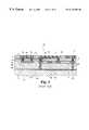
- FIG. 1illustrates further limitations of existing approaches.
- Integrated circuit 50 of FIG. 1includes substrate 52 with component connection sites 56 a, 56 b therealong.
- Oxide layer 60covers substrate 52 and defines via holes for metal via plugs 62 a, 62 b to electrically contact sites 56 a, 56 b, respectively.
- Layer 64is formed on top of layer 60 to provide a pattern of metal traces 66 insulated from each other by a dielectric—typically a silica (silicon dioxide) based material. Two of traces 66 are shown in electrical contact with plugs 62 a, 62 b to provide selected electrical contact with sites 56 a, 56 b, respectively.
- a dielectrictypically a silica (silicon dioxide) based material.
- Layer 70is formed on layer 64 and includes a pattern of metallic via plugs 72 insulated from each other by a dielectric—also usually a silica-based material.
- Layer 74is formed on layer 70 and includes a pattern of metal traces 76 insulated from each other in a similar manner to layer 64 .
- Plugs 72 of layer 70interconnect selected traces 66 and 76 of layers 64 and 74 , respectively, to provide a predetermined wiring pattern for circuit 50 .
- traces 66include a crossunder connection specifically designated by reference numeral 66 a to provide electrical coupling between two traces 76 of layer 74 that are separated by another trace specifically designated by reference numeral 76 b.
- traces 76include a crossover connection designated by reference numeral 76 a to provide electrical coupling between two traces 66 of layer 64 .
- crossover 76 ais routed around the trace specifically designated by reference numeral 66 b by elevation to the next metallization level of layer 74 .
- the crossover and crossunder connectionshave a longitudinal orientation that is generally perpendicular to the longitudinal orientation of other traces contained in the same layer. This orientation tends to limit the number of traces that may be included in a given layer.
- a similar limitation to the “packing density” of integrated circuit interconnectsarises from the occupation of layer “real estate” by dedicated, long-distance power supply bus traces in the same layer as long-distance signal carrying traces.
- power supply tracesare about 10 to 50 times wider than other types of signal routings.
- the more costly dielectric materials often utilized to preserve the integrity of long-distance, time-varying signal conductorsare usually not needed for power supply conductors.
- Traces designated by reference numerals 66 b, 76 b in layers 64 , 74are representative of power supply bus connections of existing integrated circuit arrangements.
- the present inventionsatisfies this need, generally improves integrated circuit layout flexibility, and provides other significant benefits and advantages.
- the present inventionrelates to techniques for interconnecting integrated circuit components.
- Various aspects of the inventionare novel, nonobvious, and provide various advantages. While the actual nature of the invention covered herein can only be determined with reference to the claims appended hereto, certain forms that are characteristic of the preferred embodiments disclosed herein are described briefly as follows.
- One form of the present inventionincludes a multilevel interconnection technique having crossover, crossunder, or local interconnects in a different connection layer than routing interconnects. These different connection layers are preferably separated by an insulative hard mask that functions as an etch stop layer relative to a dielectric included in the connection layers.
- a “routing interconnect”refers to an electrical connection that traverses several integrated circuit components; and a “local interconnect” refers to an electrical connection of two or more routing interconnects, two or more connection regions of the same integrated circuit component, or two or more connection regions of adjacent integrated circuit components.
- routing interconnectstypically provide longer range, lower resistance electrical coupling of components that are remotely located from each other.
- the connection layer dielectricbe comprised of a silica-based material and that the insulative hard mask be comprised of a silicon nitride or silicon oxynitride based material.
- Another formincludes an integrated circuit device with a number of electronic components along a semiconductor substrate and a first connection layer comprised of a first dielectric and a first number of conductors in selective electrical contact with the components.
- a first insulative layeris positioned on the first connection layer with a first pattern of openings therethrough.
- a second connection layercomprised of a second dielectric and a second number of conductors, a second insulative layer on the second connection layer with a second pattern of openings therethrough, and a third connection layer on the second insulative layer.
- the third connection layeris comprised of a third dielectric and a third number of conductors.
- the third dielectricis etch selective to the second insulative layer.
- the second and third conductorsare in contact with the second insulative layer and at least one of the second conductors crosses at least one of the third conductors, being electrically isolated therefrom by the second insulative layer.
- the second conductorsmay be utilized to form a number of overpass or crossover connections between the first conductors and a number of underpass or crossunder connections between the third conductors.
- the second conductorsmay include one or more power bus distribution conductors to free the first and third layers from providing the significant amount of space usually needed to accommodate power supply conductors. As a result, the first and third layers may have a comensurately higher routing interconnect density.
- a further formincludes provision for compatibility with Damascene integrated circuit architecture.
- This formincludes providing an integrated circuit device with a number of electronic components on a substrate and planarizing a first dielectric layer formed over the components.
- a first insulative hard maskis formed on the first layer and a second dielectric layer on the first hard mask.
- a first pattern of openingsis defined through the first hard mask.
- the first and second layersare etched selective to the first hard mask to form a first number of recesses in the second layer with a portion of the recesses corresponding to the first pattern of openings extending through the first layer.
- the first recessesare at least partially filled to define a first number of conductors in selective contact with the components through the first pattern of openings.
- a second insulative hard maskis deposited on the second layer and a third dielectric layer is deposited on the second hard mask.
- the third layeris etched selective to the second hard mask to define a second number of recesses therein that are at least partially filled to define a second number of conductors selectively connecting the first conductors through a second pattern of openings defined in the second hard mask.
- a third insulative hard maskis deposited on the third layer and a fourth dielectric layer is deposited on the third hard mask.
- the fourth layeris etched selective to the third hard mask to form a third number of recesses that are at least partially filled to define a third number of conductors selectively connected by the second conductors through a third pattern of openings defined in the third hard mask. At least a portion of the first and third conductors are routing interconnects.
- Yet another formincludes providing a number of electronic components on a substrate and selectively removing a first dielectric layer deposited over the components to define a first number of recesses each exposing at least two electrical contact surfaces of the components.
- the first recessesare each generally filled to provide a corresponding number of local interconnects.
- a first insulative hard maskis formed on the first layer and local interconnects, and a second dielectric layer including a first number of conductors is formed over the first hard mask.
- the first conductorsare selectively electrically coupled to the components through a first pattern of openings in the first hard mask.
- a second hard mask with a second pattern of openingsis formed over the second layer.
- a third dielectric layer in contact with the second hard maskis formed and the third layer is etched selective to the second hard mask to form a second number of recesses.
- the second recessesare at least partially filled to define a second number of conductors in the third layer that selectively connect the first conductors through a second pattern of openings defined by the second hard mask.
- the first conductors and the second conductorsare in contact with the second hard mask.
- connection layersseparated by hard masks, where the dielectric of the connection layers and the hard masks may be etched selective to each other.
- FIG. 1is a partial, sectional view of an existing integrated circuit.
- FIGS. 2 - 12are partial, sectional side views of an integrated circuit device as it progresses through selected processing stages 100 a - 100 k in accordance with one embodiment of the present invention.
- FIGS. 13 - 25are partial, sectional side views of an integrated circuit device as it progresses through selected processing stages 200 a - 200 m in accordance with another embodiment of the present invention.
- FIG. 26is a partial, cut-away, top view of the integrated circuit device shown in FIG. 12 .
- FIG. 27is a partial, top view of the integrated circuit device shown in FIG. 25 .
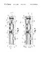
- FIGS. 2 - 12depict partial, cross-sectional side views of selected stages 100 a - 100 k in the manufacturing process 100 of integrated circuit device 101 .
- device 101is depicted after various front-end processing has been performed.
- Device 101includes semiconductor substrate 102 .
- Substrate 102is preferably of a generally planar form that extends perpendicular to the view plane of FIG. 2 .
- substrate 102be of the single-crystal silicon variety; however, other substrate compositions may be utilized as would occur to those skilled in the art.
- Device 101also includes electrical isolation structure 104 .
- Structure 104comprises a dielectric-filled recess in substrate 102 formed in accordance with shallow trench isolation techniques. In other embodiments, such isolation structures may not be utilized or a different isolation structure variety may be employed.
- Structure 104bounds component region 105 having several integrated circuit components 110 .
- Component region 105includes doped regions 106 a, 106 b, 106 c. Typically, regions 106 a - 106 c are of one conductivity type and positioned in a well of substrate 102 doped with the opposite conductivity type to form desired p-n junctions for components 110 .
- Silicide substrate regions 108 a, 108 b, 108 care correspondingly positioned over regions 106 a, 106 b, 106 c and are in electrical contact therewith to facilitate electrical contacts with components 110 as needed.
- Components 110include a number of Insulated Gate Field Effect Transistors (IGFETs) 112 a, 112 b, 112 c. IGFET 112 c is only partially shown. IGFETs 112 a, 112 b, 112 c each include a corresponding insulated gate 114 a, 114 b, 114 c upwardly extending away from substrate 102 along the view plane of FIG. 2 . Each gate 114 a, 114 b, 114 c includes dielectric pad 116 , a polycrystalline silicon portion 117 on pad 116 , and a silicide portion 118 on portion 117 .
- IGFETsInsulated Gate Field Effect Transistors
- Pad 116 , portion 117 , and portion 118are collectively bounded by a pair of dielectric spacer walls 119 .
- Gates 114 a - 114 ccooperate with doped regions 106 a - 106 c to define channel areas beneath pads 116 and corresponding source and drain areas for each transistor 112 a - 112 c.
- regions 106 b and 106 care disposed as common source or drain areas with respect to transistors 112 a - 112 c.
- Components 110 of device 101may include additional transistors, resistors, diodes, capacitors, fuses, or other active or passive integrated circuit component types as would occur to those skilled in the art.
- front-end processing of device 101 to reach stage 100 abegins with the formation of isolation structures, such as structure 104 , using conventional techniques.
- transistorsare formed beginning with the establishment of corresponding n- and p-wells in substrate 102 using standard techniques.
- a suitable gate dielectric layeris formed on substrate 102 from which pads 116 will be provided.
- the gate dielectricis formed from a silicon dioxide layer having a thickness of about 54 angstroms.
- an amorphous silicon layeris deposited thereon. The amorphous silicon layer and gate dielectric layer are patterned to form strips corresponding to gates 114 a - 114 b using standard photolithographic techniques.
- Gate spacerssuch as spacer walls 119 , are formed as part of the front-end processing, preferably in conjunction with a Lightly Doped Drain (LDD) formation procedure.
- LDDLightly Doped Drain
- source/drain formationincludes depositing an implant screen oxide layer on device 101 , and implanting substrate 102 with n+ or p+ dopant to form regions such as those designated by reference numerals 106 a - 106 c.
- n+ implantationmay be accomplished by implanting ionized arsenic atoms (As) at about 60 Kev 2 ⁇ 10 15 cm ⁇ 2 ; and p+ implantation may be accomplished by implanting ionized boron difluouride (BF 2 ) at about 50 keV 3 ⁇ 10 15 cm ⁇ 2 .
- implantationis preferably followed by a Rapid Thermal Anneal (RTA) at about 1000° C. for about 30 seconds to activate the implanted dopants.
- RTARapid Thermal Anneal
- Front-end processingalso typically changes the crystal lattice of the amorphous silicon into polycrystalline silicon (“polysilicon”).
- silicide formationtakes place.
- the formation of silicide substrate regions 108 a - 108 c and silicide portions 118may be accomplished by blanketing device 101 with a suitable metal such as titanium (Ti), cobalt (Co), or nickel (Ni); although other materials suitable for silicidation are also contemplated.
- a suitable metalsuch as titanium (Ti), cobalt (Co), or nickel (Ni); although other materials suitable for silicidation are also contemplated.
- RTArapid thermal anneal
- silicon from substrate 102would preferably be consumed.
- gates 114 a - 114 csilicon from polycrystalline silicon portions 117 would be consumed by this process.
- the unconsumed part of the metal layeris typically removed by an etching process. Following removal of the excess metal, additional rapid thermal anneals may be performed.
- a second Rapid Thermal AnnealRTA
- a first RTA at about 720 degrees for about 30 seconds, followed by a wet etch to remove excess Ti, and a second RTA at about 850 degrees Celsius for about 30 secondsis preferred.
- silicide portions 118may be formed independently of the silicide substrate regions 108 a - 108 c.
- different front-end processing of device 101may be utilized as would occur to those skilled in the art.
- a dielectric barrier layer 120is deposited that blankets device 101 .
- barrier layer 120is formed from silicon nitride or silicon dioxide; however, other compositions may be utilized as would occur to one skilled in the art. Indeed, in one alternative embodiment, a barrier layer 120 is not utilized at all.
- Dielectric filler layer 122is deposited on layer 120 , having a thickness greater than the collective thicknesses of pad 116 , polycrystalline silicon portion 117 , and silicide portion 118 to generally fill space between gates 114 a - 114 c and cover substrate 102 .
- layer 122is formed by coating device 101 with a silicon dioxide based dielectric and then planarizing device 101 with a compatible Chemical-Mechanical Polishing (CMP) technique to define generally planar surface 123 .
- CMPChemical-Mechanical Polishing
- An insulative layer 124is formed on surface 123 .
- Photoresist pattern 126is then formed on layer 124 using standard photolithographic techniques. Pattern 126 is depicted with openings 126 a, 126 b which expose corresponding regions of layer 124 .
- Layer 124is preferably formed from a material that may be etched selective to layer 122 in accordance with pattern 126 . Pattern 126 is utilized to selectively etch layer 124 and transform it into an insulative etch stop hard mask 130 with a pattern of openings 131 , including openings 131 a, 131 b corresponding to openings 126 a, 126 b as shown in stage 100 b of FIG. 3 . After forming hard mask 130 from layer 124 , pattern 126 is stripped in a standard fashion to provide device 101 as shown in stage 100 b.
- layer 124is provided by a coating of silicon nitride (SiN) or silicon oxynitride (SiON) with a thickness of less than about 1,000 angstroms.
- pattern 126has a relatively thin thickness of about 3,000 angstroms to provide an optimum amount of focus latitude for photolithographic equipment used in the patterning process. Such focus latitude facilitates formation of a high resolution pattern in pattern 126 and correspondingly in pattern 131 .
- the antireflective properties of silicon nitride or silicon oxynitride for layer 124facilitates the reduction of reflections which tend to distort patterns produced by photolithographic processing.
- Progression from stage 100 b of FIG. 3 to stage 100 c of FIG. 4is accomplished by depositing dielectric layer 132 on hard mask 130 that generally fills openings 131 a, 131 b.
- dielectric layer 132may be etched selective to hard mask 130 .
- hard mask 130behaves as an etch stop relative to layer 132 .
- dielectric 132be formed by depositing a flowable, low dielectric constant Spin-On-Glass (SOG) to maintain a generally planar structure while still filling openings 131 a, 131 b of pattern 131 .
- SOGSpin-On-Glass
- a low dielectric constant material or “low-k dielectric”is typically desired between long-distance routing interconnects that carry time varying signals to reduce capacitive losses.
- such materialsare usually more costly than dielectrics with a higher dielectric constant (“high-k dielectrics”) and are often more difficult to process effectively.
- high-k dielectricsdielectric constant
- preferred SOGs for dielectric 132are nonstoichiometric forms of a silica-based glass.
- dielectric layer 132be formed by spinning on Hitachi Silica Glass (HSG) supplied by Kabushiki Kaisha Hitachi Seisakusho (Japanese Corporation); d/b/a Hitachi, Ltd., with a business address of 6 Kanda-Surugadai, 4 Chome, Choyoda-Ku, Tokyo, Japan.
- HSGHitachi Silica Glass
- a material with a relatively higher dielectric constantsuch as tetraethylorthosilicate (TEOS) or phosphosilicate Glass (PSG) is preferred.
- TEOStetraethylorthosilicate
- PSGphosphosilicate Glass
- Dielectric layer 132is masked with photoresist pattern 133 in stage 100 c using common techniques.
- Pattern 133defines openings 133 a - 133 d to expose corresponding regions of layer 132 .
- openings 133 a and 133 dcorrespond to openings 131 a and 131 b of pattern 131 of hard mask 130 .
- Photoresist Pattern 133is utilized to selectively remove layer 132 where exposed through openings 133 a - 133 d selective to hard mask 130 to correspondingly form recesses 135 as shown in stage 100 d of FIG. 5 . Further removal takes place through openings 131 a, 131 b into layer 122 .
- selective removal of layers 132 and layer 122 through pattern of openings 131is performed using a common etching procedure that is selective to hard mask 130 .
- Stage 100 dfurther shows device 101 after photoresist pattern 133 has been stripped.
- the formation of recesses 135transforms layers 122 , 132 , into patterned dielectrics 142 , 152 , respectively.
- Recesses 135include channels 136 a - 136 d defined by dielectric 152 and via holes 137 a and 137 b defined by dielectric 142 .
- Via holes 137 a, 137 bintersect channels 136 a and 136 d through openings 131 a, 131 b, respectively.
- Hard mask 130defines the lower limit for channels 136 a - 136 d where present.
- channels 136 a and 136 dhave a greater width than the corresponding via holes 137 a and 137 b to improve tolerance to any misalignment of pattern 133 relative to hard mask 130 .
- FIG. 5also shows that portions of barrier layer 120 corresponding to via holes 137 a, 137 b have been removed to expose silicide component connection regions 138 a and 138 b, respectively.
- barrier layer 120is formed of a nitride compound, removal of it may be performed separately, selective to layers 132 and 122 . This approach may also remove some or all of hard mask 130 exposed in channels 136 a - 136 d (not shown), but removal at this stage does not impact integrity of device 101 as will become apparent in connection with the description of later stages.
- barrier layer 120may be removed selective to hard mask 130 or may be mutually etched with layers 122 or 132 .
- barrier layer 120may be absent.
- Stage 100 e of FIG. 6results from the subsequent deposition of a conductive material in recesses 135 to form a corresponding number of conductors 139 .
- Conductors 139include plug conductors 144 a, 144 b in via holes 137 a, 137 b defined by patterned dielectric 142 . Collectively, conductors 144 a, 144 b and dielectric 142 form connection layer 140 . Conductors 144 a, 144 b electrically contact component connection regions 138 a, 138 b. Also, conductors 139 include routing interconnect conductors 153 a - 153 d in channels 136 a - 136 d defined by patterned dielectric 152 .
- conductors 153 a - 153 d and dielectric 154form connection layer 150 .
- Conductors 153 a - 153 d and channels 136 a - 136 dare elongate, running for relatively long distances in a direction perpendicular to the view plane of FIG. 6 to provide routing interconnects between various components of device 101 (not shown). Such long-distance runs may also be used to provide selected signals to other circuit components (such as buffers, filters, memory cells, and the like) or to external bonding pads (not shown).
- conductors 153 a and 153 dare integrally formed with conductors 144 a and 144 b of connection layer 140 by passage of the conductive material through openings 131 a and 131 b of hard mask 130 , respectively.
- the conductive material deposited in recesses 135is a metal suitable for electrical interconnections in an integrated circuit device.
- a metal suitable for electrical interconnections in an integrated circuit deviceFor example, aluminum (Al), cobalt (Co), copper (Cu), gold (Au), nickel (Ni), platinum (Pt), silver (Ag), titanium (Ti), or tungsten (W) may be appropriate for the formation of conductive members 139 using suitable deposition techniques as are known to those skilled in the art.
- a Chemical Vapor Deposition (CVD), a Physical Vapor Deposition (PVD), a force-fill technique, or any other technique known to those skilled in the artmay be used that is suitable for the selected conductive material.
- conductive materialmay include one or more desired barrier or adhesion layers to facilitate a suitable interconnection arrangement as are known to those skilled in the art.
- conductors 144 a, 144 bare formed from one type of conductive material and conductors 153 a - 153 d are provided from another type of conductive material.
- device 101is planarized by a compatible process such as Chemical-Mechanical-Polishing (CMP) or blanket etching. It is also preferred that this process remove any excess conductive material residing outside of recesses 135 .
- CMPChemical-Mechanical-Polishing
- Stage 100 f of FIG. 7depicts device 101 after insulative layer 156 is formed on connection layer 150 .
- layer 156may be etched in the same manner as hard mask 130 .
- hard mask 130 and layer 156are each formed from the same nitride or silicon oxynitride composition to serve as etch stops for silica-based dielectrics positioned therebetween, and further to provide desirable antireflective properties.
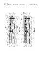
- Hard mask 160includes a pattern of openings 161 , a few of which are specifically designated as openings 161 a, 161 b, 161 c. Openings 161 a, 161 b, 161 c expose surfaces 154 a, 154 c, 154 d of conductors 153 a, 153 c, 153 d, respectively. As shown in stage 100 h of FIG. 9, dielectric layer 162 is deposited on hard mask 160 that generally fills and planarizes openings 161 a - 161 c.
- Layer 162is preferably comprised of an oxide of silicon that is etch selective to hard mask 160 and need not be of the low-k variety. More preferably, dielectric layer 162 is formed from a tetraethylorthosilicate (TEOS) or a Phosphosilicate Glass (PSG). Photoresist pattern 164 is formed on dielectric layer 162 using standard photolithographic techniques. Pattern 164 includes openings 164 a - 164 c. In progressing from stage 100 h of FIG. 9 to stage 100 i of FIG. 10, dielectric layer 162 is selectively removed in accordance with pattern 164 to form patterned dielectric 172 therefrom. Preferably, removal is performed by conventional dry etching. Pattern 164 is then stripped off device 101 as shown in FIG. 10 .
- TEOStetraethylorthosilicate
- PSGPhosphosilicate Glass
- Dielectric 172accordingly defines recesses 172 a - 172 e. Recesses 172 a - 172 e bottom-out on hard mask 160 where present as a result of its etch-stop characteristics. A conductive material is deposited in recesses 172 a - 172 e to form conductors 173 a - 173 e, where conductor 173 a is partially shown. Hard mask 160 insulates conductors 173 a - 173 c from unintentional electrical contact with conductors 153 a - 153 d of layer 150 . Collectively, dielectric 172 and conductors 173 a - 173 e define connection layer 170 .
- connection layer 170includes via plugs, such as conductor 173 e, and elongate conductors, such as conductors 173 b and 173 c, that are oriented with their longitude along an axis that is generally parallel to the view plane of FIG. 10 and perpendicular to the longitudinal axis of conductors 153 a - 153 d in connection layer 150 below.
- conductors of connection layer 170may be used to provide a relatively short-run connections between conductors 153 a - 153 d such as conductor 173 c, which is further designated crossover or overpass connection 174 .
- Connection 174interconnects conductors 153 a and 153 c of connection layer 150 through openings 161 a and 161 b.
- conductor 173 ccrosses conductor 153 b of connection layer 150 with electrical isolation being maintained by hard mask 160 positioned therebetween.
- the conductive material used to form conductors 173 a - 173 eis preferably tungsten (W) that is deposited using CVD; or copper (Cu) or aluminum (Al) (or suitable alloys thereof) using a force fill technique.
- device 101is preferably planarized by a compatible CMP process. However, in other embodiments a different conductive material and planarization technique may be utilized as would occur to those skilled in the art.
- FIG. 11depicts stage 100 j which includes the addition of hard mask 180 and dielectric layer 182 to device 101 after stage 100 i.
- hard mask 180is composed of a silicon nitride (SiN) or silicon oxynitride (SiON) and is formed using techniques like those used in the formation of hard masks 130 and 160 .
- Dielectric layer 182is formulated to be etch selective to hard mask 180 and is preferably formed from two consecutive spun-on coatings 182 a, 182 b of a low-k or SOG dielectric, such as HSG. Coating 182 a fills openings 181 a - 181 c included in pattern of openings 181 of hard mask 180 . Two coatings of SOG facilitate planarization, low-k performance, and subsequent laser customization. In other embodiments, a different dielectric composition including fewer or more coatings may be utilized.
- stage 100 killustrates device 101 after dielectric layer 182 has been patterned to form connection layer 190 .
- Connection layer 190includes patterned dielectric 192 formed from layer 182 and routing interconnect conductors 193 a - 193 h.
- Dielectric 192is preferably formed using techniques comparable to those used to transform dielectric layers 122 , 132 , 162 to patterned dielectrics 142 , 152 , 172 , respectively.
- Dielectric 192defines recesses 192 a - 192 h that are filled with a conductive material to form routing interconnect conductors 193 a - 193 h.
- conductors 193 a - 193 hare formed from the same conductive material as conductors 153 a - 153 d of connection layer 150 using comparable techniques.
- conductors 193 a - 193 hmay be in contact with hard mask 180 which prevents unwanted electrical contact with conductors of layer 170 .
- conductors 193 a - 193 h of connection layer 190are longitudinally oriented in a direction generally perpendicular to the view plane of FIG. 12 and generally parallel to the longitudinal axis of conductors 153 a - 153 d of connection layer 150 .
- the elongate conductors of connection layer 170are oriented generally crosswise to conductors 193 a - 193 h and 153 a - 153 d.
- This arrangementfacilitates overpass or crossover connections, such as connection 174 ; and underpass or crossunder connections, such as conductor 173 b, which has been further designated underpass or crossunder connection 175 .
- Connection 175interconnects conductors 193 a and 193 c through openings 181 a and 181 b of hard mask 180 , respectively.
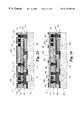
- FIG. 26further illustrates the orientation of conductors in the different layers by providing a partial, top view of device 101 at stage 100 k.
- selected features below layer 190are shown in phantom.
- routing interconnect conductors 193 a - 193 hare generally parallel to each other with a longitudinal axis L 1 .
- FIG. 26shows additional components 110 in regions 105 a and 105 b that are not shown in FIG. 12 .
- Regions 105 a, 105 bare separated from each other by isolation structure 104 a.
- structure 104 ais formed in the same manner as structure 104 .
- FIG. 26also illustrates the configuration of conductors 193 a - 193 h as routing interconnects that traverse several active silicon components 110 .
- conductors 193 a - 193may widely disperse signals over relatively long distances and provide interconnection of remotely located components.
- Interconnection to components 110 by conductors 193 a - 193 his provided through layers 140 , 150 , 170 and hard masks 130 , 160 , 180 as illustrated, for example, in FIG. 12 by via stack 176 that interconnects region 138 b to conductor 193 h.
- Conductors 153 a - 153 dare also configured as routing interconnects along longitudinal axis L 1 (not shown).
- Connection level 195is preferably comprised of contact-type connections to regions of components 110 , such as plug conductors 144 a, 144 b.
- Connection levels 196 and 198provide generally long-run routing interconnects that traverse several components of device 101 as further depicted in FIG. 26 .
- Connection level 197positioned between routing levels 196 and 198 provides crossover, crossunder, and via plug connections that serve levels 196 , 198 .
- Hard masks 130 , 160 , 180provide selective interconnection of levels 195 - 198 and may contact conductors at levels 196 - 198 while maintaining desired electrical isolation.
- hard masks and connection levels above components 110are generally planar in form to facilitate alignment and process control. These are but a few of the aspects of the present invention that facilitate a more flexible, higher density interconnection structure.
- the interconnection structure of device 101also facilitates the distribution of power supply conductors in a manner that facilitates a higher interconnection density.
- distribution linesmay be provided, for example, by conductors 173 a, 173 d in level 197 , instead of sharing the same level as routing interconnects.
- This arrangementmakes more routing interconnect space available in levels 196 and 198 .
- the pervasive nature of power supply conductor distributionstypically interferes with efficient high-density routings for long-distance signals in levels 196 , 198 .
- the relatively short connections and via plugs in the intervening level 197do not suffer as greatly by inclusion of an extensive distribution of power supply conductors.
- power supply distribution conductorstypically do not need the benefits provided by such materials; thus further supporting the location of the power supply conductors in level 197 .
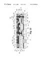
- FIGS. 13 - 25progressively illustrate selected stages 200 a - 200 m of interconnection process 200 .
- FIG. 13illustrates intermediate stage 200 a of integrated circuit device 201 .
- Device 201has substrate 102 and isolation structure 104 previously described in connection with process 100 and device 101 ; where like reference numerals refer to like features.
- device 201includes doped regions 106 a - 106 c and silicide substrate regions 108 a - 108 c as are further described in connection with device 101 .
- An additional silicide substrate region 208is also identified in FIG. 13 .
- Device 201also includes component region 205 with integrated circuit components 210 .
- integrated circuit components 210may include transistors, resistors, capacitors, and other active or passive component types known to those skilled in the art.
- FIG. 13specifically designates three transistor gate structures 214 a - 214 c, where 214 c is only partially shown.
- Substrate 102 and regions 106 a - 106 care arranged as discussed in connection with device 101 to provide IGFET transistors corresponding to gate structures 214 a - 214 c, that are generally designated by reference numeral 212 .
- Gates 214 a - 214 chave the same features described in connection with gates 114 a - 114 c of device 101 , including a dielectric gate pad, polysilicon portion, and silicide portion stack that is bounded by a corresponding pair of dielectric spacer walls. Different reference numerals 214 a - 214 c are used to distinguish these structures as they are processed differently in later stages corresponding to FIGS. 14 - 25 . Front-end processing of the device 101 to provide substrate 102 , isolation structure 104 , and components 210 as shown in FIG. 13 may be performed in the manner described for device 101 .
- barrier layer 220that is preferably formed from silicon nitride.
- a filler dielectric layer 222is deposited on barrier layer 220 and has a thickness sufficient to fill space between gates 214 a - 214 c and exceeds their height above substrate 102 .
- dielectric layer 222is comprised of a silica-based material.
- Stage 200 b of FIG. 14shows device 201 after planarization.
- planarizationis performed by a conventional CMP procedure, removing a portion of layer 220 , layer 222 , and gates 214 a - 214 c resulting in generally planar surface 223 .
- the planarization processexposes the remaining polysilicon members 217 a, 217 b of corresponding gates 214 a, 214 b and results in shortened spacers 219 .
- silicide substrate regions 108 a - 108 c and 208remain covered by portions of barrier layer 220 and dielectric layer 222 .
- etch-back chemistryincludes chlorine gas and Hydrogen Bromide (HBr) at a temperature of about 60° C.; however, other etch chemistries or removal techniques may be employed as would occur to those skilled in the art.
- photoresist pattern 226is provided on device 201 as illustrated in stage 200 d of FIG. 16 using conventional lithography techniques.
- Pattern 226defines openings 226 a - 226 c for subsequent processing of device 201 .
- pattern 226fills recesses 224 a, 224 b of corresponding gates 214 a, 214 b.
- recesses 235 a - 235 care formed in correspondence with openings 226 a - 226 c of pattern 226 .
- Recesses 235 a - 235 care preferably formed by etching portions of dielectric layer 222 exposed through openings 226 a - 226 c selective to barrier layer 220 and then layer 220 is etched where exposed in recesses 235 a - 235 c selective to layer 222 using conventional techniques. If spacer 219 in recess 235 b is formed from a dielectric that is mutually etched with layer 222 , it may also be at least partially removed when layer 222 is removed to the extent it is exposed (not shown).
- layer 222be etched selective to the dielectric comprising spacer 219 and that spacer 219 be mutually etched with layer 220 selective to layer 222 .
- stage 200 f of FIG. 18a portion, but not all, of spacer 119 in recess 235 b has been removed to become generally level with polysilicon member 117 b of gate 214 b.
- silicide substrate regions 108 a - 108 c and 208become selectively exposed to facilitate local electrical interconnection.
- Recesses 235 b and 224 bintersect one another in stage 200 f. The formation of recesses 235 a - 235 c transform layer 222 into patterned dielectric 232 .
- a conductive materialis deposited to generally fill recesses 224 a, 224 b, 235 a, 235 b, 235 c.
- the conductive materialis a metal that may be deposited by a conventional process followed by planarization of device 101 to remove metal lying outside of the corresponding recesses.
- tungstenis deposited through a chemical vapor deposition of tungsten hexafluoride (WF 6 ) followed by a compatible CMP to remove excess metal; however, other conductive materials and deposition processes may be utilized as would occur to those skilled in the art.
- the resulting conductors 237include local interconnect 239 a bridging isolation structure 104 and connecting silicide substrate regions 208 and 108 a.
- recess 224 a formed in gate 214 ais filled to define a conductive cap 239 b.
- Local interconnect 239 cbridges silicide substrate region 108 b and polysilicon member 217 b of gate 214 b.
- Silicide substrate region 108 cis electrically connected to via plug 239 d.
- Collectively, patterned dielectric 232 and conductors 237constitute connection layer 240 .
- Hard mask 260includes openings 260 a - 260 d. Hard mask 260 may be formed using the same materials and processes as hard masks 130 , 160 , and 180 of device 101 .
- Patterned dielectric 262is formed over hard mask 260 from a material that may be etched selective to hard mask 260 .
- Dielectric 262defines a number of via holes 262 a - 262 d aligned with openings 260 a - 260 d of hard mask 260 .
- a conductive materialis deposited in via holes 262 a - 262 d to define corresponding conductors of a plug or cap type designated by reference numerals 263 a - 263 d.
- hard mask 260is comprised of silicon nitride or silicon oxynitride to provide antireflective characteristics as well as an etch-stop capability relative to dielectric 262 .
- dielectric 262be comprised of a silica-based compound such as TEOS or PSG.
- conductors 237 for connection layer 240it is preferred that conductors 263 a - 263 d be formed by a chemical vapor deposition of tungsten in openings 262 a - 262 d, respectively, followed by an appropriate CMP procedure to generally maintain planarity and remove any excess metal.
- device 201has been further processed to include patterned dielectric 272 and routing interconnect conductors 273 a - 273 g.
- Dielectric 272 and conductors 273 a - 273 gmay be formed using conventional processes.
- conductor layer stack 275is illustrated.
- Stack 275includes upper diffusion barrier/adhesion layer 276 a and lower diffusion barrier/adhesion layer 276 b. Between layers 276 a and 276 b is primary conductive layer 277 . This arrangement of stack 275 is particularly suited for long-run routing interconnects where a highly conductive material such as copper or aluminum is desired that may otherwise diffuse into the surrounding material or not properly adhere to it.
- copper or aluminumpreferably constitute the primary conductive layer 277 with compatible compositions for barrier/adhesion layers 276 a, 276 b.
- a titanium nitride formulation of layers 276 a, 276 bis preferred.
- connection layer 270Collectively, dielectrics 262 , 272 and conductors 263 a - 263 b, 273 a - 273 g constitute connection layer 270 as illustrated in FIG. 21 .
- Conductors 273 a - 273 gare elongate, having a longitudinal axis that is generally perpendicular to the view plane of FIG. 21 .
- Conductors 237 of connection layer 240may further be utilized to electrically couple selected conductors of connection layer 270 .
- local interconnect 239 aelectrically couples conductors 273 a and 273 c via conductors 263 a and 263 b, respectively, to additionally provide an underpass or crossunder type of connection.
- Conductors 273 a - 273 gare formed using conventional photolithographic techniques.
- dielectric 272is formed from a spun-on coating of a low-k SOG, such as HSG.
- dielectric 262 and corresponding conductors 263 a - 263 dare not utilized. Instead, conductors 273 a - 273 g and dielectric 272 are formed directly on hard mask 260 .
- connection layer 270comprises a single layer of patterned dielectric with corresponding conductors spaced therethrough.
- interconnection formationwould be adapted for direct contact with routing interconnects through openings 260 a - 260 d in hard mask 260 .
- Stage 200 jis shown in FIG. 22 that indicates further processing of device 201 by adding insulative layer 275 .
- insulative layer 275is formed from the same material as hard mask 260 .
- a photoresist pattern 277is formed using conventional photolithographic techniques which defines a number of openings 277 a - 277 e over selected conductors 273 a, 273 b, 273 d, 273 e, 273 g; respectively.
- Selective removal of layer 275is performed in accordance with pattern 277 to define openings 280 a - 280 e, and correspondingly form hard mask 280 as shown in stage 200 l of FIG. 24 .
- Pattern 277is stripped after formation of openings 280 a - 280 e.
- Stage 200 lalso reflects further processing of device 201 by depositing another relatively thick dielectric layer 282 that is preferably of a TEOS or PSG composition. Once deposited, layer 282 is planarized, preferably by a compatible CMP procedure. Layer 282 is preferably formed from a material that is etch selective to hard mask 280 . Photoresist pattern 283 is then defined on top of layer 282 with openings 283 a - 283 d, using conventional photolithographic techniques.
- FIG. 25depicts device 201 at processing stage 200 m.
- layer 282has been selectively removed, preferably by conventional etching, to form patterned dielectric 292 therefrom.
- Dielectric 292defines recesses 292 a - 292 d corresponding to openings 283 a - 283 d of pattern 283 .
- Recesses 292 a - 292 dare filled with a conductive material to provide additional conductors 293 a - 293 d.
- conductor 293 ais a via plug and conductors 293 b, 293 d are crossover or overpass connections.
- conductors 293 a - 293 dbe formed from a metal, such as tungsten (W), using a conventional fill technique followed by removal of any excess metal outside recesses 292 a - 292 d.
- dielectric 292 and conductors 293 a - 293 ddefine connection layer 290 .
- device 201includes interconnection levels 295 , 296 , 297 .
- Level 295preferably provides short-run connections such as via plugs, local interconnects, and underpass or crossunder connections for higher levels.
- level 296provides routing interconnects over relatively long distances through device 201 .
- Level 297is preferred for additional short-run connections such as the via plug, crossover, or overpass variety, and may also be utilized for conductors carrying relatively time-invariant signals such as power supply busses.
- FIG. 27a partial, cut-away top view of device 201 at stage 200 m is presented. Selected features of layer 290 and 270 are shown in solid lines and selected features below layer 270 are shown in phantom. FIG.
- FIG. 27further depicts components 210 in regions 205 a and 205 b not shown in FIG. 25 . Regions 205 a and 205 b are separated by isolation structure 104 a as described in connection with FIG. 26 .
- the routing interconnect arrangement of each conductor 273 a - 273 gis also further illustrated in FIG. 27 . Conductors 273 a - 273 b are generally parallel to each other extending along their longitudinal axis L 2 over components 210 .
- the segregation of routing interconnects for high speed signals from other types of connectionsprovides a more efficient allocation of low-k dielectrics and facilitates higher interconnect density by increasing routing uniformity at little increase in terms of cost and processing complexity.
- the separation of connection layer dielectrics with insulative hard masks that may be etched selective to each otherenhances interconnection process control—especially as the critical dimensions of integrated circuit components continue to shrink below 0.25 micron. If the preferred interconnection arrangement leads to contact of a SOG dielectric of a connection layer with a silicon nitride or silicon oxynitride hard mask, wettability may be improved by a surface treatment with an H 2 O-plasma or dry O 2 ash.
- process 100is applied to further layout flexibility beyond conventional Damascene techniques and thereby enable interconnection of devices having critical dimensions of less than about 0.20 micron.
- Process 200is preferably applied devices having a critical dimension in the range of about 0.25 to about 0.35 micron.
- processes 100 , 200may be applied to devices having any critical dimension.
- stages 100 a - 100 k and 200 a - 200 m of processes 100 and 200 , respectivelymay be intermixed, rearranged, substituted, deleted, duplicated, combined, or added as would occur to those skilled in the art.
- fewer or more connection layersmay be utilized in either process 100 , 200 .
- the connection layers of processes 100 and 200may be intermixed in alternative embodiments to optimize the interconnection approach best-suited to a particular integrated circuit arrangement.
- devices 101 , 102include only a few representative integrated circuit components 110 , 210 , respectively.
- the present inventionwould be applied to devices having a greater quantity of integrated circuit components than depicted; however, illustrating such quantities would needlessly complicate the figures.
- different active or passive integrated circuit component typesas would occur to those skilled in the art may additionally or alternatively be included, but have not been specifically described to enhance clarity.
Landscapes
- Physics & Mathematics (AREA)
- Engineering & Computer Science (AREA)
- Condensed Matter Physics & Semiconductors (AREA)
- General Physics & Mathematics (AREA)
- Computer Hardware Design (AREA)
- Microelectronics & Electronic Packaging (AREA)
- Power Engineering (AREA)
- Geometry (AREA)
- Manufacturing & Machinery (AREA)
- Internal Circuitry In Semiconductor Integrated Circuit Devices (AREA)
Abstract
Description
Claims (24)
Priority Applications (1)
| Application Number | Priority Date | Filing Date | Title |
|---|---|---|---|
| US09/154,050US6174803B1 (en) | 1998-09-16 | 1998-09-16 | Integrated circuit device interconnection techniques |
Applications Claiming Priority (1)
| Application Number | Priority Date | Filing Date | Title |
|---|---|---|---|
| US09/154,050US6174803B1 (en) | 1998-09-16 | 1998-09-16 | Integrated circuit device interconnection techniques |
Publications (1)
| Publication Number | Publication Date |
|---|---|
| US6174803B1true US6174803B1 (en) | 2001-01-16 |
Family
ID=22549786
Family Applications (1)
| Application Number | Title | Priority Date | Filing Date |
|---|---|---|---|
| US09/154,050Expired - LifetimeUS6174803B1 (en) | 1998-09-16 | 1998-09-16 | Integrated circuit device interconnection techniques |
Country Status (1)
| Country | Link |
|---|---|
| US (1) | US6174803B1 (en) |
Cited By (51)
| Publication number | Priority date | Publication date | Assignee | Title |
|---|---|---|---|---|
| US20010008794A1 (en)* | 2000-01-13 | 2001-07-19 | Masatoshi Akagawa | Semiconductor device and manufacturing method therefor |
| US6294834B1 (en)* | 2000-01-21 | 2001-09-25 | United Microelectronics Corp. | Structure of combined passive elements and logic circuit on a silicon on insulator wafer |
| US6329695B1 (en)* | 1999-01-06 | 2001-12-11 | Advanced Micro Devices, Inc. | Merged sidewall spacer formed between series-connected MOSFETs for improved integrated circuit operation |
| US20020008324A1 (en)* | 2000-07-21 | 2002-01-24 | Mitsubishi Denki Kabushiki Kaisha | Semiconductor device and method of manufacturing same |
| US6380067B1 (en)* | 2000-05-31 | 2002-04-30 | Advanced Micro Devices, Inc. | Method for creating partially UV transparent anti-reflective coating for semiconductors |
| US6426558B1 (en)* | 2001-05-14 | 2002-07-30 | International Business Machines Corporation | Metallurgy for semiconductor devices |
| US6437640B1 (en)* | 2000-09-12 | 2002-08-20 | The Aerospace Corporation | Addressable diode isolated thin film array |
| US6459155B1 (en)* | 2000-12-05 | 2002-10-01 | Advanced Micro Devices, Inc. | Damascene processing employing low Si-SiON etch stop layer/arc |
| US6479873B1 (en)* | 1999-06-10 | 2002-11-12 | Mitsubishi Denki Kabushiki Kaisha | Semiconductor device with self-aligned contact structure |
| US20020177287A1 (en)* | 2000-01-21 | 2002-11-28 | Lucent Technologies Inc. | Capacitor for integration with copper damascene processes and a method of manufacture therefore |
| US20030001270A1 (en)* | 1999-07-12 | 2003-01-02 | Mitsubishi Denki Kabushiki Kaisha | Semiconductor device having an improved multi-layer interconnection structure and manufacturing method thereof |
| US6503830B2 (en)* | 2000-07-04 | 2003-01-07 | Sony Corporation | Method of manufacturing a semiconductor device |
| US6534389B1 (en)* | 2000-03-09 | 2003-03-18 | International Business Machines Corporation | Dual level contacts and method for forming |
| US6717270B1 (en)* | 2003-04-09 | 2004-04-06 | Motorola, Inc. | Integrated circuit die I/O cells |
| US6734561B2 (en)* | 1999-12-22 | 2004-05-11 | Renesas Technology Corp. | Semiconductor device and a method of producing the same |
| US6737347B1 (en)* | 1999-10-20 | 2004-05-18 | Texas Instruments Incorporated | Semiconductor device with fully self-aligned local interconnects, and method for fabricating the device |
| US6762087B1 (en) | 2000-06-16 | 2004-07-13 | Agere Systems Inc. | Process for manufacturing an integrated circuit including a dual-damascene structure and a capacitor |
| US20040212461A1 (en)* | 2003-04-25 | 2004-10-28 | Cyntec Co., Ltd. | Miniaturized multi-layer coplanar wave guide low pass filter |
| US20050095848A1 (en)* | 2000-11-09 | 2005-05-05 | Trivedi Jigish D. | Method of fabricating a stacked local interconnect structure |
| US20050093668A1 (en)* | 2002-03-21 | 2005-05-05 | Infineon Technologies Ag | Coil on a semiconductor substrate and method for its production |
| US20050269711A1 (en)* | 2004-05-18 | 2005-12-08 | Infineon Technologies Ag | Semiconductor device |
| US20060022353A1 (en)* | 2004-07-30 | 2006-02-02 | Ajuria Sergio A | Probe pad arrangement for an integrated circuit and method of forming |
| US7084481B2 (en)* | 2002-01-04 | 2006-08-01 | Conexant Systems, Inc. | Symmetric inducting device for an integrated circuit having a ground shield |
| US20060246726A1 (en)* | 2001-08-31 | 2006-11-02 | Klaus Goller | Making contact with the emitter contact of a semiconductor |
| US20070004162A1 (en)* | 2005-06-29 | 2007-01-04 | Tang Stephen H | Capacitor structure for a logic process |
| US20070045855A1 (en)* | 2005-07-22 | 2007-03-01 | Megica Corporation | Method for forming a double embossing structure |
| US20070106708A1 (en)* | 2005-10-26 | 2007-05-10 | Dana Rigg | Managing hierarchies of components |
| US20070155091A1 (en)* | 2005-12-29 | 2007-07-05 | Jeong Ho Park | Semiconductor Device With Capacitor and Method for Fabricating the Same |
| US20070262459A1 (en)* | 1998-12-21 | 2007-11-15 | Mou-Shiung Lin | Top layers of metal for high performance IC's |
| US20070267748A1 (en)* | 2006-05-16 | 2007-11-22 | Tran Tu-Anh N | Integrated circuit having pads and input/output (i/o) cells |
| US20070267755A1 (en)* | 2006-05-16 | 2007-11-22 | Vo Nhat D | Integrated circuit having pads and input/output (i/o) cells |
| US20080042239A1 (en)* | 1998-12-21 | 2008-02-21 | Megica Corporation | High performance system-on-chip using post passivation process |
| US20080073795A1 (en)* | 2006-09-24 | 2008-03-27 | Georgia Tech Research Corporation | Integrated circuit interconnection devices and methods |
| US20080122076A1 (en)* | 2006-11-24 | 2008-05-29 | Samsung Electronics Co., Ltd. | Conductive Wiring for Semiconductor Devices |
| US20080157268A1 (en)* | 2006-12-30 | 2008-07-03 | Kim Deok-Kee | Fuse Element Using Low-K Dielectric |
| US20080220543A1 (en)* | 2007-03-05 | 2008-09-11 | Hynix Semiconductor Inc. | Method for fabricating semiconductor device |
| US20080284032A1 (en)* | 2005-03-29 | 2008-11-20 | Megica Corporation | High performance system-on-chip using post passivation process |
| US20080311718A1 (en)* | 2007-06-15 | 2008-12-18 | Renesas Technology Corp. | Manufacturing method of semiconductor device |
| US20120061839A1 (en)* | 2008-09-30 | 2012-03-15 | Globalfoundries Inc. | Metal cap layer with enhanced etch resistivity for copper-based metal regions in semiconductor devices |
| US20120122286A1 (en)* | 2010-11-11 | 2012-05-17 | Samsung Electronics Co., Ltd | Methods of manufacturing semiconductor device |
| US20120286364A1 (en)* | 2011-05-10 | 2012-11-15 | International Business Machines Corporation | Integrated Circuit Diode |
| US8421158B2 (en) | 1998-12-21 | 2013-04-16 | Megica Corporation | Chip structure with a passive device and method for forming the same |
| US20150076616A1 (en)* | 2010-12-16 | 2015-03-19 | Samsung Electronics Co., Ltd. | Semiconductor device |
| WO2015102753A1 (en)* | 2014-01-03 | 2015-07-09 | Qualcomm Incorporated | Conductive layer routing |
| US20150243634A1 (en)* | 2014-02-27 | 2015-08-27 | SK Hynix Inc. | Semiconductor device |
| US9177910B2 (en) | 2012-04-18 | 2015-11-03 | Micron Technology, Inc. | Interconnect structures for integrated circuits and their formation |
| US9728454B1 (en)* | 2016-07-07 | 2017-08-08 | United Microelectronics Corp. | Semiconductor structure and manufacturing method thereof |
| US10128189B2 (en)* | 2016-08-30 | 2018-11-13 | Taiwan Semiconductor Manufacturing Company Limited | Standard cell layout for better routability |
| US10290640B1 (en) | 2017-10-22 | 2019-05-14 | United Microelectronics Corp. | Static random access memory cell and static memory circuit |
| USRE48539E1 (en)* | 2009-05-19 | 2021-04-27 | Imberatek, Llc | Manufacturing method and electronic module with new routing possibilities |
| CN113838800A (en)* | 2021-09-23 | 2021-12-24 | 长江存储科技有限责任公司 | Metal interconnection structure and preparation method thereof, peripheral circuit, memory and system thereof |
Citations (37)
| Publication number | Priority date | Publication date | Assignee | Title |
|---|---|---|---|---|
| US4367119A (en) | 1980-08-18 | 1983-01-04 | International Business Machines Corporation | Planar multi-level metal process with built-in etch stop |
| US4536951A (en) | 1983-06-16 | 1985-08-27 | Plessey Overseas Limited | Method of producing a layered structure |
| US4933743A (en)* | 1989-03-11 | 1990-06-12 | Fairchild Semiconductor Corporation | High performance interconnect system for an integrated circuit |
| US5168078A (en) | 1988-11-29 | 1992-12-01 | Mcnc | Method of making high density semiconductor structure |
| US5244837A (en) | 1993-03-19 | 1993-09-14 | Micron Semiconductor, Inc. | Semiconductor electrical interconnection methods |
| US5258329A (en) | 1991-02-07 | 1993-11-02 | Kabushiki Kaisha Toshiba | Method for manufacturing a multi-layered interconnection structure for a semiconductor IC structure |
| US5300813A (en) | 1992-02-26 | 1994-04-05 | International Business Machines Corporation | Refractory metal capped low resistivity metal conductor lines and vias |
| US5304510A (en) | 1990-02-14 | 1994-04-19 | Kabushiki Kaisha Toshiba | Method of manufacturing a multilayered metallization structure in which the conductive layer and insulating layer are selectively deposited |
| US5366911A (en) | 1994-05-11 | 1994-11-22 | United Microelectronics Corporation | VLSI process with global planarization |
| US5371047A (en) | 1992-10-30 | 1994-12-06 | International Business Machines Corporation | Chip interconnection having a breathable etch stop layer |
| US5382545A (en) | 1993-11-29 | 1995-01-17 | United Microelectronics Corporation | Interconnection process with self-aligned via plug |
| US5399533A (en) | 1993-12-01 | 1995-03-21 | Vlsi Technology, Inc. | Method improving integrated circuit planarization during etchback |
| US5403780A (en) | 1993-06-04 | 1995-04-04 | Jain; Vivek | Method enhancing planarization etchback margin, reliability, and stability of a semiconductor device |
| US5451551A (en) | 1993-06-09 | 1995-09-19 | Krishnan; Ajay | Multilevel metallization process using polishing |
| US5459100A (en) | 1993-12-21 | 1995-10-17 | Hyundai Electronics Industries Co., Ltd. | Method for forming metal wiring of semiconductor device |
| US5496771A (en) | 1994-05-19 | 1996-03-05 | International Business Machines Corporation | Method of making overpass mask/insulator for local interconnects |
| US5502007A (en) | 1993-07-29 | 1996-03-26 | Nec Corporation | Method of forming flat surface of insulator film of semiconductor device |
| US5550405A (en) | 1994-12-21 | 1996-08-27 | Advanced Micro Devices, Incorporated | Processing techniques for achieving production-worthy, low dielectric, low interconnect resistance and high performance ICS |
| US5556806A (en) | 1995-06-28 | 1996-09-17 | Taiwan Semiconductor Manufacturing Company | Spin-on-glass nonetchback planarization process using oxygen plasma treatment |
| US5571751A (en) | 1994-05-09 | 1996-11-05 | National Semiconductor Corporation | Interconnect structures for integrated circuits |
| US5578523A (en) | 1995-02-24 | 1996-11-26 | Motorola, Inc. | Method for forming inlaid interconnects in a semiconductor device |
| US5591677A (en) | 1994-02-25 | 1997-01-07 | Texas Instruments Incorporated | Planarizeed multi-level interconnect scheme with embedded low-dielectric constant insulators |
| US5593919A (en) | 1995-09-05 | 1997-01-14 | Motorola Inc. | Process for forming a semiconductor device including conductive members |
| US5595937A (en) | 1995-04-13 | 1997-01-21 | Nec Corporation | Method for fabricating semiconductor device with interconnections buried in trenches |
| US5597764A (en) | 1996-07-15 | 1997-01-28 | Vanguard International Semiconductor Corporation | Method of contact formation and planarization for semiconductor processes |
| US5602423A (en) | 1994-11-01 | 1997-02-11 | Texas Instruments Incorporated | Damascene conductors with embedded pillars |
| US5612254A (en) | 1992-06-29 | 1997-03-18 | Intel Corporation | Methods of forming an interconnect on a semiconductor substrate |
| US5618381A (en) | 1992-01-24 | 1997-04-08 | Micron Technology, Inc. | Multiple step method of chemical-mechanical polishing which minimizes dishing |
| US5635423A (en) | 1994-10-11 | 1997-06-03 | Advanced Micro Devices, Inc. | Simplified dual damascene process for multi-level metallization and interconnection structure |
| US5659201A (en) | 1995-06-05 | 1997-08-19 | Advanced Micro Devices, Inc. | High conductivity interconnection line |
| US5663102A (en) | 1994-05-10 | 1997-09-02 | Lg Semicon Co., Ltd. | Method for forming multi-layered metal wiring semiconductor element using cmp or etch back |
| US5668052A (en) | 1995-11-07 | 1997-09-16 | Mitsubishi Denki Kabushiki Kaisha | Method of manufacturing semiconductor device |
| US5674781A (en) | 1995-06-06 | 1997-10-07 | Advanced Micro Devices, Inc. | Landing pad technology doubled up as a local interconnect and borderless contact for deep sub-half micrometer IC application |
| US5693563A (en) | 1996-07-15 | 1997-12-02 | Chartered Semiconductor Manufacturing Pte Ltd. | Etch stop for copper damascene process |
| US5693568A (en) | 1995-12-14 | 1997-12-02 | Advanced Micro Devices, Inc. | Reverse damascene via structures |
| US5708303A (en) | 1994-09-15 | 1998-01-13 | Texas Instruments Incorporated | Semiconductor device having damascene interconnects |
| US5741626A (en) | 1996-04-15 | 1998-04-21 | Motorola, Inc. | Method for forming a dielectric tantalum nitride layer as an anti-reflective coating (ARC) |
- 1998
- 1998-09-16USUS09/154,050patent/US6174803B1/ennot_activeExpired - Lifetime
Patent Citations (38)
| Publication number | Priority date | Publication date | Assignee | Title |
|---|---|---|---|---|
| US4367119A (en) | 1980-08-18 | 1983-01-04 | International Business Machines Corporation | Planar multi-level metal process with built-in etch stop |
| US4536951A (en) | 1983-06-16 | 1985-08-27 | Plessey Overseas Limited | Method of producing a layered structure |
| US5168078A (en) | 1988-11-29 | 1992-12-01 | Mcnc | Method of making high density semiconductor structure |
| US4933743A (en)* | 1989-03-11 | 1990-06-12 | Fairchild Semiconductor Corporation | High performance interconnect system for an integrated circuit |
| US5304510A (en) | 1990-02-14 | 1994-04-19 | Kabushiki Kaisha Toshiba | Method of manufacturing a multilayered metallization structure in which the conductive layer and insulating layer are selectively deposited |
| US5258329A (en) | 1991-02-07 | 1993-11-02 | Kabushiki Kaisha Toshiba | Method for manufacturing a multi-layered interconnection structure for a semiconductor IC structure |
| US5618381A (en) | 1992-01-24 | 1997-04-08 | Micron Technology, Inc. | Multiple step method of chemical-mechanical polishing which minimizes dishing |
| US5300813A (en) | 1992-02-26 | 1994-04-05 | International Business Machines Corporation | Refractory metal capped low resistivity metal conductor lines and vias |
| US5612254A (en) | 1992-06-29 | 1997-03-18 | Intel Corporation | Methods of forming an interconnect on a semiconductor substrate |
| US5371047A (en) | 1992-10-30 | 1994-12-06 | International Business Machines Corporation | Chip interconnection having a breathable etch stop layer |
| US5244837A (en) | 1993-03-19 | 1993-09-14 | Micron Semiconductor, Inc. | Semiconductor electrical interconnection methods |
| US5403780A (en) | 1993-06-04 | 1995-04-04 | Jain; Vivek | Method enhancing planarization etchback margin, reliability, and stability of a semiconductor device |
| US5451551A (en) | 1993-06-09 | 1995-09-19 | Krishnan; Ajay | Multilevel metallization process using polishing |
| US5502007A (en) | 1993-07-29 | 1996-03-26 | Nec Corporation | Method of forming flat surface of insulator film of semiconductor device |
| US5382545A (en) | 1993-11-29 | 1995-01-17 | United Microelectronics Corporation | Interconnection process with self-aligned via plug |
| US5399533A (en) | 1993-12-01 | 1995-03-21 | Vlsi Technology, Inc. | Method improving integrated circuit planarization during etchback |
| US5459100A (en) | 1993-12-21 | 1995-10-17 | Hyundai Electronics Industries Co., Ltd. | Method for forming metal wiring of semiconductor device |
| US5591677A (en) | 1994-02-25 | 1997-01-07 | Texas Instruments Incorporated | Planarizeed multi-level interconnect scheme with embedded low-dielectric constant insulators |
| US5666007A (en) | 1994-05-09 | 1997-09-09 | National Semiconductor Corporation | Interconnect structures for integrated circuits |
| US5571751A (en) | 1994-05-09 | 1996-11-05 | National Semiconductor Corporation | Interconnect structures for integrated circuits |
| US5663102A (en) | 1994-05-10 | 1997-09-02 | Lg Semicon Co., Ltd. | Method for forming multi-layered metal wiring semiconductor element using cmp or etch back |
| US5366911A (en) | 1994-05-11 | 1994-11-22 | United Microelectronics Corporation | VLSI process with global planarization |
| US5496771A (en) | 1994-05-19 | 1996-03-05 | International Business Machines Corporation | Method of making overpass mask/insulator for local interconnects |
| US5708303A (en) | 1994-09-15 | 1998-01-13 | Texas Instruments Incorporated | Semiconductor device having damascene interconnects |
| US5635423A (en) | 1994-10-11 | 1997-06-03 | Advanced Micro Devices, Inc. | Simplified dual damascene process for multi-level metallization and interconnection structure |
| US5602423A (en) | 1994-11-01 | 1997-02-11 | Texas Instruments Incorporated | Damascene conductors with embedded pillars |
| US5550405A (en) | 1994-12-21 | 1996-08-27 | Advanced Micro Devices, Incorporated | Processing techniques for achieving production-worthy, low dielectric, low interconnect resistance and high performance ICS |
| US5578523A (en) | 1995-02-24 | 1996-11-26 | Motorola, Inc. | Method for forming inlaid interconnects in a semiconductor device |
| US5595937A (en) | 1995-04-13 | 1997-01-21 | Nec Corporation | Method for fabricating semiconductor device with interconnections buried in trenches |
| US5659201A (en) | 1995-06-05 | 1997-08-19 | Advanced Micro Devices, Inc. | High conductivity interconnection line |
| US5674781A (en) | 1995-06-06 | 1997-10-07 | Advanced Micro Devices, Inc. | Landing pad technology doubled up as a local interconnect and borderless contact for deep sub-half micrometer IC application |
| US5556806A (en) | 1995-06-28 | 1996-09-17 | Taiwan Semiconductor Manufacturing Company | Spin-on-glass nonetchback planarization process using oxygen plasma treatment |
| US5593919A (en) | 1995-09-05 | 1997-01-14 | Motorola Inc. | Process for forming a semiconductor device including conductive members |
| US5668052A (en) | 1995-11-07 | 1997-09-16 | Mitsubishi Denki Kabushiki Kaisha | Method of manufacturing semiconductor device |
| US5693568A (en) | 1995-12-14 | 1997-12-02 | Advanced Micro Devices, Inc. | Reverse damascene via structures |
| US5741626A (en) | 1996-04-15 | 1998-04-21 | Motorola, Inc. | Method for forming a dielectric tantalum nitride layer as an anti-reflective coating (ARC) |
| US5597764A (en) | 1996-07-15 | 1997-01-28 | Vanguard International Semiconductor Corporation | Method of contact formation and planarization for semiconductor processes |
| US5693563A (en) | 1996-07-15 | 1997-12-02 | Chartered Semiconductor Manufacturing Pte Ltd. | Etch stop for copper damascene process |
Non-Patent Citations (1)
| Title |
|---|
| Making the Move to Dual Damascene Processing, Semiconductor International; Aug. 1997, pp. 79-80 and 82. |
Cited By (139)
| Publication number | Priority date | Publication date | Assignee | Title |
|---|---|---|---|---|
| US20070290355A1 (en)* | 1998-12-21 | 2007-12-20 | Mou-Shiung Lin | Top layers of metal for high performance IC's |
| US20070273033A1 (en)* | 1998-12-21 | 2007-11-29 | Mou-Shiung Lin | Top layers of metal for high performance IC's |
| US20070288880A1 (en)* | 1998-12-21 | 2007-12-13 | Mou-Shiung Lin | Top layers of metal for high performance IC's |
| US7884479B2 (en) | 1998-12-21 | 2011-02-08 | Megica Corporation | Top layers of metal for high performance IC's |
| US20070284752A1 (en)* | 1998-12-21 | 2007-12-13 | Mou-Shiung Lin | Top layers of metal for high performance IC's |
| US7999384B2 (en) | 1998-12-21 | 2011-08-16 | Megica Corporation | Top layers of metal for high performance IC's |
| US8022545B2 (en) | 1998-12-21 | 2011-09-20 | Megica Corporation | Top layers of metal for high performance IC's |
| US8415800B2 (en) | 1998-12-21 | 2013-04-09 | Megica Corporation | Top layers of metal for high performance IC's |
| US20070278688A1 (en)* | 1998-12-21 | 2007-12-06 | Mou-Shiung Lin | Top layers of metal for high performance IC's |
| US8421158B2 (en) | 1998-12-21 | 2013-04-16 | Megica Corporation | Chip structure with a passive device and method for forming the same |
| US20070278684A1 (en)* | 1998-12-21 | 2007-12-06 | Mou-Shiung Lin | Top layers of metal for high performance IC's |
| US20070278690A1 (en)* | 1998-12-21 | 2007-12-06 | Mou-Shiung Lin | Top layers of metal for high performance IC's |
| US20080146020A1 (en)* | 1998-12-21 | 2008-06-19 | Mou-Shiung Lin | Top layers of metal for high performance IC's |
| US20070281463A1 (en)* | 1998-12-21 | 2007-12-06 | Mou-Shiung Lin | Top layers of metal for high performance IC's |
| US20080142980A1 (en)* | 1998-12-21 | 2008-06-19 | Mou-Shiung Lin | Top layers of metal for high performance IC's |
| US20070273037A1 (en)* | 1998-12-21 | 2007-11-29 | Mou-Shiung Lin | Top layers of metal for high performance IC's |
| US20070278691A1 (en)* | 1998-12-21 | 2007-12-06 | Mou-Shiung Lin | Top layers of metal for high performance IC's |
| US8471384B2 (en) | 1998-12-21 | 2013-06-25 | Megica Corporation | Top layers of metal for high performance IC's |
| US20070281468A1 (en)* | 1998-12-21 | 2007-12-06 | Mou-Shiung Lin | Top layers of metal for high performance IC's |
| US20070281458A1 (en)* | 1998-12-21 | 2007-12-06 | Mou-Shiung Lin | Top layers of metal for high performance IC's |
| US20080111243A1 (en)* | 1998-12-21 | 2008-05-15 | Megica Corporation | High performance system-on-chip using post passivation process |
| US20080083987A1 (en)* | 1998-12-21 | 2008-04-10 | Mou-Shiung Lin | Top layers of metal for high performance IC's |
| US8487400B2 (en) | 1998-12-21 | 2013-07-16 | Megica Corporation | High performance system-on-chip using post passivation process |
| US20080048329A1 (en)* | 1998-12-21 | 2008-02-28 | Mou-Shiung Lin | Top layers of metal for high performance IC's |
| US20080044977A1 (en)* | 1998-12-21 | 2008-02-21 | Megica Corporation | High performance system-on-chip using post passivation process |
| US20080042289A1 (en)* | 1998-12-21 | 2008-02-21 | Megica Corporation | High performance system-on-chip using post passivation process |
| US20080042238A1 (en)* | 1998-12-21 | 2008-02-21 | Megica Corporation | High performance system-on-chip using post passivation process |
| US20080042273A1 (en)* | 1998-12-21 | 2008-02-21 | Megica Corporation | High performance system-on-chip using post passivation process |
| US20070273040A1 (en)* | 1998-12-21 | 2007-11-29 | Mou-Shiung Lin | Top layers of metal for high performance IC's |
| US20070278685A1 (en)* | 1998-12-21 | 2007-12-06 | Mou-Shiung Lin | Top layers of metal for high performance IC's |
| US20080042239A1 (en)* | 1998-12-21 | 2008-02-21 | Megica Corporation | High performance system-on-chip using post passivation process |
| US7863654B2 (en) | 1998-12-21 | 2011-01-04 | Megica Corporation | Top layers of metal for high performance IC's |
| US20070281467A1 (en)* | 1998-12-21 | 2007-12-06 | Mou-Shiung Lin | Top layers of metal for high performance IC's |
| US20070290349A1 (en)* | 1998-12-21 | 2007-12-20 | Mou-Shiung Lin | Top layers of metal for high performance IC's |
| US20070273034A1 (en)* | 1998-12-21 | 2007-11-29 | Mou-Shiung Lin | Top layers of metal for high performance IC's |
| US20070290354A1 (en)* | 1998-12-21 | 2007-12-20 | Mou-Shiung Lin | Top layers of metal for high performance IC's |
| US20070273041A1 (en)* | 1998-12-21 | 2007-11-29 | Mou-Shiung Lin | Top layers of metal for high performance IC's |
| US20070290358A1 (en)* | 1998-12-21 | 2007-12-20 | Mou-Shiung Lin | Top layers of metal for high performance IC's |
| US20070290350A1 (en)* | 1998-12-21 | 2007-12-20 | Mou-Shiung Lin | Top layers of metal for high performance IC's |
| US20070262459A1 (en)* | 1998-12-21 | 2007-11-15 | Mou-Shiung Lin | Top layers of metal for high performance IC's |
| US20070262460A1 (en)* | 1998-12-21 | 2007-11-15 | Mou-Shiung Lin | Top layers of metal for high performance IC's |
| US20070293036A1 (en)* | 1998-12-21 | 2007-12-20 | Mou-Shiung Lin | Top layers of metal for high performance IC's |
| US20070267714A1 (en)* | 1998-12-21 | 2007-11-22 | Mou-Shiung Lin | Top layers of metal for high performance IC's |
| US8531038B2 (en) | 1998-12-21 | 2013-09-10 | Megica Corporation | Top layers of metal for high performance IC's |
| US20070284753A1 (en)* | 1998-12-21 | 2007-12-13 | Mou-Shiung Lin | Top layers of metal for high performance IC's |
| US20070278689A1 (en)* | 1998-12-21 | 2007-12-06 | Mou-Shiung Lin | Top layers of metal for high performance IC's |
| US20070273036A1 (en)* | 1998-12-21 | 2007-11-29 | Mou-Shiung Lin | Top layers of metal for high performance IC's |
| US20070284751A1 (en)* | 1998-12-21 | 2007-12-13 | Mou-Shiung Lin | Top layers of metal for high performance IC's |
| US6329695B1 (en)* | 1999-01-06 | 2001-12-11 | Advanced Micro Devices, Inc. | Merged sidewall spacer formed between series-connected MOSFETs for improved integrated circuit operation |
| US6479873B1 (en)* | 1999-06-10 | 2002-11-12 | Mitsubishi Denki Kabushiki Kaisha | Semiconductor device with self-aligned contact structure |
| US20030001270A1 (en)* | 1999-07-12 | 2003-01-02 | Mitsubishi Denki Kabushiki Kaisha | Semiconductor device having an improved multi-layer interconnection structure and manufacturing method thereof |
| US6737347B1 (en)* | 1999-10-20 | 2004-05-18 | Texas Instruments Incorporated | Semiconductor device with fully self-aligned local interconnects, and method for fabricating the device |
| US20040192027A1 (en)* | 1999-10-20 | 2004-09-30 | Houston Theodore W. | Semiconductor device with fully self-aligned local interconnects, and method for fabricating the device |
| US6734561B2 (en)* | 1999-12-22 | 2004-05-11 | Renesas Technology Corp. | Semiconductor device and a method of producing the same |
| US7053475B2 (en)* | 2000-01-13 | 2006-05-30 | Shinko Electric Industries Co., Ltd. | Semiconductor device and manufacturing method therefor |
| US20010008794A1 (en)* | 2000-01-13 | 2001-07-19 | Masatoshi Akagawa | Semiconductor device and manufacturing method therefor |
| US6294834B1 (en)* | 2000-01-21 | 2001-09-25 | United Microelectronics Corp. | Structure of combined passive elements and logic circuit on a silicon on insulator wafer |
| US20020177287A1 (en)* | 2000-01-21 | 2002-11-28 | Lucent Technologies Inc. | Capacitor for integration with copper damascene processes and a method of manufacture therefore |
| US7135733B2 (en)* | 2000-01-21 | 2006-11-14 | Agere Systems Inc. | Capacitor for integration with copper damascene processes and a method of manufacture therefore |
| US6534389B1 (en)* | 2000-03-09 | 2003-03-18 | International Business Machines Corporation | Dual level contacts and method for forming |
| US6380067B1 (en)* | 2000-05-31 | 2002-04-30 | Advanced Micro Devices, Inc. | Method for creating partially UV transparent anti-reflective coating for semiconductors |
| US6762087B1 (en) | 2000-06-16 | 2004-07-13 | Agere Systems Inc. | Process for manufacturing an integrated circuit including a dual-damascene structure and a capacitor |
| KR100717698B1 (en)* | 2000-07-04 | 2007-05-11 | 소니 가부시끼 가이샤 | Method of manufacturing a semiconductor device |
| US6503830B2 (en)* | 2000-07-04 | 2003-01-07 | Sony Corporation | Method of manufacturing a semiconductor device |
| US20020008324A1 (en)* | 2000-07-21 | 2002-01-24 | Mitsubishi Denki Kabushiki Kaisha | Semiconductor device and method of manufacturing same |
| US6759720B2 (en)* | 2000-07-21 | 2004-07-06 | Renesas Technology Corp. | Semiconductor device with transfer gate having gate insulating film and gate electrode layer |
| US6437640B1 (en)* | 2000-09-12 | 2002-08-20 | The Aerospace Corporation | Addressable diode isolated thin film array |
| US6483368B2 (en)* | 2000-09-12 | 2002-11-19 | The Aerospace Corporation | Addressable diode isolated thin film cell array |
| US7314822B2 (en)* | 2000-11-09 | 2008-01-01 | Micron Technology, Inc. | Method of fabricating stacked local interconnect structure |
| US20050095848A1 (en)* | 2000-11-09 | 2005-05-05 | Trivedi Jigish D. | Method of fabricating a stacked local interconnect structure |
| US6459155B1 (en)* | 2000-12-05 | 2002-10-01 | Advanced Micro Devices, Inc. | Damascene processing employing low Si-SiON etch stop layer/arc |
| US6426558B1 (en)* | 2001-05-14 | 2002-07-30 | International Business Machines Corporation | Metallurgy for semiconductor devices |
| US20060246726A1 (en)* | 2001-08-31 | 2006-11-02 | Klaus Goller | Making contact with the emitter contact of a semiconductor |
| US7084481B2 (en)* | 2002-01-04 | 2006-08-01 | Conexant Systems, Inc. | Symmetric inducting device for an integrated circuit having a ground shield |
| US6924725B2 (en)* | 2002-03-21 | 2005-08-02 | Infineon Technologies Ag | Coil on a semiconductor substrate and method for its production |
| US20050093668A1 (en)* | 2002-03-21 | 2005-05-05 | Infineon Technologies Ag | Coil on a semiconductor substrate and method for its production |
| US6717270B1 (en)* | 2003-04-09 | 2004-04-06 | Motorola, Inc. | Integrated circuit die I/O cells |
| WO2004093188A1 (en)* | 2003-04-09 | 2004-10-28 | Freescale Semiconductor, Inc. | Integrated circuit die i/o cells |
| CN100435326C (en)* | 2003-04-09 | 2008-11-19 | 飞思卡尔半导体公司 | Integrated circuit chip I/O cell and method of making same |
| US6847273B2 (en)* | 2003-04-25 | 2005-01-25 | Cyntec Co., Ltd. | Miniaturized multi-layer coplanar wave guide low pass filter |
| US20040212461A1 (en)* | 2003-04-25 | 2004-10-28 | Cyntec Co., Ltd. | Miniaturized multi-layer coplanar wave guide low pass filter |
| DE102004024659B4 (en)* | 2004-05-18 | 2014-10-02 | Infineon Technologies Ag | Semiconductor device |
| US9754859B2 (en) | 2004-05-18 | 2017-09-05 | Infineon Technologies Ag | Semiconductor device |
| US20050269711A1 (en)* | 2004-05-18 | 2005-12-08 | Infineon Technologies Ag | Semiconductor device |
| DE102004024659A1 (en)* | 2004-05-18 | 2005-12-15 | Infineon Technologies Ag | Semiconductor device |
| US8564061B2 (en) | 2004-05-18 | 2013-10-22 | Infineon Technologies Ag | Semiconductor device |
| US20060022353A1 (en)* | 2004-07-30 | 2006-02-02 | Ajuria Sergio A | Probe pad arrangement for an integrated circuit and method of forming |
| US8384189B2 (en) | 2005-03-29 | 2013-02-26 | Megica Corporation | High performance system-on-chip using post passivation process |
| US20080284032A1 (en)* | 2005-03-29 | 2008-11-20 | Megica Corporation | High performance system-on-chip using post passivation process |
| US20090001511A1 (en)* | 2005-03-29 | 2009-01-01 | Megica Corporation | High performance system-on-chip using post passivation process |
| US20070004162A1 (en)* | 2005-06-29 | 2007-01-04 | Tang Stephen H | Capacitor structure for a logic process |
| US7262107B2 (en)* | 2005-06-29 | 2007-08-28 | Intel Corporation | Capacitor structure for a logic process |
| US20070045855A1 (en)* | 2005-07-22 | 2007-03-01 | Megica Corporation | Method for forming a double embossing structure |
| US7960269B2 (en) | 2005-07-22 | 2011-06-14 | Megica Corporation | Method for forming a double embossing structure |
| US20110215469A1 (en)* | 2005-07-22 | 2011-09-08 | Megica Corporation | Method for forming a double embossing structure |
| US20070106708A1 (en)* | 2005-10-26 | 2007-05-10 | Dana Rigg | Managing hierarchies of components |
| US8521736B2 (en) | 2005-10-26 | 2013-08-27 | Dassault Systemes Enovia Corp. | Managing hierarchies of components |
| US7439130B2 (en)* | 2005-12-29 | 2008-10-21 | Dongbu Electronics Co., Ltd. | Semiconductor device with capacitor and method for fabricating the same |
| US20070155091A1 (en)* | 2005-12-29 | 2007-07-05 | Jeong Ho Park | Semiconductor Device With Capacitor and Method for Fabricating the Same |
| US7808117B2 (en) | 2006-05-16 | 2010-10-05 | Freescale Semiconductor, Inc. | Integrated circuit having pads and input/output (I/O) cells |
| US20070267748A1 (en)* | 2006-05-16 | 2007-11-22 | Tran Tu-Anh N | Integrated circuit having pads and input/output (i/o) cells |
| US20070267755A1 (en)* | 2006-05-16 | 2007-11-22 | Vo Nhat D | Integrated circuit having pads and input/output (i/o) cells |
| US20080073795A1 (en)* | 2006-09-24 | 2008-03-27 | Georgia Tech Research Corporation | Integrated circuit interconnection devices and methods |
| US20080122076A1 (en)* | 2006-11-24 | 2008-05-29 | Samsung Electronics Co., Ltd. | Conductive Wiring for Semiconductor Devices |
| US20100237504A1 (en)* | 2006-11-24 | 2010-09-23 | Jong-Won Hong | Methods of Fabricating Semiconductor Devices Having Conductive Wirings and Related Flash Memory Devices |
| US20080157268A1 (en)* | 2006-12-30 | 2008-07-03 | Kim Deok-Kee | Fuse Element Using Low-K Dielectric |
| US20080220543A1 (en)* | 2007-03-05 | 2008-09-11 | Hynix Semiconductor Inc. | Method for fabricating semiconductor device |
| US8426257B2 (en)* | 2007-03-05 | 2013-04-23 | Hynix Semiconductor Inc. | Method for fabricating semiconductor device |
| US7994049B2 (en)* | 2007-06-15 | 2011-08-09 | Renesas Electronics Corporation | Manufacturing method of semiconductor device including filling a connecting hole with metal film |
| US20080311718A1 (en)* | 2007-06-15 | 2008-12-18 | Renesas Technology Corp. | Manufacturing method of semiconductor device |
| US8432035B2 (en)* | 2008-09-30 | 2013-04-30 | Globalfoundries Inc. | Metal cap layer with enhanced etch resistivity for copper-based metal regions in semiconductor devices |
| US20120061839A1 (en)* | 2008-09-30 | 2012-03-15 | Globalfoundries Inc. | Metal cap layer with enhanced etch resistivity for copper-based metal regions in semiconductor devices |
| USRE49970E1 (en) | 2009-05-19 | 2024-05-14 | Imberatek, Llc | Manufacturing method and electronic module with new routing possibilities |
| USRE48539E1 (en)* | 2009-05-19 | 2021-04-27 | Imberatek, Llc | Manufacturing method and electronic module with new routing possibilities |
| KR20120050624A (en)* | 2010-11-11 | 2012-05-21 | 삼성전자주식회사 | Methods of manufacturing a semiconductor device |
| US20120122286A1 (en)* | 2010-11-11 | 2012-05-17 | Samsung Electronics Co., Ltd | Methods of manufacturing semiconductor device |
| US8691693B2 (en)* | 2010-11-11 | 2014-04-08 | Samsung Electronics Co., Ltd. | Methods of manufacturing semiconductor device |
| US20150076616A1 (en)* | 2010-12-16 | 2015-03-19 | Samsung Electronics Co., Ltd. | Semiconductor device |
| US9401359B2 (en)* | 2010-12-16 | 2016-07-26 | Samsung Electronics Co., Ltd. | Semiconductor device |
| US9059014B2 (en) | 2011-05-10 | 2015-06-16 | International Business Machines Corporation | Integrated circuit diode |
| US20120286364A1 (en)* | 2011-05-10 | 2012-11-15 | International Business Machines Corporation | Integrated Circuit Diode |
| US8482078B2 (en)* | 2011-05-10 | 2013-07-09 | International Business Machines Corporation | Integrated circuit diode |
| US10741445B2 (en) | 2012-04-18 | 2020-08-11 | Micron Technology, Inc. | Integrated circuits having parallel conductors |
| US9972532B2 (en) | 2012-04-18 | 2018-05-15 | Micron Technology, Inc. | Interconnect structures for integrated circuits and their formation |
| US10424506B2 (en) | 2012-04-18 | 2019-09-24 | Micron Technology, Inc. | Integrated circuits having parallel conductors and their formation |
| US9177910B2 (en) | 2012-04-18 | 2015-11-03 | Micron Technology, Inc. | Interconnect structures for integrated circuits and their formation |
| US10840137B2 (en) | 2012-04-18 | 2020-11-17 | Micron Technology, Inc. | Methods of forming integrated circuits having parallel conductors |
| US9508589B2 (en) | 2014-01-03 | 2016-11-29 | Qualcomm Incorporated | Conductive layer routing |
| WO2015102753A1 (en)* | 2014-01-03 | 2015-07-09 | Qualcomm Incorporated | Conductive layer routing |
| US20150243634A1 (en)* | 2014-02-27 | 2015-08-27 | SK Hynix Inc. | Semiconductor device |
| US9312241B2 (en)* | 2014-02-27 | 2016-04-12 | SK Hynix Inc. | Semiconductor device |
| US9728454B1 (en)* | 2016-07-07 | 2017-08-08 | United Microelectronics Corp. | Semiconductor structure and manufacturing method thereof |
| TWI695477B (en)* | 2016-07-07 | 2020-06-01 | 聯華電子股份有限公司 | Semiconductor structure and its manufacturing method |
| US10128189B2 (en)* | 2016-08-30 | 2018-11-13 | Taiwan Semiconductor Manufacturing Company Limited | Standard cell layout for better routability |
| US11322443B2 (en) | 2016-08-30 | 2022-05-03 | Taiwan Semiconductor Manufacturing Company Limited | Standard cell layout for better routability |
| US11862568B2 (en) | 2016-08-30 | 2024-01-02 | Taiwan Semiconductor Manufacturing Company Limited | Standard cell layout for better routability |
| US12354962B2 (en) | 2016-08-30 | 2025-07-08 | Taiwan Semiconductor Manufacturing Company Limited | Standard cell layout for better routability |
| US10290640B1 (en) | 2017-10-22 | 2019-05-14 | United Microelectronics Corp. | Static random access memory cell and static memory circuit |
| CN113838800A (en)* | 2021-09-23 | 2021-12-24 | 长江存储科技有限责任公司 | Metal interconnection structure and preparation method thereof, peripheral circuit, memory and system thereof |
Similar Documents
| Publication | Publication Date | Title |
|---|---|---|
| US6174803B1 (en) | Integrated circuit device interconnection techniques | |
| US8461692B2 (en) | Semiconductor device structures including damascene trenches with conductive structures and related method | |
| US5674781A (en) | Landing pad technology doubled up as a local interconnect and borderless contact for deep sub-half micrometer IC application | |
| US5891799A (en) | Method for making stacked and borderless via structures for multilevel metal interconnections on semiconductor substrates | |
| US5702982A (en) | Method for making metal contacts and interconnections concurrently on semiconductor integrated circuits | |
| US6191484B1 (en) | Method of forming planarized multilevel metallization in an integrated circuit | |
| EP1532679A2 (en) | Self-aligned contacts to gates | |
| US6576550B1 (en) | ‘Via first’ dual damascene process for copper metallization | |
| KR100615658B1 (en) | Buried local wiring | |
| EP1307913A1 (en) | Deliberate void in innerlayer dielectric gapfill to reduce dielectric constant | |
| US6080663A (en) | Dual damascene | |
| US6642604B2 (en) | Semiconductor device with resistor layer having heat radiation path to semiconductor substrate | |
| US5861676A (en) | Method of forming robust interconnect and contact structures in a semiconductor and/or integrated circuit | |
| US20010055868A1 (en) | Apparatus and method for metal layer streched conducting plugs | |
| US20020192937A1 (en) | Method for manufacturing semiconductor devices having copper interconnect and low-K dielectric layer | |
| US20210050260A1 (en) | Interconnect structure having fully aligned vias | |
| US11189527B2 (en) | Self-aligned top vias over metal lines formed by a damascene process | |
| US6054389A (en) | Method of forming metal conducting pillars | |
| TW202201636A (en) | Semiconductor device and method of forming the same | |
| EP0924762A2 (en) | Interconnections in integrated circuit devices | |
| US20080067692A1 (en) | Semiconductor devices having contact pad protection for reduced electrical failures and methods of fabricating the same | |
| US6133628A (en) | Metal layer interconnects with improved performance characteristics | |
| US6426263B1 (en) | Method for making a merged contact window in a transistor to electrically connect the gate to either the source or the drain | |
| US12334442B2 (en) | Dielectric caps for power and signal line routing | |
| US6750544B1 (en) | Metallization system for use in a semiconductor component |
Legal Events
| Date | Code | Title | Description |
|---|---|---|---|
| AS | Assignment | Owner name:VLSI TECHNOLOGY, CALIFORNIA Free format text:ASSIGNMENT OF ASSIGNORS INTEREST;ASSIGNOR:HARVEY, IAN;REEL/FRAME:009468/0487 Effective date:19980906 | |
| STCF | Information on status: patent grant | Free format text:PATENTED CASE | |
| FPAY | Fee payment | Year of fee payment:4 | |
| AS | Assignment | Owner name:NXP B.V., NETHERLANDS Free format text:ASSIGNMENT OF ASSIGNORS INTEREST;ASSIGNOR:PHILIPS SEMICONDUCTORS INC.;REEL/FRAME:018645/0779 Effective date:20061130 Owner name:PHILIPS SEMICONDUCTORS VLSI INC., NEW YORK Free format text:CHANGE OF NAME;ASSIGNOR:VLSI TECHNOLOGY, INC.;REEL/FRAME:018635/0570 Effective date:19990702 | |
| AS | Assignment | Owner name:PHILIPS SEMICONDUCTORS INC., NEW YORK Free format text:CHANGE OF NAME;ASSIGNOR:PHILIPS SEMICONDUCTORS VLSI INC.;REEL/FRAME:018668/0255 Effective date:19991220 | |
| FPAY | Fee payment | Year of fee payment:8 | |
| FPAY | Fee payment | Year of fee payment:12 | |
| AS | Assignment | Owner name:PHILIPS SEMICONDUCTORS INTERNATIONAL B.V., NETHERL Free format text:ASSIGNMENT OF ASSIGNORS INTEREST;ASSIGNOR:KONINKLIJKE PHILIPS ELECTRONICS N.V.;REEL/FRAME:043951/0127 Effective date:20060928 Owner name:NXP B.V., NETHERLANDS Free format text:CHANGE OF NAME;ASSIGNOR:PHILIPS SEMICONDUCTORS INTERNATIONAL B.V.;REEL/FRAME:043951/0611 Effective date:20060929 |