US6174742B1 - Off-grid metal layer utilization - Google Patents
Off-grid metal layer utilizationDownload PDFInfo
- Publication number
- US6174742B1 US6174742B1US09/183,292US18329298AUS6174742B1US 6174742 B1US6174742 B1US 6174742B1US 18329298 AUS18329298 AUS 18329298AUS 6174742 B1US6174742 B1US 6174742B1
- Authority
- US
- United States
- Prior art keywords
- routing
- cell
- column
- pin
- pseudo
- Prior art date
- Legal status (The legal status is an assumption and is not a legal conclusion. Google has not performed a legal analysis and makes no representation as to the accuracy of the status listed.)
- Expired - Lifetime
Links
Images


Classifications
- H—ELECTRICITY
- H10—SEMICONDUCTOR DEVICES; ELECTRIC SOLID-STATE DEVICES NOT OTHERWISE PROVIDED FOR
- H10D—INORGANIC ELECTRIC SEMICONDUCTOR DEVICES
- H10D89/00—Aspects of integrated devices not covered by groups H10D84/00 - H10D88/00
Definitions
- the present inventionconcerns integrated circuits (ICs) and IC design, and particularly relates to the utilization of off-grid metal layer resources on an integrated circuit.
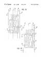
- FIG. 1provides a simplified cross-sectional view of an integrated circuit chip (or die) 10 , which includes a semiconductor layer 5 , three metal layers 1 to 3 , electrically insulating layers 7 , and passivation layer 8 .
- Semiconductor layer 5which is typically polysilicon, is used for forming the transistors and other electronic devices and also may be used for routing some of the electrical connections between these electronic devices. However, wire routing occupies space on the semiconductor layer 5 which otherwise could be used for the electronic devices. As a result, ordinarily only the shorter electrical connections are formed on semiconductor layer 5 . For the remainder of the connections, metal layers 1 to 3 are provided.
- Metal layers 1 to 3may be formed from any of a variety of materials including aluminum, copper or an electrically conductive alloy. Typically, two to four metal layers are formed on top of semiconductor layer 5 . To simplify the routing process, routing typically is performed using mainly horizontal and vertical trace (or wire) segments. Moreover, to permit such routing to be performed in an orderly manner, each metal layer typically is designated as either a horizontal metal layer or a vertical metal layer. Horizontal metal layers are used primarily for horizontal wire segments and vertical metal layers are used primarily for vertical wire segments. By routing wires in the metal layers 1 to 3 , electrical connections can be made without using valuable space on semiconductor layer 5 .
- an electrically insulating layer 7which typically is formed as an oxide film. Connections between metal layers or between the metal layers and connections between a metal layer, other than metal layer 1 , and semiconductor layer 5 are made using interlayer holes called vias. Direct contacts are made between semiconductor layer 5 and metal layer 1 .
- Passivation layer 8functions to prevent the deterioration of the electrical properties of the die caused by water, ions and other external contaminants.
- passivation layer 8is made of a scratch-resistant material such as silicon nitride and/or silicon dioxide.
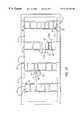
- FIG. 2provides a representational illustration of the layout of the logic portion 20 of integrated circuit die 10 .
- Logic portion 20generally is located at the interior of die 10 .
- I/O buffer cells(not shown) for interfacing with devices external to die 10 .
- logic portion 20is bordered by a power (VDD) ring 21 and a ground (VSS) ring 22 .
- VDDpower
- VSSground
- Vertical power rails 24bring power and vertical ground rails 25 bring ground to the internal logic electronic components from the power ring 21 and ground ring 22 , respectively.
- various logic cells 27are arranged in cell columns 28 , with each cell column 28 being bordered by a power rail 24 and a ground rail 25 .
- FIG. 2shows a significant gap between cell columns 28 , the actual gap may in fact be much smaller.
- Overlaying cell columns 28are channels 29 .
- each channel 29may be defined as the space from the left side of one cell column 28 to the left side of the next cell column 28 .
- Each cell 27includes one or more predetermined gates, flip-flops and/or other basic electronic devices. Also as shown in FIG. 2, each cell 27 typically has a standard width, although its length may be different from that of other cells. Although interior portion 20 is referred to herein as the logic portion of the IC and cells 27 are referred to herein as logic cells, this terminology is used merely to distinguish those cells from the 10 buffer cells. It should be understood that certain cells 27 may include some or all non-logic processing, such as analog signal processing.
- Power and ground rings 21 and 22 and power and ground rails 24 and 25usually are formed on the die's metal layers.
- vertical wire segmentsare formed on metal layers 1 and 3 and horizontal wire segments are formed on metal layer 2 .
- metal layers 1 to 3also are used for routing electrical connections for carrying signals between and within the cells 27 .
- the routing problemtypically is separated into intra-column and inter-column routing.
- intra-column routingelectrical connections are routed between electronic components in the same cell column, while in inter-column routing electrical connections are routed between cells in different cell columns.
- the routing problemis divided in this manner because the considerations involved in intra-column routing are usually different than the considerations involved in inter-column. Most of these considerations arise from the fact that a greater proportion of intra-column routing is performed over cells, as compared with inter-column routing.
- direct contactscan be formed between semiconductor layer 5 and metal layer 1 , there is no need to use vias, which typically occupy additional space, when routing over cells on metal layer 1 .
- viaswhich typically occupy additional space, when routing over cells on metal layer 1 .
- routing over cellsoften imposes additional wire spacing requirements, such as limitations on routing over noise-sensitive circuitry.
- metal layer 1initially is used for intra-column routing.
- FIG. 3Adepicts intra-column routing on metal layer 1 for a single cell column 40 .
- point-to-point routingis performed entirely on metal layer 1
- horizontal trace segments, as well as vertical trace segments,are implemented on metal layer 1 , even though metal layer 1 is designated as a vertical metal layer.
- metal layer 1 intra-column routingis performed independently of the grid used for cell placement and inter-column routing (as described below).
- electrical connectionsare routed between the pins of cells 45 , 46 and 47 , as well as internally within those cells. As shown in FIG. 3A, routing is performed in a manner which tends to make the most efficient use of metal layer 1 , independent of the grid lines.
- pin 50 of cell 46is connected to pin 52 of cell 47 using a wire trace which consists of vertical wire segment 54 A, horizontal wire segment 54 B and vertical wire segment 54 C. As indicated above, each of segments 54 A, 54 B and 54 C is implemented on metal layer 1 .
- FIG. 3Billustrates inter-column routing in this technique.
- inter-column routingis generally grid-based, meaning that the axial line of each wire segment generally is required to lie along a grid line in a predetermined, regularly spaced rectangular grid. Use of such grid-based routing often greatly simplifies the routing problem.
- the axial line of each inter-column wire segmentis coincident with one of the vertical grid lines 42 or the horizontal grid lines 43 .
- metal layers 1 and 3are vertical metal layers and metal layer 2 is a horizontal metal layer. Accordingly, the horizontal inter-column wire segments 41 are implemented using on-grid resources on metal layer 2 .
- the vertical inter-column wire segments 41are implemented using on-grid resources on metal layers 1 and 3 .
- inter-column routingis performed after metal layer 1 intra-column routing, and ordinarily there will be little if any on-grid over-the-cell resources on metal layer 1 after completion of metal layer 1 intra-column routing.
- the channel portions of metal layer 1are used in inter-column routing.
- Trace 67consists of horizontal wire segment 67 A, vertical wire segment 67 B and horizontal wire segment 67 C. Segments 67 A and 67 C are implemented on metal layer 2 , while segment 67 B is implemented on either metal layer 1 or metal layer 3 .
- this stepalso performs intra-column routing, in a similar manner to the inter-column routing, for any intra-column connections not capable of being completed in the metal layer 1 intra-column routing step described above. That is, any such pins are connected by using on-grid channel-routing. For instance, a connection is routed between pin 74 of cell 71 and pin 75 of cell 72 , both in cell column 70 , by routing a horizontal wire segment 76 A from pin 74 into adjacent channel 80 , routing a vertical wire segment 76 B in channel 80 , and then routing another horizontal wire segment 76 C to pin 75 .
- Segments 76 A and 76 Care routed on horizontal metal layer 2 and segment 76 C is routed on either vertical metal layer 1 or vertical metal layer 3 . Vias connect segment 76 A to pin 74 , segment 76 B to segment 76 A, segment 76 C to segment 76 B, and pin 75 to segment 76 C.
- the foregoing routing technique of performing intra-column routing on metal layer 1 independently of the grid and then grid-based routing for all remaining connectionsprovides good metal utilization for both over-the-cell and channel routing in many cases.
- an even more efficient metal utilization techniqueis desired.
- the conventional techniquessometimes result in a situation in which a particular cell layout can not be routed. In these situations, adjustments to cell layout generally must be made and then routing retried, thus lengthening the design process. In other cases when using such conventional techniques, the die size must be increased to provide sufficient space for wire routing, thereby increasing the cost of the resulting integrated circuit.
- the present inventionaddresses the foregoing problems by routing an electrical connection between cells in different cell columns by identifying and using an available off-grid resource within a cell column.
- the inventionis directed to routing of electrical connections between cells arranged in cell columns on an integrated circuit (IC) die. Electrical connections are routed on a routing layer between cells located in a first cell column. An identification is made of an available off-grid resource capable of being used for wire routing that is both within the first cell column and on the routing layer. An electrical connection is routed between a first cell and a second cell located in different cell columns using at least a portion of the identified available off-grid resource.
- ICintegrated circuit
- the inventionis directed to routing electrical connections between cells arranged in cell columns on an integrated circuit (IC) die. Electrical connections are routed on a routing layer between cells located in a first cell column. An identification is made of an available off-grid resource capable of being used for wire routing that is both within the first cell column and on the routing layer. An electrical connection is routed between a first cell and a second cell located in different cell columns, using grid-based routing in a channel between the first cell and the second cell and using at least a portion of the identified available off-grid resource.
- ICintegrated circuit
- the inventionmay provide a technique for routing layout designs which are not capable of being routed using certain conventional techniques. Moreover, by increasing the likelihood of obtaining a routing solution, the present invention can avoid the necessity of re-designing the layout in certain cases, thereby reducing design time and cost.
- the identified off-grid resourceis used to move a pseudo-pin generated in global routing.
- the present inventioncan provide additional routing resources frequently without significant changes to the existing routing process.
- the present inventionalso addresses the prior art problems discussed above by providing an integrated circuit die which includes an electrical connection having an on-grid wire segment in a channel and an off-grid wire segment formed in a cell column.
- the inventionis directed to an integrated circuit die which includes vertical power rails and vertical ground rails.
- Cell columnsincluding a first cell column and a second cell column, are each bordered by a vertical power rail and a vertical ground rail.
- a channelis provided between the first cell column and the second cell column.
- An electrical connectionis provided between a first electronic component in the first cell column and a second electronic component in the second cell column.
- the electrical connectionincludes an on-grid wire segment in the channel between the first cell column and the second cell column and an off-grid wire segment formed in one of the cell columns.
- an integrated circuit according to the present inventionfrequently can be both relatively easy and efficient to route.
- FIG. 1provides a cross-sectional view of an integrated circuit die.
- FIG. 2illustrates one example of layout in an integrated circuit die.
- FIGS. 3A and 3Billustrate conventional intra-column and inter-column routing techniques, respectively.
- FIG. 4is a flow diagram for explaining integrated circuit design according to a representative embodiment of the invention.
- FIG. 5is a flow diagram for explaining physical design according to a representative embodiment of the invention.
- FIG. 6is a flow diagram for explaining routing according to a representative embodiment of the invention.
- FIGS. 7A and 7Billustrate a method for identifying off-grid over-the-cell resources according to a preferred embodiment of the invention.
- FIG. 8illustrates the output of the global routing step for one net according to a representative embodiment of the invention.
- FIG. 9is a flow diagram for explaining pre-processing of the global routing output according to a preferred embodiment of the invention.
- FIG. 10illustrates one example of the pre-processing global routing output according to a preferred embodiment of the invention.
- FIG. 11is a block diagram of a general purpose computer system, representing one suitable computer platform for implementing the methods of the invention.
- FIG. 4illustrates a flow diagram for providing a brief overview of IC chip design according to a representative embodiment of the invention. Briefly, according to FIG. 4, an IC design specification is prepared; a functional description of a system corresponding to the design specification is produced; a gate-level circuit description is synthesized from the functional description; a simulation is performed to verify the feasibility of the gate-level description; and physical design is performed.
- step 100an IC design specification is prepared.
- the desired system designis described in the highest level of abstraction.
- Subsequent steps in the design cycleprovide successively more detail until all information required to fabricate the chip has been derived.
- the design specificationdictates features such as performance criteria, required external interfaces and protocols, and product cost targets.
- a functional designis produced.
- the functional designdescribes a system that will satisfy the IC design specification prepared in step 100 .
- the functional designis written using a highly structured syntax so as to permit subsequent steps in the design cycle to be performed using automated computer-aided design tools.
- the functional designis written in a hardware description language (HDL) such as VHDL (IEEE standard 1076-1993) or Verilog-HDL.
- HDLhardware description language
- a description of a gate-level circuitis synthesized based on the HDL code produced in step 102 .
- gate-level designis performed by running an automated synthesis tool on the HDL code.
- physically realizable gates and flip-flopsare selected from a pre-defined library and are interconnected in a manner so as to satisfy the relationships and to perform the processing defined by the HDL code.
- Processing by the synthesis toolpreferably utilizes pre-defined user design constraints which have been formulated in an effort to enhance the feasibility of the design, particularly with respect to problems which might otherwise not be discovered until later in the design cycle.
- the format of the gate-level circuit description synthesized in step 104is a “netlist”, which categorizes a number of “nets”, each including one or more gates and/or flip-flops, and which also describes the interconnections between these nets.
- gate-level verification step 106a computer simulation is run to test the circuit design synthesized during gate-level design step 104 . The goals of this simulation are to determine whether all performance criteria have been met and whether any timing or other circuit errors will occur in response to a variety of different input signals and conditions.
- the netlistis provided to physical design step 108 , and a dump of top-level signals in the netlist is provided to the user.
- the netlist generated in step 106is mapped to information for physically implementing the corresponding circuit on an IC die.
- the objective of physical designis to determine an optimal arrangement of devices in a plane or in a three-dimensional space, and an efficient interconnection or routing scheme between the devices to obtain the desired functionality.
- One goal of physical design step 108is to implement the design using minimum chip area. Other factors considered during physical design include thermal generation, power/ground noise, electromagnetic effects, and the number of metal layers available for wire routing.
- Step 108produces a set of design files in an unambiguous representation known as an intermediate form that describes the layout.
- the design filesare then converted into pattern generator files that are used to produce patterns called masks by an optical or electron beam pattern generator.
- a representative embodiment of physical design step 108is discussed in more detail below in connection with FIG. 5 .
- step 104a gate-level description can not be generated to satisfy the functional design requirements using the available technology library, while at the same time maintaining the user's design constraints.
- the functional descriptionmay need to be redesigned in step 102 in order to achieve a feasible design.
- FIG. 5A more detailed discussion of physical design step 108 (shown in FIG. 4) in the preferred embodiment of the invention will now be discussed with reference to the flow diagram shown in FIG. 5 .
- cellsare obtained based on the supplied netlist; I/O cells and associated bonding pads are laid out around the periphery of the die; interior logic cells and power/ground rails are laid out; traces are routed between the cells; and compaction is performed.
- step 130cell descriptions are obtained from a cell library based on the netlist input from step 106 . Specifically, logic and other signal processing cells, as well as I/O buffer cells, are obtained corresponding to the circuits identified in the netlist.
- step 132the I/O buffer cells and associated bonding pads are laid out (or placed) around the periphery of the die.
- layout or placementrefers to generating layout or placement information. During device fabrication, electronic devices and wires are formed on the IC die using the placement information generated during physical design.
- step 134the logic cells are placed at the interior of the die.
- a main concern in performing this placementis to reduce spacing between cells, thereby minimizing the amount of wire routing that will need to be performed.
- the main sub-steps in performing step 134are partitioning, floor planning and layout.
- the logic portion of a chipmay contain several million transistors. As a result, layout of the entire chip generally cannot be handled due to the limitations of available memory space and computation power. Therefore, the logic circuitry normally is partitioned by grouping circuit components into blocks, such as subcircuits and modules. The actual partitioning process considers many factors such as the size of the blocks, number of blocks and number of interconnections between the blocks.
- the output of partitioningis a set of blocks, together with the interconnections required between these blocks.
- the partitioning processis often hierarchical, although non-hierarchical (e.g. flat) processes can be used, and at the topmost level a circuit can have between 5 to 25 blocks. However, greater numbers of blocks are possible and contemplated. Each block is then partitioned recursively into smaller blocks.
- Floor planning and placementare concerned with selecting good layout alternatives for each block of the entire chip, as well as between blocks and to the edges.
- Floor planningis a critical step as it sets up the ground work for a good layout.
- the goal of placementis to find a minimum area arrangement for the blocks that allows completion of interconnections between the blocks. Placement typically is done in two phases. In the first phase, an initial placement is created. In the second phase, the initial placement is evaluated and iterative improvements are made until the layout has minimum area and conforms to design specifications.
- tracesare routed from the I/O cells and interior logic cells to other I/O and interior logic cells, as well as to power and ground rings.
- the objective of routingis to complete all the interconnections between cells and within each cell according to the specified netlist, subject to the space available for routing. Another goal of routing is to complete all circuit connections using the shortest possible wire length. Routing is discussed in more detail below in connection with FIG. 6 .
- step 138compaction is performed.
- Compactionis the process of compressing the layout in both directions such that the total area is reduced. By making the chips smaller, wire lengths are reduced, which in turn reduces the signal delay between components of the circuit. At the same time, a smaller area enables more chips to be produced on a wafer, which in turn reduces the cost of manufacturing. Compaction must ensure that no rules regarding the design and fabrication processes are violated.
- step 108While the foregoing implementation of physical design step 108 is preferable, other variations apparent to those skilled in the art may also be used. Moreover, although the steps are described above and shown in FIG. 5 as being entirely sequential, it should be understood that feasibility problems discovered in any one of the steps frequently will require repeating a prior step. For example, routing problems discovered in step 136 might require adjustments to layout by re-executing portions of step 134 .
- Trace routing step 136(shown in FIG. 5) will now be described in more detail in connection with the flow diagram shown in FIG. 6 .
- intra-column routingis performed, the die is searched for off-grid over-the-cell resources, global routing is performed, the results of global routing are pre-processed using the identified off-grid over-the-cell resources, and detailed routing is performed.
- over-the-cellmeans within a cell column.
- metal layer 1 intra-column routingis performed.
- metal layer 1 intra-column routing in the preferred embodimentutilizes metal layer 1 in an attempt to achieve an efficient routing pattern regardless of any grid used for layout or for inter-column routing.
- step 150routes horizontal, as well as vertical, wire segments on metal layer 1 .
- this stepis performed using an automated design tool such as LSI Logic's Stub Router.
- a searchis made to identify off-grid resources within a cell column that can be used for placing a wire.
- xx r - 1 2 ⁇ w r - 1 2 ⁇ w w - S m ⁇ ⁇ i ⁇ ⁇ n
- x ris the horizontal position of the center of the rail
- w ris the width of the rail
- w wis the width of the desired wire
- S minis the minimum wire-to-wire spacing requirement
- invalid positionsinclude locations where the minimum wire spacing requirement would be violated with respect to any other wire segment in the cell column or where wire segments are prohibited, such as by a route-block command included in a cell having noise-sensitive circuitry.
- any identified ranges of y which are shorter than the required minimum wire lengthare discarded. This approach is used to identify off-grid over-the-cell resources immediately inside each rail of each cell column on the die.
- FIG. 7Aillustrates a cell column 180 bordered by a power rail 181 and a ground rail 182 .
- an x position 185is determined with respect to rail 181 and an x position 186 is determined with respect to rail 182 .
- x position 185is the minimum spacing from rail 181 at which a wire could be placed without violating the minimum spacing requirement from rail 181 .
- x position 186is the minimum spacing from rail 182 at which a wire could be placed without violating the minimum spacing requirement from rail 182 .
- the valid y positionsare determined for each of x positions 185 and 186 .
- step 154global routing is performed for any pins not connected in step 150 , i.e., all pins used for inter-column connections and any intra-column connection pins which were not connected in step 150 .
- global routingdisregards the exact geometric details of each wire and terminal and instead merely finds a list of channels that are to be used as a passageway for each wire. In other words, global routing specifies the loose route of a wire through different regions of the routing space.
- Various techniques exist for performing global routingand are well documented in the art, such as Steiner Tree based techniques and hierarchical techniques.
- the output of global routing step 154is a set of pseudo-pins which act as guides for the subsequent step of detailed routing. More preferably, global routing step 154 specifies a pseudo-pin for each cell column between the cell column containing the first pin to be connected and the cell column containing the second pin to be connected. FIG. 8 illustrates the output of this step.
- FIG. 8shows an example of two pins to be connected, pin 201 on cell 200 and pin 211 on cell 210 .
- pseudo-pins 221 and 225are specified.
- pseudo-pin 221is on the border between channel 241 and channel 242 ; similarly, pseudo-pin 25 is on the border between channels 242 and 243 .
- a detailed routercould attempt to complete the connections between pins 201 and 211 by routing a connection between pin 201 and pseudo-pin 221 in channel 241 , a connection between pseudo-pin 221 and pseudo-pin 225 in channel 242 , and a connection pseudo-pin 225 and pin 211 in channel 243 .
- Also shown in FIG. 8are off-grid over-the-cell metal layer 1 resources 251 to 275 which were identified in step 152 .
- step 156the output of the global router is pre-processed using the resources identified in step 152 , so as to simplify the task of the detailed router.
- this pre-processinginvolves using those resources to effectively move the pseudo-pins output by the global router so that the required in-channel routing by the detailed router is reduced.
- the identified off-grid over-the-cell resourcesare used to move the pins or pseudo-pins in each channel closer together, thereby simplifying the total routing length required to be performed by the detailed router.
- the term “pin”is meant to include pseudo-pins as well as cell pins.
- FIG. 9illustrates a flow diagram for explaining a method for performing step 156 with respect to two pins to be connected, where the starting pin is a pin on the left side of the die and the ending pin is a pin on the right side of the die.
- the starting pinis selected; the current pin is checked to determine whether it is adjacent to an available off-grid over-the-cell resource; if so, an attempt is made to move the current pin; the foregoing process is then repeated for each successive pin up to and including the ending pin.
- step 300the starting pin initially is selected as the current pin.
- step 302it is determined whether the current pin is adjacent to an available off-grid over-the-cell resource identified in step 152 . If so, processing proceeds to step 304 ; otherwise, processing skips to step 320 .
- the current pinis adjacent to an available off-grid over-the-cell resource if there is such a resource in the corresponding cell column at the same vertical position as the current pin.
- the corresponding cell columngenerally will be the cell column in which the current pin is located or the cell column to the immediate right of the current pin, in the event the current pin is a pseudo-pin.
- step 304an attempt is made to move the current pin vertically toward the starting pin by routing on the available off-grid over-the-cell resources adjacent to the current pin.
- the current pinis not moved farther than the previous pin. For instance, if the starting pin is vertically higher than the current pin and the off-grid over-the-cell resource extends vertically up, then a wire is routed in the available over-the-cell resources, so as to move the current pin higher, to a point which is the lower of the starting pin and the previous pin.
- step 306an attempt is made to move the current pin vertically toward the ending pin by routing a wire on the available off-grid over-the-cell resource adjacent to the current pin.
- the movement of the next pinis limited to a vertical position not beyond the pin following the next pin.
- the ending pinis lower than the current pin and if the off-grid over-the-cell resource extends downward, the current pin is moved downward to a point which is the higher of the ending pin and the pin following the current pin.
- the current pinmay have been moved in either zero, one or two directions. If no movement has been performed, then the current pin remains unchanged. If the current pin has been moved in one direction, then two pins result: the current pin and the current pin as moved, with these two pins connected by a wire segment routed on at least one available off-grid over-the-cell track. Both such pins will be provided to the detailed router. If the current pin has been moved in two directions, two new pins result: the current pin as moved in each direction, with these two new pins connected by a wire segment routed on at least one available off-grid over-the-cell track. Both such new pins will be provided to the detailed router in place of the current pin.
- step 308it is determined whether the current pin is the ending pin. If not, processing proceeds first to step 320 to select the next pin as the current pin and then to step 302 to repeat the process for the new current pin. In this embodiment, pins are processed in the order from left to right; accordingly, the next pin is the first pin to the right of the current pin. If the current pin is the ending pin, then step 156 is completed.
- FIG. 10illustrates the global routing output shown in FIG. 8 after pre-processing as described above.
- each of the pins 201 , 221 , 223 , 225 , 227 and 211have been processed in sequence.
- the dieuses three metal layers, metal layers 1 to 3 .
- Starting pin 201is not adjacent to an off-grid over-the-cell resource, and therefore is not moved.
- Pseudo-pin 221is adjacent to resource 259 and resource 259 extends both upward and downward from pseudo-pin 221 . Therefore, in step 304 pseudo-pin 221 is moved up to position 221 A.
- the pseudo-pinsWhen using a three metal layer die, the pseudo-pins typically will be located on metal layer 2 , the horizontal metal layer. Accordingly, a horizontal wire 279 is routed on metal layer 2 from pseudo-pin 221 into cell column 246 , to a position just inside of (to the right of) the x position for the available off-grid over-the-cell resource. A via is then inserted to connect metal layer 2 to metal layer 1 at this point. It is noted that it is typically necessary to go slightly inside of the x position of the off-grid over-the-cell resource because a via typically is wider than a wire.
- a viacan be placed at any position along each identified off-grid over-the-cell resource without violating a spacing requirement.
- thiswill not always be true because the identification in step 152 only required that the resources be capable of containing a wire, which generally will be narrower than via.
- the length of a particular wire routed on the off-grid over-the-cell resourcemay need to be shortened until a suitable location is found for a via.
- the next pseudo-pin 225is adjacent to resource 266 . Because resource 266 extends upward, pseudo-pin 225 can be moved upward in a manner similar to pin 221 above. However, the upward movement of pin 225 is limited to the vertical position of previous pseudo-pin 221 B, i.e., to position 225 A.
- Resources 266 and 269extend downward from current pseudo-pin 225 ; accordingly, pseudo-pin 225 is moved downward by routing wires on resources 266 and 269 , together with a horizontal wire segment 280 (such as on metal layer 2 ) to a position 225 B.
- ending pin 211is on the left side of cell column 248 , and is adjacent to resource 273 which extends upward. Therefore, pin 211 is moved to new position 211 A by routing a wire on resource 273 .
- the final output of step 156 in this exampleincludes pins 201 , 221 A, 221 B, 225 A, 225 B and 211 A.
- the pins to be connected within a channelare moved closer together.
- pseudo-pin 221has been moved to position 221 A which is vertically closer to pin 201 .
- pin 221also has been moved to position 221 B and pin 225 has been moved to position 225 A, eliminating all vertical distance between the two.
- step 158detailed routing is performed. Detailed routing completes point-to-point connections between terminals on the cells using the information provided by the global routing step 154 , as modified by the pre-processing step 156 . Specifically, the loose routing is converted into exact routing by specifying the geometric information such as width of wires and their layer assignments. In the preferred embodiment, this is accomplished by routing connections between the pairs of pins in each channel for each net. Techniques for detailed routing between pairs of points within the same channel are well known in the art. Thus, with reference to the net shown in FIG.
- pin 201is connected to pseudo-pin 221 A in channel 241
- pin 221 Bis connected to pin 225 A in channel 242
- pin 225 Bis connected to pin 211 A in channel 243 . Because each such pair of pins is closer than the original output of global routing step 154 , the task of detailed routing in step 158 requires less vertical routing and generally will be more likely to result in a valid solution.
- the foregoing embodimentprovides one example of a method for identifying and using off-grid over-the-cell resources.
- the identification of off-grid over-the-cell resources in step 152may be performed after global routing step 154 , rather than before.
- pinsare moved using off-grid over-the-cell resources.
- the inventioncan be implemented without significant changes to either the global routing step or the detailed routing step. It is noted that both of these steps generally are performed using computer-aided design tools, and therefore it is highly advantageous to improve routing without modifying these tools.
- the pre-processing step 156could be eliminated and the identified off-grid over-the-cell resources supplied directly to the detailed routing step 158 , which in turn would directly use these resources when routing connections.
- the integrated circuitcan be fabricated using the masks generated in step 108 (shown in FIG. 4 ), but otherwise employing conventional fabrication techniques.
- the masks generated in step 108are used to pattern a silicon wafer using a sequence of photolithographic steps.
- Photolithographyis a common technique employed in the manufacture of semiconductor devices.
- a semiconductor waferis coated with a layer (film) of light-sensitive material, such as photoresist.
- the waferis exposed to projected light, typically actinic light, which manifests a photochemical effect on the photoresist, which is subsequently chemically etched, leaving a pattern of photoresist “lines” on the wafer corresponding to the pattern on the mask.
- projected lighttypically actinic light
- waferis a thin piece of semiconductor material from which semiconductor chips are made.
- the four basic operations utilized to fabricate wafersinclude (1) layering, (2) patterning, (3) doping and (4) heat treatments.
- the layering operationadds thin layers of material, including insulators, semiconductors, and conductors, to a wafer surface. During the layering operation, layers are either grown or deposited. Oxidation typically involves growing a silicon dioxide (an insulator) layer on a silicon wafer.
- Deposition techniquesinclude, for example, chemical vapor deposition, evaporation, and sputtering. Semiconductors are generally deposited by chemical vapor deposition, while conductors are generally deposited with evaporation or sputtering.
- Patterninginvolves the removal of selected portions of surface layers. After material is removed, the wafer surface has a pattern. The material removed may form a hole or an island.
- the process of patterningis also known to those skilled in the relevant art as microlithography, photolithography, photomasking and masking.
- the patterning operationserves to create parts of the semiconductor device on the wafer surface in the dimensions required by the circuit design and to locate the parts in their proper location on the wafer surface.
- Dopinginvolves implanting dopants in the surface of the wafer through openings in the layers to create the n-type and p-type pockets needed to form the N-P junctions for operation of discrete elements such as transistors and diodes. Doping generally is achieved with thermal diffusion (wafer is heated and exposed to the desired dopant) and ion implantation (dopant atoms are ionized, accelerated to high velocities and implanted into the wafer surface).
- FIG. 11is a block diagram of a general purpose computer system, representing one of many suitable computer platforms for implementing the methods described above.
- FIG. 11shows a general purpose computer system 450 in accordance with the present invention.
- computer system 450includes a central processing unit (CPU) 452 , read-only memory (ROM) 454 , random access memory (RAM) 456 , expansion RAM 458 , input/output (I/O) circuitry 460 , display assembly 462 , input device 464 , and expansion bus 466 .
- Computer system 450may also optionally include a mass storage unit 468 such as a disk drive unit or nonvolatile memory such as flash memory and a real-time clock 470 .
- CPU 452is coupled to ROM 454 by a data bus 472 , control bus 474 , and address bus 476 .
- ROM 454contains the basic operating system for the computer system 450 .
- CPU 452is also connected to RAM 456 by busses 472 , 474 , and 476 .
- Expansion RAM 458is optionally coupled to RAM 456 for use by CPU 452 .
- CPU 452is also coupled to the I/O circuitry 460 by data bus 472 , control bus 474 , and address bus 476 to permit data transfers with peripheral devices.
- I/O circuitry 460typically includes a number of latches, registers and direct memory access (DMA) controllers. The purpose of I/O circuitry 460 is to provide an interface between CPU 452 and such peripheral devices as display assembly 462 , input device 464 , and mass storage 468 .
- DMAdirect memory access
- Display assembly 462 of computer system 450is an output device coupled to I/O circuitry 460 by a data bus 478 .
- Display assembly 462receives data from I/O circuitry 460 via bus 478 and displays that data on a suitable screen.
- the screen for display assembly 462can be a device that uses a cathode-ray tube (CRT), liquid crystal display (LCD), or the like, of the types commercially available from a variety of manufacturers.
- Input device 464can be a keyboard, a mouse, a stylus working in cooperation with a position-sensing display, or the like.
- the aforementioned input devicesare available from a variety of vendors and are well known in the art.
- mass storage 468is generally considered desirable. However, mass storage 468 can be eliminated by providing a sufficient mount of RAM 456 and expansion RAM 458 to store user application programs and data. In that case, RAMs 456 and 458 can optionally be provided with a backup battery to prevent the loss of data even when computer system 450 is turned off. However, it is generally desirable to have some type of long term mass storage 468 such as a commercially available hard disk drive, nonvolatile memory such as flash memory, battery backed RAM, PC-data cards, or the like.
- a removable storage read/write device 469may be coupled to I/O circuitry 460 to read from and to write to a removable storage media 471 .
- Removable storage media 471may represent, for example, a magnetic disk, a magnetic tape, an opto-magnetic disk, an optical disk, or the like. Instructions for implementing the inventive method may be provided, in one embodiment, to a network via such a removable storage media.
- CPU 452In operation, information is input into the computer system 450 by typing on a keyboard, manipulating a mouse or trackball, or “writing” on a tablet or on position-sensing screen of display assembly 462 .
- CPU 452then processes the data under control of an operating system and an application program, such as a program to perform steps of the inventive method described above, stored in ROM 454 and/or RAM 456 .
- CPU 452then typically produces data which is output to the display assembly 462 to produce appropriate images on its screen.
- Expansion bus 466is coupled to data bus 472 , control bus 474 , and address bus 476 . Expansion bus 466 provides extra ports to couple devices such as network interface circuits, modems, display switches, microphones, speakers, etc. to CPU 452 . Network communication is accomplished through the network interface circuit and an appropriate network.
- Suitable computers for use in implementing the present inventionmay be obtained from various vendors. Various computers, however, may be used depending upon the size and complexity of the OPC tasks. Suitable computers include mainframe computers, multiprocessor computers, workstations or personal computers. In addition, although a general purpose computer system has been described above, a special-purpose computer may also be used.
- the present inventionalso relates to machine readable media on which are stored program instructions for performing the methods of this invention.
- Such mediaincludes, by way of example, magnetic disks, magnetic tape, optically readable media such as CD ROMs, semiconductor memory such as PCMCIA cards, etc.
- the mediummay take the form of a portable item such as a small disk, diskette, cassette, etc., or it may take the form of a relatively larger or immobile item such as a hard disk drive or RAM provided in a computer.
Landscapes
- Design And Manufacture Of Integrated Circuits (AREA)
- Semiconductor Integrated Circuits (AREA)
Abstract
Description


Claims (14)
Priority Applications (2)
| Application Number | Priority Date | Filing Date | Title |
|---|---|---|---|
| US09/183,292US6174742B1 (en) | 1998-10-30 | 1998-10-30 | Off-grid metal layer utilization |
| US09/693,014US6338972B1 (en) | 1998-10-30 | 2000-10-20 | Off-grid metal layer utilization |
Applications Claiming Priority (1)
| Application Number | Priority Date | Filing Date | Title |
|---|---|---|---|
| US09/183,292US6174742B1 (en) | 1998-10-30 | 1998-10-30 | Off-grid metal layer utilization |
Related Child Applications (1)
| Application Number | Title | Priority Date | Filing Date |
|---|---|---|---|
| US09/693,014DivisionUS6338972B1 (en) | 1998-10-30 | 2000-10-20 | Off-grid metal layer utilization |
Publications (1)
| Publication Number | Publication Date |
|---|---|
| US6174742B1true US6174742B1 (en) | 2001-01-16 |
Family
ID=22672221
Family Applications (2)
| Application Number | Title | Priority Date | Filing Date |
|---|---|---|---|
| US09/183,292Expired - LifetimeUS6174742B1 (en) | 1998-10-30 | 1998-10-30 | Off-grid metal layer utilization |
| US09/693,014Expired - LifetimeUS6338972B1 (en) | 1998-10-30 | 2000-10-20 | Off-grid metal layer utilization |
Family Applications After (1)
| Application Number | Title | Priority Date | Filing Date |
|---|---|---|---|
| US09/693,014Expired - LifetimeUS6338972B1 (en) | 1998-10-30 | 2000-10-20 | Off-grid metal layer utilization |
Country Status (1)
| Country | Link |
|---|---|
| US (2) | US6174742B1 (en) |
Cited By (37)
| Publication number | Priority date | Publication date | Assignee | Title |
|---|---|---|---|---|
| US20040033685A1 (en)* | 2002-08-16 | 2004-02-19 | Taiwan Semiconductor Manufacturing Company | Aluminum/copper clad interconnect layer for VLSI applications |
| US6710366B1 (en) | 2001-08-02 | 2004-03-23 | Ultradots, Inc. | Nanocomposite materials with engineered properties |
| US20080120588A1 (en)* | 2005-06-27 | 2008-05-22 | Becker Scott T | Methods for Creating Primitive Constructed Standard Cells |
| US7398280B1 (en)* | 2003-06-24 | 2008-07-08 | Altera Corporation | Method and system for manufacturing integrated circuits meeting special customer requirements with multiple subcontractors in remote locations |
| US20080222587A1 (en)* | 2007-03-05 | 2008-09-11 | Tela Innovations, Inc. | Integrated Circuit Cell Library for Multiple Patterning |
| US7446352B2 (en) | 2006-03-09 | 2008-11-04 | Tela Innovations, Inc. | Dynamic array architecture |
| US20090032898A1 (en)* | 2007-08-02 | 2009-02-05 | Tela Innovations, Inc. | Methods for Defining Dynamic Array Section with Manufacturing Assurance Halo and Apparatus Implementing the Same |
| US20090100396A1 (en)* | 2007-02-20 | 2009-04-16 | Tela Innovations, Inc. | Methods and Systems for Process Compensation Technique Acceleration |
| US20090108360A1 (en)* | 2007-10-26 | 2009-04-30 | Tela Innovations, Inc. | Methods, structures and designs for self-aligning local interconnects used in integrated circuits |
| US20090152734A1 (en)* | 2007-12-13 | 2009-06-18 | Tela Innovations, Inc. | Super-Self-Aligned Contacts and Method for Making the Same |
| US7577049B1 (en) | 2006-08-08 | 2009-08-18 | Tela Innovations, Inc. | Speculative sense enable tuning apparatus and associated methods |
| US20090224408A1 (en)* | 2008-03-27 | 2009-09-10 | Tela Innovations, Inc. | Methods for Multi-Wire Routing and Apparatus Implementing Same |
| US20090228853A1 (en)* | 2006-03-09 | 2009-09-10 | Tela Innovations, Inc. | Methods for Defining Contact Grid in Dynamic Array Architecture |
| US20090228857A1 (en)* | 2008-01-31 | 2009-09-10 | Tela Innovations, Inc. | Enforcement of Semiconductor Structure Regularity for Localized Transistors and Interconnect |
| US20090224396A1 (en)* | 2006-03-09 | 2009-09-10 | Becker Scott T | Oversized Contacts and Vias in Semiconductor Chip Defined by Linearly Constrained Topology |
| US20090224317A1 (en)* | 2008-03-13 | 2009-09-10 | Tela Innovations, Inc. | Cross-Coupled Transistor Layouts in Restricted Gate Level Layout Architecture |
| US7590968B1 (en) | 2006-03-01 | 2009-09-15 | Tela Innovations, Inc. | Methods for risk-informed chip layout generation |
| US20090271753A1 (en)* | 2007-08-02 | 2009-10-29 | Tela Innovations. Inc. | Methods for Cell Phasing and Placement in Dynamic Array Architecture and Implementation of the Same |
| US20090283915A1 (en)* | 2006-03-09 | 2009-11-19 | Becker Scott T | Oversized Contacts and Vias in Layout Defined by Linearly Constrained Topology |
| US20090300575A1 (en)* | 2006-03-09 | 2009-12-03 | Stephen Kornachuk | Optimizing Layout of Irregular Structures in Regular Layout Context |
| US20090300574A1 (en)* | 2006-03-09 | 2009-12-03 | Brian Reed | Methods for Defining and Utilizing Sub-Resolution Features in Linear Topology |
| US20090294981A1 (en)* | 2006-03-09 | 2009-12-03 | Tela Innovations, Inc. | Methods for Defining and Using Co-Optimized Nanopatterns for Integrated Circuit Design and Apparatus Implementing Same |
| US20100006901A1 (en)* | 2006-03-09 | 2010-01-14 | Tela Innovations, Inc. | Semiconductor Device Portion Having Gate Electrode Conductive Structures Formed from Rectangular Shaped Gate Electrode Layout Features Defined Along At Least Four Gate Electrode Tracks and Having Corresponding Non-Symmetric Diffusion Regions |
| US20100031211A1 (en)* | 2008-08-01 | 2010-02-04 | Tela Innovations, Inc. | Methods for Controlling Microloading Variation in Semiconductor Wafer Layout and Fabrication |
| US20100277202A1 (en)* | 2006-03-09 | 2010-11-04 | Tela Innovations, Inc. | Circuitry and Layouts for XOR and XNOR Logic |
| US20100287518A1 (en)* | 2009-05-06 | 2010-11-11 | Tela Innovations, Inc. | Cell Circuit and Layout with Linear Finfet Structures |
| US20100306719A1 (en)* | 2007-02-20 | 2010-12-02 | Tela Innovations, Inc. | Integrated Circuit Cell Library with Cell-Level Process Compensation Technique (PCT) Application and Associated Methods |
| US20110084312A1 (en)* | 2009-10-13 | 2011-04-14 | Tela Innovations, Inc. | Methods for Cell Boundary Encroachment and Layouts Implementing the Same |
| US7932545B2 (en) | 2006-03-09 | 2011-04-26 | Tela Innovations, Inc. | Semiconductor device and associated layouts including gate electrode level region having arrangement of six linear conductive segments with side-to-side spacing less than 360 nanometers |
| US20110095816A1 (en)* | 2009-10-28 | 2011-04-28 | Kalray | Network on chip building bricks |
| EP2530466A1 (en) | 2002-03-30 | 2012-12-05 | Xenotope Diagnostics, Inc. | Method and device for trichomonas detection |
| US8658542B2 (en) | 2006-03-09 | 2014-02-25 | Tela Innovations, Inc. | Coarse grid design methods and structures |
| US8839175B2 (en) | 2006-03-09 | 2014-09-16 | Tela Innovations, Inc. | Scalable meta-data objects |
| US8863063B2 (en) | 2009-05-06 | 2014-10-14 | Tela Innovations, Inc. | Finfet transistor circuit |
| US9035359B2 (en) | 2006-03-09 | 2015-05-19 | Tela Innovations, Inc. | Semiconductor chip including region including linear-shaped conductive structures forming gate electrodes and having electrical connection areas arranged relative to inner region between transistors of different types and associated methods |
| US9159627B2 (en) | 2010-11-12 | 2015-10-13 | Tela Innovations, Inc. | Methods for linewidth modification and apparatus implementing the same |
| EP3270414A1 (en)* | 2016-07-12 | 2018-01-17 | ATI Technologies ULC | Integrated circuit implementing standard cells with metal layer segments extending out of cell boundary |
Families Citing this family (6)
| Publication number | Priority date | Publication date | Assignee | Title |
|---|---|---|---|---|
| US6388332B1 (en)* | 1999-08-10 | 2002-05-14 | Philips Electronics North America Corporation | Integrated circuit power and ground routing |
| EP1489534A3 (en)* | 2003-06-20 | 2005-08-17 | Interuniversitair Microelektronica Centrum Vzw | A resource activity aware system for determining a resource interconnection pattern within an essentially digital device |
| US7464356B2 (en)* | 2005-12-15 | 2008-12-09 | International Business Machines Corporation | Method and apparatus for diffusion based cell placement migration |
| US8037441B2 (en)* | 2007-09-25 | 2011-10-11 | International Business Machines Corporation | Gridded-router based wiring on a non-gridded library |
| US9684754B2 (en)* | 2015-10-02 | 2017-06-20 | Arm Limited | Standard cell architecture layout |
| US10783313B2 (en) | 2018-08-30 | 2020-09-22 | Taiwan Semiconductor Manufacturing Company Ltd. | Method for improved cut metal patterning |
Citations (3)
| Publication number | Priority date | Publication date | Assignee | Title |
|---|---|---|---|---|
| US5587923A (en)* | 1994-09-07 | 1996-12-24 | Lsi Logic Corporation | Method for estimating routability and congestion in a cell placement for integrated circuit chip |
| US5870313A (en)* | 1994-04-19 | 1999-02-09 | Lsi Logic Corporation | Optimization processing for integrated circuit physical design automation system using parallel moving windows |
| US5980093A (en)* | 1996-12-04 | 1999-11-09 | Lsi Logic Corporation | Integrated circuit layout routing using multiprocessing |
Family Cites Families (2)
| Publication number | Priority date | Publication date | Assignee | Title |
|---|---|---|---|---|
| US6225143B1 (en)* | 1998-06-03 | 2001-05-01 | Lsi Logic Corporation | Flip-chip integrated circuit routing to I/O devices |
| US6182272B1 (en)* | 1998-07-16 | 2001-01-30 | Lsi Logic Corporation | Metal layer assignment |
- 1998
- 1998-10-30USUS09/183,292patent/US6174742B1/ennot_activeExpired - Lifetime
- 2000
- 2000-10-20USUS09/693,014patent/US6338972B1/ennot_activeExpired - Lifetime
Patent Citations (3)
| Publication number | Priority date | Publication date | Assignee | Title |
|---|---|---|---|---|
| US5870313A (en)* | 1994-04-19 | 1999-02-09 | Lsi Logic Corporation | Optimization processing for integrated circuit physical design automation system using parallel moving windows |
| US5587923A (en)* | 1994-09-07 | 1996-12-24 | Lsi Logic Corporation | Method for estimating routability and congestion in a cell placement for integrated circuit chip |
| US5980093A (en)* | 1996-12-04 | 1999-11-09 | Lsi Logic Corporation | Integrated circuit layout routing using multiprocessing |
Cited By (307)
| Publication number | Priority date | Publication date | Assignee | Title |
|---|---|---|---|---|
| US6710366B1 (en) | 2001-08-02 | 2004-03-23 | Ultradots, Inc. | Nanocomposite materials with engineered properties |
| EP2530466A1 (en) | 2002-03-30 | 2012-12-05 | Xenotope Diagnostics, Inc. | Method and device for trichomonas detection |
| US6777318B2 (en)* | 2002-08-16 | 2004-08-17 | Taiwan Semiconductor Manufacturing Company | Aluminum/copper clad interconnect layer for VLSI applications |
| US20040033685A1 (en)* | 2002-08-16 | 2004-02-19 | Taiwan Semiconductor Manufacturing Company | Aluminum/copper clad interconnect layer for VLSI applications |
| US7398280B1 (en)* | 2003-06-24 | 2008-07-08 | Altera Corporation | Method and system for manufacturing integrated circuits meeting special customer requirements with multiple subcontractors in remote locations |
| US20080120588A1 (en)* | 2005-06-27 | 2008-05-22 | Becker Scott T | Methods for Creating Primitive Constructed Standard Cells |
| US7917885B2 (en) | 2005-06-27 | 2011-03-29 | Tela Innovations, Inc. | Methods for creating primitive constructed standard cells |
| US7590968B1 (en) | 2006-03-01 | 2009-09-15 | Tela Innovations, Inc. | Methods for risk-informed chip layout generation |
| US9240413B2 (en) | 2006-03-09 | 2016-01-19 | Tela Innovations, Inc. | Methods, structures, and designs for self-aligning local interconnects used in integrated circuits |
| US20100019287A1 (en)* | 2006-03-09 | 2010-01-28 | Tela Innovations, Inc. | Cell of Semiconductor Device Having Sub-193 Nanometers-Sized Gate Electrode Conductive Structures Formed from Linear Shaped Gate Electrode Layout Features Defined Along At Least Four Gate Electrode Tracks with Minimum End-to-End Spacing |
| US8448102B2 (en) | 2006-03-09 | 2013-05-21 | Tela Innovations, Inc. | Optimizing layout of irregular structures in regular layout context |
| US8653857B2 (en) | 2006-03-09 | 2014-02-18 | Tela Innovations, Inc. | Circuitry and layouts for XOR and XNOR logic |
| US10230377B2 (en) | 2006-03-09 | 2019-03-12 | Tela Innovations, Inc. | Circuitry and layouts for XOR and XNOR logic |
| US10217763B2 (en) | 2006-03-09 | 2019-02-26 | Tela Innovations, Inc. | Semiconductor chip having region including gate electrode features of rectangular shape on gate horizontal grid and first-metal structures of rectangular shape on at least eight first-metal gridlines of first-metal vertical grid |
| US8264009B2 (en) | 2006-03-09 | 2012-09-11 | Tela Innovations, Inc. | Semiconductor device with linearly restricted gate level region including four transistors of first type and four transistors of second type with gate defining shapes of different length |
| US8264007B2 (en) | 2006-03-09 | 2012-09-11 | Tela Innovations, Inc. | Semiconductor device including at least six transistor forming linear shapes including at least two different gate contact connection distances |
| US10186523B2 (en) | 2006-03-09 | 2019-01-22 | Tela Innovations, Inc. | Semiconductor chip having region including gate electrode features formed in part from rectangular layout shapes on gate horizontal grid and first-metal structures formed in part from rectangular layout shapes on at least eight first-metal gridlines of first-metal vertical grid |
| US20090228853A1 (en)* | 2006-03-09 | 2009-09-10 | Tela Innovations, Inc. | Methods for Defining Contact Grid in Dynamic Array Architecture |
| US10141334B2 (en) | 2006-03-09 | 2018-11-27 | Tela Innovations, Inc. | Semiconductor chip including region having rectangular-shaped gate structures and first-metal structures |
| US20090224396A1 (en)* | 2006-03-09 | 2009-09-10 | Becker Scott T | Oversized Contacts and Vias in Semiconductor Chip Defined by Linearly Constrained Topology |
| US10141335B2 (en) | 2006-03-09 | 2018-11-27 | Tela Innovations, Inc. | Semiconductor CIP including region having rectangular-shaped gate structures and first metal structures |
| US8264008B2 (en) | 2006-03-09 | 2012-09-11 | Tela Innovations, Inc. | Semiconductor device including transistor forming linear shapes including gate portions and extending portions of different size |
| US8658542B2 (en) | 2006-03-09 | 2014-02-25 | Tela Innovations, Inc. | Coarse grid design methods and structures |
| US20090283915A1 (en)* | 2006-03-09 | 2009-11-19 | Becker Scott T | Oversized Contacts and Vias in Layout Defined by Linearly Constrained Topology |
| US20100277202A1 (en)* | 2006-03-09 | 2010-11-04 | Tela Innovations, Inc. | Circuitry and Layouts for XOR and XNOR Logic |
| US20090300574A1 (en)* | 2006-03-09 | 2009-12-03 | Brian Reed | Methods for Defining and Utilizing Sub-Resolution Features in Linear Topology |
| US20090294981A1 (en)* | 2006-03-09 | 2009-12-03 | Tela Innovations, Inc. | Methods for Defining and Using Co-Optimized Nanopatterns for Integrated Circuit Design and Apparatus Implementing Same |
| US20100001321A1 (en)* | 2006-03-09 | 2010-01-07 | Tela Innovations, Inc. | Semiconductor Device Layout Having Restricted Layout Region Including Rectangular Shaped Gate Electrode Layout Features Defined Along At Least Four Gate Electrode Tracks with Corresponding Non-Symmetric Diffusion Regions |
| US20100011330A1 (en)* | 2006-03-09 | 2010-01-14 | Tela Innovations, Inc. | Semiconductor Device Layout Having Restricted Layout Region Including Linear Shaped Gate Electrode Layout Features Defined Along At Least Four Gate Electrode Tracks with Minimum End-to-End Spacing with Corresponding Non-Symmetric Diffusion Regions |
| US20100006950A1 (en)* | 2006-03-09 | 2010-01-14 | Tela Innovations, Inc. | Semiconductor Device Portion Having Gate Electrode Conductive Structures Formed from Rectangular Shaped Gate Electrode Layout Features and Having At Least Eight Transistors |
| US20100011332A1 (en)* | 2006-03-09 | 2010-01-14 | Tela Innovations, Inc. | Semiconductor Device Layout Having Restricted Layout Region Including Linear Shaped Gate Electrode Layout Features Defined with Minimum End-to-End Spacing and Equal Number of PMOS and NMOS Transistors |
| US20100006902A1 (en)* | 2006-03-09 | 2010-01-14 | Tela Innovations, Inc. | Semiconductor Device Portion Having Sub-Wavelength-Sized Gate Electrode Conductive Structures Formed from Rectangular Shaped Gate Electrode Layout Features Defined Along At Least Four Gate Electrode Tracks and Having Corresponding Non-Symmetric Diffusion Regions |
| US20100006899A1 (en)* | 2006-03-09 | 2010-01-14 | Tela Innovations, Inc. | Semiconductor Device Portion Having Gate Electrode Conductive Structures Formed from Rectangular Shaped Gate Electrode Layout Features and Having Equal Number of PMOS and NMOS Transistors |
| US20100006948A1 (en)* | 2006-03-09 | 2010-01-14 | Tela Innovations, Inc. | Semiconductor Device Portion Having Sub-193 Nanometers -Sized Gate Electrode Conductive Structures Formed from Rectangular Shaped Gate Electrode Layout Features and Having At Least Eight Transistors |
| US20100011329A1 (en)* | 2006-03-09 | 2010-01-14 | Tela Innovations, Inc. | Semiconductor Device Layout Including Cell Layout Having Restricted Gate Electrode Level Layout with Rectangular Shaped Gate Electrode Layout Features and Equal Number of PMOS and NMOS Transistors |
| US20100006897A1 (en)* | 2006-03-09 | 2010-01-14 | Tela Innovations. Inc. | Semiconductor Device Layout Having Restricted Layout Region Including Rectangular Shaped Gate Electrode Layout Features and Equal Number of PMOS and NMOS Transistors |
| US20100006903A1 (en)* | 2006-03-09 | 2010-01-14 | Tela Innovations, Inc. | Semiconductor Device Portion Having Sub-193 Nanometers-Sized Gate Electrode Conductive Structures Formed from Rectangular Shaped Gate Electrode Layout Features Defined Along At Least Four Gate Electrode Tracks and Having Corresponding Non-Symmetric Diffusion Regions |
| US20100006901A1 (en)* | 2006-03-09 | 2010-01-14 | Tela Innovations, Inc. | Semiconductor Device Portion Having Gate Electrode Conductive Structures Formed from Rectangular Shaped Gate Electrode Layout Features Defined Along At Least Four Gate Electrode Tracks and Having Corresponding Non-Symmetric Diffusion Regions |
| US20100011331A1 (en)* | 2006-03-09 | 2010-01-14 | Tela Innovations, Inc. | Semiconductor Device Layout Including Cell Layout Having Restricted Gate Electrode Level Layout with Linear Shaped Gate Electrode Layout Features Defined Along At Least Four Gate Electrode Tracks with Minimum End-to-End Spacing with Corresponding Non-Symmetric Diffusion Regions |
| US20100006947A1 (en)* | 2006-03-09 | 2010-01-14 | Tela Innovations, Inc. | Semiconductor Device Portion Having Sub-Wavelength-Sized Gate Electrode Conductive Structures Formed from Rectangular Shaped Gate Electrode Layout Features and Having At Least Eight Transistors |
| US20100017770A1 (en)* | 2006-03-09 | 2010-01-21 | Tela Innovations, Inc. | Layout of Cell of Semiconductor Device Having Rectangular Shaped Gate Electrode Layout Features and Equal Number of PMOS and NMOS Transistors with Corresponding p-type and n-type Diffusion Regions Separated by Central Inactive Region |
| US20100012986A1 (en)* | 2006-03-09 | 2010-01-21 | Tela Innovations, Inc. | Cell of Semiconductor Device Having Gate Electrode Conductive Structures Formed from Rectangular Shaped Gate Electrode Layout Features and Equal Number of PMOS and NMOS Transistors |
| US20100017767A1 (en)* | 2006-03-09 | 2010-01-21 | Tela Innovations, Inc. | Layout of Cell of Semiconductor Device Having Rectangular Shaped Gate Electrode Layout Features Defined Along At Least Four Gate Electrode Tracks |
| US20100017768A1 (en)* | 2006-03-09 | 2010-01-21 | Tela Innovations, Inc. | Layout of Cell of Semiconductor Device Having Rectangular Shaped Gate Electrode Layout Features Defined Along At Least Four Gate Electrode Tracks with Corresponding p-type and n-type Diffusion Regions Separated by Central Inactive Region |
| US20100012984A1 (en)* | 2006-03-09 | 2010-01-21 | Tela Innovations, Inc. | Semiconductor Device Portion Having Sub-Wavelength-Sized Gate Electrode Conductive Structures Formed from Linear Shaped Gate Electrode Layout Features Defined with Minimum End-to-End Spacing and Having Equal Number of PMOS and NMOS Transistors |
| US20100017772A1 (en)* | 2006-03-09 | 2010-01-21 | Tela Innovations, Inc. | Layout of Cell of Semiconductor Device Having Rectangular Shaped Gate Electrode Layout Features and At Least Eight Transistors with Corresponding p-type and n-type Diffusion Regions Separated by Central Inactive Region |
| US20100012985A1 (en)* | 2006-03-09 | 2010-01-21 | Tela Innovations, Inc. | Semiconductor Device Portion Having Sub-193 Nanometers -Sized Gate Electrode Conductive Structures Formed from Linear Shaped Gate Electrode Layout Features Defined with Minimum End-to-End Spacing and Having At Least Eight Transistors |
| US20100012981A1 (en)* | 2006-03-09 | 2010-01-21 | Tela Innovations, Inc. | Semiconductor Device Portion Having Gate Electrode Conductive Structures Formed from Linear Shaped Gate Electrode Layout Features Defined Along At Least Four Gate Electrode Tracks with Minimum End-to-End Spacing and Having Corresponding Non-Symmetric Diffusion Regions |
| US20100012982A1 (en)* | 2006-03-09 | 2010-01-21 | Tela Innovations, Inc. | Semiconductor Device Portion Having Sub-Wavelength-Sized Gate Electrode Conductive Structures Formed from Linear Shaped Gate Electrode Layout Features Defined Along At Least Four Gate Electrode Tracks with Minimum End-to-End Spacing and Having Corresponding Non-Symmetric Diffusion Regions |
| US20100012983A1 (en)* | 2006-03-09 | 2010-01-21 | Tela Innovations, Inc. | Semiconductor Device Portion Having Gate Electrode Conductive Structures Formed from Linear Shaped Gate Electrode Layout Features Defined with Minimum End-to-End Spacing and Having Equal Number of PMOS and NMOS Transistors |
| US20100019281A1 (en)* | 2006-03-09 | 2010-01-28 | Tela Innovations, Inc. | Cell of Semiconductor Device Having Sub-Wavelength-Sized Gate Electrode Conductive Structures Formed from Rectangular Shaped Gate Electrode Layout Features Defined Along At Least Four Gate Electrode Tracks |
| US20100019285A1 (en)* | 2006-03-09 | 2010-01-28 | Tela Innovations, Inc. | Cell of Semiconductor Device Having Sub-193 Nanometers-Sized Gate Electrode Conductive Structures Formed from Rectangular Shaped Gate Electrode Layout Features and At Least Eight Transistors |
| US20100019288A1 (en)* | 2006-03-09 | 2010-01-28 | Tela Innovations, Inc. | Cell of Semiconductor Device Having Sub-Wavelength-Sized Gate Electrode Conductive Structures Formed from Linear Shaped Gate Electrode Layout Features Defined Along At Least Four Gate Electrode Tracks with Minimum End-to-End Spacing |
| US20100019286A1 (en)* | 2006-03-09 | 2010-01-28 | Tela Innovations, Inc. | Cell of Semiconductor Device Having Gate Electrode Conductive Structures Formed from Linear Shaped Gate Electrode Layout Features Defined Along At Least Four Gate Electrode Tracks with Minimum End-to-End Spacing |
| US8952425B2 (en) | 2006-03-09 | 2015-02-10 | Tela Innovations, Inc. | Integrated circuit including at least four linear-shaped conductive structures having extending portions of different length |
| US20100019284A1 (en)* | 2006-03-09 | 2010-01-28 | Tela Innovations, Inc. | Cell of Semiconductor Device Having Sub-Wavelength-Sized Gate Electrode Conductive Structures Formed from Rectangular Shaped Gate Electrode Layout Features and At Least Eight Transistors |
| US20100019280A1 (en)* | 2006-03-09 | 2010-01-28 | Tela Innovations, Inc. | Cell of Semiconductor Device Having Gate Electrode Conductive Structures Formed from Rectangular Shaped Gate Electrode Layout Features Defined Along At Least Four Gate Electrode Tracks |
| US20100023908A1 (en)* | 2006-03-09 | 2010-01-28 | Tela Innovations, Inc. | Layout of Cell of Semiconductor Device Having Linear Shaped Gate Electrode Layout Features Defined with Minimum End-to-End Spacing and Having At Least Eight Transistors and Having Corresponding p-type and n-type Diffusion Regions Separated by Central Inactive Region |
| US20100023907A1 (en)* | 2006-03-09 | 2010-01-28 | Tela Innovations, Inc. | Layout of Cell of Semiconductor Device Having Linear Shaped Gate Electrode Layout Features Defined Along At Least Four Gate Electrode Tracks with Minimum End-to-End Spacing and Having Corresponding p-type and n-type Diffusion Regions Separated by Central Inactive Region |
| US20100023911A1 (en)* | 2006-03-09 | 2010-01-28 | Tela Innovations, Inc. | Layout of Cell of Semiconductor Device Having Linear Shaped Gate Electrode Layout Features Defined with Minimum End-to-End Spacing and Having At Least Eight Transistors |
| US20100019282A1 (en)* | 2006-03-09 | 2010-01-28 | Tela Innovations, Inc. | Cell of Semiconductor Device Having Sub-193 Nanometers-Sized Gate Electrode Conductive Structures Formed from Rectangular Shaped Gate Electrode Layout Features Defined Along At Least Four Gate Electrode Tracks |
| US20100023906A1 (en)* | 2006-03-09 | 2010-01-28 | Tela Innovations, Inc. | Layout of Cell of Semiconductor Device Having Linear Shaped Gate Electrode Layout Features Defined Along At Least Four Gate Electrode Tracks with Minimum End-to-End Spacing |
| US20100025731A1 (en)* | 2006-03-09 | 2010-02-04 | Tela Innovations, Inc. | Cell of Semiconductor Device Having Gate Electrode Conductive Structures Formed from Linear Shaped Gate Electrode Layout Features Defined with Minimum End-to-End Spacing and Equal Number of PMOS and NMOS Transistors |
| US20100025732A1 (en)* | 2006-03-09 | 2010-02-04 | Tela Innovations, Inc. | Cell of Semiconductor Device Having Sub-Wavelength-Sized Gate Electrode Conductive Structures Formed from Linear Shaped Gate Electrode Layout Features Defined with Minimum End-to-End Spacing and At Least Eight Transistors |
| US8258547B2 (en) | 2006-03-09 | 2012-09-04 | Tela Innovations, Inc. | Semiconductor device with linearly restricted gate level region including two transistors of first type and two transistors of second type with offset gate contacts |
| US8258551B2 (en) | 2006-03-09 | 2012-09-04 | Tela Innovations, Inc. | Semiconductor device with gate level including transistors of first type and transistors of second type with corresponding gate contact placement restriction |
| US20100025734A1 (en)* | 2006-03-09 | 2010-02-04 | Tela Innovations, Inc. | Cell of Semiconductor Device Having Sub-Wavelength-Sized Gate Electrode Conductive Structures Formed from Linear Shaped Gate Electrode Layout Features Defined with Minimum End-to-End Spacing and Equal Number of PMOS and NMOS Transistors |
| US20100025733A1 (en)* | 2006-03-09 | 2010-02-04 | Tela Innovations, Inc. | Cell of Semiconductor Device Having Sub-193 Nanometers-Sized Gate Electrode Conductive Structures Formed from Linear Shaped Gate Electrode Layout Features Defined with Minimum End-to-End Spacing and At Least Eight Transistors |
| US20100025736A1 (en)* | 2006-03-09 | 2010-02-04 | Tela Innovations, Inc. | Cell of Semiconductor Device Having Gate Electrode Conductive Structures Formed from Linear Shaped Gate Electrode Layout Features Defined with Minimum End-to-End Spacing and At Least Eight Transistors |
| US20100032723A1 (en)* | 2006-03-09 | 2010-02-11 | Tela Innovations, Inc. | Semiconductor Device Portion Having Sub-Wavelength-Sized Gate Electrode Conductive Structures Formed from Linear Shaped Gate Electrode Layout Features Defined with Minimum End-to-End Spacing and Having At Least Eight Transistors |
| US20100032724A1 (en)* | 2006-03-09 | 2010-02-11 | Tela Innovations, Inc. | Cell of Semiconductor Device Having Sub-193 Nanometers-Sized Gate Electrode Conductive Structures Formed from Rectangular Shaped Gate Electrode Layout Features and Equal Number of PMOS and NMOS Transistors |
| US20100032721A1 (en)* | 2006-03-09 | 2010-02-11 | Tela Innovations, Inc. | Semiconductor Device Portion Having Sub-193 Nanometers -Sized Gate Electrode Conductive Structures Formed from Linear Shaped Gate Electrode Layout Features Defined with Minimum End-to-End Spacing and Having Equal Number of PMOS and NMOS Transistors |
| US20100037194A1 (en)* | 2006-03-09 | 2010-02-11 | Tela Innovations, Inc. | Layout of Cell of Semiconductor Device Having Linear Shaped Gate Electrode Layout Features Defined with Minimum End-to-End Spacing and Having Equal Number of PMOS and NMOS Transistors |
| US20100037195A1 (en)* | 2006-03-09 | 2010-02-11 | Tela Innovations, Inc. | Layout of Cell of Semiconductor Device Having Linear Shaped Gate Electrode Layout Features Defined with Minimum End-to-End Spacing and Having Equal Number of PMOS and NMOS Transistors and Having Corresponding p-type and n-type Diffusion Regions Separated by Central Inactive Region |
| US20100032726A1 (en)* | 2006-03-09 | 2010-02-11 | Tela Innovations, Inc. | Semiconductor Device Portion Having Sub-193 Nanometers -Sized Gate Electrode Conductive Structures Formed from Linear Shaped Gate Electrode Layout Features Defined Along At Least Four Gate Electrode Tracks with Minimum End-to-End Spacing and Having Corresponding Non-Symmetric Diffusion Regions |
| US20100096671A1 (en)* | 2006-03-09 | 2010-04-22 | Tela Innovations, Inc. | Cell of Semiconductor Device Having Gate Electrode Conductive Structures Formed from Rectangular Shaped Gate Electrode Layout Features and At Least Eight Transistors |
| US20090014811A1 (en)* | 2006-03-09 | 2009-01-15 | Tela Innovations, Inc. | Dynamic Array Architecture |
| US9917056B2 (en) | 2006-03-09 | 2018-03-13 | Tela Innovations, Inc. | Coarse grid design methods and structures |
| US8258552B2 (en) | 2006-03-09 | 2012-09-04 | Tela Innovations, Inc. | Semiconductor device including at least six transistor forming linear shapes with at least two transistor forming linear shapes having offset ends |
| US9905576B2 (en) | 2006-03-09 | 2018-02-27 | Tela Innovations, Inc. | Semiconductor chip including region having rectangular-shaped gate structures and first metal structures |
| US9859277B2 (en) | 2006-03-09 | 2018-01-02 | Tela Innovations, Inc. | Methods, structures, and designs for self-aligning local interconnects used in integrated circuits |
| US9754878B2 (en) | 2006-03-09 | 2017-09-05 | Tela Innovations, Inc. | Semiconductor chip including a chip level based on a layout that includes both regular and irregular wires |
| US9741719B2 (en) | 2006-03-09 | 2017-08-22 | Tela Innovations, Inc. | Methods, structures, and designs for self-aligning local interconnects used in integrated circuits |
| US9711495B2 (en) | 2006-03-09 | 2017-07-18 | Tela Innovations, Inc. | Oversized contacts and vias in layout defined by linearly constrained topology |
| US9673825B2 (en) | 2006-03-09 | 2017-06-06 | Tela Innovations, Inc. | Circuitry and layouts for XOR and XNOR logic |
| US8258548B2 (en) | 2006-03-09 | 2012-09-04 | Tela Innovations, Inc. | Semiconductor device with gate level including four transistors of first type and four transistors of second type separated by non-diffusion region with restricted gate contact placement over separating non-diffusion region |
| US8258550B2 (en) | 2006-03-09 | 2012-09-04 | Tela Innovations, Inc. | Semiconductor device including at least six transistor forming linear shapes including at least two transistor forming linear shapes having different extension distances beyond gate contact |
| US9589091B2 (en) | 2006-03-09 | 2017-03-07 | Tela Innovations, Inc. | Scalable meta-data objects |
| US9443947B2 (en) | 2006-03-09 | 2016-09-13 | Tela Innovations, Inc. | Semiconductor chip including region having integrated circuit transistor gate electrodes formed by various conductive structures of specified shape and position and method for manufacturing the same |
| US9425145B2 (en) | 2006-03-09 | 2016-08-23 | Tela Innovations, Inc. | Oversized contacts and vias in layout defined by linearly constrained topology |
| US9425272B2 (en) | 2006-03-09 | 2016-08-23 | Tela Innovations, Inc. | Semiconductor chip including integrated circuit including four transistors of first transistor type and four transistors of second transistor type with electrical connections between various transistors and methods for manufacturing the same |
| US9425273B2 (en) | 2006-03-09 | 2016-08-23 | Tela Innovations, Inc. | Semiconductor chip including integrated circuit including at least five gate level conductive structures having particular spatial and electrical relationship and method for manufacturing the same |
| US8258549B2 (en) | 2006-03-09 | 2012-09-04 | Tela Innovations, Inc. | Semiconductor device including two transistors of first type having gates formed by conductors of different length respectively aligned with two transistors of second type having gates formed by conductors of different length |
| US9336344B2 (en) | 2006-03-09 | 2016-05-10 | Tela Innovations, Inc. | Coarse grid design methods and structures |
| US8436400B2 (en) | 2006-03-09 | 2013-05-07 | Tela Innovations, Inc. | Semiconductor device with gate level including gate electrode conductors for transistors of first type and transistors of second type with some gate electrode conductors of different length |
| US9230910B2 (en) | 2006-03-09 | 2016-01-05 | Tela Innovations, Inc. | Oversized contacts and vias in layout defined by linearly constrained topology |
| US9035359B2 (en) | 2006-03-09 | 2015-05-19 | Tela Innovations, Inc. | Semiconductor chip including region including linear-shaped conductive structures forming gate electrodes and having electrical connection areas arranged relative to inner region between transistors of different types and associated methods |
| US9009641B2 (en) | 2006-03-09 | 2015-04-14 | Tela Innovations, Inc. | Circuits with linear finfet structures |
| US20100025735A1 (en)* | 2006-03-09 | 2010-02-04 | Tela Innovations, Inc. | Cell of Semiconductor Device Having Sub-193 Nanometers-Sized Gate Electrode Conductive Structures Formed from Linear Shaped Gate Electrode Layout Features Defined with Minimum End-to-End Spacing and Equal Number of PMOS and NMOS Transistors |
| US8253173B2 (en) | 2006-03-09 | 2012-08-28 | Tela Innovations, Inc. | Semiconductor device with gate level including four transistors of first type and four transistors of second type separated by non-diffusion region and having at least two gate contacts positioned outside separating non-diffusion region |
| US20090300575A1 (en)* | 2006-03-09 | 2009-12-03 | Stephen Kornachuk | Optimizing Layout of Irregular Structures in Regular Layout Context |
| US8946781B2 (en) | 2006-03-09 | 2015-02-03 | Tela Innovations, Inc. | Integrated circuit including gate electrode conductive structures with different extension distances beyond contact |
| US7842975B2 (en) | 2006-03-09 | 2010-11-30 | Tela Innovations, Inc. | Dynamic array architecture |
| US8253172B2 (en) | 2006-03-09 | 2012-08-28 | Tela Innovations, Inc. | Semiconductor device with linearly restricted gate level region including four serially connected transistors of first type and four serially connected transistors of second type separated by non-diffusion region |
| US8247846B2 (en) | 2006-03-09 | 2012-08-21 | Tela Innovations, Inc. | Oversized contacts and vias in semiconductor chip defined by linearly constrained topology |
| US7906801B2 (en) | 2006-03-09 | 2011-03-15 | Tela Innovations, Inc. | Semiconductor device and associated layouts having transistors formed from six linear conductive segments with intervening diffusion contact restrictions |
| US8245180B2 (en) | 2006-03-09 | 2012-08-14 | Tela Innovations, Inc. | Methods for defining and using co-optimized nanopatterns for integrated circuit design and apparatus implementing same |
| US7910959B2 (en) | 2006-03-09 | 2011-03-22 | Tela Innovations, Inc. | Semiconductor device and associated layouts having transistors formed from six linear conductive segments with gate electrode connection through single interconnect level |
| US7910958B2 (en) | 2006-03-09 | 2011-03-22 | Tela Innovations, Inc. | Semiconductor device and associated layouts having transistors formed from linear conductive segment with non-active neighboring linear conductive segment |
| US7446352B2 (en) | 2006-03-09 | 2008-11-04 | Tela Innovations, Inc. | Dynamic array architecture |
| US8225261B2 (en) | 2006-03-09 | 2012-07-17 | Tela Innovations, Inc. | Methods for defining contact grid in dynamic array architecture |
| US7923757B2 (en) | 2006-03-09 | 2011-04-12 | Tela Innovations, Inc. | Semiconductor device and associated layouts having linear shaped gate electrodes defined along at least five adjacent gate electrode tracks of equal pitch with gate electrode connection through single interconnect level |
| US8921896B2 (en) | 2006-03-09 | 2014-12-30 | Tela Innovations, Inc. | Integrated circuit including linear gate electrode structures having different extension distances beyond contact |
| US7932545B2 (en) | 2006-03-09 | 2011-04-26 | Tela Innovations, Inc. | Semiconductor device and associated layouts including gate electrode level region having arrangement of six linear conductive segments with side-to-side spacing less than 360 nanometers |
| US7932544B2 (en) | 2006-03-09 | 2011-04-26 | Tela Innovations, Inc. | Semiconductor device and associated layouts including linear conductive segments having non-gate extension portions |
| US8921897B2 (en) | 2006-03-09 | 2014-12-30 | Tela Innovations, Inc. | Integrated circuit with gate electrode conductive structures having offset ends |
| US8839175B2 (en) | 2006-03-09 | 2014-09-16 | Tela Innovations, Inc. | Scalable meta-data objects |
| US8225239B2 (en) | 2006-03-09 | 2012-07-17 | Tela Innovations, Inc. | Methods for defining and utilizing sub-resolution features in linear topology |
| US8217428B2 (en) | 2006-03-09 | 2012-07-10 | Tela Innovations, Inc. | Integrated circuit including gate electrode level region including at least three linear-shaped conductive structures of equal length having aligned ends and positioned at equal pitch and forming multiple gate electrodes of transistors of different type |
| US7943967B2 (en) | 2006-03-09 | 2011-05-17 | Tela Innovations, Inc. | Semiconductor device and associated layouts including diffusion contact placement restriction based on relation to linear conductive segments |
| US7943966B2 (en) | 2006-03-09 | 2011-05-17 | Tela Innovations, Inc. | Integrated circuit and associated layout with gate electrode level portion including at least two complimentary transistor forming linear conductive segments and at least one non-gate linear conductive segment |
| US7948012B2 (en) | 2006-03-09 | 2011-05-24 | Tela Innovations, Inc. | Semiconductor device having 1965 nm gate electrode level region including at least four active linear conductive segments and at least one non-gate linear conductive segment |
| US7948013B2 (en) | 2006-03-09 | 2011-05-24 | Tela Innovations, Inc. | Semiconductor device and associated layouts having linear shaped gate electrodes defined along at least five adjacent gate electrode tracks of equal pitch |
| US7952119B2 (en) | 2006-03-09 | 2011-05-31 | Tela Innovations, Inc. | Semiconductor device and associated layout having three or more linear-shaped gate electrode level conductive segments of both equal length and equal pitch |
| US8823062B2 (en) | 2006-03-09 | 2014-09-02 | Tela Innovations, Inc. | Integrated circuit with offset line end spacings in linear gate electrode level |
| US8207053B2 (en) | 2006-03-09 | 2012-06-26 | Tela Innovations, Inc. | Electrodes of transistors with at least two linear-shaped conductive structures of different length |
| US8198656B2 (en) | 2006-03-09 | 2012-06-12 | Tela Innovations, Inc. | Integrated circuit including gate electrode level region including at least four linear-shaped conductive structures of equal length having aligned ends and positioned at equal pitch and forming multiple gate electrodes of transistors of different type |
| US7989848B2 (en) | 2006-03-09 | 2011-08-02 | Tela Innovations, Inc. | Semiconductor device having at least four side-by-side electrodes of equal length and equal pitch with at least two transistor connections to power or ground |
| US7989847B2 (en) | 2006-03-09 | 2011-08-02 | Tela Innovations, Inc. | Semiconductor device having linear-shaped gate electrodes of different transistor types with uniformity extending portions of different lengths |
| US8138525B2 (en) | 2006-03-09 | 2012-03-20 | Tela Innovations, Inc. | Integrated circuit including at least three linear-shaped conductive structures of different length each forming gate of different transistor |
| US8134183B2 (en) | 2006-03-09 | 2012-03-13 | Tela Innovations, Inc. | Integrated circuit including linear-shaped conductive structures that have gate portions and extending portions of different size |
| US8022441B2 (en) | 2006-03-09 | 2011-09-20 | Tela Innovations, Inc. | Semiconductor device and associated layouts having transistors formed from six linear conductive segments with gate electrode-to-gate electrode connection through single interconnect level and common node connection through different interconnect level |
| US8030689B2 (en) | 2006-03-09 | 2011-10-04 | Tela Innovations, Inc. | Integrated circuit device and associated layout including separated diffusion regions of different type each having four gate electrodes with each of two complementary gate electrode pairs formed from respective linear conductive segment |
| US8035133B2 (en) | 2006-03-09 | 2011-10-11 | Tela Innovations, Inc. | Semiconductor device having two pairs of transistors of different types formed from shared linear-shaped conductive features with intervening transistors of common type on equal pitch |
| US8134186B2 (en) | 2006-03-09 | 2012-03-13 | Tela Innovations, Inc. | Integrated circuit including at least three linear-shaped conductive structures at equal pitch including linear-shaped conductive structure having non-gate portion length greater than gate portion length |
| US8058671B2 (en) | 2006-03-09 | 2011-11-15 | Tela Innovations, Inc. | Semiconductor device having at least three linear-shaped electrode level conductive features of equal length positioned side-by-side at equal pitch |
| US8072003B2 (en) | 2006-03-09 | 2011-12-06 | Tela Innovations, Inc. | Integrated circuit device and associated layout including two pairs of co-aligned complementary gate electrodes with offset gate contact structures |
| US8089104B2 (en) | 2006-03-09 | 2012-01-03 | Tela Innovations, Inc. | Integrated circuit with gate electrode level region including multiple linear-shaped conductive structures forming gate electrodes of transistors and including uniformity extending portions of different size |
| US8089098B2 (en) | 2006-03-09 | 2012-01-03 | Tela Innovations, Inc. | Integrated circuit device and associated layout including linear gate electrodes of different transistor types next to linear-shaped non-gate conductive segment |
| US8088680B2 (en) | 2006-03-09 | 2012-01-03 | Tela Innovations, Inc. | Method for fabricating integrated circuit having at least three linear-shaped gate electrode level conductive features of equal length positioned side-by-side at equal pitch |
| US8089099B2 (en) | 2006-03-09 | 2012-01-03 | Tela Innovations, Inc, | Integrated circuit device and associated layout including gate electrode level region of 965 NM radius with linear-shaped conductive segments on fixed pitch |
| US8088682B2 (en) | 2006-03-09 | 2012-01-03 | Tela Innovations, Inc. | Method for fabricating integrated circuit with gate electrode level region including two side-by-side ones of at least three linear-shaped conductive structures electrically connected to each other through non-gate level |
| US8089103B2 (en) | 2006-03-09 | 2012-01-03 | Tela Innovations, Inc. | Integrated circuit device with gate level region including at least three linear-shaped conductive segments having offset line ends and forming three transistors of first type and one transistor of second type |
| US8088681B2 (en) | 2006-03-09 | 2012-01-03 | Tela Innovations, Inc. | Method for fabricating integrated circuit including separated diffusion regions of different type each having four gate electrodes with each of two complementary gate electrode pairs formed from respective linear condcutive segment |
| US8089100B2 (en) | 2006-03-09 | 2012-01-03 | Tela Innovations, Inc. | Integrated circuit with gate electrode level region including at least four linear-shaped conductive structures forming gate electrodes of transistors and including extending portions of at least two different sizes |
| US8088679B2 (en) | 2006-03-09 | 2012-01-03 | Tela Innovations, Inc. | Method for fabricating integrated circuit with gate electrode level portion including at least two complementary transistor forming linear conductive segments and at least one non-gate linear conductive segment |
| US8089102B2 (en) | 2006-03-09 | 2012-01-03 | Tela Innovations, Inc. | Method for fabricating integrated circuit having three or more linear-shaped gate electrode level conductive segments of both equal length and equal pitch |
| US8089101B2 (en) | 2006-03-09 | 2012-01-03 | Tela Innovations, Inc. | Integrated circuit device with gate electrode level region including two side-by-side ones of at least three linear-shaped conductive structures electrically connected to each other through non-gate level |
| US8101975B2 (en) | 2006-03-09 | 2012-01-24 | Tela Innovations, Inc. | Integrated circuit device with gate level region including non-gate linear conductive segment positioned within 965 nanometers of four transistors of first type and four transistors of second type |
| US8110854B2 (en) | 2006-03-09 | 2012-02-07 | Tela Innovations, Inc. | Integrated circuit device with linearly defined gate electrode level region and shared diffusion region of first type connected to shared diffusion region of second type through at least two interconnect levels |
| US8129752B2 (en) | 2006-03-09 | 2012-03-06 | Tela Innovations, Inc. | Integrated circuit including a linear-shaped conductive structure forming one gate electrode and having length greater than or equal to one-half the length of linear-shaped conductive structure forming two gate electrodes |
| US8129819B2 (en) | 2006-03-09 | 2012-03-06 | Tela Innovations, Inc. | Method of fabricating integrated circuit including at least six linear-shaped conductive structures at equal pitch including at least two linear-shaped conductive structures having non-gate portions of different length |
| US8129755B2 (en) | 2006-03-09 | 2012-03-06 | Tela Innovations, Inc. | Integrated circuit with gate electrode level including at least four linear-shaped conductive structures of equal length and equal pitch with linear-shaped conductive structure forming one transistor |
| US8129756B2 (en) | 2006-03-09 | 2012-03-06 | Tela Innovations, Inc. | Integrated circuit including at least six linear-shaped conductive structures forming gate electrodes of transistors with at least two different extension distances beyond conductive contacting structures |
| US8129751B2 (en) | 2006-03-09 | 2012-03-06 | Tela Innovations, Inc. | Integrated circuit including at least six linear-shaped conductive structures forming gate electrodes and including four conductive contacting structures having at least two different connection distances |
| US8129754B2 (en) | 2006-03-09 | 2012-03-06 | Tela Innovations, Inc. | Integrated circuit with gate electrode level including at least six linear-shaped conductive structures forming gate electrodes of transisters with at least one pair of linear-shaped conductive structures having offset ends |
| US8129757B2 (en) | 2006-03-09 | 2012-03-06 | Tela Innovations, Inc. | Integrated circuit including at least six linear-shaped conductive structive structures at equal pitch including at least two linear-shaped conductive structures having non-gate portions of different length |
| US8129753B2 (en) | 2006-03-09 | 2012-03-06 | Tela Innovations, Inc. | Integrated circuit including gate electrode level region including at least seven linear-shaped conductive structures of equal length positioned at equal pitch with at least two linear-shaped conductive structures each forming one transistor and having extending portion sized greater than gate portion |
| US8129750B2 (en) | 2006-03-09 | 2012-03-06 | Tela Innovations, Inc. | Integrated circuit including at least six linear-shaped conductive structures forming gate electrodes of transistors with at least two linear-shaped conductive structures of different length |
| US8134185B2 (en) | 2006-03-09 | 2012-03-13 | Tela Innovations, Inc. | Integrated circuit having gate electrode level region including at least seven linear-shaped conductive structures at equal pitch including linear-shaped conductive structure forming transistors of two different types and at least three linear-shaped conductive structures having aligned ends |
| US8134184B2 (en) | 2006-03-09 | 2012-03-13 | Tela Innovations, Inc. | Integrated circuit having gate electrode level region including at least four linear-shaped conductive structures with some outer-contacted linear-shaped conductive structures having larger outer extending portion than inner extending portion |
| US7577049B1 (en) | 2006-08-08 | 2009-08-18 | Tela Innovations, Inc. | Speculative sense enable tuning apparatus and associated methods |
| US7586800B1 (en) | 2006-08-08 | 2009-09-08 | Tela Innovations, Inc. | Memory timing apparatus and associated methods |
| US20100306719A1 (en)* | 2007-02-20 | 2010-12-02 | Tela Innovations, Inc. | Integrated Circuit Cell Library with Cell-Level Process Compensation Technique (PCT) Application and Associated Methods |
| US8286107B2 (en) | 2007-02-20 | 2012-10-09 | Tela Innovations, Inc. | Methods and systems for process compensation technique acceleration |
| US20090100396A1 (en)* | 2007-02-20 | 2009-04-16 | Tela Innovations, Inc. | Methods and Systems for Process Compensation Technique Acceleration |
| US7979829B2 (en) | 2007-02-20 | 2011-07-12 | Tela Innovations, Inc. | Integrated circuit cell library with cell-level process compensation technique (PCT) application and associated methods |
| US9633987B2 (en) | 2007-03-05 | 2017-04-25 | Tela Innovations, Inc. | Integrated circuit cell library for multiple patterning |
| US20080222587A1 (en)* | 2007-03-05 | 2008-09-11 | Tela Innovations, Inc. | Integrated Circuit Cell Library for Multiple Patterning |
| US10074640B2 (en) | 2007-03-05 | 2018-09-11 | Tela Innovations, Inc. | Integrated circuit cell library for multiple patterning |
| US8667443B2 (en) | 2007-03-05 | 2014-03-04 | Tela Innovations, Inc. | Integrated circuit cell library for multiple patterning |
| US9424387B2 (en) | 2007-03-07 | 2016-08-23 | Tela Innovations, Inc. | Methods for cell phasing and placement in dynamic array architecture and implementation of the same |
| US8966424B2 (en) | 2007-03-07 | 2015-02-24 | Tela Innovations, Inc. | Methods for cell phasing and placement in dynamic array architecture and implementation of the same |
| US9595515B2 (en) | 2007-03-07 | 2017-03-14 | Tela Innovations, Inc. | Semiconductor chip including integrated circuit defined within dynamic array section |
| US9910950B2 (en) | 2007-03-07 | 2018-03-06 | Tela Innovations, Inc. | Methods for cell phasing and placement in dynamic array architecture and implementation of the same |
| US20090032967A1 (en)* | 2007-08-02 | 2009-02-05 | Tela Innovations, Inc. | Semiconductor Device with Dynamic Array Section |
| US8214778B2 (en) | 2007-08-02 | 2012-07-03 | Tela Innovations, Inc. | Methods for cell phasing and placement in dynamic array architecture and implementation of the same |
| US20110108890A1 (en)* | 2007-08-02 | 2011-05-12 | Tela Innovations, Inc. | Semiconductor Device with Dynamic Array Sections Defined and Placed According to Manufacturing Assurance Halos |
| US7888705B2 (en) | 2007-08-02 | 2011-02-15 | Tela Innovations, Inc. | Methods for defining dynamic array section with manufacturing assurance halo and apparatus implementing the same |
| US7908578B2 (en) | 2007-08-02 | 2011-03-15 | Tela Innovations, Inc. | Methods for designing semiconductor device with dynamic array section |
| US20090271753A1 (en)* | 2007-08-02 | 2009-10-29 | Tela Innovations. Inc. | Methods for Cell Phasing and Placement in Dynamic Array Architecture and Implementation of the Same |
| US20090032898A1 (en)* | 2007-08-02 | 2009-02-05 | Tela Innovations, Inc. | Methods for Defining Dynamic Array Section with Manufacturing Assurance Halo and Apparatus Implementing the Same |
| US20110108891A1 (en)* | 2007-08-02 | 2011-05-12 | Tela Innovations, Inc. | Semiconductor Device with Dynamic Array Sections Defined and Placed According to Manufacturing Assurance Halos |
| US20110161909A1 (en)* | 2007-08-02 | 2011-06-30 | Tela Innovations, Inc. | Methods for Designing Semiconductor Device with Dynamic Array Section |
| US8759882B2 (en) | 2007-08-02 | 2014-06-24 | Tela Innovations, Inc. | Semiconductor device with dynamic array sections defined and placed according to manufacturing assurance halos |
| US8549455B2 (en) | 2007-08-02 | 2013-10-01 | Tela Innovations, Inc. | Methods for cell phasing and placement in dynamic array architecture and implementation of the same |
| US20090037864A1 (en)* | 2007-08-02 | 2009-02-05 | Tela Innovations, Inc. | Methods for Designing Semiconductor Device with Dynamic Array Section |
| US8756551B2 (en) | 2007-08-02 | 2014-06-17 | Tela Innovations, Inc. | Methods for designing semiconductor device with dynamic array section |
| US8283701B2 (en) | 2007-08-02 | 2012-10-09 | Tela Innovations, Inc. | Semiconductor device with dynamic array sections defined and placed according to manufacturing assurance halos |
| US7917879B2 (en) | 2007-08-02 | 2011-03-29 | Tela Innovations, Inc. | Semiconductor device with dynamic array section |
| US8356268B2 (en) | 2007-08-02 | 2013-01-15 | Tela Innovations, Inc. | Integrated circuit device including dynamic array section with gate level having linear conductive features on at least three side-by-side lines and uniform line end spacings |
| US7763534B2 (en) | 2007-10-26 | 2010-07-27 | Tela Innovations, Inc. | Methods, structures and designs for self-aligning local interconnects used in integrated circuits |
| US20100252896A1 (en)* | 2007-10-26 | 2010-10-07 | Tela Innovations, Inc. | Methods, Structures, and Designs for Self-Aligning Local Interconnects used in Integrated Circuits |
| US10734383B2 (en) | 2007-10-26 | 2020-08-04 | Tela Innovations, Inc. | Methods, structures, and designs for self-aligning local interconnects used in integrated circuits |
| US20090108360A1 (en)* | 2007-10-26 | 2009-04-30 | Tela Innovations, Inc. | Methods, structures and designs for self-aligning local interconnects used in integrated circuits |
| US8680626B2 (en) | 2007-10-26 | 2014-03-25 | Tela Innovations, Inc. | Methods, structures, and designs for self-aligning local interconnects used in integrated circuits |
| US7994545B2 (en) | 2007-10-26 | 2011-08-09 | Tela Innovations, Inc. | Methods, structures, and designs for self-aligning local interconnects used in integrated circuits |
| US10461081B2 (en) | 2007-12-13 | 2019-10-29 | Tel Innovations, Inc. | Super-self-aligned contacts and method for making the same |
| US20090152734A1 (en)* | 2007-12-13 | 2009-06-18 | Tela Innovations, Inc. | Super-Self-Aligned Contacts and Method for Making the Same |
| US8541879B2 (en) | 2007-12-13 | 2013-09-24 | Tela Innovations, Inc. | Super-self-aligned contacts and method for making the same |
| US9818747B2 (en) | 2007-12-13 | 2017-11-14 | Tela Innovations, Inc. | Super-self-aligned contacts and method for making the same |
| US8951916B2 (en) | 2007-12-13 | 2015-02-10 | Tela Innovations, Inc. | Super-self-aligned contacts and method for making the same |
| US9281371B2 (en) | 2007-12-13 | 2016-03-08 | Tela Innovations, Inc. | Super-self-aligned contacts and method for making the same |
| US8453094B2 (en) | 2008-01-31 | 2013-05-28 | Tela Innovations, Inc. | Enforcement of semiconductor structure regularity for localized transistors and interconnect |
| US9202779B2 (en) | 2008-01-31 | 2015-12-01 | Tela Innovations, Inc. | Enforcement of semiconductor structure regularity for localized transistors and interconnect |
| US9530734B2 (en) | 2008-01-31 | 2016-12-27 | Tela Innovations, Inc. | Enforcement of semiconductor structure regularity for localized transistors and interconnect |
| US20090228857A1 (en)* | 2008-01-31 | 2009-09-10 | Tela Innovations, Inc. | Enforcement of Semiconductor Structure Regularity for Localized Transistors and Interconnect |
| US8701071B2 (en) | 2008-01-31 | 2014-04-15 | Tela Innovations, Inc. | Enforcement of semiconductor structure regularity for localized transistors and interconnect |
| US20100252893A1 (en)* | 2008-03-13 | 2010-10-07 | Tela Innovations, Inc. | Channelized Gate Level Cross-Coupled Transistor Device with Cross-Coupled Transistors Defined on Three Gate Electrode Tracks with Crossing Gate Electrode Connections |
| US9208279B2 (en) | 2008-03-13 | 2015-12-08 | Tela Innovations, Inc. | Semiconductor chip including digital logic circuit including linear-shaped conductive structures having electrical connection areas located within inner region between transistors of different type and associated methods |
| US8405163B2 (en) | 2008-03-13 | 2013-03-26 | Tela Innovations, Inc. | Integrated circuit including cross-coupled transistors having gate electrodes formed within gate level feature layout channels with shared diffusion regions on opposite sides of two-transistor-forming gate level feature |
| US8264044B2 (en) | 2008-03-13 | 2012-09-11 | Tela Innovations, Inc. | Integrated circuit including cross-coupled transistors having two complementary pairs of co-aligned gate electrodes with offset contacting structures positioned between transistors of different type |
| US8258581B2 (en) | 2008-03-13 | 2012-09-04 | Tela Innovations, Inc. | Integrated circuit including cross-coupled transistors with two transistors of different type formed by same gate level structure and two transistors of different type formed by separate gate level structures |
| US10727252B2 (en) | 2008-03-13 | 2020-07-28 | Tela Innovations, Inc. | Semiconductor chip including integrated circuit having cross-coupled transistor configuration and method for manufacturing the same |
| US8058691B2 (en) | 2008-03-13 | 2011-11-15 | Tela Innovations, Inc. | Semiconductor device including cross-coupled transistors formed from linear-shaped gate level features |
| US8669595B2 (en) | 2008-03-13 | 2014-03-11 | Tela Innovations, Inc. | Integrated circuit including cross-coupled transistors having gate electrodes formed within gate level feature layout channels with gate contact position, alignment, and offset specifications |
| US8669594B2 (en) | 2008-03-13 | 2014-03-11 | Tela Innovations, Inc. | Integrated circuit including cross-coupled transistors having gate electrodes formed within at least twelve gate level feature layout channels |
| US8587034B2 (en) | 2008-03-13 | 2013-11-19 | Tela Innovations, Inc. | Integrated circuit including cross-coupled transistors having gate electrodes formed within gate level feature layout channels with four inside positioned gate contacts and electrical connection of transistor gates through linear interconnect conductors in single interconnect layer |
| US8680583B2 (en) | 2008-03-13 | 2014-03-25 | Tela Innovations, Inc. | Integrated circuit including cross-coupled transistors having gate electrodes formed within at least nine gate level feature layout channels |
| US8581303B2 (en) | 2008-03-13 | 2013-11-12 | Tela Innovations, Inc. | Integrated circuit including cross-coupled trasistors having gate electrodes formed within gate level feature layout channels with four inside positioned gate contacts having offset relationships and electrical connection of cross-coupled transistors through same interconnect layer |
| US8729643B2 (en) | 2008-03-13 | 2014-05-20 | Tela Innovations, Inc. | Cross-coupled transistor circuit including offset inner gate contacts |
| US8729606B2 (en) | 2008-03-13 | 2014-05-20 | Tela Innovations, Inc. | Integrated circuit including cross-coupled transistors having gate electrodes formed within gate level feature layout channels |
| US8735995B2 (en) | 2008-03-13 | 2014-05-27 | Tela Innovations, Inc. | Cross-coupled transistor circuit defined on three gate electrode tracks with diffusion regions of common node on opposing sides of same gate electrode track |
| US8735944B2 (en) | 2008-03-13 | 2014-05-27 | Tela Innovations, Inc. | Integrated circuit including cross-coupled transistors having gate electrodes formed within gate level feature layout channels with serially connected transistors |
| US8742463B2 (en) | 2008-03-13 | 2014-06-03 | Tela Innovations, Inc. | Integrated circuit including cross-coupled transistors having gate electrodes formed within gate level feature layout channels with outer positioned gate contacts |
| US8742462B2 (en) | 2008-03-13 | 2014-06-03 | Tela Innovations, Inc. | Integrated circuit including cross-coupled transistors having gate electrodes formed within gate level feature layout channels with gate contact position specifications |
| US10658385B2 (en) | 2008-03-13 | 2020-05-19 | Tela Innovations, Inc. | Cross-coupled transistor circuit defined on four gate electrode tracks |
| US8581304B2 (en) | 2008-03-13 | 2013-11-12 | Tela Innovations, Inc. | Integrated circuit including cross-coupled transistors having gate electrodes formed within gate level feature layout channels with four inside positioned gate contacts having offset and aligned relationships |
| US10651200B2 (en) | 2008-03-13 | 2020-05-12 | Tela Innovations, Inc. | Cross-coupled transistor circuit defined on three gate electrode tracks |
| US8772839B2 (en) | 2008-03-13 | 2014-07-08 | Tela Innovations, Inc. | Integrated circuit including cross-coupled transistors having gate electrodes formed within gate level feature layout channels with four inside positioned gate contacts having offset and aligned relationships and electrical connection of transistor gates through linear interconnect conductors in single interconnect layer |
| US8785979B2 (en) | 2008-03-13 | 2014-07-22 | Tela Innovations, Inc. | Integrated circuit including cross-coupled transistors having gate electrodes formed within gate level feature layout channels with two inside positioned gate contacts and two outside positioned gate contacts and electrical connection of cross-coupled transistors through same interconnect layer |
| US8785978B2 (en) | 2008-03-13 | 2014-07-22 | Tela Innovations, Inc. | Integrated circuit including cross-coupled transistors having gate electrodes formed within gate level feature layout channels with electrical connection of cross-coupled transistors through same interconnect layer |
| US8816402B2 (en) | 2008-03-13 | 2014-08-26 | Tela Innovations, Inc. | Integrated circuit including cross-coupled transistors having gate electrodes formed within gate level feature layout channels with gate level feature layout channel including single transistor |
| US7956421B2 (en) | 2008-03-13 | 2011-06-07 | Tela Innovations, Inc. | Cross-coupled transistor layouts in restricted gate level layout architecture |
| US8836045B2 (en) | 2008-03-13 | 2014-09-16 | Tela Innovations, Inc. | Cross-coupled transistor circuit having diffusion regions of common node on opposing sides of same gate electrode track |
| US8835989B2 (en) | 2008-03-13 | 2014-09-16 | Tela Innovations, Inc. | Integrated circuit including cross-coupled transistors having gate electrodes formed within gate level feature layout channels with gate electrode placement specifications |
| US8395224B2 (en) | 2008-03-13 | 2013-03-12 | Tela Innovations, Inc. | Linear gate level cross-coupled transistor device with non-overlapping PMOS transistors and non-overlapping NMOS transistors relative to directions of gate electrodes |
| US8847329B2 (en) | 2008-03-13 | 2014-09-30 | Tela Innovations, Inc. | Cross-coupled transistor circuit defined having diffusion regions of common node on opposing sides of same gate electrode track with at least two non-inner positioned gate contacts |
| US8847331B2 (en) | 2008-03-13 | 2014-09-30 | Tela Innovations, Inc. | Semiconductor chip including region having cross-coupled transistor configuration with offset electrical connection areas on gate electrode forming conductive structures and at least two different inner extension distances of gate electrode forming conductive structures |
| US8853794B2 (en) | 2008-03-13 | 2014-10-07 | Tela Innovations, Inc. | Integrated circuit within semiconductor chip including cross-coupled transistor configuration |
| US8853793B2 (en) | 2008-03-13 | 2014-10-07 | Tela Innovations, Inc. | Integrated circuit including gate electrode level region including cross-coupled transistors having gate contacts located over inner portion of gate electrode level region and offset gate level feature line ends |
| US8274099B2 (en) | 2008-03-13 | 2012-09-25 | Tela Innovations, Inc. | Integrated circuit including cross-coupled transistors having gate electrodes formed within gate level feature layout channels with gate contact position and offset specifications |
| US8866197B2 (en) | 2008-03-13 | 2014-10-21 | Tela Innovations, Inc. | Integrated circuit including cross-coupled transistors having gate electrodes formed within gate level feature layout channels with at least two gate electrodes electrically connected to each other through another transistor forming gate level feature |
| US8872283B2 (en) | 2008-03-13 | 2014-10-28 | Tela Innovations, Inc. | Integrated circuit including cross-coupled transistors having gate electrodes formed within gate level feature layout channels with shared diffusion regions on opposite sides of two-transistor-forming gate level feature |
| US8264049B2 (en) | 2008-03-13 | 2012-09-11 | Tela Innovations, Inc. | Integrated circuit including cross-coupled transistors with two transistors of different type having gate electrodes formed by common gate level feature with shared diffusion regions on opposite sides of common gate level feature |
| US20090224317A1 (en)* | 2008-03-13 | 2009-09-10 | Tela Innovations, Inc. | Cross-Coupled Transistor Layouts in Restricted Gate Level Layout Architecture |
| US10020321B2 (en) | 2008-03-13 | 2018-07-10 | Tela Innovations, Inc. | Cross-coupled transistor circuit defined on two gate electrode tracks |
| US8405162B2 (en) | 2008-03-13 | 2013-03-26 | Tela Innovations, Inc. | Integrated circuit including gate electrode level region including cross-coupled transistors having at least one gate contact located over outer portion of gate electrode level region |
| US8575706B2 (en) | 2008-03-13 | 2013-11-05 | Tela Innovations, Inc. | Integrated circuit including cross-coupled transistors having gate electrodes formed within gate level feature layout channels with at least two different gate level features inner extensions beyond gate electrode |
| US20100252891A1 (en)* | 2008-03-13 | 2010-10-07 | Tela Innovations, Inc. | Linear Gate Level Cross-Coupled Transistor Device with Equal Width PMOS Transistors and Equal Width NMOS Transistors |
| US20100252889A1 (en)* | 2008-03-13 | 2010-10-07 | Tela Innovations, Inc. | Linear Gate Level Cross-Coupled Transistor Device with Contiguous p-type Diffusion Regions and Contiguous n-type Diffusion Regions |
| US20100252892A1 (en)* | 2008-03-13 | 2010-10-07 | Tela Innovations, Inc. | Channelized Gate Level Cross-Coupled Transistor Device with Different Width PMOS Transistors and Different Width NMOS Transistors |
| US9081931B2 (en) | 2008-03-13 | 2015-07-14 | Tela Innovations, Inc. | Cross-coupled transistor circuit having diffusion regions of common node on opposing sides of same gate electrode track and gate node connection through single interconnect layer |
| US9117050B2 (en) | 2008-03-13 | 2015-08-25 | Tela Innovations, Inc. | Integrated circuit including cross-coupled transistors having gate electrodes formed within gate level feature layout channels with gate contact position and offset specifications |
| US20100187626A1 (en)* | 2008-03-13 | 2010-07-29 | Tela Innovations, Inc. | Channelized Gate Level Cross-Coupled Transistor Device with Direct Electrical Connection of Cross-Coupled Transistors to Common Diffusion Node |
| US20100187617A1 (en)* | 2008-03-13 | 2010-07-29 | Tela Innovations, Inc. | Linear Gate Level Cross-Coupled Transistor Device with Non-Overlapping PMOS Transistors and Overlapping NMOS Transistors Relative to Direction of Gate Electrodes |
| US8569841B2 (en) | 2008-03-13 | 2013-10-29 | Tela Innovations, Inc. | Integrated circuit including cross-coupled transistors having gate electrodes formed within gate level feature layout channels with at least one gate level feature extending into adjacent gate level feature layout channel |
| US8592872B2 (en) | 2008-03-13 | 2013-11-26 | Tela Innovations, Inc. | Integrated circuit including cross-coupled transistors with two transistors of different type having gate electrodes formed by common gate level feature with shared diffusion regions on opposite sides of common gate level feature |
| US9213792B2 (en) | 2008-03-13 | 2015-12-15 | Tela Innovations, Inc. | Semiconductor chip including digital logic circuit including at least six transistors with some transistors forming cross-coupled transistor configuration and associated methods |
| US8564071B2 (en) | 2008-03-13 | 2013-10-22 | Tela Innovations, Inc. | Integrated circuit including cross-coupled transistors having gate electrodes formed within gate level feature layout channels with at least two different gate level feature extensions beyond contact |
| US20100237426A1 (en)* | 2008-03-13 | 2010-09-23 | Tela Innovations, Inc. | Linear Gate Level Cross-Coupled Transistor Device with Cross-Coupled Transistor Gate Electrode Connections Made Using Linear First Interconnect Level above Gate Electrode Level |
| US9245081B2 (en) | 2008-03-13 | 2016-01-26 | Tela Innovations, Inc. | Semiconductor chip including digital logic circuit including at least nine linear-shaped conductive structures collectively forming gate electrodes of at least six transistors with some transistors forming cross-coupled transistor configuration and associated methods |
| US20100187628A1 (en)* | 2008-03-13 | 2010-07-29 | Tela Innovations, Inc. | Channelized Gate Level Cross-Coupled Transistor Device with Overlapping PMOS Transistors and Non-Overlapping NMOS Transistors Relative to Direction of Gate Electrodes |
| US8558322B2 (en) | 2008-03-13 | 2013-10-15 | Tela Innovations, Inc. | Integrated circuit including cross-coupled transistors having gate electrodes formed within gate level feature layout channels with at least two gate electrodes electrically connected to each other through gate level feature |
| US20100237430A1 (en)* | 2008-03-13 | 2010-09-23 | Tela Innovations, Inc. | Channelized Gate Level Cross-Coupled Transistor Device with Equal Width PMOS Transistors and Equal Width NMOS Transistors |
| US9871056B2 (en) | 2008-03-13 | 2018-01-16 | Tela Innovations, Inc. | Semiconductor chip including integrated circuit having cross-coupled transistor configuration and method for manufacturing the same |
| US20100237427A1 (en)* | 2008-03-13 | 2010-09-23 | Tela Innovations, Inc. | Channelized Gate Level Cross-Coupled Transistor Device with Contiguous p-type Diffusion Regions and Contiguous n-type Diffusion Regions |
| US20100237428A1 (en)* | 2008-03-13 | 2010-09-23 | Tela Innovations, Inc. | Channelized Gate Level Cross-Coupled Transistor Device with Non-Overlapping PMOS Transistors and Overlapping NMOS Transistors Relative to Direction of Gate Electrodes |
| US20100187632A1 (en)* | 2008-03-13 | 2010-07-29 | Tela Innovations, Inc. | Channelized Gate Level Cross-Coupled Transistor Device with Complimentary Pairs of Cross-Coupled Transistors Defined by Physically Separate Gate Electrodes within Gate Electrode Level |
| US20100187616A1 (en)* | 2008-03-13 | 2010-07-29 | Tela Innovations, Inc. | Linear Gate Level Cross-Coupled Transistor Device with Overlapping PMOS Transistors and Overlapping NMOS Transistors Relative to Direction of Gate Electrodes |
| US20100187623A1 (en)* | 2008-03-13 | 2010-07-29 | Tela Innovations, Inc. | Linear Gate Level Cross-Coupled Transistor Device with Cross-Coupled Transistors Defined on Two Gate Electrode Tracks with Crossing Gate Electrode Connections |
| US20100187618A1 (en)* | 2008-03-13 | 2010-07-29 | Tela Innovations, Inc. | Linear Gate Level Cross-Coupled Transistor Device with Overlapping PMOS Transistors and Non-Overlapping NMOS Transistors Relative to Direction of Gate Electrodes |
| US8552508B2 (en) | 2008-03-13 | 2013-10-08 | Tela Innovations, Inc. | Integrated circuit including cross-coupled transistors having gate electrodes formed within gate level feature layout channels with shared diffusion regions on opposite sides of two-transistor-forming gate level feature and electrical connection of transistor gates through linear interconnect conductors in single interconnect layer |
| US9536899B2 (en) | 2008-03-13 | 2017-01-03 | Tela Innovations, Inc. | Semiconductor chip including integrated circuit having cross-coupled transistor configuration and method for manufacturing the same |
| US8552509B2 (en) | 2008-03-13 | 2013-10-08 | Tela Innovations, Inc. | Integrated circuit including cross-coupled transistors having gate electrodes formed within gate level feature layout channels with other transistors positioned between cross-coupled transistors |
| US20100187619A1 (en)* | 2008-03-13 | 2010-07-29 | Tela Innovations, Inc. | Linear Gate Level Cross-Coupled Transistor Device with Different Width PMOS Transistors and Different Width NMOS Transistors |
| US20100187627A1 (en)* | 2008-03-13 | 2010-07-29 | Tela Innovations, Inc. | Channelized Gate Level Cross-Coupled Transistor Device with Overlapping PMOS Transistors and Overlapping NMOS Transistors Relative to Direction of Gate Electrodes |
| US20100187624A1 (en)* | 2008-03-13 | 2010-07-29 | Tela Innovations, Inc. | Linear Gate Level Cross-Coupled Transistor Device with Cross-Coupled Transistors Defined on Three Gate Electrode Tracks with Crossing Gate Electrode Connections |
| US20100187634A1 (en)* | 2008-03-13 | 2010-07-29 | Tela Innovations, Inc. | Channelized Gate Level Cross-Coupled Transistor Device with Cross-Coupled Transistors Defined on Four Gate Electrode Tracks with Crossing Gate Electrode Connections |
| US20100187620A1 (en)* | 2008-03-13 | 2010-07-29 | Tela Innovations, Inc. | Linear Gate Level Cross-Coupled Transistor Device with Connection Between Cross-Coupled Transistor Gate Electrodes Made Utilizing Interconnect Level Other than Gate Electrode Level |
| US20100187630A1 (en)* | 2008-03-13 | 2010-07-29 | Tela Innovations, Inc. | Channelized Gate Level Cross-Coupled Transistor Device with Connection Between Cross-Coupled Transistor Gate Electrodes Made Utilizing Interconnect Level Other than Gate Electrode Level |
| US20100187631A1 (en)* | 2008-03-13 | 2010-07-29 | Tela Innovations, Inc. | Channelized Gate Level Cross-Coupled Transistor Device with Constant Gate Electrode Pitch |
| US7939443B2 (en) | 2008-03-27 | 2011-05-10 | Tela Innovations, Inc. | Methods for multi-wire routing and apparatus implementing same |
| US9779200B2 (en) | 2008-03-27 | 2017-10-03 | Tela Innovations, Inc. | Methods for multi-wire routing and apparatus implementing same |
| US20110198761A1 (en)* | 2008-03-27 | 2011-08-18 | Tela Innovations, Inc. | Methods for Multi-Wire Routing and Apparatus Implementing Same |
| US9390215B2 (en) | 2008-03-27 | 2016-07-12 | Tela Innovations, Inc. | Methods for multi-wire routing and apparatus implementing same |
| US8759985B2 (en) | 2008-03-27 | 2014-06-24 | Tela Innovations, Inc. | Methods for multi-wire routing and apparatus implementing same |
| US20090224408A1 (en)* | 2008-03-27 | 2009-09-10 | Tela Innovations, Inc. | Methods for Multi-Wire Routing and Apparatus Implementing Same |
| US8471391B2 (en) | 2008-03-27 | 2013-06-25 | Tela Innovations, Inc. | Methods for multi-wire routing and apparatus implementing same |
| US9122832B2 (en) | 2008-08-01 | 2015-09-01 | Tela Innovations, Inc. | Methods for controlling microloading variation in semiconductor wafer layout and fabrication |
| US20100031211A1 (en)* | 2008-08-01 | 2010-02-04 | Tela Innovations, Inc. | Methods for Controlling Microloading Variation in Semiconductor Wafer Layout and Fabrication |
| US9563733B2 (en) | 2009-05-06 | 2017-02-07 | Tela Innovations, Inc. | Cell circuit and layout with linear finfet structures |
| US10446536B2 (en) | 2009-05-06 | 2019-10-15 | Tela Innovations, Inc. | Cell circuit and layout with linear finfet structures |
| US8863063B2 (en) | 2009-05-06 | 2014-10-14 | Tela Innovations, Inc. | Finfet transistor circuit |
| US20100287518A1 (en)* | 2009-05-06 | 2010-11-11 | Tela Innovations, Inc. | Cell Circuit and Layout with Linear Finfet Structures |
| US9269702B2 (en) | 2009-10-13 | 2016-02-23 | Tela Innovations, Inc. | Methods for cell boundary encroachment and layouts implementing the same |
| US20110084312A1 (en)* | 2009-10-13 | 2011-04-14 | Tela Innovations, Inc. | Methods for Cell Boundary Encroachment and Layouts Implementing the Same |
| US9530795B2 (en) | 2009-10-13 | 2016-12-27 | Tela Innovations, Inc. | Methods for cell boundary encroachment and semiconductor devices implementing the same |
| US8661392B2 (en) | 2009-10-13 | 2014-02-25 | Tela Innovations, Inc. | Methods for cell boundary encroachment and layouts implementing the Same |
| US20110095816A1 (en)* | 2009-10-28 | 2011-04-28 | Kalray | Network on chip building bricks |
| US8593818B2 (en)* | 2009-10-28 | 2013-11-26 | Kalray | Network on chip building bricks |
| US9159627B2 (en) | 2010-11-12 | 2015-10-13 | Tela Innovations, Inc. | Methods for linewidth modification and apparatus implementing the same |
| US9704845B2 (en) | 2010-11-12 | 2017-07-11 | Tela Innovations, Inc. | Methods for linewidth modification and apparatus implementing the same |
| US9977854B2 (en) | 2016-07-12 | 2018-05-22 | Ati Technologies Ulc | Integrated circuit implementing standard cells with metal layer segments extending out of cell boundary |
| CN109791930A (en)* | 2016-07-12 | 2019-05-21 | Ati科技无限责任公司 | Integrated circuits implementing standard cells with metal layer segments extending beyond cell boundaries |
| EP3270414A1 (en)* | 2016-07-12 | 2018-01-17 | ATI Technologies ULC | Integrated circuit implementing standard cells with metal layer segments extending out of cell boundary |
| CN109791930B (en)* | 2016-07-12 | 2021-08-27 | Ati科技无限责任公司 | Integrated circuit implementing standard cells with metal layer segments extending beyond cell boundaries |
Also Published As
| Publication number | Publication date |
|---|---|
| US6338972B1 (en) | 2002-01-15 |
Similar Documents
| Publication | Publication Date | Title |
|---|---|---|
| US6174742B1 (en) | Off-grid metal layer utilization | |
| US6182272B1 (en) | Metal layer assignment | |
| US6457157B1 (en) | I/O device layout during integrated circuit design | |
| US6714903B1 (en) | Placement and routing of circuits using a combined processing/buffer cell | |
| US6480989B2 (en) | Integrated circuit design incorporating a power mesh | |
| US6674166B2 (en) | Flip-chip integrated circuit routing to I/O devices | |
| US6323559B1 (en) | Hexagonal arrangements of bump pads in flip-chip integrated circuits | |
| US6473891B1 (en) | Wire routing to control skew | |
| US6240542B1 (en) | Poly routing for chip interconnects with minimal impact on chip performance | |
| US6275973B1 (en) | Integrated circuit design with delayed cell selection | |
| US8037441B2 (en) | Gridded-router based wiring on a non-gridded library | |
| US6590289B2 (en) | Hexadecagonal routing | |
| US5936868A (en) | Method for converting an integrated circuit design for an upgraded process | |
| US8239803B2 (en) | Layout method and layout apparatus for semiconductor integrated circuit | |
| US5764533A (en) | Apparatus and methods for generating cell layouts | |
| US6209123B1 (en) | Methods of placing transistors in a circuit layout and semiconductor device with automatically placed transistors | |
| US5689432A (en) | Integrated circuit design and manufacturing method and an apparatus for designing an integrated circuit in accordance with the method | |
| US6453447B1 (en) | Method for fabricating integrated circuits | |
| US6446248B1 (en) | Spare cells placement methodology | |
| US6360350B1 (en) | Method and system for performing circuit analysis on an integrated-circuit design having design data available in different forms | |
| US6587990B1 (en) | Method and apparatus for formula area and delay minimization | |
| US6671867B2 (en) | Analytical constraint generation for cut-based global placement | |
| US6854105B2 (en) | Chip arrangement determining apparatus and method | |
| US7859111B2 (en) | Computer implemented method for designing a semiconductor device, an automated design system and a semiconductor device | |
| US6327696B1 (en) | Method and apparatus for zero skew routing from a fixed H trunk |
Legal Events
| Date | Code | Title | Description |
|---|---|---|---|
| AS | Assignment | Owner name:LSI LOGIC CORPORATION, CALIFORNIA Free format text:ASSIGNMENT OF ASSIGNORS INTEREST;ASSIGNORS:SUDHINDRANATH, SIRA G.;SEHTURAMAN, ANAND;REEL/FRAME:009563/0127;SIGNING DATES FROM 19980928 TO 19980929 | |
| AS | Assignment | Owner name:LSI LOGIC CORPORATION, CALIFORNIA Free format text:ASSIGNMENT OF ASSIGNORS INTEREST;ASSIGNORS:SUDHINDRANATH, SIRA;SETHURAMAN, ANAND;REEL/FRAME:010053/0371;SIGNING DATES FROM 19980928 TO 19980929 | |
| STCF | Information on status: patent grant | Free format text:PATENTED CASE | |
| FPAY | Fee payment | Year of fee payment:4 | |
| FEPP | Fee payment procedure | Free format text:PAYER NUMBER DE-ASSIGNED (ORIGINAL EVENT CODE: RMPN); ENTITY STATUS OF PATENT OWNER: LARGE ENTITY Free format text:PAYOR NUMBER ASSIGNED (ORIGINAL EVENT CODE: ASPN); ENTITY STATUS OF PATENT OWNER: LARGE ENTITY | |
| FPAY | Fee payment | Year of fee payment:8 | |
| AS | Assignment | Owner name:CDC PROPRIETE INTELLECTUELLE, FRANCE Free format text:ASSIGNMENT OF ASSIGNORS INTEREST;ASSIGNOR:TORSAL TECHNOLOGY GROUP LTD. LLC;REEL/FRAME:025608/0043 Effective date:20101103 | |
| FPAY | Fee payment | Year of fee payment:12 | |
| AS | Assignment | Owner name:DEUTSCHE BANK AG NEW YORK BRANCH, AS COLLATERAL AG Free format text:PATENT SECURITY AGREEMENT;ASSIGNORS:LSI CORPORATION;AGERE SYSTEMS LLC;REEL/FRAME:032856/0031 Effective date:20140506 | |
| AS | Assignment | Owner name:LSI CORPORATION, CALIFORNIA Free format text:CHANGE OF NAME;ASSIGNOR:LSI LOGIC CORPORATION;REEL/FRAME:033102/0270 Effective date:20070406 | |
| AS | Assignment | Owner name:AVAGO TECHNOLOGIES GENERAL IP (SINGAPORE) PTE. LTD Free format text:ASSIGNMENT OF ASSIGNORS INTEREST;ASSIGNOR:LSI CORPORATION;REEL/FRAME:035390/0388 Effective date:20140814 | |
| AS | Assignment | Owner name:AGERE SYSTEMS LLC, PENNSYLVANIA Free format text:TERMINATION AND RELEASE OF SECURITY INTEREST IN PATENT RIGHTS (RELEASES RF 032856-0031);ASSIGNOR:DEUTSCHE BANK AG NEW YORK BRANCH, AS COLLATERAL AGENT;REEL/FRAME:037684/0039 Effective date:20160201 Owner name:LSI CORPORATION, CALIFORNIA Free format text:TERMINATION AND RELEASE OF SECURITY INTEREST IN PATENT RIGHTS (RELEASES RF 032856-0031);ASSIGNOR:DEUTSCHE BANK AG NEW YORK BRANCH, AS COLLATERAL AGENT;REEL/FRAME:037684/0039 Effective date:20160201 | |
| AS | Assignment | Owner name:BANK OF AMERICA, N.A., AS COLLATERAL AGENT, NORTH CAROLINA Free format text:PATENT SECURITY AGREEMENT;ASSIGNOR:AVAGO TECHNOLOGIES GENERAL IP (SINGAPORE) PTE. LTD.;REEL/FRAME:037808/0001 Effective date:20160201 Owner name:BANK OF AMERICA, N.A., AS COLLATERAL AGENT, NORTH Free format text:PATENT SECURITY AGREEMENT;ASSIGNOR:AVAGO TECHNOLOGIES GENERAL IP (SINGAPORE) PTE. LTD.;REEL/FRAME:037808/0001 Effective date:20160201 | |
| AS | Assignment | Owner name:AVAGO TECHNOLOGIES GENERAL IP (SINGAPORE) PTE. LTD., SINGAPORE Free format text:TERMINATION AND RELEASE OF SECURITY INTEREST IN PATENTS;ASSIGNOR:BANK OF AMERICA, N.A., AS COLLATERAL AGENT;REEL/FRAME:041710/0001 Effective date:20170119 Owner name:AVAGO TECHNOLOGIES GENERAL IP (SINGAPORE) PTE. LTD Free format text:TERMINATION AND RELEASE OF SECURITY INTEREST IN PATENTS;ASSIGNOR:BANK OF AMERICA, N.A., AS COLLATERAL AGENT;REEL/FRAME:041710/0001 Effective date:20170119 | |
| AS | Assignment | Owner name:BELL SEMICONDUCTOR, LLC, ILLINOIS Free format text:ASSIGNMENT OF ASSIGNORS INTEREST;ASSIGNORS:AVAGO TECHNOLOGIES GENERAL IP (SINGAPORE) PTE. LTD.;BROADCOM CORPORATION;REEL/FRAME:044887/0109 Effective date:20171208 | |
| AS | Assignment | Owner name:CORTLAND CAPITAL MARKET SERVICES LLC, AS COLLATERA Free format text:SECURITY INTEREST;ASSIGNORS:HILCO PATENT ACQUISITION 56, LLC;BELL SEMICONDUCTOR, LLC;BELL NORTHERN RESEARCH, LLC;REEL/FRAME:045216/0020 Effective date:20180124 | |
| AS | Assignment | Owner name:BELL NORTHERN RESEARCH, LLC, ILLINOIS Free format text:RELEASE BY SECURED PARTY;ASSIGNOR:CORTLAND CAPITAL MARKET SERVICES LLC;REEL/FRAME:059720/0223 Effective date:20220401 Owner name:BELL SEMICONDUCTOR, LLC, ILLINOIS Free format text:RELEASE BY SECURED PARTY;ASSIGNOR:CORTLAND CAPITAL MARKET SERVICES LLC;REEL/FRAME:059720/0223 Effective date:20220401 Owner name:HILCO PATENT ACQUISITION 56, LLC, ILLINOIS Free format text:RELEASE BY SECURED PARTY;ASSIGNOR:CORTLAND CAPITAL MARKET SERVICES LLC;REEL/FRAME:059720/0223 Effective date:20220401 |