US6174590B1 - Isolation using an antireflective coating - Google Patents
Isolation using an antireflective coatingDownload PDFInfo
- Publication number
- US6174590B1 US6174590B1US09/179,722US17972298AUS6174590B1US 6174590 B1US6174590 B1US 6174590B1US 17972298 AUS17972298 AUS 17972298AUS 6174590 B1US6174590 B1US 6174590B1
- Authority
- US
- United States
- Prior art keywords
- diffusion barrier
- silicon
- layer
- oxidation diffusion
- stack
- Prior art date
- Legal status (The legal status is an assumption and is not a legal conclusion. Google has not performed a legal analysis and makes no representation as to the accuracy of the status listed.)
- Expired - Lifetime
Links
Images


Classifications
- H—ELECTRICITY
- H01—ELECTRIC ELEMENTS
- H01L—SEMICONDUCTOR DEVICES NOT COVERED BY CLASS H10
- H01L21/00—Processes or apparatus adapted for the manufacture or treatment of semiconductor or solid state devices or of parts thereof
- H01L21/02—Manufacture or treatment of semiconductor devices or of parts thereof
- H01L21/027—Making masks on semiconductor bodies for further photolithographic processing not provided for in group H01L21/18 or H01L21/34
- H01L21/033—Making masks on semiconductor bodies for further photolithographic processing not provided for in group H01L21/18 or H01L21/34 comprising inorganic layers
- G—PHYSICS
- G03—PHOTOGRAPHY; CINEMATOGRAPHY; ANALOGOUS TECHNIQUES USING WAVES OTHER THAN OPTICAL WAVES; ELECTROGRAPHY; HOLOGRAPHY
- G03F—PHOTOMECHANICAL PRODUCTION OF TEXTURED OR PATTERNED SURFACES, e.g. FOR PRINTING, FOR PROCESSING OF SEMICONDUCTOR DEVICES; MATERIALS THEREFOR; ORIGINALS THEREFOR; APPARATUS SPECIALLY ADAPTED THEREFOR
- G03F7/00—Photomechanical, e.g. photolithographic, production of textured or patterned surfaces, e.g. printing surfaces; Materials therefor, e.g. comprising photoresists; Apparatus specially adapted therefor
- G03F7/004—Photosensitive materials
- G03F7/09—Photosensitive materials characterised by structural details, e.g. supports, auxiliary layers
- G03F7/091—Photosensitive materials characterised by structural details, e.g. supports, auxiliary layers characterised by antireflection means or light filtering or absorbing means, e.g. anti-halation, contrast enhancement
- G—PHYSICS
- G03—PHOTOGRAPHY; CINEMATOGRAPHY; ANALOGOUS TECHNIQUES USING WAVES OTHER THAN OPTICAL WAVES; ELECTROGRAPHY; HOLOGRAPHY
- G03F—PHOTOMECHANICAL PRODUCTION OF TEXTURED OR PATTERNED SURFACES, e.g. FOR PRINTING, FOR PROCESSING OF SEMICONDUCTOR DEVICES; MATERIALS THEREFOR; ORIGINALS THEREFOR; APPARATUS SPECIALLY ADAPTED THEREFOR
- G03F7/00—Photomechanical, e.g. photolithographic, production of textured or patterned surfaces, e.g. printing surfaces; Materials therefor, e.g. comprising photoresists; Apparatus specially adapted therefor
- G03F7/004—Photosensitive materials
- G03F7/09—Photosensitive materials characterised by structural details, e.g. supports, auxiliary layers
- G03F7/092—Photosensitive materials characterised by structural details, e.g. supports, auxiliary layers characterised by backside coating or layers, by lubricating-slip layers or means, by oxygen barrier layers or by stripping-release layers or means
- H—ELECTRICITY
- H01—ELECTRIC ELEMENTS
- H01L—SEMICONDUCTOR DEVICES NOT COVERED BY CLASS H10
- H01L21/00—Processes or apparatus adapted for the manufacture or treatment of semiconductor or solid state devices or of parts thereof
- H01L21/02—Manufacture or treatment of semiconductor devices or of parts thereof
- H01L21/027—Making masks on semiconductor bodies for further photolithographic processing not provided for in group H01L21/18 or H01L21/34
- H01L21/0271—Making masks on semiconductor bodies for further photolithographic processing not provided for in group H01L21/18 or H01L21/34 comprising organic layers
- H01L21/0273—Making masks on semiconductor bodies for further photolithographic processing not provided for in group H01L21/18 or H01L21/34 comprising organic layers characterised by the treatment of photoresist layers
- H01L21/0274—Photolithographic processes
- H01L21/0276—Photolithographic processes using an anti-reflective coating
- H—ELECTRICITY
- H01—ELECTRIC ELEMENTS
- H01L—SEMICONDUCTOR DEVICES NOT COVERED BY CLASS H10
- H01L21/00—Processes or apparatus adapted for the manufacture or treatment of semiconductor or solid state devices or of parts thereof
- H01L21/02—Manufacture or treatment of semiconductor devices or of parts thereof
- H01L21/04—Manufacture or treatment of semiconductor devices or of parts thereof the devices having potential barriers, e.g. a PN junction, depletion layer or carrier concentration layer
- H01L21/18—Manufacture or treatment of semiconductor devices or of parts thereof the devices having potential barriers, e.g. a PN junction, depletion layer or carrier concentration layer the devices having semiconductor bodies comprising elements of Group IV of the Periodic Table or AIIIBV compounds with or without impurities, e.g. doping materials
- H01L21/30—Treatment of semiconductor bodies using processes or apparatus not provided for in groups H01L21/20 - H01L21/26
- H01L21/31—Treatment of semiconductor bodies using processes or apparatus not provided for in groups H01L21/20 - H01L21/26 to form insulating layers thereon, e.g. for masking or by using photolithographic techniques; After treatment of these layers; Selection of materials for these layers
- H01L21/32—Treatment of semiconductor bodies using processes or apparatus not provided for in groups H01L21/20 - H01L21/26 to form insulating layers thereon, e.g. for masking or by using photolithographic techniques; After treatment of these layers; Selection of materials for these layers using masks
- H—ELECTRICITY
- H01—ELECTRIC ELEMENTS
- H01L—SEMICONDUCTOR DEVICES NOT COVERED BY CLASS H10
- H01L21/00—Processes or apparatus adapted for the manufacture or treatment of semiconductor or solid state devices or of parts thereof
- H01L21/70—Manufacture or treatment of devices consisting of a plurality of solid state components formed in or on a common substrate or of parts thereof; Manufacture of integrated circuit devices or of parts thereof
- H01L21/71—Manufacture of specific parts of devices defined in group H01L21/70
- H01L21/76—Making of isolation regions between components
- H01L21/762—Dielectric regions, e.g. EPIC dielectric isolation, LOCOS; Trench refilling techniques, SOI technology, use of channel stoppers
- H01L21/76202—Dielectric regions, e.g. EPIC dielectric isolation, LOCOS; Trench refilling techniques, SOI technology, use of channel stoppers using a local oxidation of silicon, e.g. LOCOS, SWAMI, SILO
- Y—GENERAL TAGGING OF NEW TECHNOLOGICAL DEVELOPMENTS; GENERAL TAGGING OF CROSS-SECTIONAL TECHNOLOGIES SPANNING OVER SEVERAL SECTIONS OF THE IPC; TECHNICAL SUBJECTS COVERED BY FORMER USPC CROSS-REFERENCE ART COLLECTIONS [XRACs] AND DIGESTS
- Y10—TECHNICAL SUBJECTS COVERED BY FORMER USPC
- Y10T—TECHNICAL SUBJECTS COVERED BY FORMER US CLASSIFICATION
- Y10T428/00—Stock material or miscellaneous articles
- Y10T428/24—Structurally defined web or sheet [e.g., overall dimension, etc.]
- Y10T428/24355—Continuous and nonuniform or irregular surface on layer or component [e.g., roofing, etc.]
- Y10T428/24471—Crackled, crazed or slit
- Y—GENERAL TAGGING OF NEW TECHNOLOGICAL DEVELOPMENTS; GENERAL TAGGING OF CROSS-SECTIONAL TECHNOLOGIES SPANNING OVER SEVERAL SECTIONS OF THE IPC; TECHNICAL SUBJECTS COVERED BY FORMER USPC CROSS-REFERENCE ART COLLECTIONS [XRACs] AND DIGESTS
- Y10—TECHNICAL SUBJECTS COVERED BY FORMER USPC
- Y10T—TECHNICAL SUBJECTS COVERED BY FORMER US CLASSIFICATION
- Y10T428/00—Stock material or miscellaneous articles
- Y10T428/24—Structurally defined web or sheet [e.g., overall dimension, etc.]
- Y10T428/24802—Discontinuous or differential coating, impregnation or bond [e.g., artwork, printing, retouched photograph, etc.]
- Y10T428/24917—Discontinuous or differential coating, impregnation or bond [e.g., artwork, printing, retouched photograph, etc.] including metal layer
Definitions
- the present inventionrelates to the fabrication of integrated circuits. More particularly, the present invention relates to the use of antireflective layers in isolation processes.
- Photolithographyinvolves reproducing an image from an optical mask in a layer of photoresist that is supported by underlying layers of a semiconductor substrate assembly.
- Photolithographyis one of the most complicated and critical processes in the fabrication of ICs. The ability to reproduce precise images in a photoresist is crucial to meeting demands for increasing device density.
- an optical maskis positioned between a radiation source and the photoresist layer on the underlying layers.
- the radiation sourcecan be, for example, visible light or ultraviolet radiation.
- the imageis reproduced by exposing the photoresist to radiation through the optical mask.
- Portions of the maskcontain an opaque layer, such as, for example. chromium, that prevents exposure of the underlying photoresist. Remaining portions of the mask are transparent, allowing exposure of the underlying photoresist.
- the layers underlying the photoresist layergenerally include one or more individual layers that are to be patterned. That is, when a layer is patterned, material from the layer is selectively removed. The ability to pattern layers of material enables ICs to be fabricated. In other words, the patterned layers are used as building blocks in individual devices of the IC. Depending on the type of photoresist utilized (i.e., positive type or negative type), exposed photoresist is either removed when the substrate is contacted with a developer solution, or the exposed photoresist becomes more resistant to dissolution in the developer solution. Thus, a patterned photoresist layer is able to be formed on underlying layers.
- One of the problems experienced with conventional optical photolithographyis the difficulty of obtaining uniform exposure of photoresist underlying transparent portions of the mask. It is desired that the light intensity exposing the photoresist be uniform to obtain optimum results.
- the photoresistWhen sufficiently thick layers of photoresist are used, the photoresist must be (or become) partially transparent upon exposure, so that photoresist at the surface of underlying layers is exposed to a substantially similar extent as the photoresist at the outer surface. Often, however, light that penetrates the photoresist is reflected back toward the light source from the surface of the underlying layers of the substrate assembly. The angle at which the light is reflected is dependent on the topography of the surface of the underlying layers and the type of material of the underlying layers. The reflected light intensity can vary in the photoresist throughout its depth or partially though its depth, leading to nonuniform exposure and undesirable exposure of the photoresist. Such exposure of the photoresist can lead to poorly controlled features (e.g., gates, metal lines, etc.) of the IC.
- poorly controlled featurese.g., gates, metal lines, etc.
- antireflective coatingshave been utilized between the underlying layers of a substrate assembly and the photoresist layer or between the photoresist layer and the radiation source. Such antireflective coatings minimize photoresist exposure from surface reflections, allowing exposure across a photoresist layer to be controlled more easily from the radiation incident on the photoresist from the radiation source.
- antireflective coatingsare organic materials.
- Organic layerscan, however, lead to particle contamination in the integrated circuit (IC) due to the incomplete removal of organic material from the underlying layers after the photolithography step is performed. Such particle contamination can potentially be detrimental to the electrical performance of the IC.
- the underlying layers upon which the organic materials are formedmay be uneven resulting in different thicknesses of the organic material used as the antireflective coating, e.g., thicker regions of the organic material may be present at various locations of the underlying layers. As such, when attempting to remove such organic material, if the etch is stopped when the underlying layers are reached, then some organic material may be left. If the etch is allowed to progress to etch the additional thickness in such regions or locations, then the underlying layers may be undesirable etched (e.g., punchthrough of an underlying layer may occur).
- Inorganic antireflective layershave also recently been introduced. For example, silicon-rich silicon dioxide, silicon-rich nitride, and silicon-rich oxynitride have been utilized as inorganic antireflective layers. Such inorganic antireflective layers have been utilized, for example, in the patterning of metal lines and polysilicon gates.
- the photoresistcan act as an implantation barrier during an implant step.
- the photoresistcan also be utilized to define the outer perimeter of an area (e.g., a contact hole) that is etched in the substrate or individual layers therein. Once again, the photoresist acts as a barrier during the etching process.
- One common photolithographic processinvolves utilizing the patterned photoresist layer over a pad oxide layer and silicon nitride layer on a supporting substrate.
- the pad oxide layeris utilized as a stress buffer due to the volumetric increase of adjacent growing oxide and the large difference in thermal expansion coefficients of the silicon wafer and the silicon nitride layer that are problematic during subsequent thermal oxidation.
- the patterned photoresist layeris utilized to selectively remove the pad oxide layer and silicon nitride layer (e.g., LPCVD silicon nitride) in field regions of a substrate.
- the patterned photoresist layeris removed. Then, the field regions of the substrate are oxidized, for example, using a wet oxidation process, to form field oxide in the field regions.
- the silicon nitride layeracts as a barrier to oxygen diffusion, preventing oxidation in underlying active regions. This technique is well known as the LOCOS (Local Oxidation of Silicon) process.
- LOCOSLocal Oxidation of Silicon
- One recurring problem, however, with the LOCOS processis encroachment of field oxide under the edges of the silicon nitride in the active regions. This is often referred to as the “bird's beak” phenomenon. As device density increases, the bird's beak problem becomes more problematic because the active region containing the bird's beak is essentially unusable for the fabrication of devices.
- trench isolationAnother well known electrical isolation technique is trench isolation.
- trench isolationa trench is etched in the substrate and then filled with deposited oxide.
- Trench isolationis referred to as shallow trench isolation (STI) or deep trench isolation (DTI), depending on the depth of the trench etched in the substrate.
- STIshallow trench isolation
- DTIdeep trench isolation
- the oxideis deposited to fill the trench, it is patterned so that the oxide is removed from areas of the substrate outside of the trench etched in the substrate.
- Conventional photolithographyis utilized to pattern the oxide.
- isolation regions for integrated circuitsthat are well-controlled.
- One way in which such processes can be better controlledis through improvement of the photolithographic steps used therein. For example, it is desirable to obtain a uniform level of exposure of photoresist used in patterning steps.
- the present inventionprovides various structures using inorganic antireflective layers.
- An oxidation diffusion barrier stack in accordance with the present inventionincludes an inorganic antireflective material layer formed on a semiconductor substrate assembly and an oxidation diffusion barrier layer formed on the inorganic antireflective material layer.
- Another oxidation diffusion barrier stack in accordance with the present inventionincludes a pad oxide layer formed on a semiconductor substrate, an oxidation diffusion barrier layer, and an inorganic antireflective material layered between the pad oxide and the oxidation diffusion barrier layer.
- Yet another oxidation diffusion barrier stack in accordance with the present inventionincludes a first oxidation diffusion barrier layer, a second oxidation diffusion barrier layer, and an inorganic antireflective material layered between the first and second oxidation diffusion barrier layers.
- the inorganic antireflective materialmay be selected from the group of silicon-rich silicon oxide, silicon-rich silicon nitride, and silicon-rich silicon oxynitride; and/or oxidation diffusion barrier layers may be silicon nitride layers or silicon oxynitride layers.
- FIG. 1Ais a cross-sectional representation of a pad oxide layer supported by a semiconductor substrate.
- FIG. 1Bis a cross-sectional representation of the structure of FIG. 1A, wherein an inorganic antireflective coating is formed thereon in accordance with the present invention.
- FIG. 1Cis a cross-sectional representation of the structure of FIG. 1B, wherein a silicon nitride is formed thereon.
- FIG. 1Dis a cross-sectional representation of the structure of FIG. 1C, wherein a photoresist layer is formed thereon to pattern the underlying material.
- FIG. 1Eis a cross-sectional representation of the structure of FIG. 1D, wherein the underlying stack of silicon nitride, antireflective coating, and pad oxide layers have been patterned.
- FIG. 1Fis a cross-sectional representation of the structure of FIG. 1E, wherein field oxide is formed in field regions of the substrate between the patterned stack.
- FIG. 2Ais a cross-sectional representation of a pad oxide layer supported by a semiconductor substrate.
- FIG. 2Bis a cross-sectional representation of the structure of FIG. 2A, wherein a first silicon nitride layer is formed thereon.
- FIG. 2Cis a cross-sectional representation of the structure of FIG. 2B, wherein an antireflective layer is formed thereon.
- FIG. 2Dis a cross-sectional representation of the structure of FIG. 2C, wherein a second silicon nitride layer is formed thereon.
- FIG. 2Eis a cross-sectional representation of the structure of FIG. 2D, wherein a photoresist layer is formed thereon to pattern the underlying material.
- FIG. 2Fis a cross-sectional representation of the structure of FIG. 2E, wherein the underlying stack of second silicon nitride, antireflective, first silicon nitride and pad oxide layers have been patterned.
- FIG. 2Gis a cross-sectional representation of the structure of FIG. 2F, wherein field oxide is formed in field regions of the substrate between the patterned stack.
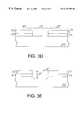
- FIG. 3Ais a cross-sectional representation of an antireflective layer supported by a semiconductor substrate.
- FIG. 3Bis a cross-sectional representation of the structure of FIG. 3A, wherein a silicon nitride layer is formed thereon.
- FIG. 3Cis a cross-sectional representation of the structure of FIG. 3B, wherein a photoresist layer is formed thereon to pattern the underlying material.
- FIG. 3Dis a cross-sectional representation of the structure of FIG. 3C, wherein the underlying stack of antireflective coating and silicon nitride layers have been patterned.
- FIG. 3Eis a cross-sectional representation of the structure of FIG. 3D, wherein field oxide is formed in field regions of the substrate between the patterned stack.
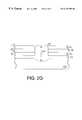
- FIGS. 4A and 4Bare cross-sectional representations of a method of trench isolation in accordance with the present invention.
- an antireflective coatingis used.
- ARCantireflective coating
- Using an ARCresults in uniform exposure to photoresist which has been formed on underlying layers of a substrate assembly.
- well-defined patternsare able to be reproduced in the photoresist.
- Forming well-defined patterns in the photoresistleads to well-defined patterning of underlying material. As device density is increasing, such precise definition is becoming increasingly important.
- substrate assemblyincludes a wide variety of semiconductor-based structures, including but not limited to a semiconductor substrate and a semiconductor substrate having one or more layers, regions formed thereon or therein.
- Semiconductor substratescan be a single layer of material, such as a silicon wafer or is understood to include silicon-on-sapphire (SOS) technology silicon-on-insulator (SOI) technology, doped and undoped semiconductors, epitaxial layers of silicon supported by a base semiconductor, as well as other semiconductor substrate structures.
- SOSsilicon-on-sapphire
- SOIsilicon-on-insulator
- ARCs according to the present inventionarc preferably inorganic. Such preferred inorganic ARCs are formed between a photoresist layer and underlying layers for use in photolithography.
- Suitable ARC materials according to the present inventioninclude a nonstoichiometric silicon-rich oxide, silicon-rich nitride, and silicon-rich oxynitride.
- a preferred chemical formula of the silicon-rich oxideis SiOX x , where x is in the range of about 0.3 to about 1.9.
- a preferred chemical formula of the silicon-rich nitrideis SiN y , where y is in the range of about 0.2 to about 1.0.
- a preferred chemical formula of the silicon-rich oxynitrideis SiO x N y , where x is in the range of about 0.2 to about 1.9 and y is in the range of about .01 to about 1.0.
- suitable ARC materialsgenerally have an index of refraction of about 1.7 to about 3.0 and an absorptive coefficient of about 0.2 to about 2.0 at a wavelength of about 248 nanometers.
- the index of refractionis about 2.0 to about 2.7 and the absorptive coefficient is about 0.4 to about 1.5 at a wavelength of about 248 nanometers.
- the absorptive coefficient neededdepends on the index of refraction and the absorptive coefficient of the photoresist and other underlying layers of the substrate assembly upon which the photoresist is formed, as well as the dimensions of the underlying substrate assembly features and layers.
- the index of refraction and the absorptive coefficient of the ARC materialtypically increase as well. For example, this is generally the case for a wavelength of about 365 nanometers.
- a layer of ARC materialis formed on a substrate assembly using chemical vapor deposition (CVD).
- CVDchemical vapor deposition
- PECVDplasma-enhanced chemical vapor deposition
- PECVDallows formation of the layer at relatively low temperatures of about 400° C.
- Silicon-rich oxideis formed by flowing a silicon-containing precursor gas and an oxygen-containing precursor gas in a process chamber.
- an inert carrier gasfor example, argon or helium
- the silicon-containing precurso gasmay be any member of the silane family (e.g., silane, disilane, dichlorosilane, etc.).
- the oxygen-containing precursor gasis nitrous oxide (N 2 O); however, other oxygen-containing precursors, including O 2 , NO, N 2 O 2 , and NO 2 , may be utilized.
- Silicon-rich nitrideis formed by flowing a silicon-containing precursor gas and a nitrogen-containing precursor gas in a process chamber.
- a carrier gasfor example, nitrogen
- the silicon-containing precursor gasmay be any member of the silane family (e.g. silane, disilane, dichlorosilane, etc.).
- the nitrogen-containing precursor gasis ammonia (NH 3 ); however, other nitrogen-containing precursor gases, such as nitrogen or a gas from the family of, [C n H 2n+1 ] 2 NH (e.g., [CH 3 ] 2 NH), may be used.
- Silicon-rich oxynitrideis formed by flowing a silicon-containing precursor gas, an oxygen-containing precursor gas, and a nitrogen-containing precursor gas in a process chamber.
- a carrier gasfor example. nitrogen
- the silicon-containing precursor gasmay, be any member of the silane family (e.g., silane, disilane, dichlorosilane, etc.).
- the oxygen-containing precursor gasis nitrous oxide (N 2 O); however, for example, O 2 , NO, N 2 O 2 , and NO 2 , may be used.
- the nitrogen-containing precursor gasis ammonia (NH 3 ); however, for example, nitrogen or a gas from the family of [C n H 3n+1 ] 2 NH, may be used.
- a layer of the ARC materialis formed in an oxidation diffusion barrier stack.
- the oxidation diffusion barrier stackis formed as a blanket layer over the supporting semiconductor structure.
- a layer of photoresistis then formed over the oxidation diffusion barrier stack.
- the photoresistis then exposed using conventional photolithography. After the photoresist is contacted with a developer solution, photoresist is selectively removed from the substrate surface according to the pattern exposed therein.
- the oxidation diffusion barrier stackis selectively etched in regions where the photoresist has been removed therefrom to pattern the stack.
- the etchantis selected according to the materials in the oxidation diffusion barrier stack.
- a dry etchis used due to the ability of dry etchants to etch anisotropically.
- the various oxide and nitride layers described hereincan be etched using any suitable etching technique.
- reactive ion etching using a fluorine chemistrymay be used to etch oxides and nitrides, e.g., a chemistry using a CHF 3 or CF 4 .
- the type of gas flowcan be easily controlled in a plasma reactor by selectively opening and closing mass controllers coupled to the plasma reactor.
- the oxidation diffusion barrier stackincludes more than one type of material, the stack can be etched in-situ due to the ability to selectively control the flow of gas.
- the exposed portions of the semiconductor substrate assemblycan be oxidized.
- the semiconductor substrate assemblye.g., doped silicon, undoped silicon
- wet oxidationis typically utilized to perform the oxidization. This process is well known to one of ordinary skill in the art. In such a process, for example, the substrate is placed in a furnace, ramped to a temperature of about 900° C. to about 1,150° C. Once the desired thickness of field oxide is grown, the temperature of the furnace is decreased and the substrate is removed from the furnace.
- the patterned oxidation diffusion barrier stackis typically removed. Once again, a dry etch, as described above, is utilized.
- the oxidation diffusion barrier stackis supported by a silicon wafer.
- a pad oxide layer 102is formed on the silicon wafer 100 .
- the silicon wafer 100is typically doped (i.e., n-type or p-type), but it is not necessary for the practice of this invention.
- the thickness 104 of the pad oxide layer 102is typically about a few hundred angstroms or less.
- an ARC layer 106is formed on the pad oxide layer 102 .
- the thickness 108 of the ARC layer 106is preferably about 100 ⁇ to about 500 ⁇ . More preferably, the thickness 108 of the ARC layer 106 is about 250 ⁇ to about 350 ⁇ . Depending on the wavelength of incident radiation during photolithograph and the dimensions of the oxidation diffusion barrier stack, however, the thickness 108 of the ARC layer 106 can vary.
- a silicon nitride layer 110is formed on the ARC layer 106 .
- the thickness 112 of the silicon nitride layer 110is preferably about 3000 ⁇ or less. More preferably, the thickness 112 of the silicon nitride layer 110 is about 1000 ⁇ to about 2400 ⁇ .
- the silicon nitride layer 110is preferable formed using low pressure chemical vapor deposition (LPCVD), for example, at a temperature of about 500° C. to about 750° C.
- LPCVDlow pressure chemical vapor deposition
- silicon nitride layeris utilized in this illustration for the purpose of an oxidation diffusion material
- any material known to prevent (or minimize) the diffusion of oxygen therethroughcan be utilized in place of, or in addition to, the silicon nitride layer 110 .
- silicon oxynitride, boron nitride, and aluminum nitridemay be used.
- a photoresist layer 114is formed on the silicon nitride layer 110 .
- the thickness 116 of the photoresist layer 114is typically about 7000 ⁇ to about 10,000 ⁇ .
- the minimum thickness 116 of the photoresist layer 114is governed by the need to have the patterned photoresist layer 114 remain after a subsequent etching step, when the oxidation diffusion barrier stack is selectively removed from the silicon wafer 100 in exposed regions underlying the patterned photoresist layer.
- the oxidation diffusion barrier stackis etched according to the technique previously described and the photoresist layer 114 is removed, resulting in the structure illustrated in FIG. 1 E.
- the photoresist layer 114is removed according to well known methods to one of ordinary skill in the art. For example, an oxygen ash can be used to remove the photoresist layer 114 .
- Regions where the oxidation diffusion barrier stack is etched to the underlying silicon wafer 100are field regions 118 .
- Regions where the patterned oxidation diffusion barrier stack remains on the silicon wafer 100are active regions 120 . Individual or multiple active devices can subsequently be formed in the active regions 120 of the substrate 100 , as is readily known to one skilled in the art.
- Field oxide 122is then formed in the field regions 118 , resulting in the structure illustrated in FIG. 1 F.
- the thickness 124 of the field oxide 122is governed by the device density and operating voltages of individual devices later formed in the active regions 120 illustrated in FIG. 1 E. Typically, the thickness 124 of the field oxide 122 is about a few thousand angstroms. The thickness 124 of the field oxide 122 , however, is not critical to the practice of this invention.
- a pad oxide layer 202is formed on the silicon wafer 200 , as illustrated in FIG. 2.
- a The silicon wafer 200is typically doped (i.e., n-type or p-type), but it is not necessary for the practice of this invention.
- the thickness 204 of the pad oxide layer 202is typically about a few hundred angstroms or less.
- a first silicon nitride layer 226is formed on the pad oxide layer 202 .
- the thickness 228 of the first silicon nitride layer 226is preferably small enough that the first silicon nitride layer 226 does not delaminate from the pad oxide layer 202 . More preferably the thickness 228 of the first silicon nitride layer 226 is about 1,500 ⁇ or less. Even more preferably, the thickness 228 of the first silicon nitride layer 226 is about 50 ⁇ to about 1,500 ⁇ . Most preferably, the thickness 228 of the first silicon nitride layer 226 is about 300 ⁇ to about 1000 ⁇ .
- the first silicon nitride layer 226can be formed using techniques well known to one of ordinary skill in the art. Preferably, one of PECVD and LPCVD is used to form the first silicon nitride layer 226 . More preferably, PECVD is used.
- an ARC layer 206is formed on the first silicon nitride layer 226 , as illustrated in FIG. 2 C.
- the thickness 208 of the ARC layer 206is about 100 ⁇ to about 500 ⁇ .
- the thickness 208 of the ARC layer 206is about 200 ⁇ to about 350 ⁇ .
- the thickness 208 of the ARC layer 206can vary.
- a second silicon nitride layer 210is formed on the ARC layer 206 .
- the thickness 212 of the second silicon nitride layer 210is preferably about 3,000 ⁇ or less. More preferably, the thickness 212 of the second silicon nitride layer 210 is selected such that a total thickness of the first and second silicon nitride layers 226 and 210 , respectively, is about 1,000 ⁇ to about 2,000 ⁇ .
- the second silicon nitride layer 110is preferably formed using low pressure chemical vapor deposition (LPCVD).
- any material known to prevent (or minimize) the diffusion of oxygen therethroughcan be utilized in place of, or in addition to, the first and second silicon nitride layers 226 and 210 .
- a photoresist layer 214is formed on the second silicon nitride layer 210 .
- the thickness 216 of the photoresist layer 214is typically about a few thousand angstroms.
- the minimum thickness 216 of the photoresist layer 214is governed by the need to prevent removal of the photoresist layer 214 through to the underlying layer during a subsequent etching step, where the oxidation diffusion barrier stack is selectively removed from the silicon wafer 200 in exposed regions underlying the photoresist layer 214 .
- the oxidation diffusion barrier stackis etched according to the technique previously described and the photoresist layer 214 is removed, resulting in the structure illustrated in FIG. 2 F.
- the photoresist layer 214is removed according to well known methods to one of ordinary skill in the art. For example, an oxygen ash can be used to remove the photoresist layer 214 .
- Regions where the oxidation diffusion barrier stack is etched to the underlying silicon wafer 200are field regions 218 .
- Regions where the patterned oxidation diffusion barrier stack remains on the silicon wafer 200are active regions 220 . Individual or multiple active devices can subsequently be formed in the active regions 220 of the substrate 200 .
- Field oxide 222is then formed in the field regions 218 , resulting in the structure illustrated in FIG. 2 G.
- the thickness 224 of the field oxide 222is governed by the device density and operating voltages of individual devices later formed in the active regions 220 illustrated in FIG. 2 F. Typically, the thickness 224 of the field oxide 222 is about a few thousand angstroms. The thickness 224 of the field oxide 222 , however, is not critical to the practice of this invention.
- an ARC layer 306is formed directly on the silicon wafer 300 as illustrated in FIG. 3 A.
- the silicon wafer 300is typically doped (i.e., n-type or p-type), but it is not necessary for the practice of this invention.
- the thickness 308 of the ARC layer 306is about 100 ⁇ to about 500 ⁇ .
- the thickness 308 of the ARC layer 306is about 200 ⁇ to about 400 ⁇ .
- the thickness 308 of the ARC layer 306can vary.
- a silicon nitride layer 310is formed on the ARC layer 306 .
- the thickness 312 of the silicon nitride layer 310is preferably about 3000 ⁇ or less. More preferably, the thickness 312 of the silicon nitride layer 310 is about 1000 ⁇ to about 2000 ⁇ .
- the silicon nitride layer 310is preferably formed using low pressure chemical vapor deposition (LPCVD). It is to be appreciated that, while a silicon nitride layer is utilized in this illustration for the purpose of an oxidation diffusion material, any material known to prevent (or minimize) the diffusion of oxygen therethrough can be utilized in place of, or in addition to, the silicon nitride layer 310 .
- a photoresist layer 314is formed on the silicon nitride layer 310 .
- the thickness 316 of the photoresist layer 314is typically about 7000 ⁇ to about 10,000 ⁇ .
- the minimum thickness 316 of the photoresist layer 314is governed by the need to prevent removal of the photoresist layer 314 through to the underlying layer during a subsequent etching step, where the oxidation diffusion barrier stack is selectively removed from the silicon wafer 300 in exposed regions underlying the photoresist layer 314 .
- the oxidation diffusion barrier stackis etched according to the technique previously described and the photoresist layer 314 is removed, resulting in the structure illustrated in FIG. 3 D.
- the photoresist layer 314is removed according to well known methods to one of ordinary skill in the art. For example, an oxygen ash can be used to remove the photoresist layer 314 .
- Regions where the oxidation diffusion barrier stack is etched to the underlying silicon wafer 300are field regions 318 .
- Regions where the patterned oxidation diffusion barrier stack remains on the silicon wafer 300are active regions 320 . Individual or multiple active devices can subsequently be formed in the active regions 320 of the substrate 300 .
- Field oxide 322is then formed in the field regions 318 , resulting in the structure illustrated in FIG. 3 E.
- the thickness 324 of the field oxide 322is governed by the device density and operating voltages of individual devices later formed in the active regions 320 illustrated in FIG. 3 D. Typically, the thickness 324 of the field oxide layer 322 is about a few thousand angstroms. The thickness 324 of the field oxide layer 322 , however, is not critical to the practice of this invention.
- this third embodimentis preferably used when process complexity is a concern. Due to the elimination of the pad oxide layer used in both the first and second embodiments and elimination of the first silicon nitride layer of the second embodiment, process efficiency is increased.
- the pad oxide layeris not necessary in this third embodiment due to the use of inorganic ARC material of the present invention. Such ARC material provides a lower stress interface with the underlying silicon substrate because it is silicon-rich. Thus, it has been found that a pad oxide layer is not necessary to relieve excess stress at the silicon interface, as is usually seen at the interface between silicon nitride and the silicon wafer.
- a trench 440is etched in the substrate assembly 442 through the oxidation diffusion barrier stack 438 .
- the trench 440is then filled with deposited oxide 444 , as illustrated in FIG. 4 B.
- Trench isolationis referred to as shallow trench isolation (STI) or deep trench isolation (DTI), depending on the thickness of the trench etched in the substrate assembly.
- the oxidation diffusion barrier stack of the present inventionis utilized in the photolithography step that defines regions in the substrate assembly to be etched for providing the trench 440 .
- the method of forming trench isolationincludes providing a semiconductor substrate assemble; forming an oxidation diffusion barrier stack having an inorganic antireflective material on the semiconductor substrate assembly; patterning the oxidation diffusion barrier stack resulting in exposed regions of the semiconductor substrate assembly; etching a trench in the semiconductor substrate assembly) as defined by the patterned stack; and depositing oxide in the trench of the semiconductor substrate assembly.
- the oxideis deposited, it is patterned so that it can be removed from areas of the substrate outside of the trench etched in the substrate.
- Conventional photolithographyis utilized to pattern the oxide.
- the oxidation diffusion barrier stack of the present inventioncan be utilized in this photolithography step. A wide variety of other uses are also suitable for use of the present invention.
Landscapes
- Engineering & Computer Science (AREA)
- Physics & Mathematics (AREA)
- General Physics & Mathematics (AREA)
- Condensed Matter Physics & Semiconductors (AREA)
- Manufacturing & Machinery (AREA)
- Computer Hardware Design (AREA)
- Microelectronics & Electronic Packaging (AREA)
- Power Engineering (AREA)
- Architecture (AREA)
- Structural Engineering (AREA)
- Chemical & Material Sciences (AREA)
- Inorganic Chemistry (AREA)
- Element Separation (AREA)
- Formation Of Insulating Films (AREA)
- Local Oxidation Of Silicon (AREA)
- Internal Circuitry In Semiconductor Integrated Circuit Devices (AREA)
- Exposure Of Semiconductors, Excluding Electron Or Ion Beam Exposure (AREA)
Abstract
Description
Claims (18)
Priority Applications (1)
| Application Number | Priority Date | Filing Date | Title |
|---|---|---|---|
| US09/179,722US6174590B1 (en) | 1997-08-22 | 1998-10-14 | Isolation using an antireflective coating |
Applications Claiming Priority (2)
| Application Number | Priority Date | Filing Date | Title |
|---|---|---|---|
| US08/916,276US6121133A (en) | 1997-08-22 | 1997-08-22 | Isolation using an antireflective coating |
| US09/179,722US6174590B1 (en) | 1997-08-22 | 1998-10-14 | Isolation using an antireflective coating |
Related Parent Applications (1)
| Application Number | Title | Priority Date | Filing Date |
|---|---|---|---|
| US08/916,276DivisionUS6121133A (en) | 1997-08-22 | 1997-08-22 | Isolation using an antireflective coating |
Publications (1)
| Publication Number | Publication Date |
|---|---|
| US6174590B1true US6174590B1 (en) | 2001-01-16 |
Family
ID=25436986
Family Applications (5)
| Application Number | Title | Priority Date | Filing Date |
|---|---|---|---|
| US08/916,276Expired - LifetimeUS6121133A (en) | 1997-08-22 | 1997-08-22 | Isolation using an antireflective coating |
| US09/179,722Expired - LifetimeUS6174590B1 (en) | 1997-08-22 | 1998-10-14 | Isolation using an antireflective coating |
| US09/620,790Expired - LifetimeUS6495450B1 (en) | 1997-08-22 | 2000-07-21 | Isolation using an antireflective coating |
| US09/625,164Expired - LifetimeUS6423631B1 (en) | 1997-08-22 | 2000-07-25 | Isolation using an antireflective coating |
| US10/172,895Expired - LifetimeUS6605502B2 (en) | 1997-08-22 | 2002-06-17 | Isolation using an antireflective coating |
Family Applications Before (1)
| Application Number | Title | Priority Date | Filing Date |
|---|---|---|---|
| US08/916,276Expired - LifetimeUS6121133A (en) | 1997-08-22 | 1997-08-22 | Isolation using an antireflective coating |
Family Applications After (3)
| Application Number | Title | Priority Date | Filing Date |
|---|---|---|---|
| US09/620,790Expired - LifetimeUS6495450B1 (en) | 1997-08-22 | 2000-07-21 | Isolation using an antireflective coating |
| US09/625,164Expired - LifetimeUS6423631B1 (en) | 1997-08-22 | 2000-07-25 | Isolation using an antireflective coating |
| US10/172,895Expired - LifetimeUS6605502B2 (en) | 1997-08-22 | 2002-06-17 | Isolation using an antireflective coating |
Country Status (6)
| Country | Link |
|---|---|
| US (5) | US6121133A (en) |
| EP (1) | EP1019951A1 (en) |
| JP (1) | JP3978310B2 (en) |
| KR (1) | KR100424533B1 (en) |
| AU (1) | AU9109798A (en) |
| WO (1) | WO1999010918A1 (en) |
Cited By (13)
| Publication number | Priority date | Publication date | Assignee | Title |
|---|---|---|---|---|
| US6268299B1 (en)* | 2000-09-25 | 2001-07-31 | International Business Machines Corporation | Variable stoichiometry silicon nitride barrier films for tunable etch selectivity and enhanced hyrogen permeability |
| US6423631B1 (en) | 1997-08-22 | 2002-07-23 | Micron Technology, Inc. | Isolation using an antireflective coating |
| US6444588B1 (en) | 1999-04-26 | 2002-09-03 | Micron Technology, Inc. | Anti-reflective coatings and methods regarding same |
| US6541843B2 (en) | 1998-09-03 | 2003-04-01 | Micron Technology, Inc. | Anti-reflective coatings and methods for forming and using same |
| US6569784B1 (en) | 2001-07-20 | 2003-05-27 | Taiwan Semiconductor Manufacturing Company | Material of photoresist protect oxide |
| DE10156865A1 (en)* | 2001-11-20 | 2003-05-28 | Infineon Technologies Ag | Process for forming a structure in a semiconductor substrate comprises transferring a photolithographic structure on a photoresist layer into an anti-reflective layer |
| US6573175B1 (en) | 2001-11-30 | 2003-06-03 | Micron Technology, Inc. | Dry low k film application for interlevel dielectric and method of cleaning etched features |
| US6841491B1 (en)* | 2001-11-08 | 2005-01-11 | Cypress Semiconductor Corporation | In situ deposition of a nitride layer and of an anti-reflective layer |
| US6858898B1 (en)* | 1999-03-23 | 2005-02-22 | Semiconductor Energy Laboratory Co., Ltd. | Semiconductor device and method for manufacturing the same |
| US6940124B2 (en) | 1999-04-30 | 2005-09-06 | Semiconductor Energy Laboratory Co., Ltd. | Semiconductor device and manufacturing method thereof |
| US20060003500A1 (en)* | 1997-11-10 | 2006-01-05 | Chia-Gee Wang | Epitaxial siox barrier/insulation layer |
| US7915175B1 (en) | 2004-06-25 | 2011-03-29 | Cypress Semiconductor Corporation | Etching nitride and anti-reflective coating |
| US20110151222A1 (en)* | 2009-12-22 | 2011-06-23 | Agc Flat Glass North America, Inc. | Anti-reflective coatings and methods of making the same |
Families Citing this family (43)
| Publication number | Priority date | Publication date | Assignee | Title |
|---|---|---|---|---|
| US6436746B1 (en)* | 1998-01-12 | 2002-08-20 | Texas Instruments Incorporated | Transistor having an improved gate structure and method of construction |
| US6274292B1 (en) | 1998-02-25 | 2001-08-14 | Micron Technology, Inc. | Semiconductor processing methods |
| US7804115B2 (en) | 1998-02-25 | 2010-09-28 | Micron Technology, Inc. | Semiconductor constructions having antireflective portions |
| DE69835276T2 (en)* | 1998-05-22 | 2007-07-12 | Applied Materials, Inc., Santa Clara | A method of making a self-planarized dielectric layer for shallow trench isolation |
| US6268282B1 (en)* | 1998-09-03 | 2001-07-31 | Micron Technology, Inc. | Semiconductor processing methods of forming and utilizing antireflective material layers, and methods of forming transistor gate stacks |
| US6281100B1 (en) | 1998-09-03 | 2001-08-28 | Micron Technology, Inc. | Semiconductor processing methods |
| US6828683B2 (en) | 1998-12-23 | 2004-12-07 | Micron Technology, Inc. | Semiconductor devices, and semiconductor processing methods |
| US6291361B1 (en)* | 1999-03-24 | 2001-09-18 | Conexant Systems, Inc. | Method and apparatus for high-resolution in-situ plasma etching of inorganic and metal films |
| US6335235B1 (en)* | 1999-08-17 | 2002-01-01 | Advanced Micro Devices, Inc. | Simplified method of patterning field dielectric regions in a semiconductor device |
| US7067414B1 (en) | 1999-09-01 | 2006-06-27 | Micron Technology, Inc. | Low k interlevel dielectric layer fabrication methods |
| US6440860B1 (en) | 2000-01-18 | 2002-08-27 | Micron Technology, Inc. | Semiconductor processing methods of transferring patterns from patterned photoresists to materials, and structures comprising silicon nitride |
| JP2001313389A (en)* | 2000-05-01 | 2001-11-09 | Seiko Epson Corp | Semiconductor device and method of manufacturing the same |
| US6607984B1 (en)* | 2000-06-20 | 2003-08-19 | International Business Machines Corporation | Removable inorganic anti-reflection coating process |
| US7172960B2 (en)* | 2000-12-27 | 2007-02-06 | Intel Corporation | Multi-layer film stack for extinction of substrate reflections during patterning |
| US20020197835A1 (en)* | 2001-06-06 | 2002-12-26 | Sey-Ping Sun | Anti-reflective coating and methods of making the same |
| US6613649B2 (en)* | 2001-12-05 | 2003-09-02 | Chartered Semiconductor Manufacturing Ltd | Method for buffer STI scheme with a hard mask layer as an oxidation barrier |
| US6713404B2 (en)* | 2002-03-05 | 2004-03-30 | Micron Technology, Inc. | Methods of forming semiconductor constructions |
| DE10218955B4 (en) | 2002-04-27 | 2004-09-09 | Infineon Technologies Ag | Method for producing a structured layer on a semiconductor substrate |
| US6743726B2 (en)* | 2002-07-11 | 2004-06-01 | Promos Technologies, Inc. | Method for etching a trench through an anti-reflective coating |
| DE10250902B4 (en)* | 2002-10-31 | 2009-06-18 | Advanced Micro Devices, Inc., Sunnyvale | A method of removing structural elements using an improved ablation process in the manufacture of a semiconductor device |
| US7510927B2 (en)* | 2002-12-26 | 2009-03-31 | Intel Corporation | LOCOS isolation for fully-depleted SOI devices |
| US6946352B2 (en)* | 2003-07-24 | 2005-09-20 | Taiwan Semiconductor Manufacturing Company, Ltd. | CMOS image sensor device and method |
| US7300702B2 (en)* | 2003-08-18 | 2007-11-27 | Honeywell International, Inc. | Diffusion barrier coating for Si-based components |
| US6979627B2 (en)* | 2004-04-30 | 2005-12-27 | Freescale Semiconductor, Inc. | Isolation trench |
| US20060071301A1 (en)* | 2004-10-06 | 2006-04-06 | Luo Shing A | Silicon rich dielectric antireflective coating |
| US7651955B2 (en)* | 2005-06-21 | 2010-01-26 | Applied Materials, Inc. | Method for forming silicon-containing materials during a photoexcitation deposition process |
| JP4499623B2 (en)* | 2005-06-28 | 2010-07-07 | Okiセミコンダクタ株式会社 | Manufacturing method of semiconductor device |
| JP5069109B2 (en)* | 2005-06-29 | 2012-11-07 | スパンション エルエルシー | Semiconductor device and manufacturing method thereof |
| US7276417B2 (en)* | 2005-12-28 | 2007-10-02 | Taiwan Semiconductor Manufacturing Company, Ltd. | Hybrid STI stressor with selective re-oxidation anneal |
| US20070236798A1 (en)* | 2006-04-05 | 2007-10-11 | Shelestak Larry J | Antireflective coating and substrates coated therewith |
| US7670895B2 (en) | 2006-04-24 | 2010-03-02 | Freescale Semiconductor, Inc | Process of forming an electronic device including a semiconductor layer and another layer adjacent to an opening within the semiconductor layer |
| US20070249127A1 (en)* | 2006-04-24 | 2007-10-25 | Freescale Semiconductor, Inc. | Electronic device including a semiconductor layer and a sidewall spacer and a process of forming the same |
| US7491622B2 (en)* | 2006-04-24 | 2009-02-17 | Freescale Semiconductor, Inc. | Process of forming an electronic device including a layer formed using an inductively coupled plasma |
| US7528078B2 (en) | 2006-05-12 | 2009-05-05 | Freescale Semiconductor, Inc. | Process of forming electronic device including a densified nitride layer adjacent to an opening within a semiconductor layer |
| DE102006048960B4 (en)* | 2006-10-17 | 2016-12-15 | Texas Instruments Deutschland Gmbh | Method for producing insulation structures with integrated deep and shallow trenches |
| US7951707B2 (en)* | 2007-03-21 | 2011-05-31 | Macronix International Co., Ltd. | Etching method for semiconductor element |
| JP2010527146A (en)* | 2007-05-07 | 2010-08-05 | ジョージア テック リサーチ コーポレイション | Formation of high quality back contact with screen printed local back surface field |
| US7772094B2 (en) | 2007-12-28 | 2010-08-10 | Texas Instuments Incorporated | Implant damage of layer for easy removal and reduced silicon recess |
| US20090286349A1 (en)* | 2008-05-13 | 2009-11-19 | Georgia Tech Research Corporation | Solar cell spin-on based process for simultaneous diffusion and passivation |
| JP5332776B2 (en)* | 2009-03-18 | 2013-11-06 | 凸版印刷株式会社 | Method for manufacturing transfer mask |
| US8980711B2 (en)* | 2012-02-28 | 2015-03-17 | Taiwan Semiconductor Manufacturing Company, Ltd. | Memory device structure and method |
| US10566200B2 (en)* | 2018-04-03 | 2020-02-18 | Texas Instruments Incorporated | Method of fabricating transistors, including ambient oxidizing after etchings into barrier layers and anti-reflecting coatings |
| US20200286742A1 (en)* | 2019-03-06 | 2020-09-10 | Kateeva, Inc. | Remote plasma etch using inkjet printed etch mask |
Citations (13)
| Publication number | Priority date | Publication date | Assignee | Title |
|---|---|---|---|---|
| JPS6159820A (en) | 1984-08-31 | 1986-03-27 | Fujitsu Ltd | Manufacturing method of semiconductor device |
| US4764248A (en) | 1987-04-13 | 1988-08-16 | Cypress Semiconductor Corporation | Rapid thermal nitridized oxide locos process |
| JPH03101147A (en) | 1989-09-13 | 1991-04-25 | Toshiba Corp | Manufacture of semiconductor device |
| US5216542A (en) | 1989-12-19 | 1993-06-01 | Leybold Aktiengesellschaft | Coating, composed of an optically effective layer system, for substrates, whereby the layer system has a high anti-reflective effect, and method for the manufacturing of the coating |
| US5374585A (en) | 1994-05-09 | 1994-12-20 | Motorola, Inc. | Process for forming field isolation |
| US5418019A (en) | 1994-05-25 | 1995-05-23 | Georgia Tech Research Corporation | Method for low temperature plasma enhanced chemical vapor deposition (PECVD) of an oxide and nitride antireflection coating on silicon |
| US5441914A (en) | 1994-05-02 | 1995-08-15 | Motorola Inc. | Method of forming conductive interconnect structure |
| JPH0831811A (en) | 1994-07-15 | 1996-02-02 | Sony Corp | Method for forming element isolation area of semiconductor device |
| JPH0831812A (en) | 1994-07-15 | 1996-02-02 | Sony Corp | Formation of element-isolating area for semiconductor device |
| US5510271A (en) | 1994-09-09 | 1996-04-23 | Georgia Tech Research Corporation | Processes for producing low cost, high efficiency silicon solar cells |
| US5539249A (en) | 1993-07-06 | 1996-07-23 | Motorola, Inc. | Method and structure for forming an integrated circuit pattern on a semiconductor substrate |
| US5580815A (en) | 1993-08-12 | 1996-12-03 | Motorola Inc. | Process for forming field isolation and a structure over a semiconductor substrate |
| JPH09134914A (en) | 1995-11-08 | 1997-05-20 | Oki Electric Ind Co Ltd | Formation of element isolation region |
Family Cites Families (31)
| Publication number | Priority date | Publication date | Assignee | Title |
|---|---|---|---|---|
| JPS5642377A (en) | 1979-09-14 | 1981-04-20 | Fujitsu Ltd | Ultraviolet ray erasable type rewritable read-only memory |
| JPS5690525A (en) | 1979-11-28 | 1981-07-22 | Fujitsu Ltd | Manufacture of semiconductor device |
| JPS5693344A (en) | 1979-12-26 | 1981-07-28 | Fujitsu Ltd | Manufacture of semiconductor device |
| US4451969A (en) | 1983-01-10 | 1984-06-05 | Mobil Solar Energy Corporation | Method of fabricating solar cells |
| JPH0752673B2 (en)* | 1989-01-18 | 1995-06-05 | シャープ株式会社 | Thin film EL device |
| US4921572A (en) | 1989-05-04 | 1990-05-01 | Olin Corporation | Etchant solutions containing hydrogen fluoride and a polyammonium fluoride salt |
| US5677111A (en) | 1991-12-20 | 1997-10-14 | Sony Corporation | Process for production of micropattern utilizing antireflection film |
| US5472827A (en) | 1991-12-30 | 1995-12-05 | Sony Corporation | Method of forming a resist pattern using an anti-reflective layer |
| US5270241A (en) | 1992-03-13 | 1993-12-14 | Micron Technology, Inc. | Optimized container stacked capacitor DRAM cell utilizing sacrificial oxide deposition and chemical mechanical polishing |
| DE4231312C2 (en)* | 1992-09-18 | 1996-10-02 | Siemens Ag | Anti-reflective layer and method for the lithographic structuring of a layer |
| US5392189A (en) | 1993-04-02 | 1995-02-21 | Micron Semiconductor, Inc. | Capacitor compatible with high dielectric constant materials having two independent insulative layers and the method for forming same |
| JP3101147B2 (en) | 1994-05-02 | 2000-10-23 | シャープ株式会社 | Copier |
| US5710067A (en) | 1995-06-07 | 1998-01-20 | Advanced Micro Devices, Inc. | Silicon oxime film |
| US5716535A (en) | 1996-03-05 | 1998-02-10 | Micron Technology, Inc. | Methods and etchants for etching oxides of silicon with low selectivity |
| US6127262A (en) | 1996-06-28 | 2000-10-03 | Applied Materials, Inc. | Method and apparatus for depositing an etch stop layer |
| US5994217A (en) | 1996-12-16 | 1999-11-30 | Chartered Semiconductor Manufacturing Ltd. | Post metallization stress relief annealing heat treatment for ARC TiN over aluminum layers |
| US5796151A (en)* | 1996-12-19 | 1998-08-18 | Texas Instruments Incorporated | Semiconductor stack having a dielectric sidewall for prevention of oxidation of tungsten in tungsten capped poly-silicon gate electrodes |
| US5886391A (en) | 1997-04-18 | 1999-03-23 | Micron Technology, Inc. | Antireflective structure |
| US5930627A (en) | 1997-05-05 | 1999-07-27 | Chartered Semiconductor Manufacturing Company, Ltd. | Process improvements in self-aligned polysilicon MOSFET technology using silicon oxynitride |
| US6121133A (en) | 1997-08-22 | 2000-09-19 | Micron Technology, Inc. | Isolation using an antireflective coating |
| US6114235A (en) | 1997-09-05 | 2000-09-05 | Advanced Micro Devices, Inc. | Multipurpose cap layer dielectric |
| US5990524A (en) | 1997-12-18 | 1999-11-23 | Advanced Micro Devices, Inc. | Silicon oxime spacer for preventing over-etching during local interconnect formation |
| US6117741A (en) | 1998-01-09 | 2000-09-12 | Texas Instruments Incorporated | Method of forming a transistor having an improved sidewall gate structure |
| US6274292B1 (en) | 1998-02-25 | 2001-08-14 | Micron Technology, Inc. | Semiconductor processing methods |
| US6103456A (en) | 1998-07-22 | 2000-08-15 | Siemens Aktiengesellschaft | Prevention of photoresist poisoning from dielectric antireflective coating in semiconductor fabrication |
| US6294459B1 (en) | 1998-09-03 | 2001-09-25 | Micron Technology, Inc. | Anti-reflective coatings and methods for forming and using same |
| US6380611B1 (en) | 1998-09-03 | 2002-04-30 | Micron Technology, Inc. | Treatment for film surface to reduce photo footing |
| US6228760B1 (en) | 1999-03-08 | 2001-05-08 | Taiwan Semiconductor Manufacturing Company | Use of PE-SiON or PE-OXIDE for contact or via photo and for defect reduction with oxide and W chemical-mechanical polish |
| US6444588B1 (en) | 1999-04-26 | 2002-09-03 | Micron Technology, Inc. | Anti-reflective coatings and methods regarding same |
| US6124178A (en) | 1999-08-26 | 2000-09-26 | Mosel Vitelic, Inc. | Method of manufacturing MOSFET devices |
| US6225216B1 (en) | 1999-10-15 | 2001-05-01 | Advanced Micro Devices, Inc. | Method of forming a local interconnect with improved etch selectivity of silicon dioxide/silicide |
- 1997
- 1997-08-22USUS08/916,276patent/US6121133A/ennot_activeExpired - Lifetime
- 1998
- 1998-08-20AUAU91097/98Apatent/AU9109798A/ennot_activeAbandoned
- 1998-08-20KRKR10-2000-7001831Apatent/KR100424533B1/ennot_activeExpired - Fee Related
- 1998-08-20EPEP98943267Apatent/EP1019951A1/ennot_activeWithdrawn
- 1998-08-20JPJP2000508135Apatent/JP3978310B2/ennot_activeExpired - Fee Related
- 1998-08-20WOPCT/US1998/017267patent/WO1999010918A1/enactiveIP Right Grant
- 1998-10-14USUS09/179,722patent/US6174590B1/ennot_activeExpired - Lifetime
- 2000
- 2000-07-21USUS09/620,790patent/US6495450B1/ennot_activeExpired - Lifetime
- 2000-07-25USUS09/625,164patent/US6423631B1/ennot_activeExpired - Lifetime
- 2002
- 2002-06-17USUS10/172,895patent/US6605502B2/ennot_activeExpired - Lifetime
Patent Citations (14)
| Publication number | Priority date | Publication date | Assignee | Title |
|---|---|---|---|---|
| JPS6159820A (en) | 1984-08-31 | 1986-03-27 | Fujitsu Ltd | Manufacturing method of semiconductor device |
| US4764248A (en) | 1987-04-13 | 1988-08-16 | Cypress Semiconductor Corporation | Rapid thermal nitridized oxide locos process |
| JPH03101147A (en) | 1989-09-13 | 1991-04-25 | Toshiba Corp | Manufacture of semiconductor device |
| US5216542A (en) | 1989-12-19 | 1993-06-01 | Leybold Aktiengesellschaft | Coating, composed of an optically effective layer system, for substrates, whereby the layer system has a high anti-reflective effect, and method for the manufacturing of the coating |
| US5539249A (en) | 1993-07-06 | 1996-07-23 | Motorola, Inc. | Method and structure for forming an integrated circuit pattern on a semiconductor substrate |
| US5639687A (en) | 1993-07-06 | 1997-06-17 | Motorola Inc. | Method for forming an integrated circuit pattern on a semiconductor substrate using silicon-rich silicon nitride |
| US5580815A (en) | 1993-08-12 | 1996-12-03 | Motorola Inc. | Process for forming field isolation and a structure over a semiconductor substrate |
| US5441914A (en) | 1994-05-02 | 1995-08-15 | Motorola Inc. | Method of forming conductive interconnect structure |
| US5374585A (en) | 1994-05-09 | 1994-12-20 | Motorola, Inc. | Process for forming field isolation |
| US5418019A (en) | 1994-05-25 | 1995-05-23 | Georgia Tech Research Corporation | Method for low temperature plasma enhanced chemical vapor deposition (PECVD) of an oxide and nitride antireflection coating on silicon |
| JPH0831812A (en) | 1994-07-15 | 1996-02-02 | Sony Corp | Formation of element-isolating area for semiconductor device |
| JPH0831811A (en) | 1994-07-15 | 1996-02-02 | Sony Corp | Method for forming element isolation area of semiconductor device |
| US5510271A (en) | 1994-09-09 | 1996-04-23 | Georgia Tech Research Corporation | Processes for producing low cost, high efficiency silicon solar cells |
| JPH09134914A (en) | 1995-11-08 | 1997-05-20 | Oki Electric Ind Co Ltd | Formation of element isolation region |
Non-Patent Citations (5)
| Title |
|---|
| C. Bencher et al., "Dielectric antireflective coatings for DUV lithography", Solid State Technology, pp. 109, 111-112, and 114 (1997). |
| T. Gocho et al., "CVD Method of Anti-Reflective Layer Film for Excimer Laser Lithography", Int. Conf. On Solid State Devices & Materials, Makuhari, Aug. 29-Sep. 1, pp. 570-572 (1993). |
| T.P. Ong et al., "CVD SiNx Anti-reflective Coating for Sub-0.5 mum Lithography", Symposium on VLSI Technology Digest of Technical Papers, pp. 73-74 (1995). |
| T.P. Ong et al., "CVD SiNx Anti-reflective Coating for Sub-0.5 μm Lithography", Symposium on VLSI Technology Digest of Technical Papers, pp. 73-74 (1995). |
| Wolf, S., "Silicon Processing for the VLSI Era", The Submicron Mosfet, 3, 339-341 (1995). |
Cited By (37)
| Publication number | Priority date | Publication date | Assignee | Title |
|---|---|---|---|---|
| US6423631B1 (en) | 1997-08-22 | 2002-07-23 | Micron Technology, Inc. | Isolation using an antireflective coating |
| US6495450B1 (en) | 1997-08-22 | 2002-12-17 | Micron Technology, Inc. | Isolation using an antireflective coating |
| US6605502B2 (en) | 1997-08-22 | 2003-08-12 | Micron Technology, Inc. | Isolation using an antireflective coating |
| US7105895B2 (en)* | 1997-11-10 | 2006-09-12 | Nanodynamics, Inc. | Epitaxial SiOx barrier/insulation layer |
| US20060003500A1 (en)* | 1997-11-10 | 2006-01-05 | Chia-Gee Wang | Epitaxial siox barrier/insulation layer |
| US6673713B2 (en) | 1998-09-03 | 2004-01-06 | Micron Technology, Inc. | Anti-reflective coatings and methods for forming and using same |
| US6541843B2 (en) | 1998-09-03 | 2003-04-01 | Micron Technology, Inc. | Anti-reflective coatings and methods for forming and using same |
| US6784094B2 (en) | 1998-09-03 | 2004-08-31 | Micron Technology, Inc. | Anti-reflective coatings and methods for forming and using same |
| US20040137718A1 (en)* | 1998-09-03 | 2004-07-15 | Micron Technology, Inc. | Anti-reflective coatings and methods for forming and using same |
| US9806096B2 (en) | 1999-03-23 | 2017-10-31 | Semiconductor Energy Laboratory Co., Ltd. | Semiconductor device and method for manufacturing the same |
| US7064388B2 (en) | 1999-03-23 | 2006-06-20 | Semiconductor Energy Laboratory Co., Ltd. | Semiconductor device and method for manufacturing the same |
| US8610182B2 (en) | 1999-03-23 | 2013-12-17 | Semiconductor Energy Laboratory Co., Ltd. | Semiconductor device and method for manufacturing the same |
| US7821071B2 (en) | 1999-03-23 | 2010-10-26 | Semiconductor Energy Laboratory Co., Ltd. | Semiconductor device and method for manufacturing the same |
| US20090224260A1 (en)* | 1999-03-23 | 2009-09-10 | Semiconductor Energy Laboratory Co., Ltd. | Semiconductor Device and Method for Manufacturing the Same |
| US7504343B2 (en) | 1999-03-23 | 2009-03-17 | Semiconductor Energy Laboratory Co., Ltd. | Semiconductor device and method for manufacturing the same |
| US8154059B2 (en) | 1999-03-23 | 2012-04-10 | Semiconductor Energy Laboratory Co., Ltd. | Semiconductor device and method for manufacturing the same |
| US20060267114A1 (en)* | 1999-03-23 | 2006-11-30 | Semiconductor Energy Laboratory Co., Ltd. | Semiconductor device and method for manufacturing the same |
| US6858898B1 (en)* | 1999-03-23 | 2005-02-22 | Semiconductor Energy Laboratory Co., Ltd. | Semiconductor device and method for manufacturing the same |
| US20110034215A1 (en)* | 1999-03-23 | 2011-02-10 | Semiconductor Energy Laboratory Co., Ltd. | Semiconductor Device and Method for Manufacturing the Same |
| US9196632B2 (en) | 1999-03-23 | 2015-11-24 | Semiconductor Energy Laboratory Co., Ltd. | Semiconductor device and method for manufacturing the same |
| US6444588B1 (en) | 1999-04-26 | 2002-09-03 | Micron Technology, Inc. | Anti-reflective coatings and methods regarding same |
| US6940124B2 (en) | 1999-04-30 | 2005-09-06 | Semiconductor Energy Laboratory Co., Ltd. | Semiconductor device and manufacturing method thereof |
| US7456474B2 (en) | 1999-04-30 | 2008-11-25 | Semiconductor Energy Laboratory Co., Ltd. | Semiconductor device having insulating film |
| US7855416B2 (en) | 1999-04-30 | 2010-12-21 | Semiconductor Energy Laboratory Co., Ltd. | Semiconductor device and manufacturing method thereof |
| US20090224255A1 (en)* | 1999-04-30 | 2009-09-10 | Semiconductor Energy Laboratory Co., Ltd. | Semiconductor Device and Manufacturing Method Thereof |
| US6268299B1 (en)* | 2000-09-25 | 2001-07-31 | International Business Machines Corporation | Variable stoichiometry silicon nitride barrier films for tunable etch selectivity and enhanced hyrogen permeability |
| US6569784B1 (en) | 2001-07-20 | 2003-05-27 | Taiwan Semiconductor Manufacturing Company | Material of photoresist protect oxide |
| US6841491B1 (en)* | 2001-11-08 | 2005-01-11 | Cypress Semiconductor Corporation | In situ deposition of a nitride layer and of an anti-reflective layer |
| DE10156865A1 (en)* | 2001-11-20 | 2003-05-28 | Infineon Technologies Ag | Process for forming a structure in a semiconductor substrate comprises transferring a photolithographic structure on a photoresist layer into an anti-reflective layer |
| US6605863B2 (en) | 2001-11-30 | 2003-08-12 | Micron Technology, Inc. | Low k film application for interlevel dielectric and method of cleaning etched features |
| US6890865B2 (en) | 2001-11-30 | 2005-05-10 | Micron Technology, Inc. | Low k film application for interlevel dielectric and method of cleaning etched features |
| US20040245644A1 (en)* | 2001-11-30 | 2004-12-09 | Micron Technology, Inc. | Low K film application for interlevel dielectric and method of cleaning etched features |
| US20030205785A1 (en)* | 2001-11-30 | 2003-11-06 | Micron Technology, Inc. | Low k film application for interlevel dielectric and method of cleaning etched features |
| US20030207514A1 (en)* | 2001-11-30 | 2003-11-06 | Micron Technology, Inc. | Low k film application for interlevel dielectric and method of cleaning etched features |
| US6573175B1 (en) | 2001-11-30 | 2003-06-03 | Micron Technology, Inc. | Dry low k film application for interlevel dielectric and method of cleaning etched features |
| US7915175B1 (en) | 2004-06-25 | 2011-03-29 | Cypress Semiconductor Corporation | Etching nitride and anti-reflective coating |
| US20110151222A1 (en)* | 2009-12-22 | 2011-06-23 | Agc Flat Glass North America, Inc. | Anti-reflective coatings and methods of making the same |
Also Published As
| Publication number | Publication date |
|---|---|
| AU9109798A (en) | 1999-03-16 |
| US6605502B2 (en) | 2003-08-12 |
| WO1999010918A1 (en) | 1999-03-04 |
| KR20010023202A (en) | 2001-03-26 |
| EP1019951A1 (en) | 2000-07-19 |
| US6495450B1 (en) | 2002-12-17 |
| KR100424533B1 (en) | 2004-03-27 |
| US6121133A (en) | 2000-09-19 |
| US6423631B1 (en) | 2002-07-23 |
| US20020155698A1 (en) | 2002-10-24 |
| JP2001514445A (en) | 2001-09-11 |
| JP3978310B2 (en) | 2007-09-19 |
Similar Documents
| Publication | Publication Date | Title |
|---|---|---|
| US6174590B1 (en) | Isolation using an antireflective coating | |
| US7125783B2 (en) | Dielectric anti-reflective coating surface treatment to prevent defect generation in associated wet clean | |
| KR100870616B1 (en) | Methods of Forming Trench Isolation Regions | |
| US6764922B2 (en) | Method of formation of an oxynitride shallow trench isolation | |
| US5786262A (en) | Self-planarized gapfilling for shallow trench isolation | |
| US6287962B1 (en) | Method for making a novel graded silicon nitride/silicon oxide (SNO) hard mask for improved deep sub-micrometer semiconductor processing | |
| US5445989A (en) | Method of forming device isolation regions | |
| US5930646A (en) | Method of shallow trench isolation | |
| US6444588B1 (en) | Anti-reflective coatings and methods regarding same | |
| US5643833A (en) | Method of making a contact hole in a semiconductor device | |
| US6255717B1 (en) | Shallow trench isolation using antireflection layer | |
| US6001704A (en) | Method of fabricating a shallow trench isolation by using oxide/oxynitride layers | |
| US6509271B1 (en) | Manufacturing method of semiconductor device | |
| US6083808A (en) | Method for forming a trench isolation in a semiconductor device | |
| US5786229A (en) | Method for providing isolation between semiconductor devices using epitaxial growth and polishing | |
| US6194288B1 (en) | Implant N2 into a pad oxide film to mask the active region and grow field oxide without Si3N4 film | |
| KR100318461B1 (en) | Semiconductor device isolation method | |
| US6821883B1 (en) | Shallow trench isolation using antireflection layer | |
| JPH07302791A (en) | Formation of field oxidized film of semiconductor element | |
| US7061075B1 (en) | Shallow trench isolation using antireflection layer | |
| US7842451B2 (en) | Method of forming pattern | |
| KR100292387B1 (en) | Trench manufacturing method for semiconductor device isolation | |
| KR100361520B1 (en) | A method of device isolation in semiconductor device | |
| KR100315029B1 (en) | Trench Formation Method of Semiconductor Device | |
| KR20030081897A (en) | Method of fabricating a semiconductor device with a silicon nitride having a high extinction coefficient |
Legal Events
| Date | Code | Title | Description |
|---|---|---|---|
| FEPP | Fee payment procedure | Free format text:PAYOR NUMBER ASSIGNED (ORIGINAL EVENT CODE: ASPN); ENTITY STATUS OF PATENT OWNER: LARGE ENTITY | |
| STCF | Information on status: patent grant | Free format text:PATENTED CASE | |
| CC | Certificate of correction | ||
| FPAY | Fee payment | Year of fee payment:4 | |
| FPAY | Fee payment | Year of fee payment:8 | |
| FPAY | Fee payment | Year of fee payment:12 | |
| AS | Assignment | Owner name:U.S. BANK NATIONAL ASSOCIATION, AS COLLATERAL AGENT, CALIFORNIA Free format text:SECURITY INTEREST;ASSIGNOR:MICRON TECHNOLOGY, INC.;REEL/FRAME:038669/0001 Effective date:20160426 Owner name:U.S. BANK NATIONAL ASSOCIATION, AS COLLATERAL AGEN Free format text:SECURITY INTEREST;ASSIGNOR:MICRON TECHNOLOGY, INC.;REEL/FRAME:038669/0001 Effective date:20160426 | |
| AS | Assignment | Owner name:MORGAN STANLEY SENIOR FUNDING, INC., AS COLLATERAL AGENT, MARYLAND Free format text:PATENT SECURITY AGREEMENT;ASSIGNOR:MICRON TECHNOLOGY, INC.;REEL/FRAME:038954/0001 Effective date:20160426 Owner name:MORGAN STANLEY SENIOR FUNDING, INC., AS COLLATERAL Free format text:PATENT SECURITY AGREEMENT;ASSIGNOR:MICRON TECHNOLOGY, INC.;REEL/FRAME:038954/0001 Effective date:20160426 | |
| AS | Assignment | Owner name:U.S. BANK NATIONAL ASSOCIATION, AS COLLATERAL AGENT, CALIFORNIA Free format text:CORRECTIVE ASSIGNMENT TO CORRECT THE REPLACE ERRONEOUSLY FILED PATENT #7358718 WITH THE CORRECT PATENT #7358178 PREVIOUSLY RECORDED ON REEL 038669 FRAME 0001. ASSIGNOR(S) HEREBY CONFIRMS THE SECURITY INTEREST;ASSIGNOR:MICRON TECHNOLOGY, INC.;REEL/FRAME:043079/0001 Effective date:20160426 Owner name:U.S. BANK NATIONAL ASSOCIATION, AS COLLATERAL AGEN Free format text:CORRECTIVE ASSIGNMENT TO CORRECT THE REPLACE ERRONEOUSLY FILED PATENT #7358718 WITH THE CORRECT PATENT #7358178 PREVIOUSLY RECORDED ON REEL 038669 FRAME 0001. ASSIGNOR(S) HEREBY CONFIRMS THE SECURITY INTEREST;ASSIGNOR:MICRON TECHNOLOGY, INC.;REEL/FRAME:043079/0001 Effective date:20160426 | |
| AS | Assignment | Owner name:MICRON TECHNOLOGY, INC., IDAHO Free format text:RELEASE BY SECURED PARTY;ASSIGNOR:U.S. BANK NATIONAL ASSOCIATION, AS COLLATERAL AGENT;REEL/FRAME:047243/0001 Effective date:20180629 | |
| AS | Assignment | Owner name:MICRON TECHNOLOGY, INC., IDAHO Free format text:RELEASE BY SECURED PARTY;ASSIGNOR:MORGAN STANLEY SENIOR FUNDING, INC., AS COLLATERAL AGENT;REEL/FRAME:050937/0001 Effective date:20190731 |