US6172796B1 - Multilevel electro-mechanical grating device and a method for operating a multilevel mechanical and electro-mechanical grating device - Google Patents
Multilevel electro-mechanical grating device and a method for operating a multilevel mechanical and electro-mechanical grating deviceDownload PDFInfo
- Publication number
- US6172796B1 US6172796B1US09/216,559US21655998AUS6172796B1US 6172796 B1US6172796 B1US 6172796B1US 21655998 AUS21655998 AUS 21655998AUS 6172796 B1US6172796 B1US 6172796B1
- Authority
- US
- United States
- Prior art keywords
- group
- elements
- ribbon
- pattern
- ribbon elements
- Prior art date
- Legal status (The legal status is an assumption and is not a legal conclusion. Google has not performed a legal analysis and makes no representation as to the accuracy of the status listed.)
- Expired - Lifetime
Links
Images


Classifications
- G—PHYSICS
- G02—OPTICS
- G02B—OPTICAL ELEMENTS, SYSTEMS OR APPARATUS
- G02B26/00—Optical devices or arrangements for the control of light using movable or deformable optical elements
- G02B26/08—Optical devices or arrangements for the control of light using movable or deformable optical elements for controlling the direction of light
- G02B26/0808—Optical devices or arrangements for the control of light using movable or deformable optical elements for controlling the direction of light by means of one or more diffracting elements
Definitions
- This inventionrelates to the field of modulation of an incident light beam by the use of a mechanical grating device. More particularly, this invention discloses a multilevel electro-mechanical grating device which has a significant improvement in the output of the diffracted light beam by approximating a continuous blaze grating with n discrete levels. Furthermore, the invention relates to a method for operating a multilevel mechanical and electro-mechanical grating device.
- Electro-mechanical spatial light modulatorshave been designed for a variety of applications, including image processing, display, optical computing and printing.
- Optical beam processing for printing with deformable mirrorshas been described by L. J. Hornbeck; see U.S. Pat. No. 4,596,992, issued Jun. 24, 1986, entitled “Linear Spatial Light Modulator and Printer”.
- a device for optical beam modulation using cantilever mechanical beamshas also been disclosed; see U.S. Pat. No. 4,492,435, issued Jan. 8, 1995 to Banton et al., entitled “Multiple Array Full Width Electro-mechanical Modulator,” and U.S. Pat. No. 5,661,593, issued Aug. 26, 1997, to C. D. Engle entitled “Linear Electrostatic Modulator”.
- electro-mechanical gratingsinclude wavelength division multiplexing and spectrometers; see U.S. Pat. No. 5,757,536, issued May 26, 1998, to Ricco et al., entitled “Electrically-Programmable Diffraction Grating”.
- Electro-mechanical gratingsare well known in the patent literature; see U.S. Pat. No. 4,011,009, issued Mar. 8, 1977 to Lama et al., entitled “Reflection Diffraction Grating Having a Controllable Blaze Angle”, and U.S. Pat. No. 5,115,344, issued May 19, 1992 to J. E. Jaskie, entitled “Tunable Diffraction Grating”. More recently, Bloom et al. described an apparatus and method of fabrication for a device for optical beam modulation, known to one skilled in the art as a grating-light valve (GLV); see U.S. Pat. No. 5,311,360, issued May 10, 1994, entitled “Method and Apparatus for Modulating a Light Beam”.
- GLVgrating-light valve
- the GLV devicecan have reflective coatings added to the top surface of the ribbons to improve the diffraction efficiency and lifetime of the GLV device.
- Preferred methods of fabricationuse silicon wafers as the substrate materials requiring the device to operate in reflection for the wavelengths of interest.
- An increase in reflectivityis important to reduce damage of the top surface of the ribbons and avoid mechanical effects that might be attributed to a significant increase in the temperature of the device due to light absorption.
- the position and height of the ribbonshas been symmetric in design.
- One drawback to this designis an inability to isolate the optical intensity into a single optical beam. This relatively poor optical efficiency is primarily due to the symmetry of the actuated device, which produces pairs of equal intensity optical beams.
- Each period of the improved gratingmust include more than two ribbons and create an asymmetric pattern of the ribbon heights.
- the intensity distribution of the diffracted optical beamsis asymmetric and can produce a primary beam with a higher optical intensity.
- the direction of this primary diffracted beamcan be switched by creating a different second actuated state for the ribbon heights.
- Unique to this workis the use of multiple heights in a GLV to create an asymmetric grating profile for improved optical diffraction efficiency that can be switched between two actuated states.
- the objectis achieved by a method for operating a mechanical grating device having a plurality of spaced apart deformable ribbon elements disposed parallel to each other in the unactuated state and spanning a channel, wherein the ribbon elements define a top surface and each ribbon element defines a discrete level, said deformable ribbon elements are organized in groups of N elements wherein N is greater than 2, the method comprising the steps of:
- Another object of the present inventionis to provide a method for operating an electro-mechanical grating device so that an improved optical diffraction efficiency can be achieved. Furthermore, with the inventive method light can be efficiently and independently coupled into three different angles.
- the above objectis achieved by a method for operating an electro-mechanical grating device having a plurality of spaced apart deformable ribbon elements disposed parallel to each other in the unactuated state and spanning a channel, wherein the ribbon elements define a top surface and each ribbon element defines a discrete level, said deformable ribbon elements are organized in groups of N elements wherein N is greater than 2 and a plurality of standoffs are provided, wherein according to the longitudinal direction of the device at least N-2 standoffs are associated with each group, the method comprising the steps of:
- a further object of the inventionis to provide a electro-mechanical grating device which has improved optical diffraction efficiency and improves the contrast of an electro-mechanical multilevel grating device. Furthermore the electro-mechanical grating device should operate as a three-way light valve.
- an electro-mechanical grating devicecomprising:
- a spacer layerhaving an upper surface, is provided above the base, and a longitudinal channel is formed in said spacer layer, said channel having a first and second opposing side wall and a bottom;
- a first conductive layeris provided below the bottom of the channel
- deformable ribbon elementsdisposed parallel to each other and spanning the channel, said deformable ribbon elements defining a top and a bottom surface and are fixed to the upper surface of the spacer layer on each side of the channel, said deformable elements are organized in a plurality of groups of N elements wherein N is greater than 2;
- each of said groupsforms a pattern of discrete levels in an actuated state wherein the pattern has N different levels;
- a second conductive layerbeing part of each deformable ribbon element wherein the j th element in each group is electrically connected to the j th elements in all other groups.
- the actuation of the ribbon elementswhich changes the height of the ribbons relative to the substrate, is a result of an applied voltage that produces an electrostatic force.
- the position of the ribbons across the area of the substrate and the periodic sequence of the ribbon heightscan be used to improve the diffraction efficiency of the optical beam.
- This inventionpresents a design for an electro-mechanical grating device that produces periodic sequences of ribbon heights that resemble blazed gratings with discrete levels that can efficiently and independently couple light into three different angles.
- the GLV described hereinincorporates multiple levels, which means more than two, to discretely approximate a blazed grating.
- the intermediate levelscan be used to approximate blazed gratings for either the +1 or the ⁇ 1 diffracted order.
- the multilevel grating deviceacts as a reflective plane, reflecting the light into the 0 order. Thus, light can be directed independently into three different angles, depending on which ribbons, if any, are actuated. Further advantageous effects of the present invention are disclosed in the dependent claims.
- FIG. 1is an illustration of diffraction from a binary reflective phase grating
- FIG. 2is an illustration of diffraction from a blazed reflective grating
- FIG. 3is an illustration of a multi-level diffraction grating to approximate a blazed grating
- FIG. 4is a perspective, partially cut-away view of the multilevel mechanical grating device of the present invention.
- FIG. 5is a top view of the multilevel mechanical grating device of the present invention.
- FIG. 6is a cross-sectional view along plane 6 — 6 indicated in FIG. 5 to illustrate the layered structure of one embodiment of the invention
- FIG. 7is a cross-sectional view along plane 7 — 7 indicated in FIG. 5 to illustrate the concept with three levels per group in the unactuated state;
- FIG. 8is a cross-sectional view along plane 7 — 7 indicated in FIG. 5 to illustrate the concept with three levels per group in the first actuated state;
- FIG. 9is a cross-sectional view along plane 7 — 7 indicated in FIG. 5 to illustrate the concept with three levels per group in the second actuated state;
- FIG. 10is a cross-sectional view along plane 7 — 7 indicated in FIG. 5 to illustrate the concept with four levels per group in the unactuated state;
- FIG. 11is a cross-sectional view along plane 7 — 7 indicated in FIG. 5 to illustrate the concept with four levels per group in the first actuated state;
- FIG. 12is a cross-sectional view along plane 7 — 7 indicated in FIG. 5 to illustrate the concept with four levels per group in the second actuated state;
- FIG. 13illustrates two elements of a bi-level grating, one turned off and the other on.
- FIG. 14illustrates two elements of a multilevel grating, one turned off and the other on.
- Periodic corrugations on optical surfacesare well known to perturb the directionality of incident light. Collimated light incident in air upon a grating is diffracted into a number of different orders, as described by the grating equation,
- FIG. 1illustrates a reflective grating 10 having an optical beam 12 incident on the grating 10 at an angle ⁇ 0 11 with respect to an orthogonal axis O—O of the reflective grating 10 .
- the grating surfaceis defined to have a period ⁇ 13 , which defines the angles of diffraction according to the relation presented in Equation 1.
- a diffracted beam 16 corresponding to diffraction order mexits the grating 10 at an angle ⁇ m 15.
- the diffraction grating 10 pictured in FIG. 1is a binary grating where the grating profile is a square wave.
- the duty cycleis defined as the ratio of the width of the groove L 1 14 to the grating period ⁇ 13 .
- a binary phase gratingwill have the maximum diffraction efficiency when the duty cycle is equal to 0.5 and R, the reflectivity, is equal to 1.0.
- Equation 2For uniform reflectivity and 0.5 duty cycle, the relation presented in Equation 2 is appropriate for the calculation of the theoretical diffraction efficiency, within the accuracy of scalar diffraction theory.
- ⁇ mR ⁇ ⁇ cos 2 ⁇ ( ⁇ ⁇ ⁇ ( q m ⁇ d - m ⁇ ⁇ ⁇ / 2 ) ) ⁇ sin 2 ⁇ ( m ⁇ ⁇ ⁇ / 2 ) ( m ⁇ ⁇ ⁇ / 2 ) 2 , ( 2 )
- Such a gratinghas equal diffraction efficiencies into the +1 and ⁇ 1 orders of approximately 40% for the gratings of interest ( ⁇ / ⁇ 0.5), while the remaining light is diffracted into higher odd orders (i.e. ⁇ 3, ⁇ 5, etc.).
- the gratingis desired to diffract with a very high efficiency into a single optical beam. It is well know to one skilled in the art that this is best accomplished by shaping the grating profile with a blaze, see C. Palmer, ed., Diffraction Grating Handbook, 2 nd ed., (Milton Roy Instruments, Rochester, N.Y., 1993).
- FIG. 2illustrates the continuous blazed grating profile 20 with a beam 22 incident on the plane of the grating surface 24 to produce diffracted beams 26 a , 26 b , 26 c , 26 d , 26 e , 26 f associated with the non-zero orders of diffraction.
- the intensity of the beam in the +1 diffracted order 26 dis maximized.
- FIG. 3is an illustration of the grating profile that would be produced using microelectronic fabrication techniques to approximate the blaze with discrete steps wherein each step represents a separate level.
- the grating profile 30is a multilevel step grating that approximates a continuous blazed grating profile 32 having a width L 2 34 and a height of separation h 2 38 .
- Equation 4is the scalar diffraction theory expression for the efficiency of diffraction. The number of discrete steps N within this expression defines the grating profile 30 .
- the value of the integer Nis selected based on the period of the grating profile and the selected width L 2 34 of the ribbon.
- the value of L 2 34is chosen to achieve the required diffraction efficiency, but is limited to a minimum by the available fabrication methods.
- Table 1shows the diffraction efficiency into the ⁇ 3 through +3 orders for gratings with differing discrete steps N and R (reflectivity) equal to 1.0.
- N and Rreflectivity
- the efficiencyshould be maximized to allow faster rates of printing while reducing the power requirements of the optical sources providing the incident illumination.
- increased efficiencyis also advantageous.
- the continuous blaze grating profilecould be used to maximize the efficiency of a single diffracted order. Because of the fabrication methods chosen, the alternative of using multiple step levels is desirable.
- FIG. 3illustrates a grating profile that can be produced using the standard fabrication processes of microelectronic devices.
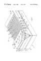
- FIG. 4illustrates a perspective, partially cut-away view of the multilevel electro-mechanical grating device 100 of the present invention.
- the multilevel electro-mechanical grating device 100 disclosed thereincan form at least three different levels.
- the mechanically deformable structuresare formed on top of a base 50 .
- the present embodiment as shown in FIG. 4discloses a device 100 that can be operated by the application of an electrostatic force. Because the actuation force of the multilevel electro-mechanical grating device 100 is electrostatic, the base 50 comprises several layers of different materials.
- the base 50comprises a substrate 52 , chosen from the materials glass and silicon, which is covered by a bottom conductive layer 56 .
- the thin bottom conductive layer 56is necessary since it acts as an electrode for applying the voltage to actuate the electro-mechanical grating device 100 .
- the thin bottom conductive layer 56is covered by a protective layer 58 .
- the bottom conductive layer 56is selected from the group consisting of aluminum, titanium, gold, silver, tungsten, silicon alloys and indium tin oxide.
- Above the protective layer 58a standoff layer 60 is formed which is followed by a spacer layer 65 .
- a ribbon layer 70is formed which is covered by a reflective layer 78 .
- the reflective layer 78also has to include a conductor in order to provide electrodes for the actuation of the multilevel electro-mechanical grating device 100 .
- the electrodesare patterned from the reflective and conductive layer 78 .
- the ribbon layer 70comprises a material with a suitably large tensile intrinsic stress such that the ribbons remain taut when no actuation force is applied. Examples of ribbon materials are silicon nitride, titanium aluminide, and titanium oxide. The thickness and tensile stress of the ribbon layer 70 are chosen to optimize performance by influencing the electrostatic or mechanic force required for actuation and the returning force, which affect the speed, resonance frequency, and voltage requirements of the multi-level mechanical grating device 100 .
- the spacer layer 65has a longitudinal channel 67 formed therein.
- the longitudinal channel 67extends along a longitudinal direction L—L of the multilevel electro-mechanical grating device 100 .
- the longitudinal channel 67comprises a first and second side wall 67 a and 67 b and a bottom 67 c.
- the channel 67is open to the top and covered by a first, a second and a third set of deformable ribbon elements 72 a , 72 b and 72 c .
- Each deformable ribbon element 72 a , 72 b and 72 cspans the channel 67 and is secured to the surface of the spacer layer 65 on either side of the channel 67 .
- the bottom 67 c of the channel 67is covered by the protective layer 58 .
- the ribbon layer 70is covered by the reflective layer 78 .
- the reflective layer 78which can be conductive as well, is patterned such that there are first and second conducting regions 78 a and 78 b , which form comb-like structures arranged on the surface in an interdigitated manner.
- a third conducting region 78 cis also created in the patterning of the reflective layer 78 .
- Thisis electrically connected to an electrical interconnect 82 , through an array of via openings 84 in an isolation layer 80 , which are filled with conducting material 86 .
- the first, second and third conductive regions 78 a , 78 b and 78 care mechanically and electrically isolated from one another.
- the ribbon layer 70is patterned to form first, second and third sets of deformable ribbon elements 72 a , 72 b and 72 c spanning the channel 67 .
- the first, second and third conducting regions 78 a , 78 b and 78 care electrically and mechanically isolated from one another, allowing separate application of actuation voltages to the first, second and third sets of ribbon elements 72 a , 72 b and 72 c .
- the deformable ribbon elements 72 a , 72 b and 72 care grouped according to the longitudinal direction L—L of the channel 67 . In the case of the three level electro-mechanical grating device 100 (embodiment as disclosed in FIG. 4 ), three deformable ribbon elements belong to one group.
- a plurality of standoffs 61is positioned on the bottom 67 c of the channel 67 .
- the standoffs 61are patterned from the standoff layer such that one standoff 61 is associated with one deformable ribbon element of each group. Furthermore, the standoffs are equidistantly spaced.
- each groupcomprises of a first, second and third ribbon element 73 L3 1 , 72 L3 2 , and 72 L3 3 .
- the standoffs 61are associated with the second ribbon element 72 L3 2 of each group (valid for three ribbon elements per group).
- the standoffs 61may also be patterned in the form of a single bar.
- FIG. 5A top view of the multilevel electro-mechanical grating device 100 with three levels is illustrated in FIG. 5, which also shows two planes perpendicular to the view illustrated.
- View Plane 6 — 6is a side view of the multilevel mechanical grating device 100 and depicts the view shown in FIG. 6 .
- View Plane 7 — 7is a side view of the device and depicts the view shown in FIG. 7 .
- Note that a device with four or more levels (four or more deformable ribbon elements per group)is a straightforward extension of the principles illustrated in FIGS. 5, 6 and 7 .
- the mechanical grating device 100as shown in FIG. 5, is a device which can be actuated by the application of an electrostatic force.
- the GLV described in FIGS. 5 and 6incorporates multiple levels, which means more than two, to discretely approximate a blazed grating.
- the intermediate levelscan be used to approximate blazed gratings for either the +1 or the ⁇ 1 diffracted order.
- the deviceacts as a reflective plane, reflecting light into the 0 order. Thus, light can be directed independently into three different angles, depending on which ribbons, if any, are actuated.
- FIGS. 7, 8 and 9illustrate this concept with three levels per group which means a first, a second and a third ribbon element 72 L3 1 , 72 L3 2 and 72 L3 3 per group
- FIGS. 10, 11 and 12illustrate the concept with four levels per group which means a first, a second, a third and a fourth ribbon element 72 L4 1 , 72 L4 2 72 L4 3 and 72 L4 4 per group
- the surface 53 a of the base 50is shown with the standoffs 61 (pedestals or lines) designed with specific heights as defined by the relationship between the height h 2 34 and the number of ribbons per period N.
- the value of Nis three for each period ⁇ , and only one intermediate level 54 a exists.
- the intermediate level 54 adefined by the upper surface 54 a of the standoffs 61 and should be ⁇ /6 above the surface 53 a of the base 50 to maximize the efficiency of diffraction into the +1 or ⁇ 1 order.
- FIG. 7The state of the GLV illustrated in FIG. 7 is achieved by not actuating any of the sets of ribbon elements 72 a , 72 b , or 72 c .
- the resultis nearly a planar mirrorlike surface, with an incident beam 90 being efficiently reflected into a zero order output beam 92 a with no diffraction into the ⁇ 1 orders.
- FIG. 8illustrates the state of the GLV that efficiently diffracts an incident beam 90 into a +1 order diffracted output beam 92 b, with no light diffracted into the 0 or ⁇ 1 orders. This is accomplished by actuating the first and second ribbon element 72 L3 1 and 72 L3 2 . According to the actuation, the levels 64 b , 54 b and 53 b are generated.
- FIG. 9illustrates the state of the GLV that efficiently diffracts an incident beam 90 into a ⁇ 1 order diffracted output beam 92 c , with no light diffracted into the 0 or +1 orders. This is accomplished by actuating the second and third ribbon elements 72 L3 2 and 72 L3 3 .
- the switching from the +1 order diffraction to the ⁇ 1 order diffractioncan be accomplished by turning off the voltage applied to the first ribbon element 72 L3 1 per group, by leaving on the voltage applied to the second ribbon element 72 L3 2 per group and by applying a voltage to the third ribbon element 72 L3 3 per group.
- FIGS. 10, 11 and 12are comparable to FIGS. 7, 8 and 9 , except that four ribbons belong to one group.
- a first set of standoffs 61 1defines intermediate levels 54 a and a second set of standoffs 61 2 defines the intermediate levels 55 a. Intermediate levels 54 a and 55 a are spaced by h 2 38 .
- the first, second and third ribbon elements 72 74 1 , 72 L4 2 and 72 L4 3 of each groupare actuated such that their top surfaces are level with 53 b , 54 b and 55 b respectively.
- FIG. 10A first set of standoffs 61 1 defines intermediate levels 54 a and a second set of standoffs 61 2 defines the intermediate levels 55 a. Intermediate levels 54 a and 55 a are spaced by h 2 38 .
- the first, second and third ribbon elements 72 74 1 , 72 L4 2 and 72 L4 3 of each groupare actuated such that their top surfaces are level with 53 b , 54 b and 55 b respectively.
- the first, third and fourth ribbon elements 72 L4 1 , 72 L4 3 and 72 L4 4 of each groupare actuated such that their top surfaces are level with 53 b , 55 b and 54 b respectively.
- a switching between the +1 order diffraction and the ⁇ 1 order diffractionis simply caused by turning off the voltage applied to the second ribbon element 72 L4 2 of each group and turning on the voltage applied to the fourth ribbon element 72 L4 4 of each group, while continuously applying voltage to the first and third ribbon elements 72 L4 1 and 72 L4 3 of each group.
- the lower standoff level 54 a of the first set of standoffs 61 1is ⁇ /8 above the substrate surface 53 a
- the upper level 55 a of the second set of standoffs 61 2is ⁇ /4 above the substrate level 53 a.
- the total depth of the channel 67defined as the separation of levels 64 a and 53 a , is equal to 3 ⁇ /8. In general, the total depth of the channel 67 should be (1 ⁇ 1/N) ⁇ /2.
- One methodis to increase the contrast of the modulator by switching between the +1 order configuration shown in FIGS. 8 and 11, and the ⁇ 1 order configuration shown in FIGS. 9 and 12.
- the second methodis to relax the fabrication difficulties by producing larger pitch gratings that switch between the +1 order and ⁇ 1 order configurations.
- the last methodis to utilize all three configurations, the 0 order configuration illustrated in FIGS. 7 and 10, and the +1 order and ⁇ 1 order configurations, to produce a three-way light valve.
- the first methodutilizes the fact that light collected from the GLV modulator must be filtered to remove the light coming from the unactuated grating elements. This is typically accomplished by placing a slit (not shown) in the farfield or the focal plane of an imaging lens (not shown). However, it is well known to one skilled in the art that placing a slit in the focal plane of an imaging lens will result in a loss of fidelity of the image. Thus, in order to accurately image the GLV array with high fidelity, the slit must have a minimum width. In a conventional GLV modulator though, the light from the unactuated grating elements in the 0 diffracted order may not be sufficiently separated in angle from the desired +1 diffracted order. The consequence is that a portion of the unwanted light can pass through the spatial filter, thereby reducing the contrast of the modulator (defined as the ratio of the intensity from a grating element in its actuated state to that in its unactuated state).
- the first method of this inventionmodulating by switching between the +1 diffraction order configuration and the ⁇ 1 diffraction order configuration, presents an improvement to this problem.
- the angular separation between the desired and undesired output beamsis doubled as compared to the conventional mode of operation.
- the resultis that substantially less unwanted light can pass through a spatial filter with the necessary dimensions for image fidelity.
- the contrastcan be improved, both by the higher efficiency of diffraction of the desired light due to the multilevel grating configuration, and by the reduction in unwanted light by increased angular separation.
- the second method presentedis a means of using the larger angular separation to relax the fabrication difficulties by designing multilevel gratings with larger pitches. If the grating pitch is desired to be kept constant, increasing the number of ribbons N per grating period leads to increased difficulty in the photolithography steps. Specifically, the width of the gaps between ribbons (typically near the resolution limit of the photolithography process) becomes a more significant fraction of the ribbon width as a larger number of ribbons is formed within the same grating period. This can lead to a reduction in diffraction efficiency.
- FIGS. 13 and 14each illustrate two elements, one turned off and the other on, of two different grating modulators.
- FIG. 14shows two elements from a 4-level grating modulator 102 with intermediate levels defined according to the same methods used in device 49 a illustrated in FIG. 10 .
- the device in FIG. 14shows two elements from a 4-level grating modulator 102 with intermediate levels defined according to the same methods used in device 49 a illustrated in FIG. 10 .
- the device in FIG. 14shows two elements from a 4-level grating modulator 102 with intermediate levels defined according to the same methods used in device 49 a illustrated in FIG. 10 .
- the grating modulator in FIG. 14will provide nearly the same angular separation of the “on” and “off” output beams as the modulator in FIG. 13, while approximately doubling the efficiency of diffraction.
- the last application of this inventionis to use all three independent outputs to form a three-way light valve.
- Such a devicewould be useful, for example, in a system equipped with an auxiliary optical system, e.g. to monitor device performance.
- the systemcould be arranged with the +1 output beam being directed to the target (screen or printing medium), and the ⁇ 1 order output beam being directed to the auxiliary optical system. While in principle this could be accomplished with a conventional bi-level grating light valve, light cannot be switched independently into either the +1 or ⁇ 1 order diffracted beam in that configuration.
Landscapes
- Physics & Mathematics (AREA)
- General Physics & Mathematics (AREA)
- Optics & Photonics (AREA)
- Mechanical Light Control Or Optical Switches (AREA)
Abstract
Description


| TABLE 1 | |||||||||
| N | η−3 | η−2 | η−1 | η0 | η1 | η2 | η3 | ||
| 2 | 0.045 | 0 | 0.405 | 0 | 0.405 | 0 | 0.045 | ||
| 3 | 0 | 0.171 | 0 | 0 | 0.684 | 0 | 0 | ||
| 4 | 0.090 | 0 | 0 | 0 | 0.811 | 0 | 0 | ||
| 5 | 0 | 0 | 0 | 0 | 0.875 | 0 | 0 | ||
| PARTS LIST |
| 10 | reflective grating | ||
| 11 | angle θ0 | ||
| 12 | optical beam | ||
| 13 | period Λ | ||
| 14 | width of the groove L1 | ||
| 15 | angle θm | ||
| 16 | diffracted beam | ||
| 20 | blazed grating | ||
| 22 | incident beam | ||
| 24 | grating surface | ||
| 26a to 26f | diffracted beams | ||
| 30 | grating profile | ||
| 32 | continuous blazed grating profile | ||
| 34 | width L2 | ||
| 38 | a height of separation h2 | ||
| 50 | base | ||
| 52 | substrate | ||
| 53 | surface of the base | ||
| 53a | surface | ||
| 53b | level | ||
| 54a | top surface of standoffs | ||
| 54b | second intermediate top level | ||
| 55a | surface | ||
| 55b | first intermediate top level | ||
| 56 | bottom conductive layer | ||
| 56a | surface of the bottom conductive layer | ||
| 58 | protective layer | ||
| 60 | standoff layer | ||
| 61 | standoff | ||
| 611 | first set of standoffs | ||
| 612 | second set of standoffs | ||
| 64a | first bottom level | ||
| 64b | first top level | ||
| 65 | spacer layer | ||
| 67 | channel | ||
| 67a | first side wall of the channel | ||
| 67b | second side wall of the channel | ||
| 67c | bottom of the channel | ||
| 70 | ribbon layer | ||
| 70a | bottom surface of the coplanar ribbon elements | ||
| 70b | top surface of the coplanar ribbon elements | ||
| 72a | first set of deformable ribbon elements | ||
| 72b | second set of deformable ribbon elements | ||
| 72c | third set of deformable ribbon elements | ||
| 72L31 | first element of each group of three | ||
| 72L32 | second element of each group of three | ||
| 72L33 | third element of each group of three | ||
| 72L41 | first element of each group of four | ||
| 72L42 | second element of each group of four | ||
| 72L43 | third element of each group of four | ||
| 72L44 | fourth ribbon element of each group of four | ||
| 78 | first conductive layer | ||
| 78a | first conducting region | ||
| 78b | second conducting region | ||
| 78c | third conducting region | ||
| 80 | isolation layer | ||
| 82 | electrical interconnect | ||
| 84 | via opening | ||
| 86 | conducting material | ||
| 90 | bi-level grating | ||
| 92 | width Lrof ribbons | ||
| 92b | diffracted beam | ||
| 94 | “on” bi-level grating element | ||
| 96 | “off” bi-level grating element | ||
| 98a | diffraction into the +1 order | ||
| 98b | diffraction into the −1 order | ||
| 98c | diffraction into the 0 order | ||
| 99 | θsangular separation | ||
| 100 | multilevel electro-mechanical grating device | ||
| 104 | “on” grating element (four level) | ||
| 106 | “off” grating element (four level) | ||
| 108a | diffraction into the +1 order | ||
| 108b | diffraction into the −1 order | ||
| 110 | θsangular separation | ||
| L | longitudinal direction | ||
| N | number of discrete steps | ||
| d | grating depth | ||
| m | order | ||
| n | number of levels | ||
| Λ | pitch | ||
| ηm | diffraction efficiency | ||
| 6-6 | view plane | ||
| 7-7 | view plane | ||
| L-L | longitudinal direction of the device | ||
| O-O | orthogonal axis | ||
Claims (21)


Priority Applications (1)
| Application Number | Priority Date | Filing Date | Title |
|---|---|---|---|
| US09/216,559US6172796B1 (en) | 1998-12-18 | 1998-12-18 | Multilevel electro-mechanical grating device and a method for operating a multilevel mechanical and electro-mechanical grating device |
Applications Claiming Priority (1)
| Application Number | Priority Date | Filing Date | Title |
|---|---|---|---|
| US09/216,559US6172796B1 (en) | 1998-12-18 | 1998-12-18 | Multilevel electro-mechanical grating device and a method for operating a multilevel mechanical and electro-mechanical grating device |
Publications (1)
| Publication Number | Publication Date |
|---|---|
| US6172796B1true US6172796B1 (en) | 2001-01-09 |
Family
ID=22807533
Family Applications (1)
| Application Number | Title | Priority Date | Filing Date |
|---|---|---|---|
| US09/216,559Expired - LifetimeUS6172796B1 (en) | 1998-12-18 | 1998-12-18 | Multilevel electro-mechanical grating device and a method for operating a multilevel mechanical and electro-mechanical grating device |
Country Status (1)
| Country | Link |
|---|---|
| US (1) | US6172796B1 (en) |
Cited By (62)
| Publication number | Priority date | Publication date | Assignee | Title |
|---|---|---|---|---|
| US6243194B1 (en)* | 1998-12-18 | 2001-06-05 | Eastman Kodak Company | Electro-mechanical grating device |
| US6282012B1 (en)* | 1999-12-10 | 2001-08-28 | Eastman Kodak Company | Method for damping ribbon elements in a micromechanical grating device by selection of actuation waveform |
| US6329738B1 (en) | 1999-03-30 | 2001-12-11 | Massachusetts Institute Of Technology | Precision electrostatic actuation and positioning |
| US6335831B2 (en) | 1998-12-18 | 2002-01-01 | Eastman Kodak Company | Multilevel mechanical grating device |
| WO2002005010A1 (en)* | 2000-07-10 | 2002-01-17 | Opts, Inc. | Grating type spatial light modulators and method of manufacturing grating type spatial light modulators |
| US6445502B1 (en)* | 2001-02-02 | 2002-09-03 | Celeste Optics, Inc. | Variable blazed grating |
| US20020167695A1 (en)* | 2001-03-02 | 2002-11-14 | Senturia Stephen D. | Methods and apparatus for diffractive optical processing using an actuatable structure |
| US20030038943A1 (en)* | 2001-08-21 | 2003-02-27 | Kais Almarzouk | Method and apparatus for measuring wavelength jitter of light signal |
| WO2003021338A3 (en)* | 2001-08-15 | 2003-07-03 | Silicon Light Machines Inc | Blazed grating light valve |
| US6618187B2 (en)* | 2000-07-13 | 2003-09-09 | Creo Il. Ltd. | Blazed micro-mechanical light modulator and array thereof |
| WO2003060597A3 (en)* | 2001-12-21 | 2003-10-23 | Polychromix Corp | Method and apparatus providing reduced polarization-dependent loss |
| US6639722B2 (en)* | 2001-08-15 | 2003-10-28 | Silicon Light Machines | Stress tuned blazed grating light valve |
| EP1245969A3 (en)* | 2001-03-29 | 2003-12-17 | Eastman Kodak Company | Electromechanical conformal grating device with improved optical efficiency and contrast |
| US20040035821A1 (en)* | 1999-10-26 | 2004-02-26 | Doan Jonathan C. | Methods for forming and releasing microelectromechanical structures |
| US6707591B2 (en) | 2001-04-10 | 2004-03-16 | Silicon Light Machines | Angled illumination for a single order light modulator based projection system |
| US6714337B1 (en) | 2002-06-28 | 2004-03-30 | Silicon Light Machines | Method and device for modulating a light beam and having an improved gamma response |
| US6712480B1 (en) | 2002-09-27 | 2004-03-30 | Silicon Light Machines | Controlled curvature of stressed micro-structures |
| US6721473B1 (en) | 2001-02-02 | 2004-04-13 | Cheetah Omni, Llc | Variable blazed grating based signal processing |
| US6724125B2 (en) | 1999-03-30 | 2004-04-20 | Massachusetts Institute Of Technology | Methods and apparatus for diffractive optical processing using an actuatable structure |
| US6764875B2 (en) | 1998-07-29 | 2004-07-20 | Silicon Light Machines | Method of and apparatus for sealing an hermetic lid to a semiconductor die |
| US6767751B2 (en) | 2002-05-28 | 2004-07-27 | Silicon Light Machines, Inc. | Integrated driver process flow |
| US6782205B2 (en) | 2001-06-25 | 2004-08-24 | Silicon Light Machines | Method and apparatus for dynamic equalization in wavelength division multiplexing |
| US6801354B1 (en)* | 2002-08-20 | 2004-10-05 | Silicon Light Machines, Inc. | 2-D diffraction grating for substantially eliminating polarization dependent losses |
| US6800238B1 (en) | 2002-01-15 | 2004-10-05 | Silicon Light Machines, Inc. | Method for domain patterning in low coercive field ferroelectrics |
| US6806997B1 (en) | 2003-02-28 | 2004-10-19 | Silicon Light Machines, Inc. | Patterned diffractive light modulator ribbon for PDL reduction |
| US6813059B2 (en) | 2002-06-28 | 2004-11-02 | Silicon Light Machines, Inc. | Reduced formation of asperities in contact micro-structures |
| US6822797B1 (en) | 2002-05-31 | 2004-11-23 | Silicon Light Machines, Inc. | Light modulator structure for producing high-contrast operation using zero-order light |
| US6829077B1 (en) | 2003-02-28 | 2004-12-07 | Silicon Light Machines, Inc. | Diffractive light modulator with dynamically rotatable diffraction plane |
| US6829258B1 (en) | 2002-06-26 | 2004-12-07 | Silicon Light Machines, Inc. | Rapidly tunable external cavity laser |
| US6865346B1 (en) | 2001-06-05 | 2005-03-08 | Silicon Light Machines Corporation | Fiber optic transceiver |
| US6872984B1 (en) | 1998-07-29 | 2005-03-29 | Silicon Light Machines Corporation | Method of sealing a hermetic lid to a semiconductor die at an angle |
| KR100486495B1 (en)* | 2001-09-28 | 2005-04-29 | 엘지전자 주식회사 | Optical modulator and manufacturing method for thereof |
| US6908201B2 (en) | 2002-06-28 | 2005-06-21 | Silicon Light Machines Corporation | Micro-support structures |
| US20050134302A1 (en)* | 2003-12-18 | 2005-06-23 | Hao Pan | Dynamic gamma for a liquid crystal display |
| US6922273B1 (en) | 2003-02-28 | 2005-07-26 | Silicon Light Machines Corporation | PDL mitigation structure for diffractive MEMS and gratings |
| US6922272B1 (en) | 2003-02-14 | 2005-07-26 | Silicon Light Machines Corporation | Method and apparatus for leveling thermal stress variations in multi-layer MEMS devices |
| US6927891B1 (en)* | 2002-12-23 | 2005-08-09 | Silicon Light Machines Corporation | Tilt-able grating plane for improved crosstalk in 1×N blaze switches |
| US6928207B1 (en) | 2002-12-12 | 2005-08-09 | Silicon Light Machines Corporation | Apparatus for selectively blocking WDM channels |
| US6934070B1 (en) | 2002-12-18 | 2005-08-23 | Silicon Light Machines Corporation | Chirped optical MEM device |
| US6947613B1 (en) | 2003-02-11 | 2005-09-20 | Silicon Light Machines Corporation | Wavelength selective switch and equalizer |
| US6956878B1 (en) | 2000-02-07 | 2005-10-18 | Silicon Light Machines Corporation | Method and apparatus for reducing laser speckle using polarization averaging |
| US6956995B1 (en) | 2001-11-09 | 2005-10-18 | Silicon Light Machines Corporation | Optical communication arrangement |
| US6967718B1 (en) | 2003-02-28 | 2005-11-22 | Silicon Light Machines Corportion | Method and apparatus for monitoring WDM channels and for analyzing dispersed spectrum of light |
| US6987600B1 (en) | 2002-12-17 | 2006-01-17 | Silicon Light Machines Corporation | Arbitrary phase profile for better equalization in dynamic gain equalizer |
| US6991953B1 (en) | 2001-09-13 | 2006-01-31 | Silicon Light Machines Corporation | Microelectronic mechanical system and methods |
| US7027202B1 (en) | 2003-02-28 | 2006-04-11 | Silicon Light Machines Corp | Silicon substrate as a light modulator sacrificial layer |
| US7042611B1 (en) | 2003-03-03 | 2006-05-09 | Silicon Light Machines Corporation | Pre-deflected bias ribbons |
| US7043110B1 (en)* | 2002-12-10 | 2006-05-09 | Silicon Light Machines Corporation | Wavelength-selective switch and equalizer |
| US7046410B2 (en) | 2001-10-11 | 2006-05-16 | Polychromix, Inc. | Actuatable diffractive optical processor |
| US7057819B1 (en) | 2002-12-17 | 2006-06-06 | Silicon Light Machines Corporation | High contrast tilting ribbon blazed grating |
| US7057795B2 (en) | 2002-08-20 | 2006-06-06 | Silicon Light Machines Corporation | Micro-structures with individually addressable ribbon pairs |
| US7068372B1 (en) | 2003-01-28 | 2006-06-27 | Silicon Light Machines Corporation | MEMS interferometer-based reconfigurable optical add-and-drop multiplexor |
| US7116862B1 (en) | 2000-12-22 | 2006-10-03 | Cheetah Omni, Llc | Apparatus and method for providing gain equalization |
| US7177081B2 (en) | 2001-03-08 | 2007-02-13 | Silicon Light Machines Corporation | High contrast grating light valve type device |
| US20070086780A1 (en)* | 2001-02-02 | 2007-04-19 | Cheetah Omni, Llc | Optical Logic Gate Based Optical Router |
| US20070101398A1 (en)* | 2005-11-01 | 2007-05-03 | Cheetah Omni, Llc | Packet-Based Digital Display System |
| US20070194239A1 (en)* | 2006-01-31 | 2007-08-23 | Mcallister Abraham | Apparatus and method providing a hand-held spectrometer |
| US7286764B1 (en) | 2003-02-03 | 2007-10-23 | Silicon Light Machines Corporation | Reconfigurable modulator-based optical add-and-drop multiplexer |
| US7339714B1 (en) | 2001-02-02 | 2008-03-04 | Cheetah Omni, Llc | Variable blazed grating based signal processing |
| US20080075460A1 (en)* | 2001-12-03 | 2008-03-27 | Islam Mohammed N | Method and Apparatus for Scheduling Communication using a Star Switching Fabric |
| US7391973B1 (en) | 2003-02-28 | 2008-06-24 | Silicon Light Machines Corporation | Two-stage gain equalizer |
| EP1579263B1 (en)* | 2002-12-30 | 2010-12-01 | Sinvent AS | Configurable diffractive optical element |
Citations (10)
| Publication number | Priority date | Publication date | Assignee | Title |
|---|---|---|---|---|
| US4011009A (en) | 1975-05-27 | 1977-03-08 | Xerox Corporation | Reflection diffraction grating having a controllable blaze angle |
| US4492435A (en) | 1982-07-02 | 1985-01-08 | Xerox Corporation | Multiple array full width electro mechanical modulator |
| US4596992A (en) | 1984-08-31 | 1986-06-24 | Texas Instruments Incorporated | Linear spatial light modulator and printer |
| US5115344A (en) | 1990-10-03 | 1992-05-19 | Motorola, Inc. | Tunable diffraction grating |
| US5311360A (en) | 1992-04-28 | 1994-05-10 | The Board Of Trustees Of The Leland Stanford, Junior University | Method and apparatus for modulating a light beam |
| US5661593A (en) | 1992-10-01 | 1997-08-26 | Engle; Craig D. | Linear electrostatic modulator |
| US5757536A (en) | 1995-08-30 | 1998-05-26 | Sandia Corporation | Electrically-programmable diffraction grating |
| US5808797A (en) | 1992-04-28 | 1998-09-15 | Silicon Light Machines | Method and apparatus for modulating a light beam |
| US5949570A (en)* | 1995-06-20 | 1999-09-07 | Matsushita Electric Industrial Co., Ltd. | Diffractive optical modulator and method for producing the same, infrared sensor including such a diffractive optical modulator and method for producing the same, and display device including such a diffractive optical modulator |
| US5999319A (en)* | 1997-05-02 | 1999-12-07 | Interscience, Inc. | Reconfigurable compound diffraction grating |
- 1998
- 1998-12-18USUS09/216,559patent/US6172796B1/ennot_activeExpired - Lifetime
Patent Citations (12)
| Publication number | Priority date | Publication date | Assignee | Title |
|---|---|---|---|---|
| US4011009A (en) | 1975-05-27 | 1977-03-08 | Xerox Corporation | Reflection diffraction grating having a controllable blaze angle |
| US4492435A (en) | 1982-07-02 | 1985-01-08 | Xerox Corporation | Multiple array full width electro mechanical modulator |
| US4596992A (en) | 1984-08-31 | 1986-06-24 | Texas Instruments Incorporated | Linear spatial light modulator and printer |
| US5115344A (en) | 1990-10-03 | 1992-05-19 | Motorola, Inc. | Tunable diffraction grating |
| US5311360A (en) | 1992-04-28 | 1994-05-10 | The Board Of Trustees Of The Leland Stanford, Junior University | Method and apparatus for modulating a light beam |
| US5459610A (en) | 1992-04-28 | 1995-10-17 | The Board Of Trustees Of The Leland Stanford, Junior University | Deformable grating apparatus for modulating a light beam and including means for obviating stiction between grating elements and underlying substrate |
| US5677783A (en) | 1992-04-28 | 1997-10-14 | The Board Of Trustees Of The Leland Stanford, Junior University | Method of making a deformable grating apparatus for modulating a light beam and including means for obviating stiction between grating elements and underlying substrate |
| US5808797A (en) | 1992-04-28 | 1998-09-15 | Silicon Light Machines | Method and apparatus for modulating a light beam |
| US5661593A (en) | 1992-10-01 | 1997-08-26 | Engle; Craig D. | Linear electrostatic modulator |
| US5949570A (en)* | 1995-06-20 | 1999-09-07 | Matsushita Electric Industrial Co., Ltd. | Diffractive optical modulator and method for producing the same, infrared sensor including such a diffractive optical modulator and method for producing the same, and display device including such a diffractive optical modulator |
| US5757536A (en) | 1995-08-30 | 1998-05-26 | Sandia Corporation | Electrically-programmable diffraction grating |
| US5999319A (en)* | 1997-05-02 | 1999-12-07 | Interscience, Inc. | Reconfigurable compound diffraction grating |
Cited By (79)
| Publication number | Priority date | Publication date | Assignee | Title |
|---|---|---|---|---|
| US6764875B2 (en) | 1998-07-29 | 2004-07-20 | Silicon Light Machines | Method of and apparatus for sealing an hermetic lid to a semiconductor die |
| US6872984B1 (en) | 1998-07-29 | 2005-03-29 | Silicon Light Machines Corporation | Method of sealing a hermetic lid to a semiconductor die at an angle |
| US6243194B1 (en)* | 1998-12-18 | 2001-06-05 | Eastman Kodak Company | Electro-mechanical grating device |
| US6335831B2 (en) | 1998-12-18 | 2002-01-01 | Eastman Kodak Company | Multilevel mechanical grating device |
| US6724125B2 (en) | 1999-03-30 | 2004-04-20 | Massachusetts Institute Of Technology | Methods and apparatus for diffractive optical processing using an actuatable structure |
| US6329738B1 (en) | 1999-03-30 | 2001-12-11 | Massachusetts Institute Of Technology | Precision electrostatic actuation and positioning |
| US6960305B2 (en) | 1999-10-26 | 2005-11-01 | Reflectivity, Inc | Methods for forming and releasing microelectromechanical structures |
| US20040035821A1 (en)* | 1999-10-26 | 2004-02-26 | Doan Jonathan C. | Methods for forming and releasing microelectromechanical structures |
| US6282012B1 (en)* | 1999-12-10 | 2001-08-28 | Eastman Kodak Company | Method for damping ribbon elements in a micromechanical grating device by selection of actuation waveform |
| US6956878B1 (en) | 2000-02-07 | 2005-10-18 | Silicon Light Machines Corporation | Method and apparatus for reducing laser speckle using polarization averaging |
| WO2002005010A1 (en)* | 2000-07-10 | 2002-01-17 | Opts, Inc. | Grating type spatial light modulators and method of manufacturing grating type spatial light modulators |
| US6618187B2 (en)* | 2000-07-13 | 2003-09-09 | Creo Il. Ltd. | Blazed micro-mechanical light modulator and array thereof |
| US7116862B1 (en) | 2000-12-22 | 2006-10-03 | Cheetah Omni, Llc | Apparatus and method for providing gain equalization |
| US6900919B1 (en) | 2001-02-02 | 2005-05-31 | Cheetah Omni, Llc | Variable blazed grating |
| US20070086780A1 (en)* | 2001-02-02 | 2007-04-19 | Cheetah Omni, Llc | Optical Logic Gate Based Optical Router |
| US6445502B1 (en)* | 2001-02-02 | 2002-09-03 | Celeste Optics, Inc. | Variable blazed grating |
| US6972886B2 (en) | 2001-02-02 | 2005-12-06 | Cheetah Omni, Llc | Variable blazed grating |
| US7522836B2 (en) | 2001-02-02 | 2009-04-21 | Cheetah Omni, Llc | Optical logic gate based optical router |
| US6721473B1 (en) | 2001-02-02 | 2004-04-13 | Cheetah Omni, Llc | Variable blazed grating based signal processing |
| US20050099692A1 (en)* | 2001-02-02 | 2005-05-12 | Cheetah Omni, Inc., A Texas Limited Liability Company | Variable blazed grating |
| US6847479B1 (en) | 2001-02-02 | 2005-01-25 | Cheetah Omni, Llc | Variable blazed grating |
| US6844974B1 (en) | 2001-02-02 | 2005-01-18 | Cheetah Omni, Llc | Variable blazed grating |
| US7339714B1 (en) | 2001-02-02 | 2008-03-04 | Cheetah Omni, Llc | Variable blazed grating based signal processing |
| US20020167695A1 (en)* | 2001-03-02 | 2002-11-14 | Senturia Stephen D. | Methods and apparatus for diffractive optical processing using an actuatable structure |
| US7177081B2 (en) | 2001-03-08 | 2007-02-13 | Silicon Light Machines Corporation | High contrast grating light valve type device |
| EP1245969A3 (en)* | 2001-03-29 | 2003-12-17 | Eastman Kodak Company | Electromechanical conformal grating device with improved optical efficiency and contrast |
| US6707591B2 (en) | 2001-04-10 | 2004-03-16 | Silicon Light Machines | Angled illumination for a single order light modulator based projection system |
| US6865346B1 (en) | 2001-06-05 | 2005-03-08 | Silicon Light Machines Corporation | Fiber optic transceiver |
| US6782205B2 (en) | 2001-06-25 | 2004-08-24 | Silicon Light Machines | Method and apparatus for dynamic equalization in wavelength division multiplexing |
| WO2003021338A3 (en)* | 2001-08-15 | 2003-07-03 | Silicon Light Machines Inc | Blazed grating light valve |
| EP1417528A4 (en)* | 2001-08-15 | 2005-08-03 | Silicon Light Machines Inc | Blazed grating light valve |
| US6639722B2 (en)* | 2001-08-15 | 2003-10-28 | Silicon Light Machines | Stress tuned blazed grating light valve |
| CN100378495C (en)* | 2001-08-15 | 2008-04-02 | 硅光机器公司 | Luminous grating light valve |
| US6785001B2 (en) | 2001-08-21 | 2004-08-31 | Silicon Light Machines, Inc. | Method and apparatus for measuring wavelength jitter of light signal |
| US20030038943A1 (en)* | 2001-08-21 | 2003-02-27 | Kais Almarzouk | Method and apparatus for measuring wavelength jitter of light signal |
| US6991953B1 (en) | 2001-09-13 | 2006-01-31 | Silicon Light Machines Corporation | Microelectronic mechanical system and methods |
| US7049164B2 (en) | 2001-09-13 | 2006-05-23 | Silicon Light Machines Corporation | Microelectronic mechanical system and methods |
| KR100486495B1 (en)* | 2001-09-28 | 2005-04-29 | 엘지전자 주식회사 | Optical modulator and manufacturing method for thereof |
| US7046410B2 (en) | 2001-10-11 | 2006-05-16 | Polychromix, Inc. | Actuatable diffractive optical processor |
| US6956995B1 (en) | 2001-11-09 | 2005-10-18 | Silicon Light Machines Corporation | Optical communication arrangement |
| US20080075460A1 (en)* | 2001-12-03 | 2008-03-27 | Islam Mohammed N | Method and Apparatus for Scheduling Communication using a Star Switching Fabric |
| US20040027667A1 (en)* | 2001-12-21 | 2004-02-12 | Deutsch Erik R. | Method and apparatus providing reduced polarization-dependent loss |
| EP1459123A4 (en)* | 2001-12-21 | 2007-05-23 | Polychromix Corp | Method and apparatus providing reduced polarization;dependent loss |
| WO2003060597A3 (en)* | 2001-12-21 | 2003-10-23 | Polychromix Corp | Method and apparatus providing reduced polarization-dependent loss |
| US6768589B2 (en)* | 2001-12-21 | 2004-07-27 | Polychromix Corporation | Method and apparatus providing reduced polarization-dependent loss |
| US6800238B1 (en) | 2002-01-15 | 2004-10-05 | Silicon Light Machines, Inc. | Method for domain patterning in low coercive field ferroelectrics |
| US6767751B2 (en) | 2002-05-28 | 2004-07-27 | Silicon Light Machines, Inc. | Integrated driver process flow |
| US6822797B1 (en) | 2002-05-31 | 2004-11-23 | Silicon Light Machines, Inc. | Light modulator structure for producing high-contrast operation using zero-order light |
| US6829258B1 (en) | 2002-06-26 | 2004-12-07 | Silicon Light Machines, Inc. | Rapidly tunable external cavity laser |
| US6714337B1 (en) | 2002-06-28 | 2004-03-30 | Silicon Light Machines | Method and device for modulating a light beam and having an improved gamma response |
| US6908201B2 (en) | 2002-06-28 | 2005-06-21 | Silicon Light Machines Corporation | Micro-support structures |
| US6813059B2 (en) | 2002-06-28 | 2004-11-02 | Silicon Light Machines, Inc. | Reduced formation of asperities in contact micro-structures |
| US7057795B2 (en) | 2002-08-20 | 2006-06-06 | Silicon Light Machines Corporation | Micro-structures with individually addressable ribbon pairs |
| US6801354B1 (en)* | 2002-08-20 | 2004-10-05 | Silicon Light Machines, Inc. | 2-D diffraction grating for substantially eliminating polarization dependent losses |
| US6712480B1 (en) | 2002-09-27 | 2004-03-30 | Silicon Light Machines | Controlled curvature of stressed micro-structures |
| US7043110B1 (en)* | 2002-12-10 | 2006-05-09 | Silicon Light Machines Corporation | Wavelength-selective switch and equalizer |
| US6928207B1 (en) | 2002-12-12 | 2005-08-09 | Silicon Light Machines Corporation | Apparatus for selectively blocking WDM channels |
| US7057819B1 (en) | 2002-12-17 | 2006-06-06 | Silicon Light Machines Corporation | High contrast tilting ribbon blazed grating |
| US6987600B1 (en) | 2002-12-17 | 2006-01-17 | Silicon Light Machines Corporation | Arbitrary phase profile for better equalization in dynamic gain equalizer |
| US6934070B1 (en) | 2002-12-18 | 2005-08-23 | Silicon Light Machines Corporation | Chirped optical MEM device |
| US6927891B1 (en)* | 2002-12-23 | 2005-08-09 | Silicon Light Machines Corporation | Tilt-able grating plane for improved crosstalk in 1×N blaze switches |
| EP1579263B1 (en)* | 2002-12-30 | 2010-12-01 | Sinvent AS | Configurable diffractive optical element |
| US7068372B1 (en) | 2003-01-28 | 2006-06-27 | Silicon Light Machines Corporation | MEMS interferometer-based reconfigurable optical add-and-drop multiplexor |
| US7286764B1 (en) | 2003-02-03 | 2007-10-23 | Silicon Light Machines Corporation | Reconfigurable modulator-based optical add-and-drop multiplexer |
| US6947613B1 (en) | 2003-02-11 | 2005-09-20 | Silicon Light Machines Corporation | Wavelength selective switch and equalizer |
| US6922272B1 (en) | 2003-02-14 | 2005-07-26 | Silicon Light Machines Corporation | Method and apparatus for leveling thermal stress variations in multi-layer MEMS devices |
| US6922273B1 (en) | 2003-02-28 | 2005-07-26 | Silicon Light Machines Corporation | PDL mitigation structure for diffractive MEMS and gratings |
| US6829077B1 (en) | 2003-02-28 | 2004-12-07 | Silicon Light Machines, Inc. | Diffractive light modulator with dynamically rotatable diffraction plane |
| US6806997B1 (en) | 2003-02-28 | 2004-10-19 | Silicon Light Machines, Inc. | Patterned diffractive light modulator ribbon for PDL reduction |
| US7391973B1 (en) | 2003-02-28 | 2008-06-24 | Silicon Light Machines Corporation | Two-stage gain equalizer |
| US7027202B1 (en) | 2003-02-28 | 2006-04-11 | Silicon Light Machines Corp | Silicon substrate as a light modulator sacrificial layer |
| US6967718B1 (en) | 2003-02-28 | 2005-11-22 | Silicon Light Machines Corportion | Method and apparatus for monitoring WDM channels and for analyzing dispersed spectrum of light |
| US7042611B1 (en) | 2003-03-03 | 2006-05-09 | Silicon Light Machines Corporation | Pre-deflected bias ribbons |
| US20050134302A1 (en)* | 2003-12-18 | 2005-06-23 | Hao Pan | Dynamic gamma for a liquid crystal display |
| US20070101398A1 (en)* | 2005-11-01 | 2007-05-03 | Cheetah Omni, Llc | Packet-Based Digital Display System |
| US7429983B2 (en) | 2005-11-01 | 2008-09-30 | Cheetah Omni, Llc | Packet-based digital display system |
| US8379061B2 (en) | 2005-11-01 | 2013-02-19 | Gopala Solutions Limited Liability Company | Packet-based digital display system |
| US20070194239A1 (en)* | 2006-01-31 | 2007-08-23 | Mcallister Abraham | Apparatus and method providing a hand-held spectrometer |
| US7791027B2 (en) | 2006-01-31 | 2010-09-07 | Ahura Scientific Inc. | Apparatus and method providing a hand-held spectrometer |
Similar Documents
| Publication | Publication Date | Title |
|---|---|---|
| US6172796B1 (en) | Multilevel electro-mechanical grating device and a method for operating a multilevel mechanical and electro-mechanical grating device | |
| US6335831B2 (en) | Multilevel mechanical grating device | |
| US6181458B1 (en) | Mechanical grating device with optical coating and method of making mechanical grating device with optical coating | |
| US5999319A (en) | Reconfigurable compound diffraction grating | |
| US6663788B2 (en) | Method for manufacturing a mechanical conformal grating device | |
| EP1143287B1 (en) | Method and system for calibrating a diffractive grating modulator | |
| US6061166A (en) | Diffractive light modulator | |
| US6836352B2 (en) | High frequency deformable mirror device | |
| EP1014117B1 (en) | A mechanical grating device | |
| US6829092B2 (en) | Blazed grating light valve | |
| US5757536A (en) | Electrically-programmable diffraction grating | |
| KR960001796A (en) | Rotary light regulators and methods of manufacturing such diffractive light regulators, infrared sensors comprising such diffractive light regulators, methods of manufacturing such infrared detectors, and display devices comprising such diffractive light regulators | |
| US6243194B1 (en) | Electro-mechanical grating device | |
| US6894836B2 (en) | Diffraction grating, method of making and method of using | |
| KR20060091595A (en) | Color display device using 1 panel diffraction type optical modulator | |
| US20060103936A1 (en) | Configurable diffractive optical element | |
| US6750998B2 (en) | Electro-mechanical grating device having a continuously controllable diffraction efficiency | |
| US6768589B2 (en) | Method and apparatus providing reduced polarization-dependent loss | |
| US6594060B2 (en) | Electromechanical conformal grating device with improved optical efficiency and contrast | |
| KR100832638B1 (en) | Printing device using order-delimited optical modulator | |
| JP2004163652A (en) | Light controlling device | |
| KR100815346B1 (en) | Pixel-based scanning device |
Legal Events
| Date | Code | Title | Description |
|---|---|---|---|
| AS | Assignment | Owner name:EASTMAN KODAK COMPANY, NEW YORK Free format text:ASSIGNMENT OF ASSIGNORS INTEREST;ASSIGNORS:KOWARZ, MAREK W.;KRUSCHWITZ, BRIAN E.;REEL/FRAME:009685/0047 Effective date:19981218 | |
| FEPP | Fee payment procedure | Free format text:PAYOR NUMBER ASSIGNED (ORIGINAL EVENT CODE: ASPN); ENTITY STATUS OF PATENT OWNER: LARGE ENTITY | |
| STCF | Information on status: patent grant | Free format text:PATENTED CASE | |
| FPAY | Fee payment | Year of fee payment:4 | |
| FPAY | Fee payment | Year of fee payment:8 | |
| AS | Assignment | Owner name:CITICORP NORTH AMERICA, INC., AS AGENT, NEW YORK Free format text:SECURITY INTEREST;ASSIGNORS:EASTMAN KODAK COMPANY;PAKON, INC.;REEL/FRAME:028201/0420 Effective date:20120215 | |
| FPAY | Fee payment | Year of fee payment:12 | |
| AS | Assignment | Owner name:WILMINGTON TRUST, NATIONAL ASSOCIATION, AS AGENT, MINNESOTA Free format text:PATENT SECURITY AGREEMENT;ASSIGNORS:EASTMAN KODAK COMPANY;PAKON, INC.;REEL/FRAME:030122/0235 Effective date:20130322 Owner name:WILMINGTON TRUST, NATIONAL ASSOCIATION, AS AGENT, Free format text:PATENT SECURITY AGREEMENT;ASSIGNORS:EASTMAN KODAK COMPANY;PAKON, INC.;REEL/FRAME:030122/0235 Effective date:20130322 | |
| AS | Assignment | Owner name:BANK OF AMERICA N.A., AS AGENT, MASSACHUSETTS Free format text:INTELLECTUAL PROPERTY SECURITY AGREEMENT (ABL);ASSIGNORS:EASTMAN KODAK COMPANY;FAR EAST DEVELOPMENT LTD.;FPC INC.;AND OTHERS;REEL/FRAME:031162/0117 Effective date:20130903 Owner name:JPMORGAN CHASE BANK, N.A., AS ADMINISTRATIVE, DELAWARE Free format text:INTELLECTUAL PROPERTY SECURITY AGREEMENT (FIRST LIEN);ASSIGNORS:EASTMAN KODAK COMPANY;FAR EAST DEVELOPMENT LTD.;FPC INC.;AND OTHERS;REEL/FRAME:031158/0001 Effective date:20130903 Owner name:BARCLAYS BANK PLC, AS ADMINISTRATIVE AGENT, NEW YORK Free format text:INTELLECTUAL PROPERTY SECURITY AGREEMENT (SECOND LIEN);ASSIGNORS:EASTMAN KODAK COMPANY;FAR EAST DEVELOPMENT LTD.;FPC INC.;AND OTHERS;REEL/FRAME:031159/0001 Effective date:20130903 Owner name:EASTMAN KODAK COMPANY, NEW YORK Free format text:RELEASE OF SECURITY INTEREST IN PATENTS;ASSIGNORS:CITICORP NORTH AMERICA, INC., AS SENIOR DIP AGENT;WILMINGTON TRUST, NATIONAL ASSOCIATION, AS JUNIOR DIP AGENT;REEL/FRAME:031157/0451 Effective date:20130903 Owner name:PAKON, INC., NEW YORK Free format text:RELEASE OF SECURITY INTEREST IN PATENTS;ASSIGNORS:CITICORP NORTH AMERICA, INC., AS SENIOR DIP AGENT;WILMINGTON TRUST, NATIONAL ASSOCIATION, AS JUNIOR DIP AGENT;REEL/FRAME:031157/0451 Effective date:20130903 Owner name:BARCLAYS BANK PLC, AS ADMINISTRATIVE AGENT, NEW YO Free format text:INTELLECTUAL PROPERTY SECURITY AGREEMENT (SECOND LIEN);ASSIGNORS:EASTMAN KODAK COMPANY;FAR EAST DEVELOPMENT LTD.;FPC INC.;AND OTHERS;REEL/FRAME:031159/0001 Effective date:20130903 Owner name:JPMORGAN CHASE BANK, N.A., AS ADMINISTRATIVE, DELA Free format text:INTELLECTUAL PROPERTY SECURITY AGREEMENT (FIRST LIEN);ASSIGNORS:EASTMAN KODAK COMPANY;FAR EAST DEVELOPMENT LTD.;FPC INC.;AND OTHERS;REEL/FRAME:031158/0001 Effective date:20130903 | |
| AS | Assignment | Owner name:EASTMAN KODAK COMPANY, NEW YORK Free format text:RELEASE BY SECURED PARTY;ASSIGNOR:JP MORGAN CHASE BANK, N.A., AS ADMINISTRATIVE AGENT;REEL/FRAME:049814/0001 Effective date:20190617 Owner name:KODAK AVIATION LEASING LLC, NEW YORK Free format text:RELEASE BY SECURED PARTY;ASSIGNOR:JP MORGAN CHASE BANK, N.A., AS ADMINISTRATIVE AGENT;REEL/FRAME:049814/0001 Effective date:20190617 Owner name:KODAK AMERICAS, LTD., NEW YORK Free format text:RELEASE BY SECURED PARTY;ASSIGNOR:JP MORGAN CHASE BANK, N.A., AS ADMINISTRATIVE AGENT;REEL/FRAME:049814/0001 Effective date:20190617 Owner name:KODAK IMAGING NETWORK, INC., NEW YORK Free format text:RELEASE BY SECURED PARTY;ASSIGNOR:JP MORGAN CHASE BANK, N.A., AS ADMINISTRATIVE AGENT;REEL/FRAME:049814/0001 Effective date:20190617 Owner name:KODAK REALTY, INC., NEW YORK Free format text:RELEASE BY SECURED PARTY;ASSIGNOR:JP MORGAN CHASE BANK, N.A., AS ADMINISTRATIVE AGENT;REEL/FRAME:049814/0001 Effective date:20190617 Owner name:FAR EAST DEVELOPMENT LTD., NEW YORK Free format text:RELEASE BY SECURED PARTY;ASSIGNOR:JP MORGAN CHASE BANK, N.A., AS ADMINISTRATIVE AGENT;REEL/FRAME:049814/0001 Effective date:20190617 Owner name:CREO MANUFACTURING AMERICA LLC, NEW YORK Free format text:RELEASE BY SECURED PARTY;ASSIGNOR:JP MORGAN CHASE BANK, N.A., AS ADMINISTRATIVE AGENT;REEL/FRAME:049814/0001 Effective date:20190617 Owner name:PAKON, INC., NEW YORK Free format text:RELEASE BY SECURED PARTY;ASSIGNOR:JP MORGAN CHASE BANK, N.A., AS ADMINISTRATIVE AGENT;REEL/FRAME:049814/0001 Effective date:20190617 Owner name:KODAK (NEAR EAST), INC., NEW YORK Free format text:RELEASE BY SECURED PARTY;ASSIGNOR:JP MORGAN CHASE BANK, N.A., AS ADMINISTRATIVE AGENT;REEL/FRAME:049814/0001 Effective date:20190617 Owner name:KODAK PHILIPPINES, LTD., NEW YORK Free format text:RELEASE BY SECURED PARTY;ASSIGNOR:JP MORGAN CHASE BANK, N.A., AS ADMINISTRATIVE AGENT;REEL/FRAME:049814/0001 Effective date:20190617 Owner name:FPC, INC., NEW YORK Free format text:RELEASE BY SECURED PARTY;ASSIGNOR:JP MORGAN CHASE BANK, N.A., AS ADMINISTRATIVE AGENT;REEL/FRAME:049814/0001 Effective date:20190617 Owner name:LASER PACIFIC MEDIA CORPORATION, NEW YORK Free format text:RELEASE BY SECURED PARTY;ASSIGNOR:JP MORGAN CHASE BANK, N.A., AS ADMINISTRATIVE AGENT;REEL/FRAME:049814/0001 Effective date:20190617 Owner name:NPEC, INC., NEW YORK Free format text:RELEASE BY SECURED PARTY;ASSIGNOR:JP MORGAN CHASE BANK, N.A., AS ADMINISTRATIVE AGENT;REEL/FRAME:049814/0001 Effective date:20190617 Owner name:KODAK PORTUGUESA LIMITED, NEW YORK Free format text:RELEASE BY SECURED PARTY;ASSIGNOR:JP MORGAN CHASE BANK, N.A., AS ADMINISTRATIVE AGENT;REEL/FRAME:049814/0001 Effective date:20190617 Owner name:QUALEX, INC., NEW YORK Free format text:RELEASE BY SECURED PARTY;ASSIGNOR:JP MORGAN CHASE BANK, N.A., AS ADMINISTRATIVE AGENT;REEL/FRAME:049814/0001 Effective date:20190617 | |
| AS | Assignment | Owner name:NPEC INC., NEW YORK Free format text:RELEASE BY SECURED PARTY;ASSIGNOR:BARCLAYS BANK PLC;REEL/FRAME:052773/0001 Effective date:20170202 Owner name:KODAK PHILIPPINES LTD., NEW YORK Free format text:RELEASE BY SECURED PARTY;ASSIGNOR:BARCLAYS BANK PLC;REEL/FRAME:052773/0001 Effective date:20170202 Owner name:QUALEX INC., NEW YORK Free format text:RELEASE BY SECURED PARTY;ASSIGNOR:BARCLAYS BANK PLC;REEL/FRAME:052773/0001 Effective date:20170202 Owner name:KODAK AMERICAS LTD., NEW YORK Free format text:RELEASE BY SECURED PARTY;ASSIGNOR:BARCLAYS BANK PLC;REEL/FRAME:052773/0001 Effective date:20170202 Owner name:FPC INC., NEW YORK Free format text:RELEASE BY SECURED PARTY;ASSIGNOR:BARCLAYS BANK PLC;REEL/FRAME:052773/0001 Effective date:20170202 Owner name:KODAK REALTY INC., NEW YORK Free format text:RELEASE BY SECURED PARTY;ASSIGNOR:BARCLAYS BANK PLC;REEL/FRAME:052773/0001 Effective date:20170202 Owner name:EASTMAN KODAK COMPANY, NEW YORK Free format text:RELEASE BY SECURED PARTY;ASSIGNOR:BARCLAYS BANK PLC;REEL/FRAME:052773/0001 Effective date:20170202 Owner name:LASER PACIFIC MEDIA CORPORATION, NEW YORK Free format text:RELEASE BY SECURED PARTY;ASSIGNOR:BARCLAYS BANK PLC;REEL/FRAME:052773/0001 Effective date:20170202 Owner name:KODAK (NEAR EAST) INC., NEW YORK Free format text:RELEASE BY SECURED PARTY;ASSIGNOR:BARCLAYS BANK PLC;REEL/FRAME:052773/0001 Effective date:20170202 Owner name:FAR EAST DEVELOPMENT LTD., NEW YORK Free format text:RELEASE BY SECURED PARTY;ASSIGNOR:BARCLAYS BANK PLC;REEL/FRAME:052773/0001 Effective date:20170202 |