US6171917B1 - Transistor sidewall spacers composed of silicon nitride CVD deposited from a high density plasma source - Google Patents
Transistor sidewall spacers composed of silicon nitride CVD deposited from a high density plasma sourceDownload PDFInfo
- Publication number
- US6171917B1 US6171917B1US09/048,192US4819298AUS6171917B1US 6171917 B1US6171917 B1US 6171917B1US 4819298 AUS4819298 AUS 4819298AUS 6171917 B1US6171917 B1US 6171917B1
- Authority
- US
- United States
- Prior art keywords
- gate conductor
- nitride
- high density
- density plasma
- silicon nitride
- Prior art date
- Legal status (The legal status is an assumption and is not a legal conclusion. Google has not performed a legal analysis and makes no representation as to the accuracy of the status listed.)
- Expired - Lifetime
Links
Images


Classifications
- H—ELECTRICITY
- H10—SEMICONDUCTOR DEVICES; ELECTRIC SOLID-STATE DEVICES NOT OTHERWISE PROVIDED FOR
- H10D—INORGANIC ELECTRIC SEMICONDUCTOR DEVICES
- H10D30/00—Field-effect transistors [FET]
- H10D30/01—Manufacture or treatment
- H10D30/021—Manufacture or treatment of FETs having insulated gates [IGFET]
- H10D30/0223—Manufacture or treatment of FETs having insulated gates [IGFET] having source and drain regions or source and drain extensions self-aligned to sides of the gate
- H10D30/0227—Manufacture or treatment of FETs having insulated gates [IGFET] having source and drain regions or source and drain extensions self-aligned to sides of the gate having both lightly-doped source and drain extensions and source and drain regions self-aligned to the sides of the gate, e.g. lightly-doped drain [LDD] MOSFET or double-diffused drain [DDD] MOSFET
- H—ELECTRICITY
- H01—ELECTRIC ELEMENTS
- H01L—SEMICONDUCTOR DEVICES NOT COVERED BY CLASS H10
- H01L21/00—Processes or apparatus adapted for the manufacture or treatment of semiconductor or solid state devices or of parts thereof
- H01L21/02—Manufacture or treatment of semiconductor devices or of parts thereof
- H01L21/04—Manufacture or treatment of semiconductor devices or of parts thereof the devices having potential barriers, e.g. a PN junction, depletion layer or carrier concentration layer
- H01L21/18—Manufacture or treatment of semiconductor devices or of parts thereof the devices having potential barriers, e.g. a PN junction, depletion layer or carrier concentration layer the devices having semiconductor bodies comprising elements of Group IV of the Periodic Table or AIIIBV compounds with or without impurities, e.g. doping materials
- H01L21/30—Treatment of semiconductor bodies using processes or apparatus not provided for in groups H01L21/20 - H01L21/26
- H01L21/31—Treatment of semiconductor bodies using processes or apparatus not provided for in groups H01L21/20 - H01L21/26 to form insulating layers thereon, e.g. for masking or by using photolithographic techniques; After treatment of these layers; Selection of materials for these layers
- H01L21/3105—After-treatment
- H01L21/311—Etching the insulating layers by chemical or physical means
- H01L21/31105—Etching inorganic layers
- H01L21/31111—Etching inorganic layers by chemical means
- H01L21/31116—Etching inorganic layers by chemical means by dry-etching
- H—ELECTRICITY
- H10—SEMICONDUCTOR DEVICES; ELECTRIC SOLID-STATE DEVICES NOT OTHERWISE PROVIDED FOR
- H10D—INORGANIC ELECTRIC SEMICONDUCTOR DEVICES
- H10D30/00—Field-effect transistors [FET]
- H10D30/01—Manufacture or treatment
- H10D30/021—Manufacture or treatment of FETs having insulated gates [IGFET]
- H10D30/0212—Manufacture or treatment of FETs having insulated gates [IGFET] using self-aligned silicidation
- H—ELECTRICITY
- H01—ELECTRIC ELEMENTS
- H01L—SEMICONDUCTOR DEVICES NOT COVERED BY CLASS H10
- H01L21/00—Processes or apparatus adapted for the manufacture or treatment of semiconductor or solid state devices or of parts thereof
- H01L21/02—Manufacture or treatment of semiconductor devices or of parts thereof
- H01L21/02104—Forming layers
- H01L21/02107—Forming insulating materials on a substrate
- H01L21/02109—Forming insulating materials on a substrate characterised by the type of layer, e.g. type of material, porous/non-porous, pre-cursors, mixtures or laminates
- H01L21/02112—Forming insulating materials on a substrate characterised by the type of layer, e.g. type of material, porous/non-porous, pre-cursors, mixtures or laminates characterised by the material of the layer
- H01L21/02123—Forming insulating materials on a substrate characterised by the type of layer, e.g. type of material, porous/non-porous, pre-cursors, mixtures or laminates characterised by the material of the layer the material containing silicon
- H01L21/0217—Forming insulating materials on a substrate characterised by the type of layer, e.g. type of material, porous/non-porous, pre-cursors, mixtures or laminates characterised by the material of the layer the material containing silicon the material being a silicon nitride not containing oxygen, e.g. SixNy or SixByNz
- H—ELECTRICITY
- H01—ELECTRIC ELEMENTS
- H01L—SEMICONDUCTOR DEVICES NOT COVERED BY CLASS H10
- H01L21/00—Processes or apparatus adapted for the manufacture or treatment of semiconductor or solid state devices or of parts thereof
- H01L21/02—Manufacture or treatment of semiconductor devices or of parts thereof
- H01L21/02104—Forming layers
- H01L21/02107—Forming insulating materials on a substrate
- H01L21/02109—Forming insulating materials on a substrate characterised by the type of layer, e.g. type of material, porous/non-porous, pre-cursors, mixtures or laminates
- H01L21/02205—Forming insulating materials on a substrate characterised by the type of layer, e.g. type of material, porous/non-porous, pre-cursors, mixtures or laminates the layer being characterised by the precursor material for deposition
- H01L21/02208—Forming insulating materials on a substrate characterised by the type of layer, e.g. type of material, porous/non-porous, pre-cursors, mixtures or laminates the layer being characterised by the precursor material for deposition the precursor containing a compound comprising Si
- H01L21/02211—Forming insulating materials on a substrate characterised by the type of layer, e.g. type of material, porous/non-porous, pre-cursors, mixtures or laminates the layer being characterised by the precursor material for deposition the precursor containing a compound comprising Si the compound being a silane, e.g. disilane, methylsilane or chlorosilane
- H—ELECTRICITY
- H01—ELECTRIC ELEMENTS
- H01L—SEMICONDUCTOR DEVICES NOT COVERED BY CLASS H10
- H01L21/00—Processes or apparatus adapted for the manufacture or treatment of semiconductor or solid state devices or of parts thereof
- H01L21/02—Manufacture or treatment of semiconductor devices or of parts thereof
- H01L21/02104—Forming layers
- H01L21/02107—Forming insulating materials on a substrate
- H01L21/02225—Forming insulating materials on a substrate characterised by the process for the formation of the insulating layer
- H01L21/0226—Forming insulating materials on a substrate characterised by the process for the formation of the insulating layer formation by a deposition process
- H01L21/02263—Forming insulating materials on a substrate characterised by the process for the formation of the insulating layer formation by a deposition process deposition from the gas or vapour phase
- H01L21/02271—Forming insulating materials on a substrate characterised by the process for the formation of the insulating layer formation by a deposition process deposition from the gas or vapour phase deposition by decomposition or reaction of gaseous or vapour phase compounds, i.e. chemical vapour deposition
- H01L21/02274—Forming insulating materials on a substrate characterised by the process for the formation of the insulating layer formation by a deposition process deposition from the gas or vapour phase deposition by decomposition or reaction of gaseous or vapour phase compounds, i.e. chemical vapour deposition in the presence of a plasma [PECVD]
- H—ELECTRICITY
- H01—ELECTRIC ELEMENTS
- H01L—SEMICONDUCTOR DEVICES NOT COVERED BY CLASS H10
- H01L21/00—Processes or apparatus adapted for the manufacture or treatment of semiconductor or solid state devices or of parts thereof
- H01L21/02—Manufacture or treatment of semiconductor devices or of parts thereof
- H01L21/02104—Forming layers
- H01L21/02107—Forming insulating materials on a substrate
- H01L21/02225—Forming insulating materials on a substrate characterised by the process for the formation of the insulating layer
- H01L21/0226—Forming insulating materials on a substrate characterised by the process for the formation of the insulating layer formation by a deposition process
- H01L21/02263—Forming insulating materials on a substrate characterised by the process for the formation of the insulating layer formation by a deposition process deposition from the gas or vapour phase
- H01L21/02271—Forming insulating materials on a substrate characterised by the process for the formation of the insulating layer formation by a deposition process deposition from the gas or vapour phase deposition by decomposition or reaction of gaseous or vapour phase compounds, i.e. chemical vapour deposition
- H01L21/02277—Forming insulating materials on a substrate characterised by the process for the formation of the insulating layer formation by a deposition process deposition from the gas or vapour phase deposition by decomposition or reaction of gaseous or vapour phase compounds, i.e. chemical vapour deposition the reactions being activated by other means than plasma or thermal, e.g. photo-CVD
Definitions
- This inventionrelates to integrated circuit fabrication and, more particularly, to forming transistor sidewall spacers from silicon nitride which has been deposited from a high density plasma source, thereby enhancing the properties of the integrated circuit employing the transistor.
- MOSFETsare manufactured by placing an undoped polycrystalline (“polysilicon”) material over a relatively thin gate oxide. The polysilicon material and the gate oxide are then patterned to form a gate conductor with source/drain regions adjacent to and on opposite sides of the gate conductor. The gate conductor and source/drain regions are then implanted with an impurity dopant species. If the impurity dopant species used for forming the source/drain regions is n-type, then the resulting MOSFET is an NMOSFET (“n-channel”) transistor device.
- polysiliconundoped polycrystalline
- the gate oxideare then patterned to form a gate conductor with source/drain regions adjacent to and on opposite sides of the gate conductor.
- the gate conductor and source/drain regionsare then implanted with an impurity dopant species. If the impurity dopant species used for forming the source/drain regions is n-type, then the resulting MOSFET is an NMOSFET (“n-channel”) transistor device
- the resulting MOSFETis a PMOSFET (“p-channel”) transistor device.
- Integrated circuitsutilize either n-channel devices exclusively, p-channel devices exclusively, or a combination of both on a single substrate. While both types of devices can be formed, the devices are distinguishable based on the dopant species used.
- HCIhot carrier injection
- LDDlightly doped drain
- the purpose of the LDDis to absorb some of the potential into the drain and thus reduce Em.
- a conventional LDD structureis one in which a light concentration of dopant is self-aligned to the gate conductor followed by a heavier dopant self-aligned to the gate conductor on which two sidewall spacers have been formed.
- the purpose of the first implant doseis to produce a lightly doped section within the active area (hereinafter “junction”) at the gate edge near the channel.
- the second implant doseis spaced from the channel a distance dictated by the thickness of the sidewall spacer.
- the second implant doseforms a heavily doped source/drain region within the junction laterally outside the LDD area.
- a dopant gradient (“graded junction”)results in which the dopant concentration within the junction decreases in a lateral direction toward the channel.
- Formation of sidewall spacers adjacent to the gate conductortypically involves chemical vapor deposition (“CVD”) of silicon dioxide (“oxide”) from a low density plasma source created within a reaction chamber.
- the plasmais generated by applying a radio-frequency (“RF”) electric field to a low pressure gas containing reactant molecules, e.g., silane and oxygen-containing species.
- the RF fieldcauses electrons to be stripped from their respective atoms and gain kinetic energy.
- the high-energy electronscollide with gas molecules, thereby causing dissociation and ionization of the, reactant molecules.
- the energetic species, primarily radicals, that formare then adsorbed on the surface of the semiconductor topography which is positioned within the reaction chamber. While upon the topological surface, they diffuse to stable sites where they react with other adsorbed species to form oxide as well as other molecules.
- the RF poweris applied at a relatively low frequency of approximately 450 KHZ to 13.5 MHz. Consequently, the degree of ionization is extremely low, and a low density plasma (10 8 to 10 10 ions/cm 3 ) is generated which contains only a fraction of excited neutral atoms. It is postulated that the number of oxygen radicals produced may not be sufficient to combine with all of the silicon radicals produced.
- the highly reactive silicon radicals that become adsorbed on the semiconductor topographythus may combine with atoms other than oxygen.
- the resulting deposited oxideis non-stoichiometric and may contain by-products such as hydrogen which are bonded to the silicon.
- the relatively weak Si—H bondscan be easily broken in subsequent annealing steps, allowing hydrogen atoms within the oxide spacers to migrate into the gate conductor, the gate oxide, the junctions, and/or the channel of the transistor. Hydrogen atoms positioned within these areas of the transistor can cause, for example, the threshold voltage of the transistor to shift undesirably from its design specification.
- Using an RF field to create the plasmacan also lead to surface damage of the semiconductor topography.
- the motion of the excited species within the plasmais not strictly controlled.
- the ions of the plasmacan bombard the semiconductor topography at a force sufficient to damage portions of the substrate and the gate conductor.
- the highly reactive radicals that formcan collide with gas molecules and undergo a homogeneous gas-phase nucleation to form relatively course particulates which can contaminate the deposited oxide.
- Such contaminatescan lead to outgassing, cracking, or peeling when subjected to changing temperature conditions during later processing steps.
- the contaminatescan also cause threshold shifts in the transistor-containing oxide spacers formed from the CVD deposited oxide.
- Integrated circuit formationinvolves electrical linkage of various active devices, i.e., transistors. Contacts are formed through an interlevel dielectric down to the electrically active areas, and multiple levels of dielectrically isolated interconnect are routed to the contacts. With the desire to build faster, more complex integrated circuits, the use of local interconnect which extend over relatively short routing distances has become increasingly popular. Local interconnect can be used to provide coupling between a gate of a MOS transistor and, e.g., a source or drain junction of that transistor or of another transistor. Formation of a contact coupled to the gate conductor involves etching an opening vertically through an oxide interlevel dielectric down to the gate conductor using a conventional optical lithography technique and an etch technique highly selective to the oxide interlevel dielectric.
- misalignment of the photoresist masking layermay occur during optical lithography, permitting ion bombardment of the oxide sidewall spacers during the etch step. Substantial misalignment and/or bombardment of the spacers will remove them from between the gate conductor and the source/drain junction.
- a conductive materialsuch as tungsten is deposited into the contact opening, it may become arranged laterally adjacent to the gate conductor in regions where the sidewall spacers have been removed. This configuration of the conductive material may provide for unwanted capacitive coupling or electrical linkage between the gate conductor and the source/drain regions.
- the dielectric from which the spacers are formedshould be stoichiometric. It is necessary that the sidewall spacers contain no contaminates which could be detrimental to the operation of the transistor. The sidewall spacers must effectively prevent electrical shorting between the gate conductor and adjacent junctions. Thus, it would also be beneficial to form sidewall spacers which are substantially resistant to attack by etchants which are highly selective to oxide.
- nitridesilicon nitride
- formation of the nitride spacersinvolves CVD deposition of nitride from a high density plasma (“HDP”) source.
- the high density plasmacontains a relatively high concentration of ions (more than approximately 10 11 ions/cm 3 ) and excited atoms. Consequently, diatomic nitrogen (N 2 ) and silane (SiH 4 ) may be used as the reactants for producing the nitride.
- ammonia(NH 3 ) to supply nitrogen since N 2 has a relatively low dissociation rate. Since ammonia is not the source of nitrogen, hydrogen radicals are mainly provided from the silane. The probability of hydrogen radicals combining with silicon radicals to form relatively weak Si—H bonds is therefore reduced.
- the flux and energy of the reactive speciesis strictly controlled such that a stoichiometric nitride is produced in a heterogeneous surface reaction
- the high density plasmais controlled such that the probability of collisions between electrons and gas molecules is increased, leading to in an increase in the rate of dissociation, excitation, and ionization of the gas molecules.
- the resulting radicals and ionsare quickly moved in close proximity to the surface of the semiconductor topography so as to promote adsorption of radicals on the surface before gas-phase nucleation can occur. Thus, formation of particulates in the gas phase which could contaminate the nitride is less likely.
- the deposition rate of the nitrideis relatively high, resulting in a decrease in the deposition duration required to form a pre-defined thickness of nitride such that the semiconductor topography may be exposed to ion bombardment for a shorter period of time. Consequently, surface damage of the semiconductor substrate and the gate conductor is reduced.
- a transistoris formed by first thermally growing an oxide layer across a semiconductor substrate. Polysilicon is then deposited across the oxide layer, and portions of the polysilicon and oxide layer are removed to define a gate conductor and gate oxide interposed between a pair of opposed sidewall surfaces. A relatively light dopant concentration is implanted into regions of the semiconductor substrate not covered by the masking gate conductor. In this manner, LDD areas are formed within the semiconductor substrate which are self-aligned to the sidewall surfaces of the gate conductor. Subsequently, nitride is CVD deposited from at high density plasma source across exposed regions of the substrate and the gate conductor.
- the semiconductor topographyPrior to nitride deposition, the semiconductor topography is positioned within a reactor chamber in which a high density plasma is produced.
- the chambermay be pumped down to a relatively low pressure of less than approximately 10 millitorr in preparation for the generation of a high density plasma.
- a nitrogen containing molecule, preferably N 2 , and silane, i.e., a source of Si,may be passed into the reaction chamber as the high density plasma is being produced. Accordingly, the plasma contains silicon and nitrogen ions and radicals which become deposited upon the semiconductor topography.
- One type of high density plasma reactoris the inductively coupled plasma (“ICP”) reactor.
- ICP reactorknown as the Novellus SPEEDTM HDP system is commercially available from Novellus Systems, Inc. in Calif. U.S. Pat.
- the plasmais created inside a vacuum chamber using an induction coil powered by a relatively low frequency RF generator.
- the ion density of the plasmamay be controlled by adjusting the low frequency RF power.
- a relatively high frequency RF generatormay be connected to the platform upon which the wafer resides during the HDP deposition.
- the ion energymay be controlled by regulating the bias voltage created at the wafer by the high frequency RF generator.
- the high density plasmamay be generated using an electron cyclotron resonance (“ECR”) reactor.
- ECRelectron cyclotron resonance
- the plasmais subjected to an ECR magnetic field in order to enhance the probability that electrons will collide with the gas molecules.
- a primary magnetic fieldmay be used to move the plasma in close proximity to the semiconductor topography.
- a secondary magnetic coilmay be positioned near the topography to control the flow of the ions and radicals.
- the resulting nitrideis anisotropically etched for a duration adequate to form nitride spacers to a pre-defined lateral thickness upon the sidewall surfaces of the gate conductor.
- the resulting nitride spacersare substantially hydrogen free and oxygen free.
- An ion implantationwhich is self-aligned to exposed lateral edges of the spacers may then be used to form heavily doped source/drain regions which are laterally spaced from the channel.
- An interlevel dielectricmay then be CVD deposited across the resulting transistor and semiconductor substrate.
- the interlevel dielectricmay comprise a single oxide layer or an oxide layer arranged upon a thin oxynitride layer.
- a contact openingmay be etched through the interlevel dielectric down to the gate conductor or to a source/drain junction.
- An etch techniquewhich is highly selective to oxide and oxynitride may be used to form the contact opening.
- a conductive materiale.g., tungsten or titanium may be deposited into the contact opening to form a contact to the transistor which may be subsequently coupled to, e.g., a local interconnect.
- HDP nitride spacersi.e., spacers pure of selectively etched oxygen/oxide molecules
- the nitrideprevent the nitride from being deleteriously removed and conductive material from being deposited in regions directly laterally adjacent to the gate conductor where they could render the transistor inoperable.
- migration or hydrogen atoms from the spacers into adjacent areas of the transistoris minimized.
- the probability that undesirable shifts in the threshold voltage of the transistorwill occur.
- FIG. 1is a side plan view of an ICP reactor which may be used to create a high density plasma according to one embodiment of the present invention
- FIG. 2is a side plan view of an ECR reactor which may be used to create a high density plasma according to another embodiment of the present invention
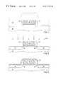
- FIG. 3is a cross-sectional view of a semiconductor topography, wherein a gate oxide is thermally grown across a semiconductor substrate;
- FIG. 4is a cross-sectional view of the semiconductor topography, wherein a polysilicon gate conductor is deposited across the gate oxide, subsequent to the step in FIG. 3;
- FIG. 5is a cross-sectional view of the semiconductor topography, wherein portions of the gate oxide and polysilicon gate conductor are removed to define a pair of opposed sidewall surfaces for the gate conductor, subsequent to the step in FIG. 4;
- FIG. 6is a cross-sectional view of the semiconductor topography, wherein an LDD implant which is self-aligned to the sidewall surfaces of the gate conductor is forwarded to the substrate, subsequent to the step in FIG. 5;
- FIG. 7is a cross-sectional view of the semiconductor topography, wherein nitride sidewall spacers are formed laterally adjacent to the gate conductor, subsequent to the step in FIG. 6;
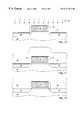
- FIG. 8is a cross-sectional view of the semiconductor topography, wherein a source/drain implant which is self-aligned to the exposed lateral edges of the nitride spacers is forwarded to the substrate, subsequent to the step in FIG. 7;
- FIG. 9is cross-sectional view of the semiconductor topography, wherein a refractory metal is deposited across exposed surfaces of the topography, subsequent to the step in FIG. 8;
- FIG. 10cross-sectional view of the semiconductor topography, wherein a metal salicide is formed upon the gate conductor and the source/drain regions of the substrate, subsequent to the step in FIG. 9;
- FIG. 11is a cross-sectional view of the semiconductor topography, wherein an interlevel dielectric is deposited across the exposed surfaces of the topography, subsequent to the step in FIG. 10;
- FIG. 12is a cross-sectional view of the semiconductor topography, wherein the upper surface of the interlevel dielectric is planarized, subsequent to the step in FIG. 11;
- FIG. 13is a cross-sectional view of the semiconductor topography, wherein a slightly misaligned contact opening is shown etched down to the gate conductor and partial nitride spacer, subsequent to the step in FIG. 12;
- FIG. 14is a cross-sectional view of the semiconductor topography, wherein a conductive contact is formed within the contact opening, subsequent to the step in FIG. 13 .
- FIG. 1illustrates an exemplary ICP reactor which may be used to deposit nitride from a high density plasma according to one embodiment of the present invention.
- the ICP reactorincludes a housing 2 mounted onto a top plate 6 .
- An induction coil 3is positioned within housing 2 about a vacuum chamber 5 which is contained within a quartz vessel 4 .
- vessel 4is hemispherically shaped to provide balanced coupling of RF into vacuum chamber 5 .
- An electrically conductive wafer support pedestal 7is arranged at the base of chamber 5 which includes a movable platen 9 for holding a semiconductor topography 8 .
- a vacuum systemmay be connected to a transfer region 14 for evacuating chamber 5 , and process gas may be furnished to the chamber through port 15 .
- the ICP reactoralso includes an RF generator subsystem having matching capacitors 11 which each have one terminal screwed into a copper bus bar 13 .
- Bus bar 13is mounted onto a dielectric block 12 which is attached to housing 10 .
- Induction coil 3is coupled to the RF matching network capacitors 11 , and bus bar 13 is connected to a low frequency RF source.
- FIG. 2depicts an ECR reactor which may be used for the deposition of nitride during processing of an integrated circuit according to another embodiment of the present invention.
- the ECR reactorincludes a housing 16 having a quartz window 17 , a gas inlet port 16 , and outlet ports 19 and 21 which are connected to a gas pump and a gas analyzer, respectively.
- a movable platen 25is disposed within the reactor near the base of housing 16 .
- a wafer comprising a semiconductor topographymay be positioned upon platen 25 such that topological features on the wafer protrude upward.
- a movable primary magnetic field 23 asurrounds housing 16 .
- Magnetic field 23 amay be used to move a plasma generated in the reactor toward platen 25 so that excite,d atoms within the plasma can be deposited upon the wafer.
- a secondary magnetic field 23 bis preferably disposed around housing 16 adjacent to platen 25 to control the flow of the generated plasma.
- a semiconductor substrate 20is provided which may comprise single crystalline silicon. Although not shown in the depicted cross-section of substrate 20 , dielectric isolation regions, such as trench isolation structures may be arranged spaced distances apart within the substrate for dielectrically isolating ensuing active areas.
- a gate dielectric 22comprising e.g., oxide may be thermally grown across substrate 20 by subjecting the substrate to thermal radiation 21 at a temperature of greater than about 700° C. while in an oxygen bearing ambient.
- a polysilicon gate conductor 24may be formed across gate dielectric 22 by using CVD of polysilicon from e.g., a silane source.
- FIG. 4depicts the removal of portions of gate dielectric 22 and polysilicon gate conductor 24 down to the surface of semiconductor substrate 20 , thereby defining a pair of opposed sidewall surfaces for gate conductor 24 .
- Removal of those portions of gate dielectric 22 and gate conductor 24may be achieved by using optical lithography to define a photoresist masking layer across those portions followed by e.g., a dry, plasma etch. Etch duration is chosen to terminate before substantial portions of substrate 20 are removed.
- an LDD implantmay then be forwarded to semiconductor substrate 20 .
- the LDD implantis aligned to the opposed sidewall surfaces of gate conductor 24 , and thereby leads to the formation of LDD areas 26 within regions of substrate 20 not masked by the gate conductor and exclusive of isolation regions.
- the LDD areas 26preferably contain a light concentration of dopants that are opposite in type to the dopants implanted within the bulk of substrate 20 .
- nitride 28is then CVD deposited to a thickness of approximately 300 ⁇ to 2000 ⁇ from a high density plasma source across exposed regions of substrate 20 and gate dielectric 24 .
- the high density plasma depositionmay be performed using the ICP reactor depicted in FIG. 1 .
- the semiconductor topographyis placed upon platen 9 in preparation for the nitride deposition.
- Gas within chamber 5is evacuated through transfer region 60 using a vacuum system.
- An inert gas, e.g., Armay be passed into chamber 5 through port 15 to establish a low pressure less than about 10 mTorr within the reactor chamber.
- Induction coil 18is powered by a low frequency (e.g., 450 KHz) RF generator which is connected to coil 18 via a low frequency matching network comprising capacitors 11 .
- the low frequency matching networkmay be tuned to couple low frequency RF energy into chamber 4 for the production of a high density plasma having approximately 10 11 ions/cm 3 .
- a process gas bearing a nitrogen-containing molecule, preferably N 2 , and a silicon-containing molecule, preferably SiH 4is passed into the plasma.
- a high frequency (e.g., 13.56 MHz) RF generatoris connected to platen 9 by an autotune high frequency matching network.
- the high frequency matching networkincludes an internal dc bias control that allows a regulated bias voltage to be achieved at wafer 8 . In response to the bias voltage, nitrogen and silicon radicals contained within the plasma become deposited upon the semiconductor topography where they react to form nitride.
- the ECR reactor shown in FIG. 2may be used to deposit nitride 28 .
- the semiconductor topographyPrior to the nitride deposition, the semiconductor topography is positioned upon platen 25 and the pressure within the reactor is decreased to below approximately 10 millitorr while the temperature is increased to between approximately 100° C. and 400° C.
- a gas comprising a nitrogen-containing molecule, preferably N 2is then injected into the chamber through inlet port 18 .
- a microwave di chargeis introduced into the reactor via quartz window 17 , and a plasma is formed in the vicinity of the primary magnetic field coil 23 a where an ECR condition is established.
- the primary magnetic field coil 23 amay be moved toward platen 25 so as to compel the plasma toward the semiconductor topography.
- Silanemay then be injected into the excited plasma or the afterglow thereof in order to produce ions and highly reactive radicals from the silane and the N 2 .
- the ECR magnetic fieldis applied to the plasma at a relatively high frequency greater than approximately 1 GHz such that the plasma comprises more than approximately 10 11 ions/cm 3 .
- controlis exerted over the plasma such that the energy and flux of the ions and electrons are regulated.
- the nitrogen and silicon radicalsare deposited upon the surface of the semiconductor topography where they react to form a substantially stoichiometric nitride which is free of contaminants, such as hydrogen and oxygen.
- portions of nitride 28may be removed to form nitride sidewall spacers 30 directly adjacent to the opposed sidewall surfaces of gate conductor 24 .
- the removal of nitride 28may be accomplished using an anisotropic etch in which ion bombardment of the nitride occurs at a faster rate in a vertical direction than in a horizontal direction.
- the anisotropic etchmay be performed until a pre-defined lateral thickness of nitride 28 remains exclusively adjacent to the sidewall surfaces of gate conductor 24 .
- a heavy concentration source/drain (S/D) implantis then self-aligned to the exposed lateral surfaces of nitride spacers 30 .
- dopantsare also forwarded into gate conductor 24 such that the conductivity of the gate conductor is increased.
- the dopants used for the S/D implantare of the same type as those used for the LDD implant.
- a PMOSFET transistoris being formed, ion implantation of p-type species is performed.
- n-type speciesare implanted into substrate 20 .
- Some commonly used n-type dopantsare arsenic or phosphorus, and some commonly used p-type dopants are boron or boron difluoride.
- the resulting transistorhas graded junctions in which dopant concentration increases laterally in a direction away from gate conductor 24 . In other words, source/drain regions 32 are formed within semiconductor substrate 20 which are more heavily concentrated with dopants than LDD areas 26 .
- a refractory metal 28e.g., titanium or cobalt, may be formed across exposed surfaces of gate conductor 24 , nitride spacers 28 , and substrate 20 .
- Refractory metal 28may be sputter deposited from a metal target or MOCVD (“metal organic” CVD) deposited from a source comprising a volatile metal organic compound.
- MOCVDmetal organic
- a metal salicide 36self-aligned silicide
- Metal salicide 36may be formed exclusively upon exposed regions of substrate 20 and gate conductor 24 .
- Metal salicide 36may be formed by exposing refractory metal 28 to a form of radiation 34 capable of increasing the temperature of the refractory metal. Radiation 34 may be thermal radiation provided from a heated furnace.
- radiation 34may be radiant light supplied from e.g., an arc lamp or a tungsten-halogen lamp using a technique known as rapid thermal processing (“RTP”).
- RTPrapid thermal processing
- the use of RTP to heat refractory metal 34may reduce the amount of unwanted dopant diffusion into the semiconductor topography as compared to using a high temperature furnace. Raising the temperature of refractory metal 34 serves to initiate reaction between metal atoms and silicon atoms of polysilicon gate conductor 24 and substrate 20 . Any unreacted refractory metal which remains may be etched away using e.g., a wet etch highly selective to the metal.
- the resulting metal salicide 36has a relatively low resistivity and serves as a self-aligned contact region across source/drain regions 32 and gate conductor 24 .
- FIG. 10depicts an interlevel dielectric 38 being CVD deposited across exposed surfaces of metal salicide 36 and nitride spacers 30 .
- Interlevel dielectric 38may comprise, for example, a single oxide layer or an oxynitride layer combined with an overlying oxide layer.
- the upper surface of interlevel dielectric 38may be planarized using e.g., chemical-mechanical polishing.
- FIG. 12depicts the formation of a contact opening 40 through interlevel dielectric 38 such that the metal salicide 36 disposed across gate conductor 24 is exposed.
- a portion of interlevel dielectric 38may be etched away to form contact opening 40 using e.g., an etch technique which is highly selective to the interlevel dielectric 38 material.
- the photoresist masking layer used to define the portion of interlevel dielectric 38 to be etchedhas been mis-aligned such that contact opening 40 is shifted leftward from its targeted location. Although not intentional, opening 40 may unfortunately be slightly mis-aligned to allow a portion of spacer 30 to be exposed adjacent metal salicide 35 . Fortunately, since sidewall spacers 30 are composed of nitride, the etchant used to remove oxide-based interlevel dielectric 38 does not substantially attack the nitride-based spacers.
- FIG. 13depicts the formation of a conductive contact 42 within the contact opening.
- a conductive material 44such as tungsten or titanium may be sputter deposited or MOCVD deposited into the contact opening and across interlevel dielectric 38 .
- Conductive material 44may then be removed down to a level commensurate with the upper surface of interlevel dielectric 38 such that the upper surface of contact 42 is even with that of the interlevel dielectric.
- a local interconnectcomprising e.g., polysilicon may subsequently be formed across interlevel dielectric 38 such that it is coupled to contact 42 .
- conductive material 44may be allowed to remain above interlevel dielectric 38 to serve both as a contact and a local interconnect.
- nitride spacers 30advantageously prohibits contact 42 from extending into the region directly adjacent to the sidewall surfaces of gate conductor 24 , thereby reducing the possibility of a conductive path forming between gate conductor 24 and adjacent S/D regions 32 .
Landscapes
- Engineering & Computer Science (AREA)
- Chemical & Material Sciences (AREA)
- Condensed Matter Physics & Semiconductors (AREA)
- Inorganic Chemistry (AREA)
- Physics & Mathematics (AREA)
- General Chemical & Material Sciences (AREA)
- Chemical Kinetics & Catalysis (AREA)
- General Physics & Mathematics (AREA)
- Manufacturing & Machinery (AREA)
- Computer Hardware Design (AREA)
- Microelectronics & Electronic Packaging (AREA)
- Power Engineering (AREA)
- Insulated Gate Type Field-Effect Transistor (AREA)
Abstract
Description
Claims (13)
Priority Applications (1)
| Application Number | Priority Date | Filing Date | Title |
|---|---|---|---|
| US09/048,192US6171917B1 (en) | 1998-03-25 | 1998-03-25 | Transistor sidewall spacers composed of silicon nitride CVD deposited from a high density plasma source |
Applications Claiming Priority (1)
| Application Number | Priority Date | Filing Date | Title |
|---|---|---|---|
| US09/048,192US6171917B1 (en) | 1998-03-25 | 1998-03-25 | Transistor sidewall spacers composed of silicon nitride CVD deposited from a high density plasma source |
Publications (1)
| Publication Number | Publication Date |
|---|---|
| US6171917B1true US6171917B1 (en) | 2001-01-09 |
Family
ID=21953202
Family Applications (1)
| Application Number | Title | Priority Date | Filing Date |
|---|---|---|---|
| US09/048,192Expired - LifetimeUS6171917B1 (en) | 1998-03-25 | 1998-03-25 | Transistor sidewall spacers composed of silicon nitride CVD deposited from a high density plasma source |
Country Status (1)
| Country | Link |
|---|---|
| US (1) | US6171917B1 (en) |
Cited By (16)
| Publication number | Priority date | Publication date | Assignee | Title |
|---|---|---|---|---|
| US6388334B1 (en)* | 1999-07-27 | 2002-05-14 | Advanced Micro Devices, Inc. | System and method for circuit rebuilding via backside access |
| US6486038B1 (en) | 2001-03-12 | 2002-11-26 | Advanced Micro Devices | Method for and device having STI using partial etch trench bottom liner |
| US20030022429A1 (en)* | 2001-07-26 | 2003-01-30 | Mitsubishi Denki Kabushiki Kaisha | Electrode structure and method of fabricating the same |
| US6521510B1 (en) | 2001-03-23 | 2003-02-18 | Advanced Micro Devices, Inc. | Method for shallow trench isolation with removal of strained island edges |
| US6524929B1 (en) | 2001-02-26 | 2003-02-25 | Advanced Micro Devices, Inc. | Method for shallow trench isolation using passivation material for trench bottom liner |
| US6531394B1 (en)* | 2000-07-21 | 2003-03-11 | Hyundai Electronics Industries Co., Ltd. | Method for forming gate electrode of semiconductor device |
| US6534379B1 (en) | 2001-03-26 | 2003-03-18 | Advanced Micro Devices, Inc. | Linerless shallow trench isolation method |
| US20030194510A1 (en)* | 2002-04-16 | 2003-10-16 | Applied Materials, Inc. | Methods used in fabricating gates in integrated circuit device structures |
| US6638848B1 (en)* | 1999-03-03 | 2003-10-28 | Sony Corporation | Method of etching insulating film and method of forming interconnection layer |
| RU2216818C1 (en)* | 2003-01-28 | 2003-11-20 | Общество с ограниченной ответственностью "ЭпиЛаб" | Electron cyclotron resonance -plasma source to process semiconductor structures, method to process semiconductor structures, process of manufacture of semiconductor devices and integrated circuits ( variants ), semiconductor device or integrated circuit ( variants ) |
| US20070269992A1 (en)* | 2006-05-19 | 2007-11-22 | International Business Machines Corporation | Compressive nitride film and method of manufacturing thereof |
| US20090163041A1 (en)* | 2007-12-21 | 2009-06-25 | Applied Materials, Inc. | Low wet etch rate silicon nitride film |
| US9018108B2 (en) | 2013-01-25 | 2015-04-28 | Applied Materials, Inc. | Low shrinkage dielectric films |
| US9679746B2 (en)* | 2015-10-28 | 2017-06-13 | Taiwan Semiconductor Manufacturing Co., Ltd. | Ion implantation tool and ion implantation method |
| WO2017160649A1 (en)* | 2016-03-13 | 2017-09-21 | Applied Materials, Inc. | Methods and apparatus for selective dry etch |
| CN113130386A (en)* | 2020-01-15 | 2021-07-16 | 台湾积体电路制造股份有限公司 | Integrated circuit structure and forming method thereof |
Citations (16)
| Publication number | Priority date | Publication date | Assignee | Title |
|---|---|---|---|---|
| US5089865A (en)* | 1989-01-07 | 1992-02-18 | Mitsubishi Denki Kabushiki Kaisha | Mis semiconductor device |
| US5324974A (en) | 1990-09-04 | 1994-06-28 | Industrial Technology Research Institute | Nitride capped MOSFET for integrated circuits |
| US5334870A (en) | 1992-04-17 | 1994-08-02 | Nippondenso Co. Ltd. | Complementary MIS transistor and a fabrication process thereof |
| US5346578A (en) | 1992-11-04 | 1994-09-13 | Novellus Systems, Inc. | Induction plasma source |
| US5621241A (en) | 1994-08-17 | 1997-04-15 | Texas Instruments Incorporated | Enhancement in throughput and planarity during CMP using a dielectric stack containing HDP-SiO2 films |
| US5641480A (en) | 1994-12-08 | 1997-06-24 | Lever Brothers Company, Division Of Conopco, Inc. | Hair care compositions comprising heteroatom containing alkyl aldonamide compounds |
| US5641546A (en)* | 1996-05-06 | 1997-06-24 | Hughes Aircraft Company | Passivation of electronic modules using high density plasmas |
| US5648284A (en) | 1991-09-05 | 1997-07-15 | Mitsubishi Denki Kabushiki Kaisha | Field effect transistor including silicon oxide film and nitrided oxide film as gate insulator film and manufacturing method thereof |
| US5719425A (en) | 1996-01-31 | 1998-02-17 | Micron Technology, Inc. | Multiple implant lightly doped drain (MILDD) field effect transistor |
| US5780896A (en) | 1995-12-21 | 1998-07-14 | Nec Corporation | Semiconductor device having shallow impurity region without short-circuit between gate electrode and source and drain regions and process of fabrication thereof |
| US5818092A (en) | 1996-02-15 | 1998-10-06 | Intel Corporation | Polycide film |
| US5847428A (en) | 1996-12-06 | 1998-12-08 | Advanced Micro Devices, Inc. | Integrated circuit gate conductor which uses layered spacers to produce a graded junction |
| US5858848A (en)* | 1997-10-24 | 1999-01-12 | Advanced Micro Devices, Inc. | Semiconductor fabrication employing self-aligned sidewall spacers laterally adjacent to a transistor gate |
| US5895955A (en) | 1997-01-10 | 1999-04-20 | Advanced Micro Devices, Inc. | MOS transistor employing a removable, dual layer etch stop to protect implant regions from sidewall spacer overetch |
| US5905293A (en) | 1997-05-05 | 1999-05-18 | Vanguard International Semiconductor Corporation | LDD spacers in MOS devices with double spacers |
| US5937315A (en) | 1997-11-07 | 1999-08-10 | Advanced Micro Devices, Inc. | Self-aligned silicide gate technology for advanced submicron MOS devices |
- 1998
- 1998-03-25USUS09/048,192patent/US6171917B1/ennot_activeExpired - Lifetime
Patent Citations (17)
| Publication number | Priority date | Publication date | Assignee | Title |
|---|---|---|---|---|
| US5089865A (en)* | 1989-01-07 | 1992-02-18 | Mitsubishi Denki Kabushiki Kaisha | Mis semiconductor device |
| US5324974A (en) | 1990-09-04 | 1994-06-28 | Industrial Technology Research Institute | Nitride capped MOSFET for integrated circuits |
| US5648284A (en) | 1991-09-05 | 1997-07-15 | Mitsubishi Denki Kabushiki Kaisha | Field effect transistor including silicon oxide film and nitrided oxide film as gate insulator film and manufacturing method thereof |
| US5334870A (en) | 1992-04-17 | 1994-08-02 | Nippondenso Co. Ltd. | Complementary MIS transistor and a fabrication process thereof |
| US5405480A (en)* | 1992-11-04 | 1995-04-11 | Novellus Systems, Inc. | Induction plasma source |
| US5346578A (en) | 1992-11-04 | 1994-09-13 | Novellus Systems, Inc. | Induction plasma source |
| US5621241A (en) | 1994-08-17 | 1997-04-15 | Texas Instruments Incorporated | Enhancement in throughput and planarity during CMP using a dielectric stack containing HDP-SiO2 films |
| US5641480A (en) | 1994-12-08 | 1997-06-24 | Lever Brothers Company, Division Of Conopco, Inc. | Hair care compositions comprising heteroatom containing alkyl aldonamide compounds |
| US5780896A (en) | 1995-12-21 | 1998-07-14 | Nec Corporation | Semiconductor device having shallow impurity region without short-circuit between gate electrode and source and drain regions and process of fabrication thereof |
| US5719425A (en) | 1996-01-31 | 1998-02-17 | Micron Technology, Inc. | Multiple implant lightly doped drain (MILDD) field effect transistor |
| US5818092A (en) | 1996-02-15 | 1998-10-06 | Intel Corporation | Polycide film |
| US5641546A (en)* | 1996-05-06 | 1997-06-24 | Hughes Aircraft Company | Passivation of electronic modules using high density plasmas |
| US5847428A (en) | 1996-12-06 | 1998-12-08 | Advanced Micro Devices, Inc. | Integrated circuit gate conductor which uses layered spacers to produce a graded junction |
| US5895955A (en) | 1997-01-10 | 1999-04-20 | Advanced Micro Devices, Inc. | MOS transistor employing a removable, dual layer etch stop to protect implant regions from sidewall spacer overetch |
| US5905293A (en) | 1997-05-05 | 1999-05-18 | Vanguard International Semiconductor Corporation | LDD spacers in MOS devices with double spacers |
| US5858848A (en)* | 1997-10-24 | 1999-01-12 | Advanced Micro Devices, Inc. | Semiconductor fabrication employing self-aligned sidewall spacers laterally adjacent to a transistor gate |
| US5937315A (en) | 1997-11-07 | 1999-08-10 | Advanced Micro Devices, Inc. | Self-aligned silicide gate technology for advanced submicron MOS devices |
Non-Patent Citations (2)
| Title |
|---|
| Tuszewski, et al, "Characterization of a Low Frequency Inductively Coupled Plasma Source," Novelius Technical Paper, Journal of Vacuum Science & Technology, Rev. A, vol. 14, Issue No. 3, May 1996 pp. 1096-1101. |
| Wolf, "Silicon Processing For the VLSI Era, vol. 3: the Submicron MOSFET," Lattice Press, Sunset Beach, California, pp. 660-661, No Month. |
Cited By (27)
| Publication number | Priority date | Publication date | Assignee | Title |
|---|---|---|---|---|
| US6638848B1 (en)* | 1999-03-03 | 2003-10-28 | Sony Corporation | Method of etching insulating film and method of forming interconnection layer |
| US6388334B1 (en)* | 1999-07-27 | 2002-05-14 | Advanced Micro Devices, Inc. | System and method for circuit rebuilding via backside access |
| US6531394B1 (en)* | 2000-07-21 | 2003-03-11 | Hyundai Electronics Industries Co., Ltd. | Method for forming gate electrode of semiconductor device |
| US6524929B1 (en) | 2001-02-26 | 2003-02-25 | Advanced Micro Devices, Inc. | Method for shallow trench isolation using passivation material for trench bottom liner |
| US6747333B1 (en) | 2001-02-26 | 2004-06-08 | Advanced Micro Devices, Inc. | Method and apparatus for STI using passivation material for trench bottom liner |
| US6486038B1 (en) | 2001-03-12 | 2002-11-26 | Advanced Micro Devices | Method for and device having STI using partial etch trench bottom liner |
| US6521510B1 (en) | 2001-03-23 | 2003-02-18 | Advanced Micro Devices, Inc. | Method for shallow trench isolation with removal of strained island edges |
| US6534379B1 (en) | 2001-03-26 | 2003-03-18 | Advanced Micro Devices, Inc. | Linerless shallow trench isolation method |
| US20030022429A1 (en)* | 2001-07-26 | 2003-01-30 | Mitsubishi Denki Kabushiki Kaisha | Electrode structure and method of fabricating the same |
| US6784546B2 (en)* | 2001-07-26 | 2004-08-31 | Renesas Technology Corp. | Electrode structure and method of fabricating the same |
| US20030194510A1 (en)* | 2002-04-16 | 2003-10-16 | Applied Materials, Inc. | Methods used in fabricating gates in integrated circuit device structures |
| RU2216818C1 (en)* | 2003-01-28 | 2003-11-20 | Общество с ограниченной ответственностью "ЭпиЛаб" | Electron cyclotron resonance -plasma source to process semiconductor structures, method to process semiconductor structures, process of manufacture of semiconductor devices and integrated circuits ( variants ), semiconductor device or integrated circuit ( variants ) |
| US20070269992A1 (en)* | 2006-05-19 | 2007-11-22 | International Business Machines Corporation | Compressive nitride film and method of manufacturing thereof |
| WO2007136907A3 (en)* | 2006-05-19 | 2008-01-10 | Ibm | Compressive nitride film and method of manufacturing thereof |
| US7514370B2 (en) | 2006-05-19 | 2009-04-07 | International Business Machines Corporation | Compressive nitride film and method of manufacturing thereof |
| TWI426560B (en)* | 2006-05-19 | 2014-02-11 | Ibm | Compressed nitride film and method of producing the same |
| US20090163041A1 (en)* | 2007-12-21 | 2009-06-25 | Applied Materials, Inc. | Low wet etch rate silicon nitride film |
| WO2009085974A3 (en)* | 2007-12-21 | 2009-09-24 | Applied Materials, Inc. | Low wet etch rate silicon nitride film |
| US7678715B2 (en) | 2007-12-21 | 2010-03-16 | Applied Materials, Inc. | Low wet etch rate silicon nitride film |
| US9018108B2 (en) | 2013-01-25 | 2015-04-28 | Applied Materials, Inc. | Low shrinkage dielectric films |
| US9679746B2 (en)* | 2015-10-28 | 2017-06-13 | Taiwan Semiconductor Manufacturing Co., Ltd. | Ion implantation tool and ion implantation method |
| TWI701698B (en)* | 2015-10-28 | 2020-08-11 | 台灣積體電路製造股份有限公司 | Ion implantation tool and method |
| WO2017160649A1 (en)* | 2016-03-13 | 2017-09-21 | Applied Materials, Inc. | Methods and apparatus for selective dry etch |
| CN108778739A (en)* | 2016-03-13 | 2018-11-09 | 应用材料公司 | Method and apparatus for selective dry-etching |
| US10134581B2 (en) | 2016-03-13 | 2018-11-20 | Applied Materials, Inc. | Methods and apparatus for selective dry etch |
| CN108778739B (en)* | 2016-03-13 | 2021-07-16 | 应用材料公司 | Method and apparatus for selective dry etching |
| CN113130386A (en)* | 2020-01-15 | 2021-07-16 | 台湾积体电路制造股份有限公司 | Integrated circuit structure and forming method thereof |
Similar Documents
| Publication | Publication Date | Title |
|---|---|---|
| US8268682B2 (en) | Method for manufacturing a semiconductor integrated circuit device | |
| US6432830B1 (en) | Semiconductor fabrication process | |
| KR100931765B1 (en) | Oxide Etching Using NH3-NF3 Chemicals | |
| US6171917B1 (en) | Transistor sidewall spacers composed of silicon nitride CVD deposited from a high density plasma source | |
| US6081010A (en) | MOS semiconductor device with self-aligned punchthrough stops and method of fabrication | |
| US6713392B1 (en) | Nitrogen oxide plasma treatment for reduced nickel silicide bridging | |
| US5770508A (en) | Method of forming lightly doped drains in metalic oxide semiconductor components | |
| US11972951B2 (en) | Selective formation of titanium silicide and titanium nitride by hydrogen gas control | |
| US5585295A (en) | Method for forming inverse-T gate lightly-doped drain (ITLDD) device | |
| KR100281307B1 (en) | Method for manufacturing semiconductor device using selective epitaxial growth | |
| US5858848A (en) | Semiconductor fabrication employing self-aligned sidewall spacers laterally adjacent to a transistor gate | |
| US8481389B2 (en) | Method of removing high-K dielectric layer on sidewalls of gate structure | |
| US8836048B2 (en) | Field effect transistor device having a hybrid metal gate stack | |
| WO2016133673A1 (en) | Gate electrode material residual removal process | |
| KR20230044033A (en) | Methods for depositing dielectric material | |
| US20050009283A1 (en) | Method for removal of a spacer | |
| US7341903B2 (en) | Method of forming a field effect transistor having a stressed channel region | |
| US5874343A (en) | CMOS integrated circuit and method for forming source/drain areas prior to forming lightly doped drains to optimize the thermal diffusivity thereof | |
| US6465349B1 (en) | Nitrogen-plasma treatment for reduced nickel silicide bridging | |
| US7381602B2 (en) | Method of forming a field effect transistor comprising a stressed channel region | |
| JPH10144625A (en) | Method for manufacturing semiconductor device | |
| JP2674585B2 (en) | Method for manufacturing semiconductor device | |
| US6548403B1 (en) | Silicon oxide liner for reduced nickel silicide bridging | |
| KR100499755B1 (en) | Method of fabricating deep sub-micron cmos source/drain with mdd and selective cvd silicide | |
| US20070254492A1 (en) | Technique for forming a silicon nitride layer having high intrinsic compressive stress |
Legal Events
| Date | Code | Title | Description |
|---|---|---|---|
| AS | Assignment | Owner name:ADVANCED MICRO DEVICES, INC., CALIFORNIA Free format text:ASSIGNMENT OF ASSIGNORS INTEREST;ASSIGNORS:SUN, SEY-PING;SPIKES, THOMAS E.;HAUSE, FRED N.;REEL/FRAME:009076/0624 Effective date:19980311 | |
| STCF | Information on status: patent grant | Free format text:PATENTED CASE | |
| FPAY | Fee payment | Year of fee payment:4 | |
| FEPP | Fee payment procedure | Free format text:PAYER NUMBER DE-ASSIGNED (ORIGINAL EVENT CODE: RMPN); ENTITY STATUS OF PATENT OWNER: LARGE ENTITY Free format text:PAYOR NUMBER ASSIGNED (ORIGINAL EVENT CODE: ASPN); ENTITY STATUS OF PATENT OWNER: LARGE ENTITY | |
| FPAY | Fee payment | Year of fee payment:8 | |
| AS | Assignment | Owner name:GLOBALFOUNDRIES INC., CAYMAN ISLANDS Free format text:AFFIRMATION OF PATENT ASSIGNMENT;ASSIGNOR:ADVANCED MICRO DEVICES, INC.;REEL/FRAME:023119/0083 Effective date:20090630 Owner name:GLOBALFOUNDRIES INC., CAYMAN ISLANDS Free format text:AFFIRMATION OF PATENT ASSIGNMENT;ASSIGNOR:ADVANCED MICRO DEVICES, INC.;REEL/FRAME:023120/0426 Effective date:20090630 Owner name:GLOBALFOUNDRIES INC.,CAYMAN ISLANDS Free format text:AFFIRMATION OF PATENT ASSIGNMENT;ASSIGNOR:ADVANCED MICRO DEVICES, INC.;REEL/FRAME:023120/0426 Effective date:20090630 | |
| FPAY | Fee payment | Year of fee payment:12 | |
| AS | Assignment | Owner name:GLOBALFOUNDRIES U.S. INC., NEW YORK Free format text:RELEASE BY SECURED PARTY;ASSIGNOR:WILMINGTON TRUST, NATIONAL ASSOCIATION;REEL/FRAME:056987/0001 Effective date:20201117 |