US6170428B1 - Symmetric tunable inductively coupled HDP-CVD reactor - Google Patents
Symmetric tunable inductively coupled HDP-CVD reactorDownload PDFInfo
- Publication number
- US6170428B1 US6170428B1US08/679,927US67992796AUS6170428B1US 6170428 B1US6170428 B1US 6170428B1US 67992796 AUS67992796 AUS 67992796AUS 6170428 B1US6170428 B1US 6170428B1
- Authority
- US
- United States
- Prior art keywords
- substrate
- chamber
- lid
- gas
- matching network
- Prior art date
- Legal status (The legal status is an assumption and is not a legal conclusion. Google has not performed a legal analysis and makes no representation as to the accuracy of the status listed.)
- Expired - Lifetime
Links
- 239000007789gasSubstances0.000claimsabstractdescription93
- 238000004140cleaningMethods0.000claimsabstractdescription39
- 230000008021depositionEffects0.000claimsabstractdescription32
- 238000009826distributionMethods0.000claimsabstractdescription16
- 230000009977dual effectEffects0.000claimsabstractdescription13
- 239000000919ceramicSubstances0.000claimsabstractdescription4
- 239000000758substrateSubstances0.000claimsdescription69
- 238000000034methodMethods0.000claimsdescription22
- 239000000463materialSubstances0.000claimsdescription12
- 230000008569processEffects0.000claimsdescription11
- 238000005086pumpingMethods0.000claimsdescription7
- 230000008859changeEffects0.000claimsdescription5
- XKRFYHLGVUSROY-UHFFFAOYSA-NArgonChemical compound[Ar]XKRFYHLGVUSROY-UHFFFAOYSA-N0.000claimsdescription4
- 239000004065semiconductorSubstances0.000claimsdescription4
- TWNQGVIAIRXVLR-UHFFFAOYSA-Noxo(oxoalumanyloxy)alumaneChemical compoundO=[Al]O[Al]=OTWNQGVIAIRXVLR-UHFFFAOYSA-N0.000claimsdescription3
- 229910020323ClF3Inorganic materials0.000claimsdescription2
- 229910052786argonInorganic materials0.000claimsdescription2
- 230000008878couplingEffects0.000claimsdescription2
- 238000010168coupling processMethods0.000claimsdescription2
- 238000005859coupling reactionMethods0.000claimsdescription2
- 239000003989dielectric materialSubstances0.000claimsdescription2
- JOHWNGGYGAVMGU-UHFFFAOYSA-NtrifluorochlorineChemical compoundFCl(F)FJOHWNGGYGAVMGU-UHFFFAOYSA-N0.000claimsdescription2
- 125000001153fluoro groupChemical groupF*0.000claims2
- PMHQVHHXPFUNSP-UHFFFAOYSA-Mcopper(1+);methylsulfanylmethane;bromideChemical compoundBr[Cu].CSCPMHQVHHXPFUNSP-UHFFFAOYSA-M0.000claims1
- 238000005530etchingMethods0.000claims1
- 238000000151depositionMethods0.000abstractdescription31
- 235000012431wafersNutrition0.000abstractdescription23
- VYPSYNLAJGMNEJ-UHFFFAOYSA-NSilicium dioxideChemical compoundO=[Si]=OVYPSYNLAJGMNEJ-UHFFFAOYSA-N0.000abstractdescription12
- 238000001816coolingMethods0.000abstractdescription6
- 239000000377silicon dioxideSubstances0.000abstractdescription6
- 239000001307heliumSubstances0.000abstractdescription5
- 229910052734heliumInorganic materials0.000abstractdescription5
- SWQJXJOGLNCZEY-UHFFFAOYSA-Nhelium atomChemical compound[He]SWQJXJOGLNCZEY-UHFFFAOYSA-N0.000abstractdescription5
- 239000002245particleSubstances0.000abstractdescription5
- 235000012239silicon dioxideNutrition0.000abstractdescription5
- YCKRFDGAMUMZLT-UHFFFAOYSA-NFluorine atomChemical compound[F]YCKRFDGAMUMZLT-UHFFFAOYSA-N0.000abstractdescription4
- 229910052731fluorineInorganic materials0.000abstractdescription4
- 239000011737fluorineSubstances0.000abstractdescription4
- 238000010276constructionMethods0.000abstractdescription3
- 229910000838Al alloyInorganic materials0.000abstractdescription2
- 229910002110ceramic alloyInorganic materials0.000abstractdescription2
- 238000009616inductively coupled plasmaMethods0.000abstractdescription2
- 238000004544sputter depositionMethods0.000abstractdescription2
- 210000002381plasmaAnatomy0.000description38
- 239000010408filmSubstances0.000description14
- 150000002500ionsChemical class0.000description9
- 238000005229chemical vapour depositionMethods0.000description8
- 239000000376reactantSubstances0.000description6
- 238000000429assemblyMethods0.000description5
- 230000000712assemblyEffects0.000description5
- 238000006243chemical reactionMethods0.000description5
- 238000004519manufacturing processMethods0.000description5
- 230000008901benefitEffects0.000description4
- 239000003990capacitorSubstances0.000description4
- 238000002347injectionMethods0.000description3
- 239000007924injectionSubstances0.000description3
- 230000001590oxidative effectEffects0.000description3
- 239000011521glassSubstances0.000description2
- 230000001965increasing effectEffects0.000description2
- 230000007935neutral effectEffects0.000description2
- 239000000523sampleSubstances0.000description2
- 238000004804windingMethods0.000description2
- PIGFYZPCRLYGLF-UHFFFAOYSA-NAluminum nitrideChemical compound[Al]#NPIGFYZPCRLYGLF-UHFFFAOYSA-N0.000description1
- 229910052581Si3N4Inorganic materials0.000description1
- 229910004016SiF2Inorganic materials0.000description1
- 229910004014SiF4Inorganic materials0.000description1
- 229910020489SiO3Inorganic materials0.000description1
- 230000009471actionEffects0.000description1
- 229910052782aluminiumInorganic materials0.000description1
- XAGFODPZIPBFFR-UHFFFAOYSA-NaluminiumChemical compound[Al]XAGFODPZIPBFFR-UHFFFAOYSA-N0.000description1
- QVGXLLKOCUKJST-UHFFFAOYSA-Natomic oxygenChemical compound[O]QVGXLLKOCUKJST-UHFFFAOYSA-N0.000description1
- 230000015572biosynthetic processEffects0.000description1
- 210000004027cellAnatomy0.000description1
- 229910052681coesiteInorganic materials0.000description1
- 239000004020conductorSubstances0.000description1
- 238000011109contaminationMethods0.000description1
- 229910052906cristobaliteInorganic materials0.000description1
- 230000003247decreasing effectEffects0.000description1
- 238000005137deposition processMethods0.000description1
- 238000010586diagramMethods0.000description1
- MGNHOGAVECORPT-UHFFFAOYSA-NdifluorosiliconChemical compoundF[Si]FMGNHOGAVECORPT-UHFFFAOYSA-N0.000description1
- 230000008846dynamic interplayEffects0.000description1
- 230000005284excitationEffects0.000description1
- 230000005281excited stateEffects0.000description1
- 238000010438heat treatmentMethods0.000description1
- 230000001939inductive effectEffects0.000description1
- 239000012212insulatorSubstances0.000description1
- 230000010354integrationEffects0.000description1
- 238000010849ion bombardmentMethods0.000description1
- 238000002955isolationMethods0.000description1
- 239000007788liquidSubstances0.000description1
- 230000005291magnetic effectEffects0.000description1
- 229910052751metalInorganic materials0.000description1
- 239000002184metalSubstances0.000description1
- 239000000203mixtureSubstances0.000description1
- NJPPVKZQTLUDBO-UHFFFAOYSA-NnovaluronChemical compoundC1=C(Cl)C(OC(F)(F)C(OC(F)(F)F)F)=CC=C1NC(=O)NC(=O)C1=C(F)C=CC=C1FNJPPVKZQTLUDBO-UHFFFAOYSA-N0.000description1
- 230000008520organizationEffects0.000description1
- 239000007800oxidant agentSubstances0.000description1
- 239000001301oxygenSubstances0.000description1
- 229910052760oxygenInorganic materials0.000description1
- 230000000737periodic effectEffects0.000description1
- 210000004180plasmocyteAnatomy0.000description1
- 229910021420polycrystalline siliconInorganic materials0.000description1
- 229920005591polysiliconPolymers0.000description1
- HQVNEWCFYHHQES-UHFFFAOYSA-Nsilicon nitrideChemical compoundN12[Si]34N5[Si]62N3[Si]51N64HQVNEWCFYHHQES-UHFFFAOYSA-N0.000description1
- ABTOQLMXBSRXSM-UHFFFAOYSA-Nsilicon tetrafluorideChemical compoundF[Si](F)(F)FABTOQLMXBSRXSM-UHFFFAOYSA-N0.000description1
- 229910052682stishoviteInorganic materials0.000description1
- 239000000126substanceSubstances0.000description1
- 239000002887superconductorSubstances0.000description1
- 239000010409thin filmSubstances0.000description1
- 229910052905tridymiteInorganic materials0.000description1
- WFKWXMTUELFFGS-UHFFFAOYSA-NtungstenChemical compound[W]WFKWXMTUELFFGS-UHFFFAOYSA-N0.000description1
- 229910052721tungstenInorganic materials0.000description1
- 239000010937tungstenSubstances0.000description1
- 238000001771vacuum depositionMethods0.000description1
Images


Classifications
- H—ELECTRICITY
- H01—ELECTRIC ELEMENTS
- H01L—SEMICONDUCTOR DEVICES NOT COVERED BY CLASS H10
- H01L21/00—Processes or apparatus adapted for the manufacture or treatment of semiconductor or solid state devices or of parts thereof
- H01L21/02—Manufacture or treatment of semiconductor devices or of parts thereof
- H01L21/04—Manufacture or treatment of semiconductor devices or of parts thereof the devices having potential barriers, e.g. a PN junction, depletion layer or carrier concentration layer
- H01L21/18—Manufacture or treatment of semiconductor devices or of parts thereof the devices having potential barriers, e.g. a PN junction, depletion layer or carrier concentration layer the devices having semiconductor bodies comprising elements of Group IV of the Periodic Table or AIIIBV compounds with or without impurities, e.g. doping materials
- H01L21/20—Deposition of semiconductor materials on a substrate, e.g. epitaxial growth solid phase epitaxy
- H—ELECTRICITY
- H01—ELECTRIC ELEMENTS
- H01J—ELECTRIC DISCHARGE TUBES OR DISCHARGE LAMPS
- H01J37/00—Discharge tubes with provision for introducing objects or material to be exposed to the discharge, e.g. for the purpose of examination or processing thereof
- H01J37/32—Gas-filled discharge tubes
- H01J37/32431—Constructional details of the reactor
- H01J37/3244—Gas supply means
- H01J37/32449—Gas control, e.g. control of the gas flow
- C—CHEMISTRY; METALLURGY
- C23—COATING METALLIC MATERIAL; COATING MATERIAL WITH METALLIC MATERIAL; CHEMICAL SURFACE TREATMENT; DIFFUSION TREATMENT OF METALLIC MATERIAL; COATING BY VACUUM EVAPORATION, BY SPUTTERING, BY ION IMPLANTATION OR BY CHEMICAL VAPOUR DEPOSITION, IN GENERAL; INHIBITING CORROSION OF METALLIC MATERIAL OR INCRUSTATION IN GENERAL
- C23C—COATING METALLIC MATERIAL; COATING MATERIAL WITH METALLIC MATERIAL; SURFACE TREATMENT OF METALLIC MATERIAL BY DIFFUSION INTO THE SURFACE, BY CHEMICAL CONVERSION OR SUBSTITUTION; COATING BY VACUUM EVAPORATION, BY SPUTTERING, BY ION IMPLANTATION OR BY CHEMICAL VAPOUR DEPOSITION, IN GENERAL
- C23C16/00—Chemical coating by decomposition of gaseous compounds, without leaving reaction products of surface material in the coating, i.e. chemical vapour deposition [CVD] processes
- C23C16/44—Chemical coating by decomposition of gaseous compounds, without leaving reaction products of surface material in the coating, i.e. chemical vapour deposition [CVD] processes characterised by the method of coating
- C23C16/50—Chemical coating by decomposition of gaseous compounds, without leaving reaction products of surface material in the coating, i.e. chemical vapour deposition [CVD] processes characterised by the method of coating using electric discharges
- C23C16/505—Chemical coating by decomposition of gaseous compounds, without leaving reaction products of surface material in the coating, i.e. chemical vapour deposition [CVD] processes characterised by the method of coating using electric discharges using radio frequency discharges
- C23C16/507—Chemical coating by decomposition of gaseous compounds, without leaving reaction products of surface material in the coating, i.e. chemical vapour deposition [CVD] processes characterised by the method of coating using electric discharges using radio frequency discharges using external electrodes, e.g. in tunnel type reactors
- H—ELECTRICITY
- H01—ELECTRIC ELEMENTS
- H01J—ELECTRIC DISCHARGE TUBES OR DISCHARGE LAMPS
- H01J37/00—Discharge tubes with provision for introducing objects or material to be exposed to the discharge, e.g. for the purpose of examination or processing thereof
- H01J37/32—Gas-filled discharge tubes
- H01J37/32009—Arrangements for generation of plasma specially adapted for examination or treatment of objects, e.g. plasma sources
- H01J37/32082—Radio frequency generated discharge
- H01J37/321—Radio frequency generated discharge the radio frequency energy being inductively coupled to the plasma
- H—ELECTRICITY
- H01—ELECTRIC ELEMENTS
- H01J—ELECTRIC DISCHARGE TUBES OR DISCHARGE LAMPS
- H01J37/00—Discharge tubes with provision for introducing objects or material to be exposed to the discharge, e.g. for the purpose of examination or processing thereof
- H01J37/32—Gas-filled discharge tubes
- H01J37/32431—Constructional details of the reactor
- H01J37/32458—Vessel
- H01J37/32467—Material
- H—ELECTRICITY
- H01—ELECTRIC ELEMENTS
- H01J—ELECTRIC DISCHARGE TUBES OR DISCHARGE LAMPS
- H01J37/00—Discharge tubes with provision for introducing objects or material to be exposed to the discharge, e.g. for the purpose of examination or processing thereof
- H01J37/32—Gas-filled discharge tubes
- H01J37/32431—Constructional details of the reactor
- H01J37/32458—Vessel
- H01J37/32522—Temperature
- H—ELECTRICITY
- H01—ELECTRIC ELEMENTS
- H01J—ELECTRIC DISCHARGE TUBES OR DISCHARGE LAMPS
- H01J37/00—Discharge tubes with provision for introducing objects or material to be exposed to the discharge, e.g. for the purpose of examination or processing thereof
- H01J37/32—Gas-filled discharge tubes
- H01J37/32431—Constructional details of the reactor
- H01J37/32798—Further details of plasma apparatus not provided for in groups H01J37/3244 - H01J37/32788; special provisions for cleaning or maintenance of the apparatus
- H01J37/32853—Hygiene
- H01J37/32862—In situ cleaning of vessels and/or internal parts
Definitions
- the present inventionrelates to an apparatus and method for processing semiconductor substrates, and more particularly, to a high density plasma (HDP) chemical vapor deposition (CVD) tool for deposition of films, preferably undoped and doped silicon dioxide, onto substrates.
- HDPhigh density plasma
- CVDchemical vapor deposition
- Chemical vapor depositionis a gas reaction process used in the semiconductor industry to form thin layers or films of desired materials on a substrate.
- High density plasma (HDP) enhanced CVD processesuse a reactive chemical gas along with physical ion generation through the use of an RF generated plasma to enhance the film deposition by attraction of the positively charged plasma ions onto a negatively biased substrate surface at angles near the vertical to the surface, or at preferred angles to the surface by directional biasing of the substrate surface.
- ICintegrated circuit
- CVD filmsare tungsten, silicon dioxide, silicon nitride and polysilicon, although other CVD films suitable as insulators, dielectrics, conductors, semiconductors, superconductors and magnetics are known.
- the system of the present inventionhas been found to be particularly effective in forming thin films of doped and undoped silicon dioxide.
- a gas plenumis provided around the perimeter of a processing region and a plurality of nozzles extend radially inwardly to provide gases over the edge of the substrate surface.
- the gasestend to be unevenly distributed across the substrate surface, with more gas provided towards the edge of the substrate and less gas provided towards the center of the substrate.
- reactant gasesare typically mixed in the gas injection system prior to their introduction into the chamber. In these instances, material may deposit within the gas injection system itself thereby clogging some gas injectors further heightening the gas distribution problems.
- Still another difficulty encountered in IC fabricationis maintaining a uniform temperature across the substrate surface. As a substrate is processed, the temperature of the substrate is typically elevated. If a temperature gradient exists across the substrate surface, the deposition of the film can proceed in a non-uniform manner. Therefore, it is important to precisely control the temperature of the substrate.
- a favored method of cleaningis to introduce cleaning gases into the chamber to react with the deposited material to form a product which can be exhausted from the chamber.
- a cleaning gassuch as a fluorinated gas
- a plasmais struck in the chamber. The resultant excited products react with the deposition material to form a stable product which is then exhausted from the chamber.
- the systemincorporates a symmetric chamber having a removable substrate support, a frequency matched, tunable coil assembly to provide a uniform plasma over the substrate surface, a gas injection system to independently and uniformly introduce gases over the substrate surface, and a remote plasma source to provide a highly efficient chamber cleaning process within the chamber.
- the present inventionprovides an HDP-CVD tool using simultaneous deposition and sputtering of doped and undoped silicon dioxide capable of excellent gap fill and blanket film deposition on wafers having sub 0.5 micron feature sizes having aspect ratios higher than 1.2:1.
- the system of the present inventionincludes: a dual RF zone inductively coupled plasma source configuration capable of producing radially tunable ion currents across the wafer; a dual zone gas distribution system to provide uniform deposition properties across the wafer surface; temperature controlled surfaces to improve film adhesion and to control extraneous particle generation; a symmetrically shaped turbomolecular pumped chamber body to eliminate gas flow or plasma ground azimuthal asymmetries; a dual helium cooling zone electrostatic chuck to provide and maintain uniform substrate temperatures during processing; an all ceramic/aluminum alloy chamber construction to eliminate chamber consumables; and a remote fluorine based plasma chamber cleaning system for high chamber cleaning rate without chuck cover plates.
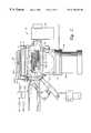
- FIG. 1is a schematic side view in partial cross section of a deposition chamber according to concepts of the present invention.
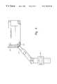
- FIG. 2is a schematic side view in cross section of the chamber of FIG. 1 showing more detail and a remote plasma cleaning cell attached.
- FIGS. 3 A- 3 Cis an electrical schematic showing three various RF matching configurations that may be used in the system of the invention.
- FIG. 4is a schematic side view in partial cross section showing the dual zone RF plasma source of the system.
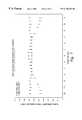
- FIG. 5is a graphical representation showing the ion current distribution produced by the coils of FIG. 4 as measured by a Langmuir probe.
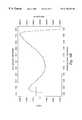
- FIG. 6 ( a ) and 6 ( b )is a graphical representation showing the deposition uniformity across the wafer plotted as a function of the use of the individual coils of FIG. 4 .
- FIG. 7is a schematic side view partially in section showing the gas control system of the invention.
- FIG. 8 ( a ) and 8 ( b )are schematic diagrams showing the HDP-CVD deposition and sputter uniformity for optimized chamber conditions plotted as standard deviation contour plots.
- FIG. 9is a schematic side view partially in section showing the microwave remote plasma clean inlet port and its location on the chamber body of the deposition chamber of FIGS. 1 and 2.
- FIGS. 10 ( a ) and ( b )are graphical representations showing (a) the wet etch uniformity of a wafer as a standard deviation contour and (b) the temperature as a function of position on the wafer during the deposition process using the system of the invention.
- FIG. 11is a graphical representation showing the temperature dependence of the oxide etch rate using both a low pressure inductive plasma cleaning technique and the remote microwave plasma cleaning technique of the invention.
- FIG. 12is a graphical representation showing the NF 3 flow rate dependence of the oxide etch rate in the deposition chamber of the present invention.
- FIG. 13is a graphical representation showing the chamber pressure dependence at constant temperature using the remote microwave plasma cleaning system of the invention.
- the HDP-CVD deposition system of the present inventionphysically comprises three major assemblies: 1) a plasma source including the gas distribution system; 2) a chamber body, including the electrostatic chuck and the pumping system; and 3) a remote microwave plasma cleaning system. These major assemblies will be discussed separately for the sake of organization, although it will be understood that in reality there is dynamic interaction between these assemblies.
- FIGS. 1 - 6various aspects of the plasma source portion of the process system of the present invention are shown.
- FIGS. 1 and 2a side view of the system 10 is shown schematically.
- the system 10includes a chamber 13 having an outer wall 12 , a cover 16 and a cantilevered, removable substrate support member 17 . These members in combination form a physically symmetric gas exhaust passage and an electrically symmetric and an evacuable enclosure for processing a substrate 18 .
- the outer wall 12is typically made of aluminum and defines an inner processing chamber 13 that has a plasma processing region 14 adjacent the upper surface of substrate 18 and its support member 17 .
- Substrate support member 17is removable through a side port 19 and has a substrate receiving portion 20 which contains an electrostatic chuck 20 a which will be discussed in more detail below.
- the base portion 52 of the substrate support member 17is mounted on the outside wall 24 of the chamber and includes an inner surface which forms a continuous inner wall with the chamber wall.
- Two separately powered RF coils, a top coil 31 and a side coil 32are wound external to a dielectric dome 33 .
- the dome 33is preferably constructed of a ceramic, such as aluminum oxide (Al 2 O 3 ) or aluminum nitride (AlN).
- the side coil 32is covered by a symmetrical ground shield 235 to reduce electrical crosstalk between the coils 31 and 32 .
- the RF coils 31 and 32are powered by two variable frequency (1.8-2.1 MHZ) RF sources 40 a and 40 b.
- the two RF power sources 40 a and 40 bare coupled to coils 31 and 32 , respectively.
- Each power sourceincludes a control circuit which measures reflected power and which adjusts a digitally controlled synthesizer in the RF generator to sweep frequencies, typically starting at 1.8 MHZ, so as to minimize the reflected power.
- the circuit conditionschange because the plasma acts as a resistor in parallel with the coil.
- the RF generatorcontinues to sweep the frequency until the minimum reflected power point is again reached.
- the power source circuitryis designed so that each set of windings resonates at or near the frequency at which the minimum reflected power point is reached, so that the voltage of the windings is high enough to drive sufficient current to sustain the plasma.
- frequency tuningguarantees that the system remains close to resonance even if the resonance point of the circuit changes during the process. In this way, frequency tuning eliminates the need for circuit tuning and impedance matching by varying the values of impedance matching components (e.g., capacitors or inductors).
- each power sourceensures that the desired power is delivered to the load despite any impedances mismatches, even continuously varying impedance mismatches which can arise due to changes in the plasma impedance.
- each RF generatordissipates the reflected power itself and increases the output power so that the delivered power remains at the desired level.
- FIGS. 3 ( a ),( b ) and ( c )three separate local RF match configurations are shown schematically.
- FIG. 3 ( a )shows a matching configuration for use with a coil L having one end grounded.
- the two capacitors C 1 and C 2form an RF voltage divider.
- a balanced coil Lhaving two shunt capacitors C 2 and C 3 , where C 2 ⁇ C 3 , across it to ground is used to match the load (plasma)frequency.
- a pi ( ⁇ ) network matchis used having two variable capacitors to ground across the coil L.
- matching networks 3 ( a ), ( b ) or ( c )can be used to transfer maximum power to plasmas ranging in impedance from as low as 5 ohms to as high as 900 ohms (in the balanced load case).
- This dual coil systemallows control of the radial ion density profiles in the reaction chamber 13 .
- FIG. 4a schematic side view of the chamber 13 is provided showing principally the coil geometry and RF feeds for top coil 31 and side coil 32 .
- the pi network matching system described in FIG. 3 ( c )is shown in FIG. 4 .
- a Langmuir probewas introduced into the chamber 13 to measure the plasma ion current at different positions across the chamber 13 using the top coil only, and the side coil only, to excite the plasma in region 13 .
- This figureclearly shows how the dual coil arrangement, when properly tuned to a substrate being processed, can generate uniform ion current across its surface. Uniform ion current across the substrate surface leads to the uniform deposition onto the wafer surface as shown in FIGS. 6 ( a ) and 6 ( b ).
- the dielectric dome 33is surmounted by a heater plate 235 A and a cold plate 235 B as shown.
- heater plate 35 a and cold plate 35 bmay be used to control the dome temperature. Control of the dome temperature to within ⁇ 10° K improves deposition adhesion and has been found to reduce flake or particle counts in the chamber.
- the dome temperatureis generally kept within the range of from about 100° C. to about 200° C. depending on processing requirements. It has been shown that higher chamber clean rates (etch rates) and better film adhesion to the substrate can also be obtained at higher dome temperatures.
- deposition gasesare introduced into the chamber through both circumferentially mounted gas nozzles 38 located near the bottom of the chamber 13 , and a centrally located gas nozzle 64 near the top of the chamber.
- gas nozzles 38located near the bottom of the chamber 13
- a centrally located gas nozzle 64near the top of the chamber.
- oxygencan be introduced along side nozzle 64 and mixed with the other gases introduced via nozzle 64 at the portion of chamber 13 .
- a first gas source 35 and a first gas controller 37control entry of the first gas into the chamber via line 39 through plenum 36 and circumferential nozzles 38 connected thereto.
- a second gas source 35 and second gas controller 37 asupply a second desired gas via line 39 a through plenum 36 a and circumferential gas nozzles 38 .
- a third gas source 58 and third gas controller 60supply a third gas via line 62 to a plenum 72 which also receives O 2 (if desired) from an O 2 source 71 and O 2 flow rate controller 73 .
- the plenum 72receives O 2 via orifice 70 and mixes it with the third gas in nozzle 64 which penetrates the chamber 13 via orifice 76 therein.
- O-ring 78sealingly attaches the plenum 72 to the outside wall of the chamber 13 .
- the third gas and O 2are mixed in the upper portion of region 13 as both gases enter the chamber.
- Both reactant and oxidizing gasesare introduced into the chamber via circumferential nozzles 38 from separate plenums 34 and 34 a as shown in FIG. 7 .
- the gas ring 38 a into which circumferential nozzles 38 are attachedis removable. This facilitates easy change of the angle which the nozzles 38 present to the plane of the wafer being processed.
- One plenumexists in the ring 38 a itself and feeds the reactant gas on both sides from a line in the chamber body for uniform initial layer properties.
- a second plenumis designed into the chamber body and feeds oxidizing gas nozzles 38 in the gas ring 38 a through single individual feed holes to each of the oxidizer nozzles.
- the ability to change the nozzle angle as well as nozzle length by changing rings 38 aallows the uniformity profile as well as the gas utilization efficiency to be varied.
- the top nozzle 64enters chamber 13 through orifice 76 as described previously. Reactant gases are fed through nozzle 64 while oxidizers, such as O 2 , can be fed as discussed previously. Independent control of top and side flows of reactant gases and oxidizing gases allows fine adjustment of the deposition film parameters and/or doping parameter uniformities of the film.
- the chamber body 24 which supports the previously described dielectric dome 33comprises two main elements.
- the first of these elementsis a body member 24 itself which provides structural support for the previously described plasma source and for the electrostatic chuck 20 a, which will be described in more detail subsequently.
- Body member 24attaches to a pumping stack comprising a twin blade throttle body 124 , a gate valve 125 and a turbomolecular pump 126 .
- the electrostatic chuck 20 ais supported by cantilever from the side of body member 24 opposite a slit valve.
- the support structure 24is designed to offer minimum obstruction to gas flow, thereby preserving as closely as possible the concept of symmetric pumping as described in co-pending, co-assigned, U.S. patent application Ser. No. 08/574,839, filed Dec. 12, 1995, which is incorporated herein by reference.
- Two side ports 127 and 128are introduced on opposite sides of the chamber wall 12 at about the level of electrostatic chuck 20 a through which the disassociated fluorine containing gases used for cleaning may be introduced. This location of the openings 127 and 128 was chosen to maximize the etch rates of deposited material on the areas of the reactor which have the thickest deposition.
- the dissociated cleaning gasesare piped internally through the chamber body from the flange inlet 127 below the slit valve 128 which allows for proper integration with any of a variety of remote plasma cells which can be attached to port 127 .
- the chamber body 24tapers down to the diameter of the flange 129 of the turbomolecular vacuum pump 126 .
- the twin blade throttle assembly 124 and gate valve 125are mounted between the chamber body member 24 and the turbomolecular pump 126 . This arrangement allows isolation (via gate valve 125 ) and/or pressure control at pressures of from about 0 to about 100 milliTorr (as determined by settings of twin blade throttle 124 ).
- the electrostatic chuck assembly 20 amaybe of the type described in co-assigned U.S. Pat. No. 5,350,479 or U.S. patent application Ser. No. 08/641,147, filed on Apr. 25, 1996, both of which are incorporated herein by reference.
- the chuck 20 aincludes helium substrate cooling, pneumatically operated, via pneumatic assembly 130 , mechanically lifted support pins 131 and RF and DC chucking bias and RF matching network 42 as required to support wafer 18 for processing.
- Wafer lift pins 131are pneumatically operated to raise or lower wafer 18 as desired by pneumatic lift controller unit 130 .
- the chuck pedestalmay comprise, for example, a dielectric coated metal body of unipolar design containing dual helium cooling zones isolated from each other. Independent temperature control of the dual zone helium substrate cooling allows promotion of very uniform temperature across a wafer 18 being processed.
- FIGS. 10 ( a ) and ( b )the wafer etch uniformity is displayed graphically as a function of standard deviation contours in FIG. 10 ( a ).
- FIG. 10 ( b )shows the corresponding temperature distribution across the wafer 18 as a function of wafer radial position.
- the body member of the electrostatic chuck 20 ais preferably maintained at about 75° C. using a piped heat exchange liquid (not shown), though the temperature may be varied as desired.
- Chuck assembly 20 acontains an RF feedthrough 133 which permits the wafer or substrate 18 to be RF biased via RF bias match unit 42 .
- RF bias match unit 42operates at the industrial frequency of 13.56 MHZ so that it is compatible with commercially available RF power supplies. However, bias match unit 42 could be mounted remotely, if desired, and could use frequencies below 3 MHZ to change the ion energy distribution in chamber 13 if desired.
- the wafer deposition system of the present inventionis provided with a remote plasma chamber cleaning system 140 .
- a remote chamber cleaning system used to advantage in the present inventionis described in U.S. patent application Ser. No. 08/278,605, filed on Jul. 21, 1994, which is incorporated herein by reference.
- a resonant microwave cavity operating typically at the industrially assigned frequency of 2.45 GHzhas a glass gas feed tube passed through it.
- the microwave energyis coupled to the selected cleaning gas flowed though the glass tube in the resonant cavity and causes excitation of the neutral atoms therein to an excited state.
- the excited gasis routed into cleaning gas feed port 127 via a connecting tube 141 of suitable material to transfer the excited gas and which is kept to the minimal length necessary to achieve this delivery.
- the etch cleaning reactions which proceed most rapidlyare of the type
- FIGS. 11, 12 and 13depict graphically the etch rate (reaction rate) as a function of gas flow (FIG. 12 ), temperature (FIG. 11) and chamber pressure (FIG. 13 ).
Landscapes
- Chemical & Material Sciences (AREA)
- Engineering & Computer Science (AREA)
- Physics & Mathematics (AREA)
- Plasma & Fusion (AREA)
- Analytical Chemistry (AREA)
- Organic Chemistry (AREA)
- Chemical Kinetics & Catalysis (AREA)
- Materials Engineering (AREA)
- Mechanical Engineering (AREA)
- Metallurgy (AREA)
- General Chemical & Material Sciences (AREA)
- Health & Medical Sciences (AREA)
- Epidemiology (AREA)
- Public Health (AREA)
- Condensed Matter Physics & Semiconductors (AREA)
- General Physics & Mathematics (AREA)
- Manufacturing & Machinery (AREA)
- Computer Hardware Design (AREA)
- Microelectronics & Electronic Packaging (AREA)
- Power Engineering (AREA)
- Drying Of Semiconductors (AREA)
- Chemical Vapour Deposition (AREA)
- Physical Vapour Deposition (AREA)
Abstract
Description
The present invention relates to an apparatus and method for processing semiconductor substrates, and more particularly, to a high density plasma (HDP) chemical vapor deposition (CVD) tool for deposition of films, preferably undoped and doped silicon dioxide, onto substrates.
Chemical vapor deposition (CVD) is a gas reaction process used in the semiconductor industry to form thin layers or films of desired materials on a substrate. High density plasma (HDP) enhanced CVD processes use a reactive chemical gas along with physical ion generation through the use of an RF generated plasma to enhance the film deposition by attraction of the positively charged plasma ions onto a negatively biased substrate surface at angles near the vertical to the surface, or at preferred angles to the surface by directional biasing of the substrate surface. In integrated circuit (IC) fabrication, the goal is to form very thin, yet uniform films onto substrates, at a high throughput. Many factors, such as the type and geometry of the power source and geometry, the gas distribution system and related exhaust, substrate heating and cooling, chamber construction, design, and symmetry, composition and temperature control of chamber surfaces, and material build up in the chamber, must be taken into consideration when evaluating a process system as well as a process which is performed by the system.
The most widely used CVD films are tungsten, silicon dioxide, silicon nitride and polysilicon, although other CVD films suitable as insulators, dielectrics, conductors, semiconductors, superconductors and magnetics are known. The system of the present invention has been found to be particularly effective in forming thin films of doped and undoped silicon dioxide.
One problem encountered in IC fabrication is the difficulty associated with establishing a uniform plasma density over the entire substrate surface during processing. As substrate sizes increase, i.e., to 300 mm, single coil assemblies suffer wall losses and the like, thereby creating inefficient coupling of power into the plasma resulting in center peaked or cusped plasma profiles. The resulting deposition of material under non-uniform plasma densities results in films which are typically center thick or edge thick, and in either instance tend to be non-uniform.
Another problem encountered in IC fabrication is uniform gas distribution over the substrate surface. Typically, a gas plenum is provided around the perimeter of a processing region and a plurality of nozzles extend radially inwardly to provide gases over the edge of the substrate surface. The gases tend to be unevenly distributed across the substrate surface, with more gas provided towards the edge of the substrate and less gas provided towards the center of the substrate. In addition, reactant gases are typically mixed in the gas injection system prior to their introduction into the chamber. In these instances, material may deposit within the gas injection system itself thereby clogging some gas injectors further heightening the gas distribution problems.
The use of a symmetric vacuum deposition system for HDP-CVD is taught in co-assigned U.S. patent application Ser. No. 08/574,839, entitled “Symmetric Chamber,” filed Dec. 12, 1995, which is incorporated herein by reference. A principal advantage of this type of system is the enhancement of uniform deposition due to symmetrical gas flow across the surface of the wafer or substrate. Ease of removal of a substrate support member and placement of a clean support member in its place without undue down time for the system is also desirable in maintaining the highest quality and turnaround time for a deposition system. The deposition system of the present invention provides this advantage also. As cleaning of the substrate support member can be particularly time consuming if done in place, a removable substrate support is very advantageous in keeping the substrate processing equipment running as continuously as possible.
Still another difficulty encountered in IC fabrication is maintaining a uniform temperature across the substrate surface. As a substrate is processed, the temperature of the substrate is typically elevated. If a temperature gradient exists across the substrate surface, the deposition of the film can proceed in a non-uniform manner. Therefore, it is important to precisely control the temperature of the substrate.
Another problem encountered in IC fabrication is the formation of extraneous particle sources in the deposition chamber itself. During processing, deposition material deposits throughout the chamber on the chamber walls, the substrate support member and on the gas distribution system components. Over time, such material build up can flake off into the chamber resulting in particle contamination on the substrate which can compromise the integrity of the devices being fabricated. Thus, the chamber must be periodically cleaned. A favored method of cleaning is to introduce cleaning gases into the chamber to react with the deposited material to form a product which can be exhausted from the chamber. Typically, a cleaning gas, such as a fluorinated gas, is introduced into the chamber and a plasma is struck in the chamber. The resultant excited products react with the deposition material to form a stable product which is then exhausted from the chamber. One problem with this process is that the cleaning is typically localized in regions adjacent to the plasma In order to enhance cleaning of all exposed chamber surfaces, the time period in which the cleaning process is performed is increased, thereby decreasing throughput, or the cleaning process is performed using high temperatures and/or pressures, thereby effectively over cleaning the chamber surfaces and increasing the cost of consumables.
Therefore, there remains a need for a process system which provides more uniform conditions for forming thin CVD films on a substrate. It would be desirable if the system incorporates a symmetric chamber having a removable substrate support, a frequency matched, tunable coil assembly to provide a uniform plasma over the substrate surface, a gas injection system to independently and uniformly introduce gases over the substrate surface, and a remote plasma source to provide a highly efficient chamber cleaning process within the chamber.
The present invention provides an HDP-CVD tool using simultaneous deposition and sputtering of doped and undoped silicon dioxide capable of excellent gap fill and blanket film deposition on wafers having sub 0.5 micron feature sizes having aspect ratios higher than 1.2:1. The system of the present invention includes: a dual RF zone inductively coupled plasma source configuration capable of producing radially tunable ion currents across the wafer; a dual zone gas distribution system to provide uniform deposition properties across the wafer surface; temperature controlled surfaces to improve film adhesion and to control extraneous particle generation; a symmetrically shaped turbomolecular pumped chamber body to eliminate gas flow or plasma ground azimuthal asymmetries; a dual helium cooling zone electrostatic chuck to provide and maintain uniform substrate temperatures during processing; an all ceramic/aluminum alloy chamber construction to eliminate chamber consumables; and a remote fluorine based plasma chamber cleaning system for high chamber cleaning rate without chuck cover plates.
So that the manner in which the above recited features, advantages and objects of the present invention are attained can be understood in detail, a more particular description of the invention, briefly summarized above, may be had by reference to the embodiments thereof which are illustrated in the appended drawings.
It is to be noted, however, that the appended drawings illustrate only typical embodiments of this invention and are, therefore, not to be considered limiting of its scope, for the invention may admit to other equally effective embodiments.
FIG. 1 is a schematic side view in partial cross section of a deposition chamber according to concepts of the present invention.
FIG. 2 is a schematic side view in cross section of the chamber of FIG. 1 showing more detail and a remote plasma cleaning cell attached.
FIGS.3A-3C is an electrical schematic showing three various RF matching configurations that may be used in the system of the invention.
FIG. 4 is a schematic side view in partial cross section showing the dual zone RF plasma source of the system.
FIG. 5 is a graphical representation showing the ion current distribution produced by the coils of FIG. 4 as measured by a Langmuir probe.
FIG.6(a) and6(b) is a graphical representation showing the deposition uniformity across the wafer plotted as a function of the use of the individual coils of FIG.4.
FIG. 7 is a schematic side view partially in section showing the gas control system of the invention.
FIG.8(a) and8(b) are schematic diagrams showing the HDP-CVD deposition and sputter uniformity for optimized chamber conditions plotted as standard deviation contour plots.
FIG. 9 is a schematic side view partially in section showing the microwave remote plasma clean inlet port and its location on the chamber body of the deposition chamber of FIGS. 1 and 2.
FIGS.10(a) and (b) are graphical representations showing (a) the wet etch uniformity of a wafer as a standard deviation contour and (b) the temperature as a function of position on the wafer during the deposition process using the system of the invention.
FIG. 11 is a graphical representation showing the temperature dependence of the oxide etch rate using both a low pressure inductive plasma cleaning technique and the remote microwave plasma cleaning technique of the invention.
FIG. 12 is a graphical representation showing the NF3flow rate dependence of the oxide etch rate in the deposition chamber of the present invention.
FIG. 13 is a graphical representation showing the chamber pressure dependence at constant temperature using the remote microwave plasma cleaning system of the invention.
The HDP-CVD deposition system of the present invention physically comprises three major assemblies: 1) a plasma source including the gas distribution system; 2) a chamber body, including the electrostatic chuck and the pumping system; and 3) a remote microwave plasma cleaning system. These major assemblies will be discussed separately for the sake of organization, although it will be understood that in reality there is dynamic interaction between these assemblies.
Plasma Source
Referring initially to FIGS.1-6, various aspects of the plasma source portion of the process system of the present invention are shown. In FIGS. 1 and 2, a side view of thesystem 10 is shown schematically. Thesystem 10 includes achamber 13 having anouter wall 12, a cover16 and a cantilevered, removablesubstrate support member 17. These members in combination form a physically symmetric gas exhaust passage and an electrically symmetric and an evacuable enclosure for processing asubstrate 18. Theouter wall 12 is typically made of aluminum and defines aninner processing chamber 13 that has aplasma processing region 14 adjacent the upper surface ofsubstrate 18 and itssupport member 17.Substrate support member 17 is removable through aside port 19 and has asubstrate receiving portion 20 which contains an electrostatic chuck20awhich will be discussed in more detail below. Thebase portion 52 of thesubstrate support member 17 is mounted on theoutside wall 24 of the chamber and includes an inner surface which forms a continuous inner wall with the chamber wall. Two separately powered RF coils, atop coil 31 and aside coil 32, are wound external to adielectric dome 33. Thedome 33 is preferably constructed of a ceramic, such as aluminum oxide (Al2O3) or aluminum nitride (AlN). Theside coil 32 is covered by a symmetrical ground shield235 to reduce electrical crosstalk between thecoils coils
Each power source includes a control circuit which measures reflected power and which adjusts a digitally controlled synthesizer in the RF generator to sweep frequencies, typically starting at 1.8 MHZ, so as to minimize the reflected power. When the plasma ignites, the circuit conditions change because the plasma acts as a resistor in parallel with the coil. At this stage, the RF generator continues to sweep the frequency until the minimum reflected power point is again reached. The power source circuitry is designed so that each set of windings resonates at or near the frequency at which the minimum reflected power point is reached, so that the voltage of the windings is high enough to drive sufficient current to sustain the plasma. Thus, frequency tuning guarantees that the system remains close to resonance even if the resonance point of the circuit changes during the process. In this way, frequency tuning eliminates the need for circuit tuning and impedance matching by varying the values of impedance matching components (e.g., capacitors or inductors).
Each power source ensures that the desired power is delivered to the load despite any impedances mismatches, even continuously varying impedance mismatches which can arise due to changes in the plasma impedance. To ensure that the correct power is delivered to the load, each RF generator dissipates the reflected power itself and increases the output power so that the delivered power remains at the desired level.
Referring now to FIGS.3(a),(b) and (c), three separate local RF match configurations are shown schematically. FIG.3(a) shows a matching configuration for use with a coil L having one end grounded. The two capacitors C1 and C2 form an RF voltage divider. In FIG.3(b), a balanced coil L having two shunt capacitors C2 and C3, where C2≈C3, across it to ground is used to match the load (plasma)frequency. Finally, in FIG.3(c) a pi (π) network match is used having two variable capacitors to ground across the coil L. Since the output impedance of most conventional RF generators is designed to be 50 ohms, matching networks3(a), (b) or (c) can be used to transfer maximum power to plasmas ranging in impedance from as low as 5 ohms to as high as 900 ohms (in the balanced load case). This dual coil system allows control of the radial ion density profiles in thereaction chamber 13.
Referring to FIG. 4, a schematic side view of thechamber 13 is provided showing principally the coil geometry and RF feeds fortop coil 31 andside coil 32. The pi network matching system described in FIG.3(c) is shown in FIG.4. As shown in FIG. 5, a Langmuir probe was introduced into thechamber 13 to measure the plasma ion current at different positions across thechamber 13 using the top coil only, and the side coil only, to excite the plasma inregion 13. This figure clearly shows how the dual coil arrangement, when properly tuned to a substrate being processed, can generate uniform ion current across its surface. Uniform ion current across the substrate surface leads to the uniform deposition onto the wafer surface as shown in FIGS.6(a) and6(b). These figures show the deposition percent deviation (from mean) as a function of position across the substrate being processed for the top coil only6(a) and for the side coil only6(b). This representation shows how if the action of the coils is superimposed, uniform plasma density results and deposition may be vastly improved.
Returning now to FIGS. 1 and 2, thedielectric dome 33 is surmounted by aheater plate 235A and acold plate 235B as shown. By direct conduction,heater plate 35aand cold plate35bmay be used to control the dome temperature. Control of the dome temperature to within ≈10° K improves deposition adhesion and has been found to reduce flake or particle counts in the chamber. The dome temperature is generally kept within the range of from about 100° C. to about 200° C. depending on processing requirements. It has been shown that higher chamber clean rates (etch rates) and better film adhesion to the substrate can also be obtained at higher dome temperatures.
Referring now to FIGS. 1,2 and7, it will be seen that deposition gases are introduced into the chamber through both circumferentially mountedgas nozzles 38 located near the bottom of thechamber 13, and a centrally locatedgas nozzle 64 near the top of the chamber. As can be seen in FIG. 7, as many as three different gases can be introduced into the chamber via thenozzles side nozzle 64 and mixed with the other gases introduced vianozzle 64 at the portion ofchamber 13. Afirst gas source 35 and afirst gas controller 37 control entry of the first gas into the chamber vialine 39 throughplenum 36 andcircumferential nozzles 38 connected thereto. Similarly, asecond gas source 35 andsecond gas controller 37asupply a second desired gas vialine 39athroughplenum 36aandcircumferential gas nozzles 38. Athird gas source 58 andthird gas controller 60 supply a third gas vialine 62 to aplenum 72 which also receives O2(if desired) from an O2source71 and O2flow rate controller 73. Theplenum 72 receives O2viaorifice 70 and mixes it with the third gas innozzle 64 which penetrates thechamber 13 viaorifice 76 therein. O-ring78 sealingly attaches theplenum 72 to the outside wall of thechamber 13. The third gas and O2are mixed in the upper portion ofregion 13 as both gases enter the chamber.
Both reactant and oxidizing gases are introduced into the chamber viacircumferential nozzles 38 fromseparate plenums gas ring 38ainto whichcircumferential nozzles 38 are attached is removable. This facilitates easy change of the angle which thenozzles 38 present to the plane of the wafer being processed. One plenum exists in thering 38aitself and feeds the reactant gas on both sides from a line in the chamber body for uniform initial layer properties. A second plenum is designed into the chamber body and feeds oxidizinggas nozzles 38 in thegas ring 38athrough single individual feed holes to each of the oxidizer nozzles. The ability to change the nozzle angle as well as nozzle length by changingrings 38aallows the uniformity profile as well as the gas utilization efficiency to be varied. Thetop nozzle 64 enterschamber 13 throughorifice 76 as described previously. Reactant gases are fed throughnozzle 64 while oxidizers, such as O2, can be fed as discussed previously. Independent control of top and side flows of reactant gases and oxidizing gases allows fine adjustment of the deposition film parameters and/or doping parameter uniformities of the film.
Chamber Body/Electrostatic Chuck Assembly
Referring again to FIGS. 1 and 2, thechamber body 24 which supports the previously describeddielectric dome 33 comprises two main elements. The first of these elements is abody member 24 itself which provides structural support for the previously described plasma source and for the electrostatic chuck20a,which will be described in more detail subsequently.Body member 24 attaches to a pumping stack comprising a twinblade throttle body 124, agate valve 125 and aturbomolecular pump 126. The electrostatic chuck20ais supported by cantilever from the side ofbody member 24 opposite a slit valve. Thesupport structure 24 is designed to offer minimum obstruction to gas flow, thereby preserving as closely as possible the concept of symmetric pumping as described in co-pending, co-assigned, U.S. patent application Ser. No. 08/574,839, filed Dec. 12, 1995, which is incorporated herein by reference.
Twoside ports 127 and128 (FIGS. 1,2, and9) are introduced on opposite sides of thechamber wall 12 at about the level of electrostatic chuck20athrough which the disassociated fluorine containing gases used for cleaning may be introduced. This location of theopenings flange inlet 127 below theslit valve 128 which allows for proper integration with any of a variety of remote plasma cells which can be attached toport 127.
Thechamber body 24 tapers down to the diameter of theflange 129 of theturbomolecular vacuum pump 126. The twinblade throttle assembly 124 andgate valve 125 are mounted between thechamber body member 24 and theturbomolecular pump 126. This arrangement allows isolation (via gate valve125) and/or pressure control at pressures of from about 0 to about 100 milliTorr (as determined by settings of twin blade throttle124).
The electrostatic chuck assembly20amaybe of the type described in co-assigned U.S. Pat. No. 5,350,479 or U.S. patent application Ser. No. 08/641,147, filed on Apr. 25, 1996, both of which are incorporated herein by reference. The chuck20aincludes helium substrate cooling, pneumatically operated, viapneumatic assembly 130, mechanically lifted support pins131 and RF and DC chucking bias andRF matching network 42 as required to supportwafer 18 for processing. Wafer lift pins131 are pneumatically operated to raise orlower wafer 18 as desired by pneumaticlift controller unit 130. The chuck pedestal may comprise, for example, a dielectric coated metal body of unipolar design containing dual helium cooling zones isolated from each other. Independent temperature control of the dual zone helium substrate cooling allows promotion of very uniform temperature across awafer 18 being processed.
Referring now to FIGS.10(a) and (b), the wafer etch uniformity is displayed graphically as a function of standard deviation contours in FIG.10(a). FIG.10(b) shows the corresponding temperature distribution across thewafer 18 as a function of wafer radial position. The body member of the electrostatic chuck20ais preferably maintained at about 75° C. using a piped heat exchange liquid (not shown), though the temperature may be varied as desired.
Chuck assembly20acontains anRF feedthrough 133 which permits the wafer orsubstrate 18 to be RF biased via RFbias match unit 42. RFbias match unit 42 operates at the industrial frequency of 13.56 MHZ so that it is compatible with commercially available RF power supplies. However,bias match unit 42 could be mounted remotely, if desired, and could use frequencies below 3 MHZ to change the ion energy distribution inchamber 13 if desired.
Remote Plasma Cleaning System
Referring now to FIGS.9-13, the wafer deposition system of the present invention is provided with a remote plasmachamber cleaning system 140. One remote chamber cleaning system used to advantage in the present invention is described in U.S. patent application Ser. No. 08/278,605, filed on Jul. 21, 1994, which is incorporated herein by reference. In microwave generated plasmas or excited gases, a resonant microwave cavity operating typically at the industrially assigned frequency of 2.45 GHz has a glass gas feed tube passed through it. The microwave energy is coupled to the selected cleaning gas flowed though the glass tube in the resonant cavity and causes excitation of the neutral atoms therein to an excited state. The excited gas is routed into cleaninggas feed port 127 via a connectingtube 141 of suitable material to transfer the excited gas and which is kept to the minimal length necessary to achieve this delivery.
In thechamber 13, the etch cleaning reactions which proceed most rapidly are of the type;
and
producing gaseous products which are removed fromchamber 13 by vacuum pumping the gas phase. The reactant gases which are most effective at producing high concentrations of long lived excited neutral Fluorine species F*are NF3, F2, SF6and ClF3. However, other cleaning gases which are excitable by microwaves and react with deposition material within the chamber may be used. For the remote microwave cleaning system of FIG. 9 in the present invention, it is preferred to use NF3and F2diluted to concentrations of from about 10% to about 50% in inert argon gas. FIGS. 11,12 and13 depict graphically the etch rate (reaction rate) as a function of gas flow (FIG.12), temperature (FIG. 11) and chamber pressure (FIG.13). Because the desired cleaning reactions produced by the use of the remote microwave excited gas cleaning system of FIG. 9 proceed without any ion bombardment of the chamber or substrate support structures, the need for cover wafers on the electrostatic chuck20a, or periodic replacement of critical chamber assemblies is avoided. Thus, a much more efficient use and throughput of the system is provided.
While the foregoing is directed to the preferred embodiment of the present invention, other and further embodiments of the invention may be devised without departing from the basic scope thereof, and the scope thereof is determined by the claims which follow.
Claims (26)
1. An apparatus for processing semiconductor substrates, comprising:
a) an enclosure comprising a sidewall and a lid, the sidewall having a first end and a second end, and the lid connected to the first end of the sidewall;
b) a substrate support member cantilever mounted on the sidewall of the enclosure, the support member having a substrate supporting surface located thereon;
c) a first gas distribution outlet positioned circumferentially about an interior surface of the sidewall between the lid and the substrate supporting surface;
d) a second gas distribution outlet disposed through the lid;
e) an exhaust port connected to the second end of the sidewall;
f) a first RF coil disposed on an exterior surface of the lid; and
g) a first frequency-tuning RF power source connected to the first RF coil.
2. The apparatus of claim1 wherein the frequency-tuning RF power source is adapted to change frequency of the RF power source in response to reflected power.
3. The apparatus of claim1 wherein the lid comprises a material selected from the group consisting of a ceramic dielectric material, aluminum oxide and aluminum nitride.
4. The apparatus of claim1, further comprising:
h) a second RF coil disposed on an exterior surface of the lid; and
i) a second frequency-tuning RF power source connected to the second RF coil.
5. The apparatus of claim4, further comprising:
j) a first RF matching network for matching the first RF power supply to the first RF coil and a second RF matching network for matching the second RF power supply to the second RF coil.
6. The apparatus of claim5 wherein each RF matching network comprises a matching network selected from the group consisting of: a pi impedance matching network, a balanced antenna impedance matching network, and a grounded antenna matching network.
7. The apparatus of claim4 wherein each frequency tuning RF power source includes a control circuit adapted to adjust a frequency of the RF power source to respond to changes in reflected power.
8. The apparatus of claim1 wherein the first RF coil comprises a concentrically wound helical coil disposed above the lid.
9. The apparatus of claim wherein the second RF coil comprises an axially wound helical coil disposed around the lid.
10. The apparatus of claim1 wherein the substrate supporting member comprises an electrostatic chuck having an RF bias power connected thereto.
11. The apparatus of claim10, wherein the substrate support member includes a dual zone substrate backside gas distribution system disposed on a substrate receiving surface for controlling substrate temperature.
12. The apparatus of claim10 further comprising:
h) a substrate RF power supply and a substrate RF matching network coupling RF power to the substrate supporting surface.
13. The apparatus of claim12 wherein the substrate RF matching network comprises a matching network selected from the group consisting of: a pi impedance matching network, a balanced antenna impedance matching network, and a grounded antenna matching network.
14. The apparatus of claim1, further comprising:
h) a cleaning gas feed port disposed on the enclosure connectable to a remote cleaning plasma source; and
i) one or more cleaning gas inlets defined within the enclosure sidewall connected to the cleaning gas feed port.
15. The apparatus of claim14 wherein the remote cleaning plasma source comprises a microwave plasma generator.
16. The apparatus of claim1 wherein the exhaust port tapers from the second end of the sidewall to a flange of an exhaust pumping stack.
17. The apparatus of claim16 wherein the pumping stack comprises a throttle assembly connected to the exhaust port, a valve connected to the throttle assembly and a vacuum pump connected to the valve.
18. The apparatus of claim17 wherein the exhaust port and the pumping stack are disposed substantially axially below the substrate support member.
19. The apparatus of claim1, further comprising:
h) a heater plate and a cold plate disposed on the chamber lid.
20. A method for processing a substrate, comprising:
a) positioning the substrate on a substrate support member that is cantilever mounted on a sidewall of a processing chamber;
b) introducing a first gas through a first gas distribution system positioned circumferentially about an interior surface of the sidewall between a chamber lid and the substrate support member;
c) introducing a second gas through a second gas distribution system disposed through the lid;
d) generating a plasma of the first and second gases introduced into the chamber using a first frequency-tuning RF power source connected to a first RF coil disposed on an exterior surface of the lid and a second frequency-tuning RF power source connected to a second coil disposed on an exterior surface of the lid, whereby a process selected from the group comprising deposition and etching is performed on the substrate; and
e) exhausting the gases through an exhaust port connected on an end opposite of the lid.
21. The method of claim20, further comprising:
f) controlling a temperature of the substrate disposed on the substrate support member using a dual zone substrate backside gas distribution system disposed on a substrate receiving surface.
22. The method of claim21, further comprising:
f) removing the substrate from the chamber; and
g) cleaning the chamber using a plasma supplied from a remote plasma source.
23. The method of claim22 wherein the remote plasma source supplies excited fluorine atoms from a cleaning gas selected from the group consisting of NF3, F2, SF6, and ClF3.
24. The method of claim23 wherein the excited fluorine atoms in the cleaning gas are diluted with argon gas to a concentration between about 10% and about 50%.
25. The method of claim20, further comprising:
f) varying a frequency of the RF power sources to respond to changes in reflected power.
26. The method of claim20, further comprising:
f) controlling a temperature of the chamber lid.
Priority Applications (8)
| Application Number | Priority Date | Filing Date | Title |
|---|---|---|---|
| US08/679,927US6170428B1 (en) | 1996-07-15 | 1996-07-15 | Symmetric tunable inductively coupled HDP-CVD reactor |
| US08/865,018US6182602B1 (en) | 1996-07-15 | 1997-05-29 | Inductively coupled HDP-CVD reactor |
| TW086110052ATW363212B (en) | 1996-07-15 | 1997-07-15 | Symmetric tunable inductively coupled HDP-CVD reactor |
| JP22293297AJP4688983B2 (en) | 1996-07-15 | 1997-07-15 | Inductively coupled HDP-CVD reactor |
| KR1019970034125AKR100268158B1 (en) | 1996-07-15 | 1997-07-15 | Inductively coupled hdp-cvd reactor |
| EP97305257AEP0819780B1 (en) | 1996-07-15 | 1997-07-15 | Inductively coupled HDP-CVD reactor |
| DE69727624TDE69727624T2 (en) | 1996-07-15 | 1997-07-15 | Inductively coupled HDP-CVD reactor |
| JP2007293616AJP2008091938A (en) | 1996-07-15 | 2007-11-12 | Process kit, wafer processing apparatus, and process kit heating method |
Applications Claiming Priority (1)
| Application Number | Priority Date | Filing Date | Title |
|---|---|---|---|
| US08/679,927US6170428B1 (en) | 1996-07-15 | 1996-07-15 | Symmetric tunable inductively coupled HDP-CVD reactor |
Related Child Applications (1)
| Application Number | Title | Priority Date | Filing Date |
|---|---|---|---|
| US08/865,018Continuation-In-PartUS6182602B1 (en) | 1996-07-15 | 1997-05-29 | Inductively coupled HDP-CVD reactor |
Publications (1)
| Publication Number | Publication Date |
|---|---|
| US6170428B1true US6170428B1 (en) | 2001-01-09 |
Family
ID=24728963
Family Applications (2)
| Application Number | Title | Priority Date | Filing Date |
|---|---|---|---|
| US08/679,927Expired - LifetimeUS6170428B1 (en) | 1996-07-15 | 1996-07-15 | Symmetric tunable inductively coupled HDP-CVD reactor |
| US08/865,018Expired - LifetimeUS6182602B1 (en) | 1996-07-15 | 1997-05-29 | Inductively coupled HDP-CVD reactor |
Family Applications After (1)
| Application Number | Title | Priority Date | Filing Date |
|---|---|---|---|
| US08/865,018Expired - LifetimeUS6182602B1 (en) | 1996-07-15 | 1997-05-29 | Inductively coupled HDP-CVD reactor |
Country Status (6)
| Country | Link |
|---|---|
| US (2) | US6170428B1 (en) |
| EP (1) | EP0819780B1 (en) |
| JP (2) | JP4688983B2 (en) |
| KR (1) | KR100268158B1 (en) |
| DE (1) | DE69727624T2 (en) |
| TW (1) | TW363212B (en) |
Cited By (262)
| Publication number | Priority date | Publication date | Assignee | Title |
|---|---|---|---|---|
| US20010010257A1 (en)* | 1998-12-30 | 2001-08-02 | Tuqiang Ni | Gas injection system for plasma processing |
| US20010019903A1 (en)* | 1996-12-23 | 2001-09-06 | Paul Kevin Shufflebotham | Inductively coupled plasma CVD |
| US20020000198A1 (en)* | 1997-05-29 | 2002-01-03 | Applied Materials, Inc. | The dome: shape and temperature controlled surfaces |
| US6362110B1 (en)* | 2000-03-30 | 2002-03-26 | Lam Research Corporation | Enhanced resist strip in a dielectric etcher using downstream plasma |
| US20020100751A1 (en)* | 2001-01-30 | 2002-08-01 | Carr Jeffrey W. | Apparatus and method for atmospheric pressure reactive atom plasma processing for surface modification |
| US20020104467A1 (en)* | 1999-02-04 | 2002-08-08 | Applied Materials, Inc. | Accelerated plasma clean |
| US20020179015A1 (en)* | 2000-05-18 | 2002-12-05 | Franz Laermer | Plasma etching system |
| US20030003244A1 (en)* | 1998-03-20 | 2003-01-02 | Applied Materials, Inc. | Staggered in-situ deposition and etching of a dielectric layer for HDP CVD |
| US20030010355A1 (en)* | 2001-07-13 | 2003-01-16 | Applied Materials, Inc | Enhanced remote plasma cleaning |
| US20030022526A1 (en)* | 2001-07-30 | 2003-01-30 | Vyvoda Michael A. | Process for fabricating a dielectric film using plasma oxidation |
| US20030029475A1 (en)* | 2001-06-01 | 2003-02-13 | Applied Materials, Inc., A Delaware Corporation | Multistep remote plasma clean process |
| US20030056900A1 (en)* | 1996-05-13 | 2003-03-27 | Applied Materials, Incorporated A Delaware Corporation | Deposition chamber and method for depositing low dielectric constant films |
| US6559052B2 (en)* | 2000-07-07 | 2003-05-06 | Applied Materials, Inc. | Deposition of amorphous silicon films by high density plasma HDP-CVD at low temperatures |
| US20030136332A1 (en)* | 2002-01-24 | 2003-07-24 | Applied Materials Inc., A Delaware Corporation | In situ application of etch back for improved deposition into high-aspect-ratio features |
| US20030157812A1 (en)* | 1998-04-21 | 2003-08-21 | Applied Materials, Inc. | Method and apparatus for modifying the profile of narrow, high-aspect-ratio gaps using RF power |
| US20030159656A1 (en)* | 2001-05-11 | 2003-08-28 | Applied Materials, Inc. | Hydrogen assisted undoped silicon oxide deposition process for HDP-CVD |
| US20030183244A1 (en)* | 2002-04-02 | 2003-10-02 | Applied Materials, Inc. | Method of cleaning a semiconductor processing chamber |
| US20030207580A1 (en)* | 2002-05-03 | 2003-11-06 | Applied Materials, Inc. | HDP-CVD dep/etch/dep process for improved deposition into high aspect ratio features |
| US20030224619A1 (en)* | 2002-06-04 | 2003-12-04 | Yoshi Ono | Method for low temperature oxidation of silicon |
| US6660177B2 (en) | 2001-11-07 | 2003-12-09 | Rapt Industries Inc. | Apparatus and method for reactive atom plasma processing for material deposition |
| US6676760B2 (en) | 2001-08-16 | 2004-01-13 | Appiled Materials, Inc. | Process chamber having multiple gas distributors and method |
| US20040079632A1 (en)* | 2002-10-23 | 2004-04-29 | Applied Materials, Inc. | High density plasma CVD process for gapfill into high aspect ratio features |
| US20040079728A1 (en)* | 2002-10-23 | 2004-04-29 | Applied Materials, Inc. | Reactive ion etching for semiconductor device feature topography modification |
| US20040079484A1 (en)* | 2001-01-19 | 2004-04-29 | Strang Eric J. | Method and apparatus for gas injection system with minimum particulate contamination |
| US6749717B1 (en) | 1997-02-04 | 2004-06-15 | Micron Technology, Inc. | Device for in-situ cleaning of an inductively-coupled plasma chambers |
| US6797188B1 (en)* | 1997-11-12 | 2004-09-28 | Meihua Shen | Self-cleaning process for etching silicon-containing material |
| US20040200499A1 (en)* | 2003-04-11 | 2004-10-14 | Applied Materials, Inc. | Backflush chamber clean |
| US20040219789A1 (en)* | 2003-02-14 | 2004-11-04 | Applied Materials, Inc. | Cleaning of native oxide with hydrogen-containing radicals |
| US20040231798A1 (en)* | 2002-09-13 | 2004-11-25 | Applied Materials, Inc. | Gas delivery system for semiconductor processing |
| US20040241342A1 (en)* | 2003-05-27 | 2004-12-02 | Applied Materials, Inc. | Methods and systems for high-aspect-ratio gapfill using atomic-oxygen generation |
| US6829056B1 (en) | 2003-08-21 | 2004-12-07 | Michael Barnes | Monitoring dimensions of features at different locations in the processing of substrates |
| US20040251236A1 (en)* | 2003-05-23 | 2004-12-16 | Applied Materials, Inc. | [deposition-selective etch-deposition process for dielectric film gapfill] |
| US20050008790A1 (en)* | 2003-01-23 | 2005-01-13 | Applied Materials, Inc. | Hydrogen assisted HDP-CVD deposition process for aggressive gap-fill technology |
| US20050014382A1 (en)* | 2003-07-16 | 2005-01-20 | Samsung Electronics Co., Ltd. | Etching apparatus and method |
| US20050048801A1 (en)* | 2003-09-03 | 2005-03-03 | Applied Materials, Inc. | In-situ-etch-assisted HDP deposition using SiF4 and hydrogen |
| US20050181632A1 (en)* | 2001-05-11 | 2005-08-18 | Applied Materials, Inc., A Delaware Corporation | HDP-CVD deposition process for filling high aspect ratio gaps |
| US20050199184A1 (en)* | 2004-03-09 | 2005-09-15 | Applied Materials, Inc. | Gas distributor having directed gas flow and cleaning method |
| US20050205211A1 (en)* | 2004-03-22 | 2005-09-22 | Vikram Singh | Plasma immersion ion implantion apparatus and method |
| US20050221618A1 (en)* | 2004-03-31 | 2005-10-06 | Amrhein Frederick J | System for controlling a plenum output flow geometry |
| US20050260356A1 (en)* | 2004-05-18 | 2005-11-24 | Applied Materials, Inc. | Microcontamination abatement in semiconductor processing |
| US20050282398A1 (en)* | 2004-06-16 | 2005-12-22 | Applied Materials, Inc., A Delaware Corporation | Oxygen plasma treatment for enhanced HDP-CVD gapfill |
| US20060006629A1 (en)* | 2004-04-30 | 2006-01-12 | Riedl Jay | Foldable stroller |
| US20060024451A1 (en)* | 2004-07-30 | 2006-02-02 | Applied Materials Inc. | Enhanced magnetic shielding for plasma-based semiconductor processing tool |
| US20060021633A1 (en)* | 2004-07-27 | 2006-02-02 | Applied Materials, Inc. | Closed loop clean gas control |
| US20060046508A1 (en)* | 2004-09-01 | 2006-03-02 | Applied Materials, Inc. A Delaware Corporation | Silicon oxide gapfill deposition using liquid precursors |
| US20060049036A1 (en)* | 2004-09-09 | 2006-03-09 | Taiwan Semiconductor Manufacturing Company, Ltd. | Method and apparatus for real-time control and monitor of deposition processes |
| US20060075967A1 (en)* | 2004-10-12 | 2006-04-13 | Applied Materials, Inc. | Magnetic-field concentration in inductively coupled plasma reactors |
| US20060105106A1 (en)* | 2004-11-16 | 2006-05-18 | Applied Materials, Inc. | Tensile and compressive stressed materials for semiconductors |
| US7052552B2 (en) | 2000-08-24 | 2006-05-30 | Applied Materials | Gas chemistry cycling to achieve high aspect ratio gapfill with HDP-CVD |
| US20060112876A1 (en)* | 2004-11-26 | 2006-06-01 | Choi Jin H | Semiconductor processing apparatus |
| US20060130756A1 (en)* | 2004-12-17 | 2006-06-22 | Applied Materials, Inc., A Delaware Corporation | Self-cooling gas delivery apparatus under high vacuum for high density plasma applications |
| US20060154494A1 (en)* | 2005-01-08 | 2006-07-13 | Applied Materials, Inc., A Delaware Corporation | High-throughput HDP-CVD processes for advanced gapfill applications |
| US20060162661A1 (en)* | 2005-01-22 | 2006-07-27 | Applied Materials, Inc. | Mixing energized and non-energized gases for silicon nitride deposition |
| US20060185591A1 (en)* | 2005-02-18 | 2006-08-24 | General Electric Company | High temperature chemical vapor deposition apparatus |
| US20060196603A1 (en)* | 2005-03-07 | 2006-09-07 | Applied Materials, Inc. | Gas baffle and distributor for semiconductor processing chamber |
| US20060225648A1 (en)* | 2004-07-01 | 2006-10-12 | Applied Materials, Inc. | Use of enhanced turbomolecular pump for gapfill deposition using high flows of low-mass fluent gas |
| US20060238954A1 (en)* | 2005-04-21 | 2006-10-26 | Applied Materials, Inc., A Delaware Corporation | Electrostatic chuck for track thermal plates |
| US20060264063A1 (en)* | 2005-05-23 | 2006-11-23 | Applied Materials, Inc. | Deposition of tensile and compressive stressed materials for semiconductors |
| US20060260645A1 (en)* | 2005-02-22 | 2006-11-23 | Appleyard Nicholas J | Methods and apparatus for processing wafers |
| US20060292894A1 (en)* | 2005-06-24 | 2006-12-28 | Applied Materials, Inc., | Gapfill using deposition-etch sequence |
| US20070037397A1 (en)* | 2005-08-11 | 2007-02-15 | Applied Materials, Inc. | Two-piece dome with separate RF coils for inductively coupled plasma reactors |
| US20070034153A1 (en)* | 2005-08-09 | 2007-02-15 | Applied Materials, Inc. | Thermal management of inductively coupled plasma reactors |
| US7205240B2 (en) | 2003-06-04 | 2007-04-17 | Applied Materials, Inc. | HDP-CVD multistep gapfill process |
| US20080000530A1 (en)* | 2006-06-02 | 2008-01-03 | Applied Materials, Inc. | Gas flow control by differential pressure measurements |
| US20080011332A1 (en)* | 2002-04-26 | 2008-01-17 | Accretech Usa, Inc. | Method and apparatus for cleaning a wafer substrate |
| US20080017316A1 (en)* | 2002-04-26 | 2008-01-24 | Accretech Usa, Inc. | Clean ignition system for wafer substrate processing |
| US20080029484A1 (en)* | 2006-07-25 | 2008-02-07 | Applied Materials, Inc. | In-situ process diagnostics of in-film aluminum during plasma deposition |
| US20080029485A1 (en)* | 2003-08-14 | 2008-02-07 | Rapt Industries, Inc. | Systems and Methods for Precision Plasma Processing |
| US20080035612A1 (en)* | 2003-08-14 | 2008-02-14 | Rapt Industries, Inc. | Systems and Methods Utilizing an Aperture with a Reactive Atom Plasma Torch |
| US20080102645A1 (en)* | 2006-10-31 | 2008-05-01 | Applied Materials, Inc. | Plasma for resist removal and facet control of underlying features |
| US7371992B2 (en) | 2003-03-07 | 2008-05-13 | Rapt Industries, Inc. | Method for non-contact cleaning of a surface |
| US20080121177A1 (en)* | 2006-11-28 | 2008-05-29 | Applied Materials, Inc. | Dual top gas feed through distributor for high density plasma chamber |
| US20080142483A1 (en)* | 2006-12-07 | 2008-06-19 | Applied Materials, Inc. | Multi-step dep-etch-dep high density plasma chemical vapor deposition processes for dielectric gapfills |
| US20080171444A1 (en)* | 2007-01-17 | 2008-07-17 | Lam Research Corporation | Apparatuses for adjusting electrode gap in capacitively-coupled RF plasma reactor |
| US20080182382A1 (en)* | 2006-12-07 | 2008-07-31 | Applied Materials, Inc. | Methods of thin film process |
| US20080190558A1 (en)* | 2002-04-26 | 2008-08-14 | Accretech Usa, Inc. | Wafer processing apparatus and method |
| US20080299775A1 (en)* | 2007-06-04 | 2008-12-04 | Applied Materials, Inc. | Gapfill extension of hdp-cvd integrated process modulation sio2 process |
| EP2034044A2 (en) | 2007-09-07 | 2009-03-11 | Applied Materials, Inc. | Impurity control in HDP-CVD DEP/ETCH/DEP processes |
| EP2034045A2 (en) | 2007-09-07 | 2009-03-11 | Applied Materials, Inc. | Reduction of etch-rate drift in HDP processes |
| US7510664B2 (en) | 2001-01-30 | 2009-03-31 | Rapt Industries, Inc. | Apparatus and method for atmospheric pressure reactive atom plasma processing for shaping of damage free surfaces |
| US20090093129A1 (en)* | 2006-11-28 | 2009-04-09 | Applied Materials, Inc. | Gas Baffle and Distributor for Semiconductor Processing Chamber |
| US7524750B2 (en) | 2006-04-17 | 2009-04-28 | Applied Materials, Inc. | Integrated process modulation (IPM) a novel solution for gapfill with HDP-CVD |
| US20090139540A1 (en)* | 2007-11-30 | 2009-06-04 | Applied Materials, Inc. | Repairing surface defects and cleaning residues from plasma chamber components |
| US20090163041A1 (en)* | 2007-12-21 | 2009-06-25 | Applied Materials, Inc. | Low wet etch rate silicon nitride film |
| US20090215281A1 (en)* | 2008-02-22 | 2009-08-27 | Applied Materials, Inc. | Hdp-cvd sion films for gap-fill |
| US20100041238A1 (en)* | 2001-10-15 | 2010-02-18 | Lam Research Corporation | Tunable multi-zone gas injection system |
| US20100041207A1 (en)* | 2008-08-18 | 2010-02-18 | Applied Materials, Inc. | High density plasma gapfill deposition-etch-deposition process using fluorocarbon etchant |
| US20100098882A1 (en)* | 2008-10-21 | 2010-04-22 | Applied Materials, Inc. | Plasma source for chamber cleaning and process |
| US20100095979A1 (en)* | 2008-10-22 | 2010-04-22 | Applied Materials, Inc. | Remote plasma clean process with cycled high and low pressure clean steps |
| US7740706B2 (en) | 2006-11-28 | 2010-06-22 | Applied Materials, Inc. | Gas baffle and distributor for semiconductor processing chamber |
| US7758698B2 (en) | 2006-11-28 | 2010-07-20 | Applied Materials, Inc. | Dual top gas feed through distributor for high density plasma chamber |
| US20100206846A1 (en)* | 2009-02-17 | 2010-08-19 | Tokyo Electron Limited | Substrate processing apparatus and substrate processing method |
| US20100270262A1 (en)* | 2009-04-22 | 2010-10-28 | Applied Materials, Inc. | Etching low-k dielectric or removing resist with a filtered ionized gas |
| US20110095689A1 (en)* | 2009-10-27 | 2011-04-28 | Tyco Healthcare Group Lp | Inductively-Coupled Plasma Device |
| US20110139751A1 (en)* | 2008-05-30 | 2011-06-16 | Colorado State Univeristy Research Foundation | Plasma-based chemical source device and method of use thereof |
| US20110140607A1 (en)* | 2008-05-30 | 2011-06-16 | Colorado State University Research Foundation | System, method and apparatus for generating plasma |
| US20130014895A1 (en)* | 2011-07-08 | 2013-01-17 | Tokyo Electron Limited | Substrate processing apparatus |
| US8497211B2 (en) | 2011-06-24 | 2013-07-30 | Applied Materials, Inc. | Integrated process modulation for PSG gapfill |
| US20130264308A1 (en)* | 2012-04-04 | 2013-10-10 | Taiwan Semiconductor Manufacturing Company, Ltd. | Plasma process, film deposition method and system using rotary chuck |
| US8679983B2 (en) | 2011-09-01 | 2014-03-25 | Applied Materials, Inc. | Selective suppression of dry-etch rate of materials containing both silicon and nitrogen |
| US8679982B2 (en) | 2011-08-26 | 2014-03-25 | Applied Materials, Inc. | Selective suppression of dry-etch rate of materials containing both silicon and oxygen |
| US8741778B2 (en) | 2010-12-14 | 2014-06-03 | Applied Materials, Inc. | Uniform dry etch in two stages |
| US8765574B2 (en) | 2012-11-09 | 2014-07-01 | Applied Materials, Inc. | Dry etch process |
| US8771539B2 (en) | 2011-02-22 | 2014-07-08 | Applied Materials, Inc. | Remotely-excited fluorine and water vapor etch |
| US8771536B2 (en) | 2011-08-01 | 2014-07-08 | Applied Materials, Inc. | Dry-etch for silicon-and-carbon-containing films |
| US8801952B1 (en) | 2013-03-07 | 2014-08-12 | Applied Materials, Inc. | Conformal oxide dry etch |
| US8808563B2 (en) | 2011-10-07 | 2014-08-19 | Applied Materials, Inc. | Selective etch of silicon by way of metastable hydrogen termination |
| US8895449B1 (en) | 2013-05-16 | 2014-11-25 | Applied Materials, Inc. | Delicate dry clean |
| US8921234B2 (en) | 2012-12-21 | 2014-12-30 | Applied Materials, Inc. | Selective titanium nitride etching |
| US8927390B2 (en) | 2011-09-26 | 2015-01-06 | Applied Materials, Inc. | Intrench profile |
| US8951429B1 (en) | 2013-10-29 | 2015-02-10 | Applied Materials, Inc. | Tungsten oxide processing |
| US8956980B1 (en) | 2013-09-16 | 2015-02-17 | Applied Materials, Inc. | Selective etch of silicon nitride |
| US8969212B2 (en) | 2012-11-20 | 2015-03-03 | Applied Materials, Inc. | Dry-etch selectivity |
| US8975152B2 (en) | 2011-11-08 | 2015-03-10 | Applied Materials, Inc. | Methods of reducing substrate dislocation during gapfill processing |
| US8980763B2 (en) | 2012-11-30 | 2015-03-17 | Applied Materials, Inc. | Dry-etch for selective tungsten removal |
| US8994270B2 (en) | 2008-05-30 | 2015-03-31 | Colorado State University Research Foundation | System and methods for plasma application |
| US8999856B2 (en) | 2011-03-14 | 2015-04-07 | Applied Materials, Inc. | Methods for etch of sin films |
| US9018108B2 (en) | 2013-01-25 | 2015-04-28 | Applied Materials, Inc. | Low shrinkage dielectric films |
| US9023732B2 (en) | 2013-03-15 | 2015-05-05 | Applied Materials, Inc. | Processing systems and methods for halide scavenging |
| US9023734B2 (en) | 2012-09-18 | 2015-05-05 | Applied Materials, Inc. | Radical-component oxide etch |
| US9028656B2 (en) | 2008-05-30 | 2015-05-12 | Colorado State University Research Foundation | Liquid-gas interface plasma device |
| US9034770B2 (en) | 2012-09-17 | 2015-05-19 | Applied Materials, Inc. | Differential silicon oxide etch |
| US9040422B2 (en) | 2013-03-05 | 2015-05-26 | Applied Materials, Inc. | Selective titanium nitride removal |
| US9064815B2 (en) | 2011-03-14 | 2015-06-23 | Applied Materials, Inc. | Methods for etch of metal and metal-oxide films |
| US9064816B2 (en) | 2012-11-30 | 2015-06-23 | Applied Materials, Inc. | Dry-etch for selective oxidation removal |
| US9111877B2 (en) | 2012-12-18 | 2015-08-18 | Applied Materials, Inc. | Non-local plasma oxide etch |
| US9117855B2 (en) | 2013-12-04 | 2015-08-25 | Applied Materials, Inc. | Polarity control for remote plasma |
| US9114438B2 (en) | 2013-05-21 | 2015-08-25 | Applied Materials, Inc. | Copper residue chamber clean |
| US9136273B1 (en) | 2014-03-21 | 2015-09-15 | Applied Materials, Inc. | Flash gate air gap |
| US9132436B2 (en) | 2012-09-21 | 2015-09-15 | Applied Materials, Inc. | Chemical control features in wafer process equipment |
| US9159606B1 (en) | 2014-07-31 | 2015-10-13 | Applied Materials, Inc. | Metal air gap |
| US9165786B1 (en) | 2014-08-05 | 2015-10-20 | Applied Materials, Inc. | Integrated oxide and nitride recess for better channel contact in 3D architectures |
| US9190293B2 (en) | 2013-12-18 | 2015-11-17 | Applied Materials, Inc. | Even tungsten etch for high aspect ratio trenches |
| US9236265B2 (en) | 2013-11-04 | 2016-01-12 | Applied Materials, Inc. | Silicon germanium processing |
| US9245762B2 (en) | 2013-12-02 | 2016-01-26 | Applied Materials, Inc. | Procedure for etch rate consistency |
| US20160027618A1 (en)* | 2014-07-24 | 2016-01-28 | Hitachi High-Technologies Corporation | Plasma processing apparatus and plasma processing method |
| US9263278B2 (en) | 2013-12-17 | 2016-02-16 | Applied Materials, Inc. | Dopant etch selectivity control |
| US9269590B2 (en) | 2014-04-07 | 2016-02-23 | Applied Materials, Inc. | Spacer formation |
| US9272359B2 (en) | 2008-05-30 | 2016-03-01 | Colorado State University Research Foundation | Liquid-gas interface plasma device |
| US9287095B2 (en) | 2013-12-17 | 2016-03-15 | Applied Materials, Inc. | Semiconductor system assemblies and methods of operation |
| US9287134B2 (en) | 2014-01-17 | 2016-03-15 | Applied Materials, Inc. | Titanium oxide etch |
| US9293568B2 (en) | 2014-01-27 | 2016-03-22 | Applied Materials, Inc. | Method of fin patterning |
| US9299582B2 (en) | 2013-11-12 | 2016-03-29 | Applied Materials, Inc. | Selective etch for metal-containing materials |
| US9299538B2 (en) | 2014-03-20 | 2016-03-29 | Applied Materials, Inc. | Radial waveguide systems and methods for post-match control of microwaves |
| US9299583B1 (en) | 2014-12-05 | 2016-03-29 | Applied Materials, Inc. | Aluminum oxide selective etch |
| US9299575B2 (en) | 2014-03-17 | 2016-03-29 | Applied Materials, Inc. | Gas-phase tungsten etch |
| US9299537B2 (en) | 2014-03-20 | 2016-03-29 | Applied Materials, Inc. | Radial waveguide systems and methods for post-match control of microwaves |
| US9309598B2 (en) | 2014-05-28 | 2016-04-12 | Applied Materials, Inc. | Oxide and metal removal |
| US9324576B2 (en) | 2010-05-27 | 2016-04-26 | Applied Materials, Inc. | Selective etch for silicon films |
| US9343272B1 (en) | 2015-01-08 | 2016-05-17 | Applied Materials, Inc. | Self-aligned process |
| US9349605B1 (en) | 2015-08-07 | 2016-05-24 | Applied Materials, Inc. | Oxide etch selectivity systems and methods |
| US9355856B2 (en) | 2014-09-12 | 2016-05-31 | Applied Materials, Inc. | V trench dry etch |
| US9355862B2 (en) | 2014-09-24 | 2016-05-31 | Applied Materials, Inc. | Fluorine-based hardmask removal |
| US9362130B2 (en) | 2013-03-01 | 2016-06-07 | Applied Materials, Inc. | Enhanced etching processes using remote plasma sources |
| US9368364B2 (en) | 2014-09-24 | 2016-06-14 | Applied Materials, Inc. | Silicon etch process with tunable selectivity to SiO2 and other materials |
| US9373522B1 (en) | 2015-01-22 | 2016-06-21 | Applied Mateials, Inc. | Titanium nitride removal |
| US9373517B2 (en) | 2012-08-02 | 2016-06-21 | Applied Materials, Inc. | Semiconductor processing with DC assisted RF power for improved control |
| US9378969B2 (en) | 2014-06-19 | 2016-06-28 | Applied Materials, Inc. | Low temperature gas-phase carbon removal |
| US9378978B2 (en) | 2014-07-31 | 2016-06-28 | Applied Materials, Inc. | Integrated oxide recess and floating gate fin trimming |
| US9385028B2 (en) | 2014-02-03 | 2016-07-05 | Applied Materials, Inc. | Air gap process |
| US9390937B2 (en) | 2012-09-20 | 2016-07-12 | Applied Materials, Inc. | Silicon-carbon-nitride selective etch |
| US9396989B2 (en) | 2014-01-27 | 2016-07-19 | Applied Materials, Inc. | Air gaps between copper lines |
| US9406523B2 (en) | 2014-06-19 | 2016-08-02 | Applied Materials, Inc. | Highly selective doped oxide removal method |
| US9425058B2 (en) | 2014-07-24 | 2016-08-23 | Applied Materials, Inc. | Simplified litho-etch-litho-etch process |
| US9449846B2 (en) | 2015-01-28 | 2016-09-20 | Applied Materials, Inc. | Vertical gate separation |
| US9478432B2 (en) | 2014-09-25 | 2016-10-25 | Applied Materials, Inc. | Silicon oxide selective removal |
| US9493879B2 (en) | 2013-07-12 | 2016-11-15 | Applied Materials, Inc. | Selective sputtering for pattern transfer |
| US9496167B2 (en) | 2014-07-31 | 2016-11-15 | Applied Materials, Inc. | Integrated bit-line airgap formation and gate stack post clean |
| US9502258B2 (en) | 2014-12-23 | 2016-11-22 | Applied Materials, Inc. | Anisotropic gap etch |
| US9499898B2 (en) | 2014-03-03 | 2016-11-22 | Applied Materials, Inc. | Layered thin film heater and method of fabrication |
| US9532826B2 (en) | 2013-03-06 | 2017-01-03 | Covidien Lp | System and method for sinus surgery |
| US9553102B2 (en) | 2014-08-19 | 2017-01-24 | Applied Materials, Inc. | Tungsten separation |
| US9555145B2 (en) | 2013-03-13 | 2017-01-31 | Covidien Lp | System and method for biofilm remediation |
| US9576809B2 (en) | 2013-11-04 | 2017-02-21 | Applied Materials, Inc. | Etch suppression with germanium |
| US9659753B2 (en) | 2014-08-07 | 2017-05-23 | Applied Materials, Inc. | Grooved insulator to reduce leakage current |
| US9691645B2 (en) | 2015-08-06 | 2017-06-27 | Applied Materials, Inc. | Bolted wafer chuck thermal management systems and methods for wafer processing systems |
| US9721789B1 (en) | 2016-10-04 | 2017-08-01 | Applied Materials, Inc. | Saving ion-damaged spacers |
| US9728437B2 (en) | 2015-02-03 | 2017-08-08 | Applied Materials, Inc. | High temperature chuck for plasma processing systems |
| US9741546B2 (en) | 2011-10-05 | 2017-08-22 | Applied Materials, Inc. | Symmetric plasma process chamber |
| US9741593B2 (en) | 2015-08-06 | 2017-08-22 | Applied Materials, Inc. | Thermal management systems and methods for wafer processing systems |
| US9768034B1 (en) | 2016-11-11 | 2017-09-19 | Applied Materials, Inc. | Removal methods for high aspect ratio structures |
| US9773648B2 (en) | 2013-08-30 | 2017-09-26 | Applied Materials, Inc. | Dual discharge modes operation for remote plasma |
| US9847289B2 (en) | 2014-05-30 | 2017-12-19 | Applied Materials, Inc. | Protective via cap for improved interconnect performance |
| US9865484B1 (en) | 2016-06-29 | 2018-01-09 | Applied Materials, Inc. | Selective etch using material modification and RF pulsing |
| US9881805B2 (en) | 2015-03-02 | 2018-01-30 | Applied Materials, Inc. | Silicon selective removal |
| US9885117B2 (en) | 2014-03-31 | 2018-02-06 | Applied Materials, Inc. | Conditioned semiconductor system parts |
| US9934942B1 (en) | 2016-10-04 | 2018-04-03 | Applied Materials, Inc. | Chamber with flow-through source |
| US9947549B1 (en) | 2016-10-10 | 2018-04-17 | Applied Materials, Inc. | Cobalt-containing material removal |
| US10026621B2 (en) | 2016-11-14 | 2018-07-17 | Applied Materials, Inc. | SiN spacer profile patterning |
| US10043684B1 (en) | 2017-02-06 | 2018-08-07 | Applied Materials, Inc. | Self-limiting atomic thermal etching systems and methods |
| US10043674B1 (en) | 2017-08-04 | 2018-08-07 | Applied Materials, Inc. | Germanium etching systems and methods |
| US10049891B1 (en) | 2017-05-31 | 2018-08-14 | Applied Materials, Inc. | Selective in situ cobalt residue removal |
| US10062585B2 (en) | 2016-10-04 | 2018-08-28 | Applied Materials, Inc. | Oxygen compatible plasma source |
| US10062579B2 (en) | 2016-10-07 | 2018-08-28 | Applied Materials, Inc. | Selective SiN lateral recess |
| US10062587B2 (en) | 2012-07-18 | 2018-08-28 | Applied Materials, Inc. | Pedestal with multi-zone temperature control and multiple purge capabilities |
| US10062575B2 (en) | 2016-09-09 | 2018-08-28 | Applied Materials, Inc. | Poly directional etch by oxidation |
| US10128086B1 (en) | 2017-10-24 | 2018-11-13 | Applied Materials, Inc. | Silicon pretreatment for nitride removal |
| US10163696B2 (en) | 2016-11-11 | 2018-12-25 | Applied Materials, Inc. | Selective cobalt removal for bottom up gapfill |
| US10170282B2 (en) | 2013-03-08 | 2019-01-01 | Applied Materials, Inc. | Insulated semiconductor faceplate designs |
| US10170336B1 (en) | 2017-08-04 | 2019-01-01 | Applied Materials, Inc. | Methods for anisotropic control of selective silicon removal |
| US10224210B2 (en) | 2014-12-09 | 2019-03-05 | Applied Materials, Inc. | Plasma processing system with direct outlet toroidal plasma source |
| US10242908B2 (en) | 2016-11-14 | 2019-03-26 | Applied Materials, Inc. | Airgap formation with damage-free copper |
| US10256079B2 (en) | 2013-02-08 | 2019-04-09 | Applied Materials, Inc. | Semiconductor processing systems having multiple plasma configurations |
| US10256112B1 (en) | 2017-12-08 | 2019-04-09 | Applied Materials, Inc. | Selective tungsten removal |
| US10283324B1 (en) | 2017-10-24 | 2019-05-07 | Applied Materials, Inc. | Oxygen treatment for nitride etching |
| US10283321B2 (en) | 2011-01-18 | 2019-05-07 | Applied Materials, Inc. | Semiconductor processing system and methods using capacitively coupled plasma |
| US10297458B2 (en) | 2017-08-07 | 2019-05-21 | Applied Materials, Inc. | Process window widening using coated parts in plasma etch processes |
| US10319739B2 (en) | 2017-02-08 | 2019-06-11 | Applied Materials, Inc. | Accommodating imperfectly aligned memory holes |
| US10319649B2 (en) | 2017-04-11 | 2019-06-11 | Applied Materials, Inc. | Optical emission spectroscopy (OES) for remote plasma monitoring |
| US10319600B1 (en) | 2018-03-12 | 2019-06-11 | Applied Materials, Inc. | Thermal silicon etch |
| US10354889B2 (en) | 2017-07-17 | 2019-07-16 | Applied Materials, Inc. | Non-halogen etching of silicon-containing materials |
| US10403507B2 (en) | 2017-02-03 | 2019-09-03 | Applied Materials, Inc. | Shaped etch profile with oxidation |
| US10410876B2 (en)* | 2016-06-24 | 2019-09-10 | Tokyo Electron Limited | Apparatus and method for processing gas, and storage medium |
| US10431429B2 (en) | 2017-02-03 | 2019-10-01 | Applied Materials, Inc. | Systems and methods for radial and azimuthal control of plasma uniformity |
| US10468267B2 (en) | 2017-05-31 | 2019-11-05 | Applied Materials, Inc. | Water-free etching methods |
| US10490418B2 (en) | 2014-10-14 | 2019-11-26 | Applied Materials, Inc. | Systems and methods for internal surface conditioning assessment in plasma processing equipment |
| US10490406B2 (en) | 2018-04-10 | 2019-11-26 | Appled Materials, Inc. | Systems and methods for material breakthrough |
| US10497573B2 (en) | 2018-03-13 | 2019-12-03 | Applied Materials, Inc. | Selective atomic layer etching of semiconductor materials |
| US10504754B2 (en) | 2016-05-19 | 2019-12-10 | Applied Materials, Inc. | Systems and methods for improved semiconductor etching and component protection |
| US10504700B2 (en) | 2015-08-27 | 2019-12-10 | Applied Materials, Inc. | Plasma etching systems and methods with secondary plasma injection |
| US10522371B2 (en) | 2016-05-19 | 2019-12-31 | Applied Materials, Inc. | Systems and methods for improved semiconductor etching and component protection |
| US10541246B2 (en) | 2017-06-26 | 2020-01-21 | Applied Materials, Inc. | 3D flash memory cells which discourage cross-cell electrical tunneling |
| US10541184B2 (en) | 2017-07-11 | 2020-01-21 | Applied Materials, Inc. | Optical emission spectroscopic techniques for monitoring etching |
| US10546729B2 (en) | 2016-10-04 | 2020-01-28 | Applied Materials, Inc. | Dual-channel showerhead with improved profile |
| US10566206B2 (en) | 2016-12-27 | 2020-02-18 | Applied Materials, Inc. | Systems and methods for anisotropic material breakthrough |
| US10573496B2 (en) | 2014-12-09 | 2020-02-25 | Applied Materials, Inc. | Direct outlet toroidal plasma source |
| US10573527B2 (en) | 2018-04-06 | 2020-02-25 | Applied Materials, Inc. | Gas-phase selective etching systems and methods |
| US10593560B2 (en) | 2018-03-01 | 2020-03-17 | Applied Materials, Inc. | Magnetic induction plasma source for semiconductor processes and equipment |
| US10593523B2 (en) | 2014-10-14 | 2020-03-17 | Applied Materials, Inc. | Systems and methods for internal surface conditioning in plasma processing equipment |
| US10595365B2 (en) | 2010-10-19 | 2020-03-17 | Applied Materials, Inc. | Chamber lid heater ring assembly |
| US10615047B2 (en) | 2018-02-28 | 2020-04-07 | Applied Materials, Inc. | Systems and methods to form airgaps |
| US10629473B2 (en) | 2016-09-09 | 2020-04-21 | Applied Materials, Inc. | Footing removal for nitride spacer |
| US10672642B2 (en) | 2018-07-24 | 2020-06-02 | Applied Materials, Inc. | Systems and methods for pedestal configuration |
| US10679870B2 (en) | 2018-02-15 | 2020-06-09 | Applied Materials, Inc. | Semiconductor processing chamber multistage mixing apparatus |
| US10699879B2 (en) | 2018-04-17 | 2020-06-30 | Applied Materials, Inc. | Two piece electrode assembly with gap for plasma control |
| US10727080B2 (en) | 2017-07-07 | 2020-07-28 | Applied Materials, Inc. | Tantalum-containing material removal |
| US10755941B2 (en) | 2018-07-06 | 2020-08-25 | Applied Materials, Inc. | Self-limiting selective etching systems and methods |
| US10854426B2 (en) | 2018-01-08 | 2020-12-01 | Applied Materials, Inc. | Metal recess for semiconductor structures |
| US10872778B2 (en) | 2018-07-06 | 2020-12-22 | Applied Materials, Inc. | Systems and methods utilizing solid-phase etchants |
| US10886137B2 (en) | 2018-04-30 | 2021-01-05 | Applied Materials, Inc. | Selective nitride removal |
| US10892198B2 (en) | 2018-09-14 | 2021-01-12 | Applied Materials, Inc. | Systems and methods for improved performance in semiconductor processing |
| US10903054B2 (en) | 2017-12-19 | 2021-01-26 | Applied Materials, Inc. | Multi-zone gas distribution systems and methods |
| US10920320B2 (en) | 2017-06-16 | 2021-02-16 | Applied Materials, Inc. | Plasma health determination in semiconductor substrate processing reactors |
| US10920319B2 (en) | 2019-01-11 | 2021-02-16 | Applied Materials, Inc. | Ceramic showerheads with conductive electrodes |
| TWI720177B (en)* | 2016-04-21 | 2021-03-01 | 日商東京威力科創股份有限公司 | Maintenance method for plasma processing device |
| US10943834B2 (en) | 2017-03-13 | 2021-03-09 | Applied Materials, Inc. | Replacement contact process |
| US10964512B2 (en) | 2018-02-15 | 2021-03-30 | Applied Materials, Inc. | Semiconductor processing chamber multistage mixing apparatus and methods |
| US11049755B2 (en) | 2018-09-14 | 2021-06-29 | Applied Materials, Inc. | Semiconductor substrate supports with embedded RF shield |
| US11062887B2 (en) | 2018-09-17 | 2021-07-13 | Applied Materials, Inc. | High temperature RF heater pedestals |
| US11121002B2 (en) | 2018-10-24 | 2021-09-14 | Applied Materials, Inc. | Systems and methods for etching metals and metal derivatives |
| US11239061B2 (en) | 2014-11-26 | 2022-02-01 | Applied Materials, Inc. | Methods and systems to enhance process uniformity |
| US11257693B2 (en) | 2015-01-09 | 2022-02-22 | Applied Materials, Inc. | Methods and systems to improve pedestal temperature control |
| US11276590B2 (en) | 2017-05-17 | 2022-03-15 | Applied Materials, Inc. | Multi-zone semiconductor substrate supports |
| US11276559B2 (en) | 2017-05-17 | 2022-03-15 | Applied Materials, Inc. | Semiconductor processing chamber for multiple precursor flow |
| US11328909B2 (en) | 2017-12-22 | 2022-05-10 | Applied Materials, Inc. | Chamber conditioning and removal processes |
| US11417534B2 (en) | 2018-09-21 | 2022-08-16 | Applied Materials, Inc. | Selective material removal |
| US11437242B2 (en) | 2018-11-27 | 2022-09-06 | Applied Materials, Inc. | Selective removal of silicon-containing materials |
| US11594428B2 (en) | 2015-02-03 | 2023-02-28 | Applied Materials, Inc. | Low temperature chuck for plasma processing systems |
| US11682560B2 (en) | 2018-10-11 | 2023-06-20 | Applied Materials, Inc. | Systems and methods for hafnium-containing film removal |
| US11721527B2 (en) | 2019-01-07 | 2023-08-08 | Applied Materials, Inc. | Processing chamber mixing systems |
| US12227840B2 (en) | 2016-11-29 | 2025-02-18 | Lam Research Corporation | Substrate support with varying depths of areas between mesas and corresponding temperature dependent method of fabricating |
| US12340979B2 (en) | 2017-05-17 | 2025-06-24 | Applied Materials, Inc. | Semiconductor processing chamber for improved precursor flow |
Families Citing this family (68)
| Publication number | Priority date | Publication date | Assignee | Title |
|---|---|---|---|---|
| US6170428B1 (en)* | 1996-07-15 | 2001-01-09 | Applied Materials, Inc. | Symmetric tunable inductively coupled HDP-CVD reactor |
| EP0926716B1 (en)* | 1997-12-17 | 2003-07-16 | Tokyo Electron Limited | Method of processing a semiconductor substrate |
| WO1999054521A2 (en)* | 1998-04-21 | 1999-10-28 | Applied Materials, Inc. | Method and apparatus for modifying the profile of high-aspect-ratio gaps using differential plasma power |
| KR100296137B1 (en)* | 1998-06-16 | 2001-08-07 | 박종섭 | method for fabricating semiconductor device having HDP-CVD oxide layer as passivation layer |
| US6367413B1 (en) | 1999-06-15 | 2002-04-09 | Tokyo Electron Limited | Apparatus for monitoring substrate biasing during plasma processing of a substrate |
| US6395095B1 (en) | 1999-06-15 | 2002-05-28 | Tokyo Electron Limited | Process apparatus and method for improved plasma processing of a substrate |
| US6431112B1 (en) | 1999-06-15 | 2002-08-13 | Tokyo Electron Limited | Apparatus and method for plasma processing of a substrate utilizing an electrostatic chuck |
| EP1230663A1 (en)* | 1999-11-15 | 2002-08-14 | LAM Research Corporation | Temperature control system for plasma processing apparatus |
| US6302966B1 (en) | 1999-11-15 | 2001-10-16 | Lam Research Corporation | Temperature control system for plasma processing apparatus |
| TW518639B (en)* | 1999-11-18 | 2003-01-21 | Tokyo Electron Ltd | Heat treatment device, cooling treatment device and cooling treatment method |
| KR20010062209A (en)* | 1999-12-10 | 2001-07-07 | 히가시 데쓰로 | Processing apparatus with a chamber having therein a high-etching resistant sprayed film |
| US6372291B1 (en)* | 1999-12-23 | 2002-04-16 | Applied Materials, Inc. | In situ deposition and integration of silicon nitride in a high density plasma reactor |
| EP1169490B1 (en) | 2000-01-12 | 2008-03-12 | Tokyo Electron Limited | Vacuum processing apparatus |
| KR100704591B1 (en)* | 2000-03-21 | 2007-04-09 | 주성엔지니어링(주) | CD device and internal cleaning method |
| US20030010354A1 (en) | 2000-03-27 | 2003-01-16 | Applied Materials, Inc. | Fluorine process for cleaning semiconductor process chamber |
| US6843258B2 (en) | 2000-12-19 | 2005-01-18 | Applied Materials, Inc. | On-site cleaning gas generation for process chamber cleaning |
| US20020144706A1 (en)* | 2001-04-10 | 2002-10-10 | Davis Matthew F. | Remote plasma cleaning of pumpstack components of a reactor chamber |
| KR100397047B1 (en)* | 2001-05-08 | 2003-09-02 | 삼성전자주식회사 | Chiller of electrostatic chuck and chilling method thereof |
| US6577113B2 (en) | 2001-06-06 | 2003-06-10 | Tokyo Electron Limited | Apparatus and method for measuring substrate biasing during plasma processing of a substrate |
| US6936842B2 (en)* | 2001-06-27 | 2005-08-30 | Applied Materials, Inc. | Method and apparatus for process monitoring |
| DE10141142B4 (en)* | 2001-08-24 | 2004-11-11 | Roth & Rau Ag | Device for reactive plasma treatment of substrates and method for use |
| DE10216786C5 (en)* | 2002-04-15 | 2009-10-15 | Ers Electronic Gmbh | Method and apparatus for conditioning semiconductor wafers and / or hybrids |
| US20040040664A1 (en)* | 2002-06-03 | 2004-03-04 | Yang Jang Gyoo | Cathode pedestal for a plasma etch reactor |
| JP3820188B2 (en) | 2002-06-19 | 2006-09-13 | 三菱重工業株式会社 | Plasma processing apparatus and plasma processing method |
| TWI235433B (en)* | 2002-07-17 | 2005-07-01 | Tokyo Electron Ltd | Oxide film forming method, oxide film forming apparatus and electronic device material |
| KR100756095B1 (en)* | 2003-05-02 | 2007-09-05 | 동경 엘렉트론 주식회사 | Process gas introducing mechanism and plasma processing device |
| US7993460B2 (en)* | 2003-06-30 | 2011-08-09 | Lam Research Corporation | Substrate support having dynamic temperature control |
| KR20060064047A (en)* | 2003-08-08 | 2006-06-12 | 세키스이가가쿠 고교가부시키가이샤 | Plasma processing method and apparatus |
| JP2005063760A (en)* | 2003-08-08 | 2005-03-10 | Sekisui Chem Co Ltd | Plasma treatment method and treatment device |
| JP4532948B2 (en)* | 2004-03-19 | 2010-08-25 | 積水化学工業株式会社 | Plasma processing method |
| US20050079729A1 (en)* | 2003-10-08 | 2005-04-14 | Woo-Sung Jang | High density plasma oxide film deposition apparatus having a guide ring and a semiconductor device manufacturing method using the same |
| TW200526800A (en)* | 2003-12-15 | 2005-08-16 | Applied Materials Inc | Edge flow faceplate for improvement of CVD film properties |
| US8083853B2 (en) | 2004-05-12 | 2011-12-27 | Applied Materials, Inc. | Plasma uniformity control by gas diffuser hole design |
| US20060005771A1 (en)* | 2004-07-12 | 2006-01-12 | Applied Materials, Inc. | Apparatus and method of shaping profiles of large-area PECVD electrodes |
| US8074599B2 (en)* | 2004-05-12 | 2011-12-13 | Applied Materials, Inc. | Plasma uniformity control by gas diffuser curvature |
| US8328939B2 (en)* | 2004-05-12 | 2012-12-11 | Applied Materials, Inc. | Diffuser plate with slit valve compensation |
| US7429410B2 (en) | 2004-09-20 | 2008-09-30 | Applied Materials, Inc. | Diffuser gravity support |
| KR100589046B1 (en)* | 2004-09-23 | 2006-06-12 | 삼성전자주식회사 | Thin Film Formation Method |
| KR100842739B1 (en)* | 2006-05-02 | 2008-07-01 | 주식회사 하이닉스반도체 | Electrostatic chuck of high density plasma deposition apparatus |
| US7879184B2 (en)* | 2006-06-20 | 2011-02-01 | Lam Research Corporation | Apparatuses, systems and methods for rapid cleaning of plasma confinement rings with minimal erosion of other chamber parts |
| US8038850B2 (en)* | 2006-06-23 | 2011-10-18 | Qimonda Ag | Sputter deposition method for forming integrated circuit |
| KR101046520B1 (en) | 2007-09-07 | 2011-07-04 | 어플라이드 머티어리얼스, 인코포레이티드 | Source gas flow path control in pecvd system to control a by-product film deposition on inside chamber |
| CN101351076B (en)* | 2008-09-16 | 2011-08-17 | 北京北方微电子基地设备工艺研究中心有限责任公司 | Apparatus for processing plasma |
| DE102009044276A1 (en)* | 2009-10-16 | 2011-05-05 | Aixtron Ag | CVD reactor with multi-zone gas cushion substrate holder |
| US20110226617A1 (en)* | 2010-03-22 | 2011-09-22 | Applied Materials, Inc. | Dielectric deposition using a remote plasma source |
| JP5685405B2 (en)* | 2010-09-03 | 2015-03-18 | 株式会社日立ハイテクノロジーズ | Vacuum processing equipment |
| US9719169B2 (en) | 2010-12-20 | 2017-08-01 | Novellus Systems, Inc. | System and apparatus for flowable deposition in semiconductor fabrication |
| US10727092B2 (en)* | 2012-10-17 | 2020-07-28 | Applied Materials, Inc. | Heated substrate support ring |
| TWI474368B (en)* | 2012-12-27 | 2015-02-21 | Metal Ind Res & Dev Ct | Plasma treatment system and rf impedance matching apparatus |
| CN105122431A (en)* | 2013-03-13 | 2015-12-02 | 应用材料公司 | Pulsed pc plasma etching process and apparatus |
| US9847222B2 (en) | 2013-10-25 | 2017-12-19 | Lam Research Corporation | Treatment for flowable dielectric deposition on substrate surfaces |
| US10049921B2 (en) | 2014-08-20 | 2018-08-14 | Lam Research Corporation | Method for selectively sealing ultra low-k porous dielectric layer using flowable dielectric film formed from vapor phase dielectric precursor |
| US9916977B2 (en) | 2015-11-16 | 2018-03-13 | Lam Research Corporation | Low k dielectric deposition via UV driven photopolymerization |
| US10388546B2 (en) | 2015-11-16 | 2019-08-20 | Lam Research Corporation | Apparatus for UV flowable dielectric |
| JP6595396B2 (en)* | 2016-04-21 | 2019-10-23 | 東京エレクトロン株式会社 | Plasma processing equipment |
| US11017984B2 (en) | 2016-04-28 | 2021-05-25 | Applied Materials, Inc. | Ceramic coated quartz lid for processing chamber |
| CN110612593B (en)* | 2017-05-31 | 2022-09-13 | 应用材料公司 | Remote plasma oxidation chamber |
| US11955362B2 (en) | 2017-09-13 | 2024-04-09 | Applied Materials, Inc. | Substrate support for reduced damage substrate backside |
| CN108048820A (en)* | 2017-12-22 | 2018-05-18 | 江苏鲁汶仪器有限公司 | Vapor deposition apparatus and vapor deposition method |
| CN112017932B (en)* | 2019-05-31 | 2022-11-29 | 中微半导体设备(上海)股份有限公司 | Corrosion-resistant structure of gas delivery system in plasma processing device |
| US11610792B2 (en)* | 2019-08-16 | 2023-03-21 | Applied Materials, Inc. | Heated substrate support with thermal baffles |
| WO2021131097A1 (en)* | 2019-12-25 | 2021-07-01 | 三菱電機株式会社 | Microwave plasma treatment device |
| CN116917533A (en)* | 2021-02-19 | 2023-10-20 | 应用材料公司 | Substrate support, method of processing substrate, and processing system |
| KR20240001171A (en)* | 2021-04-26 | 2024-01-03 | 도쿄엘렉트론가부시키가이샤 | Substrate processing device and substrate processing method |
| US11917744B2 (en)* | 2021-07-22 | 2024-02-27 | Perkinelmer Scientific Canada Ulc | Heat management for inductively coupled plasma systems |
| DE102022102768A1 (en)* | 2022-02-07 | 2023-08-10 | Stephan Wege | Symmetrical process reactor |
| JP7358576B1 (en) | 2022-07-21 | 2023-10-10 | 積水化学工業株式会社 | Film deposition equipment and method for manufacturing film-coated wafers |
| KR102760147B1 (en)* | 2022-11-09 | 2025-02-03 | 세메스 주식회사 | Substrate supporting unit, apparatus for processing substrate including the same, and ring transfer method |
Citations (21)
| Publication number | Priority date | Publication date | Assignee | Title |
|---|---|---|---|---|
| US4808258A (en)* | 1983-10-19 | 1989-02-28 | Hitachi, Ltd. | Plasma processing method and apparatus for carrying out the same |
| US4878994A (en)* | 1987-07-16 | 1989-11-07 | Texas Instruments Incorporated | Method for etching titanium nitride local interconnects |
| US5242561A (en)* | 1989-12-15 | 1993-09-07 | Canon Kabushiki Kaisha | Plasma processing method and plasma processing apparatus |
| US5365057A (en) | 1993-07-02 | 1994-11-15 | Litton Systems, Inc. | Light-weight night vision device |
| US5401350A (en)* | 1993-03-08 | 1995-03-28 | Lsi Logic Corporation | Coil configurations for improved uniformity in inductively coupled plasma systems |
| US5403434A (en)* | 1994-01-06 | 1995-04-04 | Texas Instruments Incorporated | Low-temperature in-situ dry cleaning process for semiconductor wafer |
| JPH07161695A (en) | 1993-12-02 | 1995-06-23 | Tokyo Electron Ltd | Plasma process method |
| EP0660449A2 (en) | 1993-12-09 | 1995-06-28 | Santa Barbara Research Center | Electrical feedthrough and its manufacture, and apparatus utilizing the feedthrough |
| EP0668608A1 (en) | 1994-02-22 | 1995-08-23 | Applied Materials, Inc. | Electrostatic chuck with erosion-resistant electrode connection |
| EP0697467A1 (en) | 1994-07-21 | 1996-02-21 | Applied Materials, Inc. | Method and apparatus for cleaning a deposition chamber |
| WO1997003224A1 (en) | 1995-07-10 | 1997-01-30 | Watkins Johnson Company | A plasma enhanced chemical processing reactor and method |
| US5665167A (en)* | 1993-02-16 | 1997-09-09 | Tokyo Electron Kabushiki Kaisha | Plasma treatment apparatus having a workpiece-side electrode grounding circuit |
| US5669975A (en)* | 1996-03-27 | 1997-09-23 | Sony Corporation | Plasma producing method and apparatus including an inductively-coupled plasma source |
| US5688357A (en)* | 1995-02-15 | 1997-11-18 | Applied Materials, Inc. | Automatic frequency tuning of an RF power source of an inductively coupled plasma reactor |
| US5709757A (en)* | 1994-08-25 | 1998-01-20 | Tokyo Electron Limited | Film forming and dry cleaning apparatus and method |
| US5753044A (en)* | 1995-02-15 | 1998-05-19 | Applied Materials, Inc. | RF plasma reactor with hybrid conductor and multi-radius dome ceiling |
| US5756400A (en)* | 1995-12-08 | 1998-05-26 | Applied Materials, Inc. | Method and apparatus for cleaning by-products from plasma chamber surfaces |
| US5767628A (en)* | 1995-12-20 | 1998-06-16 | International Business Machines Corporation | Helicon plasma processing tool utilizing a ferromagnetic induction coil with an internal cooling channel |
| US5770100A (en)* | 1989-08-28 | 1998-06-23 | Fukuyama; Ryooji | Method of treating samples |
| US5792261A (en)* | 1993-12-17 | 1998-08-11 | Tokyo Electron Limited | Plasma process apparatus |
| US6027601A (en)* | 1997-07-01 | 2000-02-22 | Applied Materials, Inc | Automatic frequency tuning of an RF plasma source of an inductively coupled plasma reactor |
Family Cites Families (12)
| Publication number | Priority date | Publication date | Assignee | Title |
|---|---|---|---|---|
| JPS63119525A (en)* | 1986-11-08 | 1988-05-24 | Hitachi Electronics Eng Co Ltd | Plasma cvd apparatus |
| JP2680338B2 (en)* | 1988-03-31 | 1997-11-19 | 株式会社東芝 | Electrostatic chuck device |
| JP2635267B2 (en)* | 1991-06-27 | 1997-07-30 | アプライド マテリアルズ インコーポレイテッド | RF plasma processing equipment |
| JP2764524B2 (en)* | 1993-09-28 | 1998-06-11 | 名古屋大学長 | Radical control device |
| JP3276023B2 (en)* | 1993-10-20 | 2002-04-22 | 東京エレクトロン株式会社 | Control method of plasma processing apparatus |
| JP3043217B2 (en)* | 1994-02-22 | 2000-05-22 | 東京エレクトロン株式会社 | Plasma generator |
| US5463525A (en)* | 1993-12-20 | 1995-10-31 | International Business Machines Corporation | Guard ring electrostatic chuck |
| JP3276514B2 (en)* | 1994-04-26 | 2002-04-22 | 東京エレクトロン株式会社 | Plasma processing equipment |
| EP0680072B1 (en)* | 1994-04-28 | 2003-10-08 | Applied Materials, Inc. | A method of operating a high density plasma CVD reactor with combined inductive and capacitive coupling |
| JPH07335563A (en)* | 1994-06-10 | 1995-12-22 | Mitsubishi Electric Corp | Plasma CVD equipment |
| US5824604A (en)* | 1996-01-23 | 1998-10-20 | Mattson Technology, Inc. | Hydrocarbon-enhanced dry stripping of photoresist |
| US6170428B1 (en)* | 1996-07-15 | 2001-01-09 | Applied Materials, Inc. | Symmetric tunable inductively coupled HDP-CVD reactor |
- 1996
- 1996-07-15USUS08/679,927patent/US6170428B1/ennot_activeExpired - Lifetime
- 1997
- 1997-05-29USUS08/865,018patent/US6182602B1/ennot_activeExpired - Lifetime
- 1997-07-15TWTW086110052Apatent/TW363212B/ennot_activeIP Right Cessation
- 1997-07-15EPEP97305257Apatent/EP0819780B1/ennot_activeExpired - Lifetime
- 1997-07-15KRKR1019970034125Apatent/KR100268158B1/ennot_activeExpired - Lifetime
- 1997-07-15DEDE69727624Tpatent/DE69727624T2/ennot_activeExpired - Lifetime
- 1997-07-15JPJP22293297Apatent/JP4688983B2/ennot_activeExpired - Fee Related
- 2007
- 2007-11-12JPJP2007293616Apatent/JP2008091938A/enactivePending
Patent Citations (22)
| Publication number | Priority date | Publication date | Assignee | Title |
|---|---|---|---|---|
| US4808258A (en)* | 1983-10-19 | 1989-02-28 | Hitachi, Ltd. | Plasma processing method and apparatus for carrying out the same |
| US4878994A (en)* | 1987-07-16 | 1989-11-07 | Texas Instruments Incorporated | Method for etching titanium nitride local interconnects |
| US5770100A (en)* | 1989-08-28 | 1998-06-23 | Fukuyama; Ryooji | Method of treating samples |
| US5242561A (en)* | 1989-12-15 | 1993-09-07 | Canon Kabushiki Kaisha | Plasma processing method and plasma processing apparatus |
| US5665167A (en)* | 1993-02-16 | 1997-09-09 | Tokyo Electron Kabushiki Kaisha | Plasma treatment apparatus having a workpiece-side electrode grounding circuit |
| US5401350A (en)* | 1993-03-08 | 1995-03-28 | Lsi Logic Corporation | Coil configurations for improved uniformity in inductively coupled plasma systems |
| US5365057A (en) | 1993-07-02 | 1994-11-15 | Litton Systems, Inc. | Light-weight night vision device |
| JPH07161695A (en) | 1993-12-02 | 1995-06-23 | Tokyo Electron Ltd | Plasma process method |
| EP0660449A2 (en) | 1993-12-09 | 1995-06-28 | Santa Barbara Research Center | Electrical feedthrough and its manufacture, and apparatus utilizing the feedthrough |
| US5792261A (en)* | 1993-12-17 | 1998-08-11 | Tokyo Electron Limited | Plasma process apparatus |
| US5403434A (en)* | 1994-01-06 | 1995-04-04 | Texas Instruments Incorporated | Low-temperature in-situ dry cleaning process for semiconductor wafer |
| EP0668608A1 (en) | 1994-02-22 | 1995-08-23 | Applied Materials, Inc. | Electrostatic chuck with erosion-resistant electrode connection |
| EP0697467A1 (en) | 1994-07-21 | 1996-02-21 | Applied Materials, Inc. | Method and apparatus for cleaning a deposition chamber |
| US5709757A (en)* | 1994-08-25 | 1998-01-20 | Tokyo Electron Limited | Film forming and dry cleaning apparatus and method |
| US5753044A (en)* | 1995-02-15 | 1998-05-19 | Applied Materials, Inc. | RF plasma reactor with hybrid conductor and multi-radius dome ceiling |
| US5688357A (en)* | 1995-02-15 | 1997-11-18 | Applied Materials, Inc. | Automatic frequency tuning of an RF power source of an inductively coupled plasma reactor |
| US5792272A (en)* | 1995-07-10 | 1998-08-11 | Watkins-Johnson Company | Plasma enhanced chemical processing reactor and method |
| WO1997003224A1 (en) | 1995-07-10 | 1997-01-30 | Watkins Johnson Company | A plasma enhanced chemical processing reactor and method |
| US5756400A (en)* | 1995-12-08 | 1998-05-26 | Applied Materials, Inc. | Method and apparatus for cleaning by-products from plasma chamber surfaces |
| US5767628A (en)* | 1995-12-20 | 1998-06-16 | International Business Machines Corporation | Helicon plasma processing tool utilizing a ferromagnetic induction coil with an internal cooling channel |
| US5669975A (en)* | 1996-03-27 | 1997-09-23 | Sony Corporation | Plasma producing method and apparatus including an inductively-coupled plasma source |
| US6027601A (en)* | 1997-07-01 | 2000-02-22 | Applied Materials, Inc | Automatic frequency tuning of an RF plasma source of an inductively coupled plasma reactor |
Non-Patent Citations (3)
| Title |
|---|
| EP Search Report dated Apr. 14, 1998. |
| EP Search Report dated Nov. 11, 1997. |
| Lucovsky, G., et al., "Deposition of silicon dioxide and silicon nitride by remote plasma enhanced chemical vapor deposition," Journal of Vacuum Science & Technology, vol. 4, No. 3, May-Jun. (1986). |
Cited By (429)
| Publication number | Priority date | Publication date | Assignee | Title |
|---|---|---|---|---|
| US20030056900A1 (en)* | 1996-05-13 | 2003-03-27 | Applied Materials, Incorporated A Delaware Corporation | Deposition chamber and method for depositing low dielectric constant films |
| US6833052B2 (en)* | 1996-05-13 | 2004-12-21 | Applied Materials, Inc. | Deposition chamber and method for depositing low dielectric constant films |
| US20050150454A1 (en)* | 1996-05-13 | 2005-07-14 | Applied Materials, Inc. | Deposition chamber and method for depositing low dielectric constant films |
| US7413627B2 (en) | 1996-05-13 | 2008-08-19 | Applied Materials, Inc. | Deposition chamber and method for depositing low dielectric constant films |
| US20010019903A1 (en)* | 1996-12-23 | 2001-09-06 | Paul Kevin Shufflebotham | Inductively coupled plasma CVD |
| US6749717B1 (en) | 1997-02-04 | 2004-06-15 | Micron Technology, Inc. | Device for in-situ cleaning of an inductively-coupled plasma chambers |
| US20020000198A1 (en)* | 1997-05-29 | 2002-01-03 | Applied Materials, Inc. | The dome: shape and temperature controlled surfaces |
| US6797188B1 (en)* | 1997-11-12 | 2004-09-28 | Meihua Shen | Self-cleaning process for etching silicon-containing material |
| US20070071908A1 (en)* | 1998-03-20 | 2007-03-29 | Applied Materials, Inc. | Staggered in-situ deposition and etching of a dielectric layer for HDP-CVD |
| US6821577B2 (en) | 1998-03-20 | 2004-11-23 | Applied Materials, Inc. | Staggered in-situ deposition and etching of a dielectric layer for HDP CVD |
| US20030003244A1 (en)* | 1998-03-20 | 2003-01-02 | Applied Materials, Inc. | Staggered in-situ deposition and etching of a dielectric layer for HDP CVD |
| US7132134B2 (en) | 1998-03-20 | 2006-11-07 | Applied Materials, Inc. | Staggered in-situ deposition and etching of a dielectric layer for HDP CVD |
| US7455893B2 (en) | 1998-03-20 | 2008-11-25 | Applied Materials, Inc. | Staggered in-situ deposition and etching of a dielectric layer for HDP-CVD |
| US20050032382A1 (en)* | 1998-03-20 | 2005-02-10 | Applied Materials, Inc. | Staggered in-situ deposition and etching of a dielectric layer for HDP CVD |
| US20030157812A1 (en)* | 1998-04-21 | 2003-08-21 | Applied Materials, Inc. | Method and apparatus for modifying the profile of narrow, high-aspect-ratio gaps using RF power |
| US8025731B2 (en) | 1998-12-30 | 2011-09-27 | Lam Research Corporation | Gas injection system for plasma processing |
| US20010010257A1 (en)* | 1998-12-30 | 2001-08-02 | Tuqiang Ni | Gas injection system for plasma processing |
| US20100327085A1 (en)* | 1998-12-30 | 2010-12-30 | Lam Research Corporation, | Gas injection system for plasma processing |
| US7785417B2 (en) | 1998-12-30 | 2010-08-31 | Lam Research Corporation | Gas injection system for plasma processing |
| US6814087B2 (en) | 1999-02-04 | 2004-11-09 | Applied Materials, Inc. | Accelerated plasma clean |
| US20050103266A1 (en)* | 1999-02-04 | 2005-05-19 | Applied Materials, Inc. | Accelerated plasma clean |
| US7506654B2 (en) | 1999-02-04 | 2009-03-24 | Applied Materials, Inc. | Accelerated plasma clean |
| US20020104467A1 (en)* | 1999-02-04 | 2002-08-08 | Applied Materials, Inc. | Accelerated plasma clean |
| US6362110B1 (en)* | 2000-03-30 | 2002-03-26 | Lam Research Corporation | Enhanced resist strip in a dielectric etcher using downstream plasma |
| US20020179015A1 (en)* | 2000-05-18 | 2002-12-05 | Franz Laermer | Plasma etching system |
| US6559052B2 (en)* | 2000-07-07 | 2003-05-06 | Applied Materials, Inc. | Deposition of amorphous silicon films by high density plasma HDP-CVD at low temperatures |
| US7052552B2 (en) | 2000-08-24 | 2006-05-30 | Applied Materials | Gas chemistry cycling to achieve high aspect ratio gapfill with HDP-CVD |
| US7563328B2 (en)* | 2001-01-19 | 2009-07-21 | Tokyo Electron Limited | Method and apparatus for gas injection system with minimum particulate contamination |
| US20040079484A1 (en)* | 2001-01-19 | 2004-04-29 | Strang Eric J. | Method and apparatus for gas injection system with minimum particulate contamination |
| US20050000656A1 (en)* | 2001-01-30 | 2005-01-06 | Rapt Industries, Inc. | Apparatus for atmospheric pressure reactive atom plasma processing for surface modification |
| US20020100751A1 (en)* | 2001-01-30 | 2002-08-01 | Carr Jeffrey W. | Apparatus and method for atmospheric pressure reactive atom plasma processing for surface modification |
| US7591957B2 (en) | 2001-01-30 | 2009-09-22 | Rapt Industries, Inc. | Method for atmospheric pressure reactive atom plasma processing for surface modification |
| US7510664B2 (en) | 2001-01-30 | 2009-03-31 | Rapt Industries, Inc. | Apparatus and method for atmospheric pressure reactive atom plasma processing for shaping of damage free surfaces |
| US7196021B2 (en) | 2001-05-11 | 2007-03-27 | Applied Materials, Inc. | HDP-CVD deposition process for filling high aspect ratio gaps |
| US20030159656A1 (en)* | 2001-05-11 | 2003-08-28 | Applied Materials, Inc. | Hydrogen assisted undoped silicon oxide deposition process for HDP-CVD |
| US20050181632A1 (en)* | 2001-05-11 | 2005-08-18 | Applied Materials, Inc., A Delaware Corporation | HDP-CVD deposition process for filling high aspect ratio gaps |
| US6929700B2 (en) | 2001-05-11 | 2005-08-16 | Applied Materials, Inc. | Hydrogen assisted undoped silicon oxide deposition process for HDP-CVD |
| US20030029475A1 (en)* | 2001-06-01 | 2003-02-13 | Applied Materials, Inc., A Delaware Corporation | Multistep remote plasma clean process |
| US7159597B2 (en) | 2001-06-01 | 2007-01-09 | Applied Materials, Inc. | Multistep remote plasma clean process |
| US20030010355A1 (en)* | 2001-07-13 | 2003-01-16 | Applied Materials, Inc | Enhanced remote plasma cleaning |
| US6868856B2 (en) | 2001-07-13 | 2005-03-22 | Applied Materials, Inc. | Enhanced remote plasma cleaning |
| US20030022526A1 (en)* | 2001-07-30 | 2003-01-30 | Vyvoda Michael A. | Process for fabricating a dielectric film using plasma oxidation |
| US7816188B2 (en)* | 2001-07-30 | 2010-10-19 | Sandisk 3D Llc | Process for fabricating a dielectric film using plasma oxidation |
| US6676760B2 (en) | 2001-08-16 | 2004-01-13 | Appiled Materials, Inc. | Process chamber having multiple gas distributors and method |
| US10403475B2 (en) | 2001-10-15 | 2019-09-03 | Lam Research Corporation | Tunable multi-zone gas injection system |
| US9051647B2 (en) | 2001-10-15 | 2015-06-09 | Lam Research Corporation | Tunable multi-zone gas injection system |
| US20100041238A1 (en)* | 2001-10-15 | 2010-02-18 | Lam Research Corporation | Tunable multi-zone gas injection system |
| US7955513B2 (en) | 2001-11-07 | 2011-06-07 | Rapt Industries, Inc. | Apparatus and method for reactive atom plasma processing for material deposition |
| US20080099441A1 (en)* | 2001-11-07 | 2008-05-01 | Rapt Industries, Inc. | Apparatus and method for reactive atom plasma processing for material deposition |
| US20040200802A1 (en)* | 2001-11-07 | 2004-10-14 | Rapt. Industries Inc. | Apparatus and method for reactive atom plasma processing for material deposition |
| US6660177B2 (en) | 2001-11-07 | 2003-12-09 | Rapt Industries Inc. | Apparatus and method for reactive atom plasma processing for material deposition |
| US7311851B2 (en) | 2001-11-07 | 2007-12-25 | Rapt Industries, Inc. | Apparatus and method for reactive atom plasma processing for material deposition |
| US20050124166A1 (en)* | 2002-01-24 | 2005-06-09 | Applied Materials, Inc. | In situ application of etch back for improved deposition into high-aspect-ratio features |
| US6869880B2 (en) | 2002-01-24 | 2005-03-22 | Applied Materials, Inc. | In situ application of etch back for improved deposition into high-aspect-ratio features |
| US20030136332A1 (en)* | 2002-01-24 | 2003-07-24 | Applied Materials Inc., A Delaware Corporation | In situ application of etch back for improved deposition into high-aspect-ratio features |
| US7399707B2 (en) | 2002-01-24 | 2008-07-15 | Applied Materials, Inc. | In situ application of etch back for improved deposition into high-aspect-ratio features |
| US6843858B2 (en) | 2002-04-02 | 2005-01-18 | Applied Materials, Inc. | Method of cleaning a semiconductor processing chamber |
| US20030183244A1 (en)* | 2002-04-02 | 2003-10-02 | Applied Materials, Inc. | Method of cleaning a semiconductor processing chamber |
| US20080011332A1 (en)* | 2002-04-26 | 2008-01-17 | Accretech Usa, Inc. | Method and apparatus for cleaning a wafer substrate |
| US20080190558A1 (en)* | 2002-04-26 | 2008-08-14 | Accretech Usa, Inc. | Wafer processing apparatus and method |
| US20080017316A1 (en)* | 2002-04-26 | 2008-01-24 | Accretech Usa, Inc. | Clean ignition system for wafer substrate processing |
| US20030207580A1 (en)* | 2002-05-03 | 2003-11-06 | Applied Materials, Inc. | HDP-CVD dep/etch/dep process for improved deposition into high aspect ratio features |
| US6908862B2 (en) | 2002-05-03 | 2005-06-21 | Applied Materials, Inc. | HDP-CVD dep/etch/dep process for improved deposition into high aspect ratio features |
| US20030224619A1 (en)* | 2002-06-04 | 2003-12-04 | Yoshi Ono | Method for low temperature oxidation of silicon |
| US20040231798A1 (en)* | 2002-09-13 | 2004-11-25 | Applied Materials, Inc. | Gas delivery system for semiconductor processing |
| US20040079632A1 (en)* | 2002-10-23 | 2004-04-29 | Applied Materials, Inc. | High density plasma CVD process for gapfill into high aspect ratio features |
| US7628897B2 (en) | 2002-10-23 | 2009-12-08 | Applied Materials, Inc. | Reactive ion etching for semiconductor device feature topography modification |
| US6802944B2 (en) | 2002-10-23 | 2004-10-12 | Applied Materials, Inc. | High density plasma CVD process for gapfill into high aspect ratio features |
| US20040079728A1 (en)* | 2002-10-23 | 2004-04-29 | Applied Materials, Inc. | Reactive ion etching for semiconductor device feature topography modification |
| US20050008790A1 (en)* | 2003-01-23 | 2005-01-13 | Applied Materials, Inc. | Hydrogen assisted HDP-CVD deposition process for aggressive gap-fill technology |
| US7595088B2 (en) | 2003-01-23 | 2009-09-29 | Applied Materials, Inc. | Hydrogen assisted HDP-CVD deposition process for aggressive gap-fill technology |
| US7604708B2 (en) | 2003-02-14 | 2009-10-20 | Applied Materials, Inc. | Cleaning of native oxide with hydrogen-containing radicals |
| US20040219789A1 (en)* | 2003-02-14 | 2004-11-04 | Applied Materials, Inc. | Cleaning of native oxide with hydrogen-containing radicals |
| US7371992B2 (en) | 2003-03-07 | 2008-05-13 | Rapt Industries, Inc. | Method for non-contact cleaning of a surface |
| US7037376B2 (en) | 2003-04-11 | 2006-05-02 | Applied Materials Inc. | Backflush chamber clean |
| US20040200499A1 (en)* | 2003-04-11 | 2004-10-14 | Applied Materials, Inc. | Backflush chamber clean |
| US7691753B2 (en) | 2003-05-23 | 2010-04-06 | Applied Materials, Inc. | Deposition-selective etch-deposition process for dielectric film gapfill |
| US7799698B2 (en) | 2003-05-23 | 2010-09-21 | Applied Materials, Inc. | Deposition-selective etch-deposition process for dielectric film gapfill |
| US7081414B2 (en) | 2003-05-23 | 2006-07-25 | Applied Materials, Inc. | Deposition-selective etch-deposition process for dielectric film gapfill |
| US20040251236A1 (en)* | 2003-05-23 | 2004-12-16 | Applied Materials, Inc. | [deposition-selective etch-deposition process for dielectric film gapfill] |
| US20060228886A1 (en)* | 2003-05-23 | 2006-10-12 | Applied Materials, Inc. | Deposition-selective etch-deposition process for dielectric film gapfill |
| US20060286764A1 (en)* | 2003-05-23 | 2006-12-21 | Applied Materials, Inc. | Deposition-selective etch-deposition process for dielectric film gapfill |
| US20040241342A1 (en)* | 2003-05-27 | 2004-12-02 | Applied Materials, Inc. | Methods and systems for high-aspect-ratio gapfill using atomic-oxygen generation |
| US6958112B2 (en) | 2003-05-27 | 2005-10-25 | Applied Materials, Inc. | Methods and systems for high-aspect-ratio gapfill using atomic-oxygen generation |
| US7205240B2 (en) | 2003-06-04 | 2007-04-17 | Applied Materials, Inc. | HDP-CVD multistep gapfill process |
| US20050014382A1 (en)* | 2003-07-16 | 2005-01-20 | Samsung Electronics Co., Ltd. | Etching apparatus and method |
| US20080035612A1 (en)* | 2003-08-14 | 2008-02-14 | Rapt Industries, Inc. | Systems and Methods Utilizing an Aperture with a Reactive Atom Plasma Torch |
| US20080029485A1 (en)* | 2003-08-14 | 2008-02-07 | Rapt Industries, Inc. | Systems and Methods for Precision Plasma Processing |
| US6829056B1 (en) | 2003-08-21 | 2004-12-07 | Michael Barnes | Monitoring dimensions of features at different locations in the processing of substrates |
| US20060166515A1 (en)* | 2003-09-03 | 2006-07-27 | Applied Materials, Inc. | In-situ-etch-assisted HDP deposition |
| US20050164517A1 (en)* | 2003-09-03 | 2005-07-28 | Applied Materials, Inc. | In-situ-etch-assisted HDP deposition using SiF4 |
| US7294588B2 (en) | 2003-09-03 | 2007-11-13 | Applied Materials, Inc. | In-situ-etch-assisted HDP deposition |
| US6903031B2 (en) | 2003-09-03 | 2005-06-07 | Applied Materials, Inc. | In-situ-etch-assisted HDP deposition using SiF4 and hydrogen |
| US20050048801A1 (en)* | 2003-09-03 | 2005-03-03 | Applied Materials, Inc. | In-situ-etch-assisted HDP deposition using SiF4 and hydrogen |
| US7049211B2 (en) | 2003-09-03 | 2006-05-23 | Applied Materials | In-situ-etch-assisted HDP deposition using SiF4 |
| US20050199184A1 (en)* | 2004-03-09 | 2005-09-15 | Applied Materials, Inc. | Gas distributor having directed gas flow and cleaning method |
| US7431772B2 (en) | 2004-03-09 | 2008-10-07 | Applied Materials, Inc. | Gas distributor having directed gas flow and cleaning method |
| US20050205212A1 (en)* | 2004-03-22 | 2005-09-22 | Varian Semiconductor Equipment | RF Plasma Source With Conductive Top Section |
| US20050205211A1 (en)* | 2004-03-22 | 2005-09-22 | Vikram Singh | Plasma immersion ion implantion apparatus and method |
| US20050221618A1 (en)* | 2004-03-31 | 2005-10-06 | Amrhein Frederick J | System for controlling a plenum output flow geometry |
| US20060006629A1 (en)* | 2004-04-30 | 2006-01-12 | Riedl Jay | Foldable stroller |
| US20050260356A1 (en)* | 2004-05-18 | 2005-11-24 | Applied Materials, Inc. | Microcontamination abatement in semiconductor processing |
| US7229931B2 (en) | 2004-06-16 | 2007-06-12 | Applied Materials, Inc. | Oxygen plasma treatment for enhanced HDP-CVD gapfill |
| US20050282398A1 (en)* | 2004-06-16 | 2005-12-22 | Applied Materials, Inc., A Delaware Corporation | Oxygen plasma treatment for enhanced HDP-CVD gapfill |
| US20060225648A1 (en)* | 2004-07-01 | 2006-10-12 | Applied Materials, Inc. | Use of enhanced turbomolecular pump for gapfill deposition using high flows of low-mass fluent gas |
| US7183227B1 (en) | 2004-07-01 | 2007-02-27 | Applied Materials, Inc. | Use of enhanced turbomolecular pump for gapfill deposition using high flows of low-mass fluent gas |
| US20060021633A1 (en)* | 2004-07-27 | 2006-02-02 | Applied Materials, Inc. | Closed loop clean gas control |
| US20070062449A1 (en)* | 2004-07-30 | 2007-03-22 | Applied Materials, Inc., A Delaware Corporation | Enhanced magnetic shielding for plasma-based semiconductor processing tool |
| US20060024451A1 (en)* | 2004-07-30 | 2006-02-02 | Applied Materials Inc. | Enhanced magnetic shielding for plasma-based semiconductor processing tool |
| US7087536B2 (en) | 2004-09-01 | 2006-08-08 | Applied Materials | Silicon oxide gapfill deposition using liquid precursors |
| US20060046508A1 (en)* | 2004-09-01 | 2006-03-02 | Applied Materials, Inc. A Delaware Corporation | Silicon oxide gapfill deposition using liquid precursors |
| US20060049036A1 (en)* | 2004-09-09 | 2006-03-09 | Taiwan Semiconductor Manufacturing Company, Ltd. | Method and apparatus for real-time control and monitor of deposition processes |
| US20060075967A1 (en)* | 2004-10-12 | 2006-04-13 | Applied Materials, Inc. | Magnetic-field concentration in inductively coupled plasma reactors |
| US20060105106A1 (en)* | 2004-11-16 | 2006-05-18 | Applied Materials, Inc. | Tensile and compressive stressed materials for semiconductors |
| US20060112876A1 (en)* | 2004-11-26 | 2006-06-01 | Choi Jin H | Semiconductor processing apparatus |
| US20060130756A1 (en)* | 2004-12-17 | 2006-06-22 | Applied Materials, Inc., A Delaware Corporation | Self-cooling gas delivery apparatus under high vacuum for high density plasma applications |
| US7510624B2 (en) | 2004-12-17 | 2009-03-31 | Applied Materials, Inc. | Self-cooling gas delivery apparatus under high vacuum for high density plasma applications |
| US8414747B2 (en) | 2005-01-08 | 2013-04-09 | Applied Materials, Inc. | High-throughput HDP-CVD processes for advanced gapfill applications |
| US20060154494A1 (en)* | 2005-01-08 | 2006-07-13 | Applied Materials, Inc., A Delaware Corporation | High-throughput HDP-CVD processes for advanced gapfill applications |
| US20060162661A1 (en)* | 2005-01-22 | 2006-07-27 | Applied Materials, Inc. | Mixing energized and non-energized gases for silicon nitride deposition |
| US20060185591A1 (en)* | 2005-02-18 | 2006-08-24 | General Electric Company | High temperature chemical vapor deposition apparatus |
| US20060260645A1 (en)* | 2005-02-22 | 2006-11-23 | Appleyard Nicholas J | Methods and apparatus for processing wafers |
| US20060196603A1 (en)* | 2005-03-07 | 2006-09-07 | Applied Materials, Inc. | Gas baffle and distributor for semiconductor processing chamber |
| US7722719B2 (en) | 2005-03-07 | 2010-05-25 | Applied Materials, Inc. | Gas baffle and distributor for semiconductor processing chamber |
| US20060238954A1 (en)* | 2005-04-21 | 2006-10-26 | Applied Materials, Inc., A Delaware Corporation | Electrostatic chuck for track thermal plates |
| US7247582B2 (en) | 2005-05-23 | 2007-07-24 | Applied Materials, Inc. | Deposition of tensile and compressive stressed materials |
| US20060264063A1 (en)* | 2005-05-23 | 2006-11-23 | Applied Materials, Inc. | Deposition of tensile and compressive stressed materials for semiconductors |
| US7329586B2 (en) | 2005-06-24 | 2008-02-12 | Applied Materials, Inc. | Gapfill using deposition-etch sequence |
| US20060292894A1 (en)* | 2005-06-24 | 2006-12-28 | Applied Materials, Inc., | Gapfill using deposition-etch sequence |
| US20070034153A1 (en)* | 2005-08-09 | 2007-02-15 | Applied Materials, Inc. | Thermal management of inductively coupled plasma reactors |
| US7811411B2 (en) | 2005-08-09 | 2010-10-12 | Applied Materials, Inc. | Thermal management of inductively coupled plasma reactors |
| US20070037397A1 (en)* | 2005-08-11 | 2007-02-15 | Applied Materials, Inc. | Two-piece dome with separate RF coils for inductively coupled plasma reactors |
| US7651587B2 (en) | 2005-08-11 | 2010-01-26 | Applied Materials, Inc. | Two-piece dome with separate RF coils for inductively coupled plasma reactors |
| WO2007021521A3 (en)* | 2005-08-11 | 2007-05-03 | Applied Materials Inc | Two-piece dome with separate rf coils for inductively coupled plasma reactors |
| US7524750B2 (en) | 2006-04-17 | 2009-04-28 | Applied Materials, Inc. | Integrated process modulation (IPM) a novel solution for gapfill with HDP-CVD |
| US20080000530A1 (en)* | 2006-06-02 | 2008-01-03 | Applied Materials, Inc. | Gas flow control by differential pressure measurements |
| US20080029484A1 (en)* | 2006-07-25 | 2008-02-07 | Applied Materials, Inc. | In-situ process diagnostics of in-film aluminum during plasma deposition |
| US20080102645A1 (en)* | 2006-10-31 | 2008-05-01 | Applied Materials, Inc. | Plasma for resist removal and facet control of underlying features |
| US7758763B2 (en) | 2006-10-31 | 2010-07-20 | Applied Materials, Inc. | Plasma for resist removal and facet control of underlying features |
| US7740706B2 (en) | 2006-11-28 | 2010-06-22 | Applied Materials, Inc. | Gas baffle and distributor for semiconductor processing chamber |
| US20090093129A1 (en)* | 2006-11-28 | 2009-04-09 | Applied Materials, Inc. | Gas Baffle and Distributor for Semiconductor Processing Chamber |
| US20080121177A1 (en)* | 2006-11-28 | 2008-05-29 | Applied Materials, Inc. | Dual top gas feed through distributor for high density plasma chamber |
| US20090042407A1 (en)* | 2006-11-28 | 2009-02-12 | Applied Materials, Inc. | Dual Top Gas Feed Through Distributor for High Density Plasma Chamber |
| US7758698B2 (en) | 2006-11-28 | 2010-07-20 | Applied Materials, Inc. | Dual top gas feed through distributor for high density plasma chamber |
| US7799704B2 (en) | 2006-11-28 | 2010-09-21 | Applied Materials, Inc. | Gas baffle and distributor for semiconductor processing chamber |
| US20110151676A1 (en)* | 2006-12-07 | 2011-06-23 | Applied Materials, Inc. | Methods of thin film process |
| US20080182382A1 (en)* | 2006-12-07 | 2008-07-31 | Applied Materials, Inc. | Methods of thin film process |
| US7939422B2 (en) | 2006-12-07 | 2011-05-10 | Applied Materials, Inc. | Methods of thin film process |
| US20080142483A1 (en)* | 2006-12-07 | 2008-06-19 | Applied Materials, Inc. | Multi-step dep-etch-dep high density plasma chemical vapor deposition processes for dielectric gapfills |
| US20100124822A1 (en)* | 2007-01-17 | 2010-05-20 | Lam Research Corporation | Apparatuses for adjusting electrode gap in capacitively-coupled rf plasma reactor |
| US7732728B2 (en) | 2007-01-17 | 2010-06-08 | Lam Research Corporation | Apparatuses for adjusting electrode gap in capacitively-coupled RF plasma reactor |
| US20080171444A1 (en)* | 2007-01-17 | 2008-07-17 | Lam Research Corporation | Apparatuses for adjusting electrode gap in capacitively-coupled RF plasma reactor |
| US8080760B2 (en) | 2007-01-17 | 2011-12-20 | Lam Research Corporation | Apparatuses for adjusting electrode gap in capacitively-coupled RF plasma reactor |
| US20080299775A1 (en)* | 2007-06-04 | 2008-12-04 | Applied Materials, Inc. | Gapfill extension of hdp-cvd integrated process modulation sio2 process |
| US7867921B2 (en) | 2007-09-07 | 2011-01-11 | Applied Materials, Inc. | Reduction of etch-rate drift in HDP processes |
| US20090075489A1 (en)* | 2007-09-07 | 2009-03-19 | Applied Materials, Inc. | Reduction of etch-rate drift in hdp processes |
| EP2034045A2 (en) | 2007-09-07 | 2009-03-11 | Applied Materials, Inc. | Reduction of etch-rate drift in HDP processes |
| US7745350B2 (en) | 2007-09-07 | 2010-06-29 | Applied Materials, Inc. | Impurity control in HDP-CVD DEP/ETCH/DEP processes |
| US20090068853A1 (en)* | 2007-09-07 | 2009-03-12 | Applied Materials, Inc. | Impurity control in hdp-cvd dep/etch/dep processes |
| EP2034044A2 (en) | 2007-09-07 | 2009-03-11 | Applied Materials, Inc. | Impurity control in HDP-CVD DEP/ETCH/DEP processes |
| US20090139540A1 (en)* | 2007-11-30 | 2009-06-04 | Applied Materials, Inc. | Repairing surface defects and cleaning residues from plasma chamber components |
| US8118946B2 (en) | 2007-11-30 | 2012-02-21 | Wesley George Lau | Cleaning process residues from substrate processing chamber components |
| US20090163041A1 (en)* | 2007-12-21 | 2009-06-25 | Applied Materials, Inc. | Low wet etch rate silicon nitride film |
| US7678715B2 (en) | 2007-12-21 | 2010-03-16 | Applied Materials, Inc. | Low wet etch rate silicon nitride film |
| US7704897B2 (en) | 2008-02-22 | 2010-04-27 | Applied Materials, Inc. | HDP-CVD SiON films for gap-fill |
| US20090215281A1 (en)* | 2008-02-22 | 2009-08-27 | Applied Materials, Inc. | Hdp-cvd sion films for gap-fill |
| US20110139751A1 (en)* | 2008-05-30 | 2011-06-16 | Colorado State Univeristy Research Foundation | Plasma-based chemical source device and method of use thereof |
| US20110140607A1 (en)* | 2008-05-30 | 2011-06-16 | Colorado State University Research Foundation | System, method and apparatus for generating plasma |
| US9028656B2 (en) | 2008-05-30 | 2015-05-12 | Colorado State University Research Foundation | Liquid-gas interface plasma device |
| US9272359B2 (en) | 2008-05-30 | 2016-03-01 | Colorado State University Research Foundation | Liquid-gas interface plasma device |
| US8575843B2 (en) | 2008-05-30 | 2013-11-05 | Colorado State University Research Foundation | System, method and apparatus for generating plasma |
| US9288886B2 (en) | 2008-05-30 | 2016-03-15 | Colorado State University Research Foundation | Plasma-based chemical source device and method of use thereof |
| US8994270B2 (en) | 2008-05-30 | 2015-03-31 | Colorado State University Research Foundation | System and methods for plasma application |
| US9287091B2 (en) | 2008-05-30 | 2016-03-15 | Colorado State University Research Foundation | System and methods for plasma application |
| US20100041207A1 (en)* | 2008-08-18 | 2010-02-18 | Applied Materials, Inc. | High density plasma gapfill deposition-etch-deposition process using fluorocarbon etchant |
| US7972968B2 (en) | 2008-08-18 | 2011-07-05 | Applied Materials, Inc. | High density plasma gapfill deposition-etch-deposition process etchant |
| US20100098882A1 (en)* | 2008-10-21 | 2010-04-22 | Applied Materials, Inc. | Plasma source for chamber cleaning and process |
| US7967913B2 (en) | 2008-10-22 | 2011-06-28 | Applied Materials, Inc. | Remote plasma clean process with cycled high and low pressure clean steps |
| US20100095979A1 (en)* | 2008-10-22 | 2010-04-22 | Applied Materials, Inc. | Remote plasma clean process with cycled high and low pressure clean steps |
| US20100206846A1 (en)* | 2009-02-17 | 2010-08-19 | Tokyo Electron Limited | Substrate processing apparatus and substrate processing method |
| US20100270262A1 (en)* | 2009-04-22 | 2010-10-28 | Applied Materials, Inc. | Etching low-k dielectric or removing resist with a filtered ionized gas |
| US20110095689A1 (en)* | 2009-10-27 | 2011-04-28 | Tyco Healthcare Group Lp | Inductively-Coupled Plasma Device |
| US8222822B2 (en) | 2009-10-27 | 2012-07-17 | Tyco Healthcare Group Lp | Inductively-coupled plasma device |
| US8878434B2 (en) | 2009-10-27 | 2014-11-04 | Covidien Lp | Inductively-coupled plasma device |
| US9754800B2 (en) | 2010-05-27 | 2017-09-05 | Applied Materials, Inc. | Selective etch for silicon films |
| US9324576B2 (en) | 2010-05-27 | 2016-04-26 | Applied Materials, Inc. | Selective etch for silicon films |
| US10595365B2 (en) | 2010-10-19 | 2020-03-17 | Applied Materials, Inc. | Chamber lid heater ring assembly |
| US8741778B2 (en) | 2010-12-14 | 2014-06-03 | Applied Materials, Inc. | Uniform dry etch in two stages |
| US10283321B2 (en) | 2011-01-18 | 2019-05-07 | Applied Materials, Inc. | Semiconductor processing system and methods using capacitively coupled plasma |
| US8771539B2 (en) | 2011-02-22 | 2014-07-08 | Applied Materials, Inc. | Remotely-excited fluorine and water vapor etch |
| US8999856B2 (en) | 2011-03-14 | 2015-04-07 | Applied Materials, Inc. | Methods for etch of sin films |
| US9842744B2 (en) | 2011-03-14 | 2017-12-12 | Applied Materials, Inc. | Methods for etch of SiN films |
| US10062578B2 (en) | 2011-03-14 | 2018-08-28 | Applied Materials, Inc. | Methods for etch of metal and metal-oxide films |
| US9064815B2 (en) | 2011-03-14 | 2015-06-23 | Applied Materials, Inc. | Methods for etch of metal and metal-oxide films |
| US8497211B2 (en) | 2011-06-24 | 2013-07-30 | Applied Materials, Inc. | Integrated process modulation for PSG gapfill |
| US20130014895A1 (en)* | 2011-07-08 | 2013-01-17 | Tokyo Electron Limited | Substrate processing apparatus |
| US9460893B2 (en)* | 2011-07-08 | 2016-10-04 | Tokyo Electron Limited | Substrate processing apparatus |
| US9236266B2 (en) | 2011-08-01 | 2016-01-12 | Applied Materials, Inc. | Dry-etch for silicon-and-carbon-containing films |
| US8771536B2 (en) | 2011-08-01 | 2014-07-08 | Applied Materials, Inc. | Dry-etch for silicon-and-carbon-containing films |
| US8679982B2 (en) | 2011-08-26 | 2014-03-25 | Applied Materials, Inc. | Selective suppression of dry-etch rate of materials containing both silicon and oxygen |
| US8679983B2 (en) | 2011-09-01 | 2014-03-25 | Applied Materials, Inc. | Selective suppression of dry-etch rate of materials containing both silicon and nitrogen |
| US8927390B2 (en) | 2011-09-26 | 2015-01-06 | Applied Materials, Inc. | Intrench profile |
| US9012302B2 (en) | 2011-09-26 | 2015-04-21 | Applied Materials, Inc. | Intrench profile |
| US10453656B2 (en) | 2011-10-05 | 2019-10-22 | Applied Materials, Inc. | Symmetric plasma process chamber |
| US10615006B2 (en) | 2011-10-05 | 2020-04-07 | Applied Materials, Inc. | Symmetric plasma process chamber |
| US10535502B2 (en) | 2011-10-05 | 2020-01-14 | Applied Materials, Inc. | Symmetric plasma process chamber |
| US9741546B2 (en) | 2011-10-05 | 2017-08-22 | Applied Materials, Inc. | Symmetric plasma process chamber |
| US10580620B2 (en) | 2011-10-05 | 2020-03-03 | Applied Materials, Inc. | Symmetric plasma process chamber |
| US11315760B2 (en) | 2011-10-05 | 2022-04-26 | Applied Materials, Inc. | Symmetric plasma process chamber |
| US10546728B2 (en) | 2011-10-05 | 2020-01-28 | Applied Materials, Inc. | Symmetric plasma process chamber |
| US9418858B2 (en) | 2011-10-07 | 2016-08-16 | Applied Materials, Inc. | Selective etch of silicon by way of metastable hydrogen termination |
| US8808563B2 (en) | 2011-10-07 | 2014-08-19 | Applied Materials, Inc. | Selective etch of silicon by way of metastable hydrogen termination |
| US8975152B2 (en) | 2011-11-08 | 2015-03-10 | Applied Materials, Inc. | Methods of reducing substrate dislocation during gapfill processing |
| US20130264308A1 (en)* | 2012-04-04 | 2013-10-10 | Taiwan Semiconductor Manufacturing Company, Ltd. | Plasma process, film deposition method and system using rotary chuck |
| US8920888B2 (en)* | 2012-04-04 | 2014-12-30 | Taiwan Semiconductor Manufacturing Company, Ltd. | Plasma process, film deposition method and system using rotary chuck |
| US10062587B2 (en) | 2012-07-18 | 2018-08-28 | Applied Materials, Inc. | Pedestal with multi-zone temperature control and multiple purge capabilities |
| US10032606B2 (en) | 2012-08-02 | 2018-07-24 | Applied Materials, Inc. | Semiconductor processing with DC assisted RF power for improved control |
| US9373517B2 (en) | 2012-08-02 | 2016-06-21 | Applied Materials, Inc. | Semiconductor processing with DC assisted RF power for improved control |
| US9887096B2 (en) | 2012-09-17 | 2018-02-06 | Applied Materials, Inc. | Differential silicon oxide etch |
| US9034770B2 (en) | 2012-09-17 | 2015-05-19 | Applied Materials, Inc. | Differential silicon oxide etch |
| US9437451B2 (en) | 2012-09-18 | 2016-09-06 | Applied Materials, Inc. | Radical-component oxide etch |
| US9023734B2 (en) | 2012-09-18 | 2015-05-05 | Applied Materials, Inc. | Radical-component oxide etch |
| US9390937B2 (en) | 2012-09-20 | 2016-07-12 | Applied Materials, Inc. | Silicon-carbon-nitride selective etch |
| US10354843B2 (en) | 2012-09-21 | 2019-07-16 | Applied Materials, Inc. | Chemical control features in wafer process equipment |
| US11264213B2 (en) | 2012-09-21 | 2022-03-01 | Applied Materials, Inc. | Chemical control features in wafer process equipment |
| US9978564B2 (en) | 2012-09-21 | 2018-05-22 | Applied Materials, Inc. | Chemical control features in wafer process equipment |
| US9132436B2 (en) | 2012-09-21 | 2015-09-15 | Applied Materials, Inc. | Chemical control features in wafer process equipment |
| US8765574B2 (en) | 2012-11-09 | 2014-07-01 | Applied Materials, Inc. | Dry etch process |
| US9384997B2 (en) | 2012-11-20 | 2016-07-05 | Applied Materials, Inc. | Dry-etch selectivity |
| US8969212B2 (en) | 2012-11-20 | 2015-03-03 | Applied Materials, Inc. | Dry-etch selectivity |
| US8980763B2 (en) | 2012-11-30 | 2015-03-17 | Applied Materials, Inc. | Dry-etch for selective tungsten removal |
| US9064816B2 (en) | 2012-11-30 | 2015-06-23 | Applied Materials, Inc. | Dry-etch for selective oxidation removal |
| US9412608B2 (en) | 2012-11-30 | 2016-08-09 | Applied Materials, Inc. | Dry-etch for selective tungsten removal |
| US9355863B2 (en) | 2012-12-18 | 2016-05-31 | Applied Materials, Inc. | Non-local plasma oxide etch |
| US9111877B2 (en) | 2012-12-18 | 2015-08-18 | Applied Materials, Inc. | Non-local plasma oxide etch |
| US8921234B2 (en) | 2012-12-21 | 2014-12-30 | Applied Materials, Inc. | Selective titanium nitride etching |
| US9449845B2 (en) | 2012-12-21 | 2016-09-20 | Applied Materials, Inc. | Selective titanium nitride etching |
| US9018108B2 (en) | 2013-01-25 | 2015-04-28 | Applied Materials, Inc. | Low shrinkage dielectric films |
| US10256079B2 (en) | 2013-02-08 | 2019-04-09 | Applied Materials, Inc. | Semiconductor processing systems having multiple plasma configurations |
| US11024486B2 (en) | 2013-02-08 | 2021-06-01 | Applied Materials, Inc. | Semiconductor processing systems having multiple plasma configurations |
| US10424485B2 (en) | 2013-03-01 | 2019-09-24 | Applied Materials, Inc. | Enhanced etching processes using remote plasma sources |
| US9362130B2 (en) | 2013-03-01 | 2016-06-07 | Applied Materials, Inc. | Enhanced etching processes using remote plasma sources |
| US9607856B2 (en) | 2013-03-05 | 2017-03-28 | Applied Materials, Inc. | Selective titanium nitride removal |
| US9040422B2 (en) | 2013-03-05 | 2015-05-26 | Applied Materials, Inc. | Selective titanium nitride removal |
| US10524848B2 (en) | 2013-03-06 | 2020-01-07 | Covidien Lp | System and method for sinus surgery |
| US9532826B2 (en) | 2013-03-06 | 2017-01-03 | Covidien Lp | System and method for sinus surgery |
| US9093390B2 (en) | 2013-03-07 | 2015-07-28 | Applied Materials, Inc. | Conformal oxide dry etch |
| US8801952B1 (en) | 2013-03-07 | 2014-08-12 | Applied Materials, Inc. | Conformal oxide dry etch |
| US10170282B2 (en) | 2013-03-08 | 2019-01-01 | Applied Materials, Inc. | Insulated semiconductor faceplate designs |
| US9555145B2 (en) | 2013-03-13 | 2017-01-31 | Covidien Lp | System and method for biofilm remediation |
| US9659792B2 (en) | 2013-03-15 | 2017-05-23 | Applied Materials, Inc. | Processing systems and methods for halide scavenging |
| US9184055B2 (en) | 2013-03-15 | 2015-11-10 | Applied Materials, Inc. | Processing systems and methods for halide scavenging |
| US9093371B2 (en) | 2013-03-15 | 2015-07-28 | Applied Materials, Inc. | Processing systems and methods for halide scavenging |
| US9153442B2 (en) | 2013-03-15 | 2015-10-06 | Applied Materials, Inc. | Processing systems and methods for halide scavenging |
| US9023732B2 (en) | 2013-03-15 | 2015-05-05 | Applied Materials, Inc. | Processing systems and methods for halide scavenging |
| US9449850B2 (en) | 2013-03-15 | 2016-09-20 | Applied Materials, Inc. | Processing systems and methods for halide scavenging |
| US9991134B2 (en) | 2013-03-15 | 2018-06-05 | Applied Materials, Inc. | Processing systems and methods for halide scavenging |
| US9704723B2 (en) | 2013-03-15 | 2017-07-11 | Applied Materials, Inc. | Processing systems and methods for halide scavenging |
| US8895449B1 (en) | 2013-05-16 | 2014-11-25 | Applied Materials, Inc. | Delicate dry clean |
| US9114438B2 (en) | 2013-05-21 | 2015-08-25 | Applied Materials, Inc. | Copper residue chamber clean |
| US9493879B2 (en) | 2013-07-12 | 2016-11-15 | Applied Materials, Inc. | Selective sputtering for pattern transfer |
| US9773648B2 (en) | 2013-08-30 | 2017-09-26 | Applied Materials, Inc. | Dual discharge modes operation for remote plasma |
| US8956980B1 (en) | 2013-09-16 | 2015-02-17 | Applied Materials, Inc. | Selective etch of silicon nitride |
| US9209012B2 (en) | 2013-09-16 | 2015-12-08 | Applied Materials, Inc. | Selective etch of silicon nitride |
| US8951429B1 (en) | 2013-10-29 | 2015-02-10 | Applied Materials, Inc. | Tungsten oxide processing |
| US9576809B2 (en) | 2013-11-04 | 2017-02-21 | Applied Materials, Inc. | Etch suppression with germanium |
| US9236265B2 (en) | 2013-11-04 | 2016-01-12 | Applied Materials, Inc. | Silicon germanium processing |
| US9472417B2 (en) | 2013-11-12 | 2016-10-18 | Applied Materials, Inc. | Plasma-free metal etch |
| US9711366B2 (en) | 2013-11-12 | 2017-07-18 | Applied Materials, Inc. | Selective etch for metal-containing materials |
| US9520303B2 (en) | 2013-11-12 | 2016-12-13 | Applied Materials, Inc. | Aluminum selective etch |
| US9299582B2 (en) | 2013-11-12 | 2016-03-29 | Applied Materials, Inc. | Selective etch for metal-containing materials |
| US9245762B2 (en) | 2013-12-02 | 2016-01-26 | Applied Materials, Inc. | Procedure for etch rate consistency |
| US9472412B2 (en) | 2013-12-02 | 2016-10-18 | Applied Materials, Inc. | Procedure for etch rate consistency |
| US9117855B2 (en) | 2013-12-04 | 2015-08-25 | Applied Materials, Inc. | Polarity control for remote plasma |
| US9263278B2 (en) | 2013-12-17 | 2016-02-16 | Applied Materials, Inc. | Dopant etch selectivity control |
| US9287095B2 (en) | 2013-12-17 | 2016-03-15 | Applied Materials, Inc. | Semiconductor system assemblies and methods of operation |
| US9190293B2 (en) | 2013-12-18 | 2015-11-17 | Applied Materials, Inc. | Even tungsten etch for high aspect ratio trenches |
| US9287134B2 (en) | 2014-01-17 | 2016-03-15 | Applied Materials, Inc. | Titanium oxide etch |
| US9396989B2 (en) | 2014-01-27 | 2016-07-19 | Applied Materials, Inc. | Air gaps between copper lines |
| US9293568B2 (en) | 2014-01-27 | 2016-03-22 | Applied Materials, Inc. | Method of fin patterning |
| US9385028B2 (en) | 2014-02-03 | 2016-07-05 | Applied Materials, Inc. | Air gap process |
| US9499898B2 (en) | 2014-03-03 | 2016-11-22 | Applied Materials, Inc. | Layered thin film heater and method of fabrication |
| US9299575B2 (en) | 2014-03-17 | 2016-03-29 | Applied Materials, Inc. | Gas-phase tungsten etch |
| US9837249B2 (en) | 2014-03-20 | 2017-12-05 | Applied Materials, Inc. | Radial waveguide systems and methods for post-match control of microwaves |
| US9299538B2 (en) | 2014-03-20 | 2016-03-29 | Applied Materials, Inc. | Radial waveguide systems and methods for post-match control of microwaves |
| US9564296B2 (en) | 2014-03-20 | 2017-02-07 | Applied Materials, Inc. | Radial waveguide systems and methods for post-match control of microwaves |
| US9299537B2 (en) | 2014-03-20 | 2016-03-29 | Applied Materials, Inc. | Radial waveguide systems and methods for post-match control of microwaves |
| US9136273B1 (en) | 2014-03-21 | 2015-09-15 | Applied Materials, Inc. | Flash gate air gap |
| US9885117B2 (en) | 2014-03-31 | 2018-02-06 | Applied Materials, Inc. | Conditioned semiconductor system parts |
| US9903020B2 (en) | 2014-03-31 | 2018-02-27 | Applied Materials, Inc. | Generation of compact alumina passivation layers on aluminum plasma equipment components |
| US9269590B2 (en) | 2014-04-07 | 2016-02-23 | Applied Materials, Inc. | Spacer formation |
| US10465294B2 (en) | 2014-05-28 | 2019-11-05 | Applied Materials, Inc. | Oxide and metal removal |
| US9309598B2 (en) | 2014-05-28 | 2016-04-12 | Applied Materials, Inc. | Oxide and metal removal |
| US9847289B2 (en) | 2014-05-30 | 2017-12-19 | Applied Materials, Inc. | Protective via cap for improved interconnect performance |
| US9406523B2 (en) | 2014-06-19 | 2016-08-02 | Applied Materials, Inc. | Highly selective doped oxide removal method |
| US9378969B2 (en) | 2014-06-19 | 2016-06-28 | Applied Materials, Inc. | Low temperature gas-phase carbon removal |
| US9425058B2 (en) | 2014-07-24 | 2016-08-23 | Applied Materials, Inc. | Simplified litho-etch-litho-etch process |
| US20160027618A1 (en)* | 2014-07-24 | 2016-01-28 | Hitachi High-Technologies Corporation | Plasma processing apparatus and plasma processing method |
| US9773695B2 (en) | 2014-07-31 | 2017-09-26 | Applied Materials, Inc. | Integrated bit-line airgap formation and gate stack post clean |
| US9496167B2 (en) | 2014-07-31 | 2016-11-15 | Applied Materials, Inc. | Integrated bit-line airgap formation and gate stack post clean |
| US9159606B1 (en) | 2014-07-31 | 2015-10-13 | Applied Materials, Inc. | Metal air gap |
| US9378978B2 (en) | 2014-07-31 | 2016-06-28 | Applied Materials, Inc. | Integrated oxide recess and floating gate fin trimming |
| US9165786B1 (en) | 2014-08-05 | 2015-10-20 | Applied Materials, Inc. | Integrated oxide and nitride recess for better channel contact in 3D architectures |
| US9659753B2 (en) | 2014-08-07 | 2017-05-23 | Applied Materials, Inc. | Grooved insulator to reduce leakage current |
| US9553102B2 (en) | 2014-08-19 | 2017-01-24 | Applied Materials, Inc. | Tungsten separation |
| US9355856B2 (en) | 2014-09-12 | 2016-05-31 | Applied Materials, Inc. | V trench dry etch |
| US9478434B2 (en) | 2014-09-24 | 2016-10-25 | Applied Materials, Inc. | Chlorine-based hardmask removal |
| US9368364B2 (en) | 2014-09-24 | 2016-06-14 | Applied Materials, Inc. | Silicon etch process with tunable selectivity to SiO2 and other materials |
| US9355862B2 (en) | 2014-09-24 | 2016-05-31 | Applied Materials, Inc. | Fluorine-based hardmask removal |
| US9613822B2 (en) | 2014-09-25 | 2017-04-04 | Applied Materials, Inc. | Oxide etch selectivity enhancement |
| US9478432B2 (en) | 2014-09-25 | 2016-10-25 | Applied Materials, Inc. | Silicon oxide selective removal |
| US9837284B2 (en) | 2014-09-25 | 2017-12-05 | Applied Materials, Inc. | Oxide etch selectivity enhancement |
| US10593523B2 (en) | 2014-10-14 | 2020-03-17 | Applied Materials, Inc. | Systems and methods for internal surface conditioning in plasma processing equipment |
| US10796922B2 (en) | 2014-10-14 | 2020-10-06 | Applied Materials, Inc. | Systems and methods for internal surface conditioning assessment in plasma processing equipment |
| US10707061B2 (en) | 2014-10-14 | 2020-07-07 | Applied Materials, Inc. | Systems and methods for internal surface conditioning in plasma processing equipment |
| US10490418B2 (en) | 2014-10-14 | 2019-11-26 | Applied Materials, Inc. | Systems and methods for internal surface conditioning assessment in plasma processing equipment |
| US11239061B2 (en) | 2014-11-26 | 2022-02-01 | Applied Materials, Inc. | Methods and systems to enhance process uniformity |
| US11637002B2 (en) | 2014-11-26 | 2023-04-25 | Applied Materials, Inc. | Methods and systems to enhance process uniformity |
| US9299583B1 (en) | 2014-12-05 | 2016-03-29 | Applied Materials, Inc. | Aluminum oxide selective etch |
| US10573496B2 (en) | 2014-12-09 | 2020-02-25 | Applied Materials, Inc. | Direct outlet toroidal plasma source |
| US10224210B2 (en) | 2014-12-09 | 2019-03-05 | Applied Materials, Inc. | Plasma processing system with direct outlet toroidal plasma source |
| US9502258B2 (en) | 2014-12-23 | 2016-11-22 | Applied Materials, Inc. | Anisotropic gap etch |
| US9343272B1 (en) | 2015-01-08 | 2016-05-17 | Applied Materials, Inc. | Self-aligned process |
| US11257693B2 (en) | 2015-01-09 | 2022-02-22 | Applied Materials, Inc. | Methods and systems to improve pedestal temperature control |
| US9373522B1 (en) | 2015-01-22 | 2016-06-21 | Applied Mateials, Inc. | Titanium nitride removal |
| US9449846B2 (en) | 2015-01-28 | 2016-09-20 | Applied Materials, Inc. | Vertical gate separation |
| US10468285B2 (en) | 2015-02-03 | 2019-11-05 | Applied Materials, Inc. | High temperature chuck for plasma processing systems |
| US9728437B2 (en) | 2015-02-03 | 2017-08-08 | Applied Materials, Inc. | High temperature chuck for plasma processing systems |
| US12009228B2 (en) | 2015-02-03 | 2024-06-11 | Applied Materials, Inc. | Low temperature chuck for plasma processing systems |
| US11594428B2 (en) | 2015-02-03 | 2023-02-28 | Applied Materials, Inc. | Low temperature chuck for plasma processing systems |
| US9881805B2 (en) | 2015-03-02 | 2018-01-30 | Applied Materials, Inc. | Silicon selective removal |
| US10607867B2 (en) | 2015-08-06 | 2020-03-31 | Applied Materials, Inc. | Bolted wafer chuck thermal management systems and methods for wafer processing systems |
| US9691645B2 (en) | 2015-08-06 | 2017-06-27 | Applied Materials, Inc. | Bolted wafer chuck thermal management systems and methods for wafer processing systems |
| US10468276B2 (en) | 2015-08-06 | 2019-11-05 | Applied Materials, Inc. | Thermal management systems and methods for wafer processing systems |
| US9741593B2 (en) | 2015-08-06 | 2017-08-22 | Applied Materials, Inc. | Thermal management systems and methods for wafer processing systems |
| US11158527B2 (en) | 2015-08-06 | 2021-10-26 | Applied Materials, Inc. | Thermal management systems and methods for wafer processing systems |
| US10147620B2 (en) | 2015-08-06 | 2018-12-04 | Applied Materials, Inc. | Bolted wafer chuck thermal management systems and methods for wafer processing systems |
| US10424463B2 (en) | 2015-08-07 | 2019-09-24 | Applied Materials, Inc. | Oxide etch selectivity systems and methods |
| US10424464B2 (en) | 2015-08-07 | 2019-09-24 | Applied Materials, Inc. | Oxide etch selectivity systems and methods |
| US9349605B1 (en) | 2015-08-07 | 2016-05-24 | Applied Materials, Inc. | Oxide etch selectivity systems and methods |
| US10504700B2 (en) | 2015-08-27 | 2019-12-10 | Applied Materials, Inc. | Plasma etching systems and methods with secondary plasma injection |
| US11476093B2 (en) | 2015-08-27 | 2022-10-18 | Applied Materials, Inc. | Plasma etching systems and methods with secondary plasma injection |
| TWI720177B (en)* | 2016-04-21 | 2021-03-01 | 日商東京威力科創股份有限公司 | Maintenance method for plasma processing device |
| US10522371B2 (en) | 2016-05-19 | 2019-12-31 | Applied Materials, Inc. | Systems and methods for improved semiconductor etching and component protection |
| US10504754B2 (en) | 2016-05-19 | 2019-12-10 | Applied Materials, Inc. | Systems and methods for improved semiconductor etching and component protection |
| US11735441B2 (en) | 2016-05-19 | 2023-08-22 | Applied Materials, Inc. | Systems and methods for improved semiconductor etching and component protection |
| US10410876B2 (en)* | 2016-06-24 | 2019-09-10 | Tokyo Electron Limited | Apparatus and method for processing gas, and storage medium |
| US9865484B1 (en) | 2016-06-29 | 2018-01-09 | Applied Materials, Inc. | Selective etch using material modification and RF pulsing |
| US12057329B2 (en) | 2016-06-29 | 2024-08-06 | Applied Materials, Inc. | Selective etch using material modification and RF pulsing |
| US10062575B2 (en) | 2016-09-09 | 2018-08-28 | Applied Materials, Inc. | Poly directional etch by oxidation |
| US10629473B2 (en) | 2016-09-09 | 2020-04-21 | Applied Materials, Inc. | Footing removal for nitride spacer |
| US10546729B2 (en) | 2016-10-04 | 2020-01-28 | Applied Materials, Inc. | Dual-channel showerhead with improved profile |
| US9934942B1 (en) | 2016-10-04 | 2018-04-03 | Applied Materials, Inc. | Chamber with flow-through source |
| US10224180B2 (en) | 2016-10-04 | 2019-03-05 | Applied Materials, Inc. | Chamber with flow-through source |
| US9721789B1 (en) | 2016-10-04 | 2017-08-01 | Applied Materials, Inc. | Saving ion-damaged spacers |
| US10062585B2 (en) | 2016-10-04 | 2018-08-28 | Applied Materials, Inc. | Oxygen compatible plasma source |
| US11049698B2 (en) | 2016-10-04 | 2021-06-29 | Applied Materials, Inc. | Dual-channel showerhead with improved profile |
| US10541113B2 (en) | 2016-10-04 | 2020-01-21 | Applied Materials, Inc. | Chamber with flow-through source |
| US10062579B2 (en) | 2016-10-07 | 2018-08-28 | Applied Materials, Inc. | Selective SiN lateral recess |
| US10319603B2 (en) | 2016-10-07 | 2019-06-11 | Applied Materials, Inc. | Selective SiN lateral recess |
| US9947549B1 (en) | 2016-10-10 | 2018-04-17 | Applied Materials, Inc. | Cobalt-containing material removal |
| US10186428B2 (en) | 2016-11-11 | 2019-01-22 | Applied Materials, Inc. | Removal methods for high aspect ratio structures |
| US9768034B1 (en) | 2016-11-11 | 2017-09-19 | Applied Materials, Inc. | Removal methods for high aspect ratio structures |
| US10163696B2 (en) | 2016-11-11 | 2018-12-25 | Applied Materials, Inc. | Selective cobalt removal for bottom up gapfill |
| US10770346B2 (en) | 2016-11-11 | 2020-09-08 | Applied Materials, Inc. | Selective cobalt removal for bottom up gapfill |
| US10026621B2 (en) | 2016-11-14 | 2018-07-17 | Applied Materials, Inc. | SiN spacer profile patterning |
| US10600639B2 (en) | 2016-11-14 | 2020-03-24 | Applied Materials, Inc. | SiN spacer profile patterning |
| US10242908B2 (en) | 2016-11-14 | 2019-03-26 | Applied Materials, Inc. | Airgap formation with damage-free copper |
| US12227840B2 (en) | 2016-11-29 | 2025-02-18 | Lam Research Corporation | Substrate support with varying depths of areas between mesas and corresponding temperature dependent method of fabricating |
| US10566206B2 (en) | 2016-12-27 | 2020-02-18 | Applied Materials, Inc. | Systems and methods for anisotropic material breakthrough |
| US10431429B2 (en) | 2017-02-03 | 2019-10-01 | Applied Materials, Inc. | Systems and methods for radial and azimuthal control of plasma uniformity |
| US10403507B2 (en) | 2017-02-03 | 2019-09-03 | Applied Materials, Inc. | Shaped etch profile with oxidation |
| US10903052B2 (en) | 2017-02-03 | 2021-01-26 | Applied Materials, Inc. | Systems and methods for radial and azimuthal control of plasma uniformity |
| US10043684B1 (en) | 2017-02-06 | 2018-08-07 | Applied Materials, Inc. | Self-limiting atomic thermal etching systems and methods |
| US10529737B2 (en) | 2017-02-08 | 2020-01-07 | Applied Materials, Inc. | Accommodating imperfectly aligned memory holes |
| US10319739B2 (en) | 2017-02-08 | 2019-06-11 | Applied Materials, Inc. | Accommodating imperfectly aligned memory holes |
| US10325923B2 (en) | 2017-02-08 | 2019-06-18 | Applied Materials, Inc. | Accommodating imperfectly aligned memory holes |
| US10943834B2 (en) | 2017-03-13 | 2021-03-09 | Applied Materials, Inc. | Replacement contact process |
| US10319649B2 (en) | 2017-04-11 | 2019-06-11 | Applied Materials, Inc. | Optical emission spectroscopy (OES) for remote plasma monitoring |
| US11915950B2 (en) | 2017-05-17 | 2024-02-27 | Applied Materials, Inc. | Multi-zone semiconductor substrate supports |
| US11276590B2 (en) | 2017-05-17 | 2022-03-15 | Applied Materials, Inc. | Multi-zone semiconductor substrate supports |
| US11276559B2 (en) | 2017-05-17 | 2022-03-15 | Applied Materials, Inc. | Semiconductor processing chamber for multiple precursor flow |
| US11361939B2 (en) | 2017-05-17 | 2022-06-14 | Applied Materials, Inc. | Semiconductor processing chamber for multiple precursor flow |
| US12340979B2 (en) | 2017-05-17 | 2025-06-24 | Applied Materials, Inc. | Semiconductor processing chamber for improved precursor flow |
| US10468267B2 (en) | 2017-05-31 | 2019-11-05 | Applied Materials, Inc. | Water-free etching methods |
| US10497579B2 (en) | 2017-05-31 | 2019-12-03 | Applied Materials, Inc. | Water-free etching methods |
| US10049891B1 (en) | 2017-05-31 | 2018-08-14 | Applied Materials, Inc. | Selective in situ cobalt residue removal |
| US10920320B2 (en) | 2017-06-16 | 2021-02-16 | Applied Materials, Inc. | Plasma health determination in semiconductor substrate processing reactors |
| US10541246B2 (en) | 2017-06-26 | 2020-01-21 | Applied Materials, Inc. | 3D flash memory cells which discourage cross-cell electrical tunneling |
| US10727080B2 (en) | 2017-07-07 | 2020-07-28 | Applied Materials, Inc. | Tantalum-containing material removal |
| US10541184B2 (en) | 2017-07-11 | 2020-01-21 | Applied Materials, Inc. | Optical emission spectroscopic techniques for monitoring etching |
| US10354889B2 (en) | 2017-07-17 | 2019-07-16 | Applied Materials, Inc. | Non-halogen etching of silicon-containing materials |
| US10043674B1 (en) | 2017-08-04 | 2018-08-07 | Applied Materials, Inc. | Germanium etching systems and methods |
| US10593553B2 (en) | 2017-08-04 | 2020-03-17 | Applied Materials, Inc. | Germanium etching systems and methods |
| US10170336B1 (en) | 2017-08-04 | 2019-01-01 | Applied Materials, Inc. | Methods for anisotropic control of selective silicon removal |
| US10297458B2 (en) | 2017-08-07 | 2019-05-21 | Applied Materials, Inc. | Process window widening using coated parts in plasma etch processes |
| US11101136B2 (en) | 2017-08-07 | 2021-08-24 | Applied Materials, Inc. | Process window widening using coated parts in plasma etch processes |
| US10283324B1 (en) | 2017-10-24 | 2019-05-07 | Applied Materials, Inc. | Oxygen treatment for nitride etching |
| US10128086B1 (en) | 2017-10-24 | 2018-11-13 | Applied Materials, Inc. | Silicon pretreatment for nitride removal |
| US10256112B1 (en) | 2017-12-08 | 2019-04-09 | Applied Materials, Inc. | Selective tungsten removal |
| US12148597B2 (en) | 2017-12-19 | 2024-11-19 | Applied Materials, Inc. | Multi-zone gas distribution systems and methods |
| US10903054B2 (en) | 2017-12-19 | 2021-01-26 | Applied Materials, Inc. | Multi-zone gas distribution systems and methods |
| US11328909B2 (en) | 2017-12-22 | 2022-05-10 | Applied Materials, Inc. | Chamber conditioning and removal processes |
| US10854426B2 (en) | 2018-01-08 | 2020-12-01 | Applied Materials, Inc. | Metal recess for semiconductor structures |
| US10861676B2 (en) | 2018-01-08 | 2020-12-08 | Applied Materials, Inc. | Metal recess for semiconductor structures |
| US10964512B2 (en) | 2018-02-15 | 2021-03-30 | Applied Materials, Inc. | Semiconductor processing chamber multistage mixing apparatus and methods |
| US10699921B2 (en) | 2018-02-15 | 2020-06-30 | Applied Materials, Inc. | Semiconductor processing chamber multistage mixing apparatus |
| US10679870B2 (en) | 2018-02-15 | 2020-06-09 | Applied Materials, Inc. | Semiconductor processing chamber multistage mixing apparatus |
| US10615047B2 (en) | 2018-02-28 | 2020-04-07 | Applied Materials, Inc. | Systems and methods to form airgaps |
| US10593560B2 (en) | 2018-03-01 | 2020-03-17 | Applied Materials, Inc. | Magnetic induction plasma source for semiconductor processes and equipment |
| US10319600B1 (en) | 2018-03-12 | 2019-06-11 | Applied Materials, Inc. | Thermal silicon etch |
| US11004689B2 (en) | 2018-03-12 | 2021-05-11 | Applied Materials, Inc. | Thermal silicon etch |
| US10497573B2 (en) | 2018-03-13 | 2019-12-03 | Applied Materials, Inc. | Selective atomic layer etching of semiconductor materials |
| US10573527B2 (en) | 2018-04-06 | 2020-02-25 | Applied Materials, Inc. | Gas-phase selective etching systems and methods |
| US10490406B2 (en) | 2018-04-10 | 2019-11-26 | Appled Materials, Inc. | Systems and methods for material breakthrough |
| US10699879B2 (en) | 2018-04-17 | 2020-06-30 | Applied Materials, Inc. | Two piece electrode assembly with gap for plasma control |
| US10886137B2 (en) | 2018-04-30 | 2021-01-05 | Applied Materials, Inc. | Selective nitride removal |
| US10755941B2 (en) | 2018-07-06 | 2020-08-25 | Applied Materials, Inc. | Self-limiting selective etching systems and methods |
| US10872778B2 (en) | 2018-07-06 | 2020-12-22 | Applied Materials, Inc. | Systems and methods utilizing solid-phase etchants |
| US10672642B2 (en) | 2018-07-24 | 2020-06-02 | Applied Materials, Inc. | Systems and methods for pedestal configuration |
| US11049755B2 (en) | 2018-09-14 | 2021-06-29 | Applied Materials, Inc. | Semiconductor substrate supports with embedded RF shield |
| US10892198B2 (en) | 2018-09-14 | 2021-01-12 | Applied Materials, Inc. | Systems and methods for improved performance in semiconductor processing |
| US11062887B2 (en) | 2018-09-17 | 2021-07-13 | Applied Materials, Inc. | High temperature RF heater pedestals |
| US11417534B2 (en) | 2018-09-21 | 2022-08-16 | Applied Materials, Inc. | Selective material removal |
| US11682560B2 (en) | 2018-10-11 | 2023-06-20 | Applied Materials, Inc. | Systems and methods for hafnium-containing film removal |
| US11121002B2 (en) | 2018-10-24 | 2021-09-14 | Applied Materials, Inc. | Systems and methods for etching metals and metal derivatives |
| US11437242B2 (en) | 2018-11-27 | 2022-09-06 | Applied Materials, Inc. | Selective removal of silicon-containing materials |
| US11721527B2 (en) | 2019-01-07 | 2023-08-08 | Applied Materials, Inc. | Processing chamber mixing systems |
| US10920319B2 (en) | 2019-01-11 | 2021-02-16 | Applied Materials, Inc. | Ceramic showerheads with conductive electrodes |
Also Published As
| Publication number | Publication date |
|---|---|
| US6182602B1 (en) | 2001-02-06 |
| DE69727624T2 (en) | 2004-10-14 |
| DE69727624D1 (en) | 2004-03-25 |
| KR100268158B1 (en) | 2000-12-01 |
| JP4688983B2 (en) | 2011-05-25 |
| JP2008091938A (en) | 2008-04-17 |
| KR980011769A (en) | 1998-04-30 |
| TW363212B (en) | 1999-07-01 |
| EP0819780B1 (en) | 2004-02-18 |
| EP0819780A2 (en) | 1998-01-21 |
| JPH10116826A (en) | 1998-05-06 |
| EP0819780A3 (en) | 1998-05-27 |
Similar Documents
| Publication | Publication Date | Title |
|---|---|---|
| US6170428B1 (en) | Symmetric tunable inductively coupled HDP-CVD reactor | |
| US6083344A (en) | Multi-zone RF inductively coupled source configuration | |
| US5994662A (en) | Unique baffle to deflect remote plasma clean gases | |
| US6109206A (en) | Remote plasma source for chamber cleaning | |
| US6189483B1 (en) | Process kit | |
| US6077357A (en) | Orientless wafer processing on an electrostatic chuck | |
| US6286451B1 (en) | Dome: shape and temperature controlled surfaces | |
| US6835919B2 (en) | Inductively coupled plasma system | |
| US6143078A (en) | Gas distribution system for a CVD processing chamber | |
| US6706138B2 (en) | Adjustable dual frequency voltage dividing plasma reactor | |
| US6486081B1 (en) | Gas distribution system for a CVD processing chamber | |
| EP1017876B1 (en) | Gas injection system for plasma processing apparatus | |
| KR100743374B1 (en) | Remote plasma cleaning method for processing chambers | |
| US7132618B2 (en) | MERIE plasma reactor with overhead RF electrode tuned to the plasma with arcing suppression | |
| US5976308A (en) | High density plasma CVD and etching reactor | |
| JP4817528B2 (en) | Electronic workpiece manufacturing equipment | |
| JP4881873B2 (en) | Gas distribution system for improved transient vapor deposition. | |
| JP4727057B2 (en) | Plasma processing equipment | |
| US9051647B2 (en) | Tunable multi-zone gas injection system | |
| US6184158B1 (en) | Inductively coupled plasma CVD | |
| US7998307B2 (en) | Electron beam enhanced surface wave plasma source | |
| US20030213562A1 (en) | High density plasma CVD chamber | |
| US6887341B2 (en) | Plasma processing apparatus for spatial control of dissociation and ionization |
Legal Events
| Date | Code | Title | Description |
|---|---|---|---|
| AS | Assignment | Owner name:APPLIED MATERIALS, INC., CALIFORNIA Free format text:ASSIGNMENT OF ASSIGNORS INTEREST;ASSIGNORS:REDEKER, FRED C.;MOGHADAM, FARHAD;HANAWA, HIROJI;AND OTHERS;REEL/FRAME:008237/0256;SIGNING DATES FROM 19960906 TO 19960920 | |
| STCF | Information on status: patent grant | Free format text:PATENTED CASE | |
| CC | Certificate of correction | ||
| FPAY | Fee payment | Year of fee payment:4 | |
| FPAY | Fee payment | Year of fee payment:8 | |
| FPAY | Fee payment | Year of fee payment:12 |