US6168969B1 - Surface mount IC using silicon vias in an area array format or same size as die array - Google Patents
Surface mount IC using silicon vias in an area array format or same size as die arrayDownload PDFInfo
- Publication number
- US6168969B1 US6168969B1US08/909,785US90978597AUS6168969B1US 6168969 B1US6168969 B1US 6168969B1US 90978597 AUS90978597 AUS 90978597AUS 6168969 B1US6168969 B1US 6168969B1
- Authority
- US
- United States
- Prior art keywords
- die
- vias
- substrate
- active semiconductor
- electrically conductive
- Prior art date
- Legal status (The legal status is an assumption and is not a legal conclusion. Google has not performed a legal analysis and makes no representation as to the accuracy of the status listed.)
- Expired - Lifetime
Links
Images


Classifications
- H—ELECTRICITY
- H01—ELECTRIC ELEMENTS
- H01L—SEMICONDUCTOR DEVICES NOT COVERED BY CLASS H10
- H01L23/00—Details of semiconductor or other solid state devices
- H01L23/52—Arrangements for conducting electric current within the device in operation from one component to another, i.e. interconnections, e.g. wires, lead frames
- H01L23/522—Arrangements for conducting electric current within the device in operation from one component to another, i.e. interconnections, e.g. wires, lead frames including external interconnections consisting of a multilayer structure of conductive and insulating layers inseparably formed on the semiconductor body
- H01L23/525—Arrangements for conducting electric current within the device in operation from one component to another, i.e. interconnections, e.g. wires, lead frames including external interconnections consisting of a multilayer structure of conductive and insulating layers inseparably formed on the semiconductor body with adaptable interconnections
- H01L23/5256—Arrangements for conducting electric current within the device in operation from one component to another, i.e. interconnections, e.g. wires, lead frames including external interconnections consisting of a multilayer structure of conductive and insulating layers inseparably formed on the semiconductor body with adaptable interconnections comprising fuses, i.e. connections having their state changed from conductive to non-conductive
- H—ELECTRICITY
- H01—ELECTRIC ELEMENTS
- H01L—SEMICONDUCTOR DEVICES NOT COVERED BY CLASS H10
- H01L23/00—Details of semiconductor or other solid state devices
- H01L23/48—Arrangements for conducting electric current to or from the solid state body in operation, e.g. leads, terminal arrangements ; Selection of materials therefor
- H01L23/481—Internal lead connections, e.g. via connections, feedthrough structures
- H—ELECTRICITY
- H01—ELECTRIC ELEMENTS
- H01L—SEMICONDUCTOR DEVICES NOT COVERED BY CLASS H10
- H01L24/00—Arrangements for connecting or disconnecting semiconductor or solid-state bodies; Methods or apparatus related thereto
- H01L24/80—Methods for connecting semiconductor or other solid state bodies using means for bonding being attached to, or being formed on, the surface to be connected
- H01L24/81—Methods for connecting semiconductor or other solid state bodies using means for bonding being attached to, or being formed on, the surface to be connected using a bump connector
- H—ELECTRICITY
- H01—ELECTRIC ELEMENTS
- H01L—SEMICONDUCTOR DEVICES NOT COVERED BY CLASS H10
- H01L25/00—Assemblies consisting of a plurality of semiconductor or other solid state devices
- H01L25/03—Assemblies consisting of a plurality of semiconductor or other solid state devices all the devices being of a type provided for in a single subclass of subclasses H10B, H10D, H10F, H10H, H10K or H10N, e.g. assemblies of rectifier diodes
- H01L25/04—Assemblies consisting of a plurality of semiconductor or other solid state devices all the devices being of a type provided for in a single subclass of subclasses H10B, H10D, H10F, H10H, H10K or H10N, e.g. assemblies of rectifier diodes the devices not having separate containers
- H01L25/065—Assemblies consisting of a plurality of semiconductor or other solid state devices all the devices being of a type provided for in a single subclass of subclasses H10B, H10D, H10F, H10H, H10K or H10N, e.g. assemblies of rectifier diodes the devices not having separate containers the devices being of a type provided for in group H10D89/00
- H01L25/0657—Stacked arrangements of devices
- H—ELECTRICITY
- H01—ELECTRIC ELEMENTS
- H01L—SEMICONDUCTOR DEVICES NOT COVERED BY CLASS H10
- H01L2224/00—Indexing scheme for arrangements for connecting or disconnecting semiconductor or solid-state bodies and methods related thereto as covered by H01L24/00
- H01L2224/01—Means for bonding being attached to, or being formed on, the surface to be connected, e.g. chip-to-package, die-attach, "first-level" interconnects; Manufacturing methods related thereto
- H01L2224/02—Bonding areas; Manufacturing methods related thereto
- H01L2224/04—Structure, shape, material or disposition of the bonding areas prior to the connecting process
- H01L2224/05—Structure, shape, material or disposition of the bonding areas prior to the connecting process of an individual bonding area
- H01L2224/0554—External layer
- H01L2224/0556—Disposition
- H01L2224/05568—Disposition the whole external layer protruding from the surface
- H—ELECTRICITY
- H01—ELECTRIC ELEMENTS
- H01L—SEMICONDUCTOR DEVICES NOT COVERED BY CLASS H10
- H01L2224/00—Indexing scheme for arrangements for connecting or disconnecting semiconductor or solid-state bodies and methods related thereto as covered by H01L24/00
- H01L2224/01—Means for bonding being attached to, or being formed on, the surface to be connected, e.g. chip-to-package, die-attach, "first-level" interconnects; Manufacturing methods related thereto
- H01L2224/02—Bonding areas; Manufacturing methods related thereto
- H01L2224/04—Structure, shape, material or disposition of the bonding areas prior to the connecting process
- H01L2224/05—Structure, shape, material or disposition of the bonding areas prior to the connecting process of an individual bonding area
- H01L2224/0554—External layer
- H01L2224/05573—Single external layer
- H—ELECTRICITY
- H01—ELECTRIC ELEMENTS
- H01L—SEMICONDUCTOR DEVICES NOT COVERED BY CLASS H10
- H01L2224/00—Indexing scheme for arrangements for connecting or disconnecting semiconductor or solid-state bodies and methods related thereto as covered by H01L24/00
- H01L2224/01—Means for bonding being attached to, or being formed on, the surface to be connected, e.g. chip-to-package, die-attach, "first-level" interconnects; Manufacturing methods related thereto
- H01L2224/02—Bonding areas; Manufacturing methods related thereto
- H01L2224/04—Structure, shape, material or disposition of the bonding areas prior to the connecting process
- H01L2224/05—Structure, shape, material or disposition of the bonding areas prior to the connecting process of an individual bonding area
- H01L2224/0554—External layer
- H01L2224/05599—Material
- H01L2224/056—Material with a principal constituent of the material being a metal or a metalloid, e.g. boron [B], silicon [Si], germanium [Ge], arsenic [As], antimony [Sb], tellurium [Te] and polonium [Po], and alloys thereof
- H—ELECTRICITY
- H01—ELECTRIC ELEMENTS
- H01L—SEMICONDUCTOR DEVICES NOT COVERED BY CLASS H10
- H01L2224/00—Indexing scheme for arrangements for connecting or disconnecting semiconductor or solid-state bodies and methods related thereto as covered by H01L24/00
- H01L2224/01—Means for bonding being attached to, or being formed on, the surface to be connected, e.g. chip-to-package, die-attach, "first-level" interconnects; Manufacturing methods related thereto
- H01L2224/10—Bump connectors; Manufacturing methods related thereto
- H01L2224/15—Structure, shape, material or disposition of the bump connectors after the connecting process
- H01L2224/16—Structure, shape, material or disposition of the bump connectors after the connecting process of an individual bump connector
- H—ELECTRICITY
- H01—ELECTRIC ELEMENTS
- H01L—SEMICONDUCTOR DEVICES NOT COVERED BY CLASS H10
- H01L2224/00—Indexing scheme for arrangements for connecting or disconnecting semiconductor or solid-state bodies and methods related thereto as covered by H01L24/00
- H01L2224/80—Methods for connecting semiconductor or other solid state bodies using means for bonding being attached to, or being formed on, the surface to be connected
- H01L2224/81—Methods for connecting semiconductor or other solid state bodies using means for bonding being attached to, or being formed on, the surface to be connected using a bump connector
- H01L2224/818—Bonding techniques
- H01L2224/81801—Soldering or alloying
- H—ELECTRICITY
- H01—ELECTRIC ELEMENTS
- H01L—SEMICONDUCTOR DEVICES NOT COVERED BY CLASS H10
- H01L2225/00—Details relating to assemblies covered by the group H01L25/00 but not provided for in its subgroups
- H01L2225/03—All the devices being of a type provided for in the same main group of the same subclass of class H10, e.g. assemblies of rectifier diodes
- H01L2225/04—All the devices being of a type provided for in the same main group of the same subclass of class H10, e.g. assemblies of rectifier diodes the devices not having separate containers
- H01L2225/065—All the devices being of a type provided for in the same main group of the same subclass of class H10
- H01L2225/06503—Stacked arrangements of devices
- H01L2225/06513—Bump or bump-like direct electrical connections between devices, e.g. flip-chip connection, solder bumps
- H—ELECTRICITY
- H01—ELECTRIC ELEMENTS
- H01L—SEMICONDUCTOR DEVICES NOT COVERED BY CLASS H10
- H01L2225/00—Details relating to assemblies covered by the group H01L25/00 but not provided for in its subgroups
- H01L2225/03—All the devices being of a type provided for in the same main group of the same subclass of class H10, e.g. assemblies of rectifier diodes
- H01L2225/04—All the devices being of a type provided for in the same main group of the same subclass of class H10, e.g. assemblies of rectifier diodes the devices not having separate containers
- H01L2225/065—All the devices being of a type provided for in the same main group of the same subclass of class H10
- H01L2225/06503—Stacked arrangements of devices
- H01L2225/06517—Bump or bump-like direct electrical connections from device to substrate
- H—ELECTRICITY
- H01—ELECTRIC ELEMENTS
- H01L—SEMICONDUCTOR DEVICES NOT COVERED BY CLASS H10
- H01L2225/00—Details relating to assemblies covered by the group H01L25/00 but not provided for in its subgroups
- H01L2225/03—All the devices being of a type provided for in the same main group of the same subclass of class H10, e.g. assemblies of rectifier diodes
- H01L2225/04—All the devices being of a type provided for in the same main group of the same subclass of class H10, e.g. assemblies of rectifier diodes the devices not having separate containers
- H01L2225/065—All the devices being of a type provided for in the same main group of the same subclass of class H10
- H01L2225/06503—Stacked arrangements of devices
- H01L2225/06527—Special adaptation of electrical connections, e.g. rewiring, engineering changes, pressure contacts, layout
- H—ELECTRICITY
- H01—ELECTRIC ELEMENTS
- H01L—SEMICONDUCTOR DEVICES NOT COVERED BY CLASS H10
- H01L2225/00—Details relating to assemblies covered by the group H01L25/00 but not provided for in its subgroups
- H01L2225/03—All the devices being of a type provided for in the same main group of the same subclass of class H10, e.g. assemblies of rectifier diodes
- H01L2225/04—All the devices being of a type provided for in the same main group of the same subclass of class H10, e.g. assemblies of rectifier diodes the devices not having separate containers
- H01L2225/065—All the devices being of a type provided for in the same main group of the same subclass of class H10
- H01L2225/06503—Stacked arrangements of devices
- H01L2225/06541—Conductive via connections through the device, e.g. vertical interconnects, through silicon via [TSV]
- H—ELECTRICITY
- H01—ELECTRIC ELEMENTS
- H01L—SEMICONDUCTOR DEVICES NOT COVERED BY CLASS H10
- H01L2225/00—Details relating to assemblies covered by the group H01L25/00 but not provided for in its subgroups
- H01L2225/03—All the devices being of a type provided for in the same main group of the same subclass of class H10, e.g. assemblies of rectifier diodes
- H01L2225/04—All the devices being of a type provided for in the same main group of the same subclass of class H10, e.g. assemblies of rectifier diodes the devices not having separate containers
- H01L2225/065—All the devices being of a type provided for in the same main group of the same subclass of class H10
- H01L2225/06503—Stacked arrangements of devices
- H01L2225/06582—Housing for the assembly, e.g. chip scale package [CSP]
- H01L2225/06586—Housing with external bump or bump-like connectors
- H—ELECTRICITY
- H01—ELECTRIC ELEMENTS
- H01L—SEMICONDUCTOR DEVICES NOT COVERED BY CLASS H10
- H01L24/00—Arrangements for connecting or disconnecting semiconductor or solid-state bodies; Methods or apparatus related thereto
- H01L24/01—Means for bonding being attached to, or being formed on, the surface to be connected, e.g. chip-to-package, die-attach, "first-level" interconnects; Manufacturing methods related thereto
- H01L24/02—Bonding areas ; Manufacturing methods related thereto
- H01L24/03—Manufacturing methods
- H—ELECTRICITY
- H01—ELECTRIC ELEMENTS
- H01L—SEMICONDUCTOR DEVICES NOT COVERED BY CLASS H10
- H01L24/00—Arrangements for connecting or disconnecting semiconductor or solid-state bodies; Methods or apparatus related thereto
- H01L24/01—Means for bonding being attached to, or being formed on, the surface to be connected, e.g. chip-to-package, die-attach, "first-level" interconnects; Manufacturing methods related thereto
- H01L24/02—Bonding areas ; Manufacturing methods related thereto
- H01L24/04—Structure, shape, material or disposition of the bonding areas prior to the connecting process
- H01L24/05—Structure, shape, material or disposition of the bonding areas prior to the connecting process of an individual bonding area
- H—ELECTRICITY
- H01—ELECTRIC ELEMENTS
- H01L—SEMICONDUCTOR DEVICES NOT COVERED BY CLASS H10
- H01L2924/00—Indexing scheme for arrangements or methods for connecting or disconnecting semiconductor or solid-state bodies as covered by H01L24/00
- H01L2924/01—Chemical elements
- H01L2924/01013—Aluminum [Al]
- H—ELECTRICITY
- H01—ELECTRIC ELEMENTS
- H01L—SEMICONDUCTOR DEVICES NOT COVERED BY CLASS H10
- H01L2924/00—Indexing scheme for arrangements or methods for connecting or disconnecting semiconductor or solid-state bodies as covered by H01L24/00
- H01L2924/01—Chemical elements
- H01L2924/01033—Arsenic [As]
- H—ELECTRICITY
- H01—ELECTRIC ELEMENTS
- H01L—SEMICONDUCTOR DEVICES NOT COVERED BY CLASS H10
- H01L2924/00—Indexing scheme for arrangements or methods for connecting or disconnecting semiconductor or solid-state bodies as covered by H01L24/00
- H01L2924/01—Chemical elements
- H01L2924/01074—Tungsten [W]
- H—ELECTRICITY
- H01—ELECTRIC ELEMENTS
- H01L—SEMICONDUCTOR DEVICES NOT COVERED BY CLASS H10
- H01L2924/00—Indexing scheme for arrangements or methods for connecting or disconnecting semiconductor or solid-state bodies as covered by H01L24/00
- H01L2924/01—Chemical elements
- H01L2924/01075—Rhenium [Re]
- H—ELECTRICITY
- H01—ELECTRIC ELEMENTS
- H01L—SEMICONDUCTOR DEVICES NOT COVERED BY CLASS H10
- H01L2924/00—Indexing scheme for arrangements or methods for connecting or disconnecting semiconductor or solid-state bodies as covered by H01L24/00
- H01L2924/01—Chemical elements
- H01L2924/01079—Gold [Au]
- H—ELECTRICITY
- H01—ELECTRIC ELEMENTS
- H01L—SEMICONDUCTOR DEVICES NOT COVERED BY CLASS H10
- H01L2924/00—Indexing scheme for arrangements or methods for connecting or disconnecting semiconductor or solid-state bodies as covered by H01L24/00
- H01L2924/01—Chemical elements
- H01L2924/01082—Lead [Pb]
- H—ELECTRICITY
- H01—ELECTRIC ELEMENTS
- H01L—SEMICONDUCTOR DEVICES NOT COVERED BY CLASS H10
- H01L2924/00—Indexing scheme for arrangements or methods for connecting or disconnecting semiconductor or solid-state bodies as covered by H01L24/00
- H01L2924/10—Details of semiconductor or other solid state devices to be connected
- H01L2924/102—Material of the semiconductor or solid state bodies
- H01L2924/1025—Semiconducting materials
- H01L2924/10251—Elemental semiconductors, i.e. Group IV
- H01L2924/10253—Silicon [Si]
- H—ELECTRICITY
- H01—ELECTRIC ELEMENTS
- H01L—SEMICONDUCTOR DEVICES NOT COVERED BY CLASS H10
- H01L2924/00—Indexing scheme for arrangements or methods for connecting or disconnecting semiconductor or solid-state bodies as covered by H01L24/00
- H01L2924/10—Details of semiconductor or other solid state devices to be connected
- H01L2924/11—Device type
- H01L2924/12—Passive devices, e.g. 2 terminal devices
- H01L2924/1204—Optical Diode
- H01L2924/12042—LASER
- H—ELECTRICITY
- H01—ELECTRIC ELEMENTS
- H01L—SEMICONDUCTOR DEVICES NOT COVERED BY CLASS H10
- H01L2924/00—Indexing scheme for arrangements or methods for connecting or disconnecting semiconductor or solid-state bodies as covered by H01L24/00
- H01L2924/10—Details of semiconductor or other solid state devices to be connected
- H01L2924/11—Device type
- H01L2924/14—Integrated circuits
- H—ELECTRICITY
- H01—ELECTRIC ELEMENTS
- H01L—SEMICONDUCTOR DEVICES NOT COVERED BY CLASS H10
- H01L2924/00—Indexing scheme for arrangements or methods for connecting or disconnecting semiconductor or solid-state bodies as covered by H01L24/00
- H01L2924/19—Details of hybrid assemblies other than the semiconductor or other solid state devices to be connected
- H01L2924/1901—Structure
- H01L2924/1904—Component type
- H01L2924/19041—Component type being a capacitor
- H—ELECTRICITY
- H01—ELECTRIC ELEMENTS
- H01L—SEMICONDUCTOR DEVICES NOT COVERED BY CLASS H10
- H01L2924/00—Indexing scheme for arrangements or methods for connecting or disconnecting semiconductor or solid-state bodies as covered by H01L24/00
- H01L2924/19—Details of hybrid assemblies other than the semiconductor or other solid state devices to be connected
- H01L2924/1901—Structure
- H01L2924/1904—Component type
- H01L2924/19043—Component type being a resistor
- H—ELECTRICITY
- H01—ELECTRIC ELEMENTS
- H01L—SEMICONDUCTOR DEVICES NOT COVERED BY CLASS H10
- H01L2924/00—Indexing scheme for arrangements or methods for connecting or disconnecting semiconductor or solid-state bodies as covered by H01L24/00
- H01L2924/30—Technical effects
- H01L2924/301—Electrical effects
- H01L2924/3025—Electromagnetic shielding
Definitions
- the present inventionrelates to semiconductor devices and associated integrated circuit configurations and, more particularly, to bare die configurations and stacked multi-chip (bare die) assemblies with chip-integral vertical connection circuitry and a method of fabricating such die and assemblies.
- SMTsurface mount technology
- ZIPzig-zag inline package
- Multi-chip moduleswherein several chips or dice for the same or different functions are mounted in a common package, generally mount all dice in the module on a supporting substrate in the same horizontal plane, such as is the case in a single in-line memory module (SIMM) including a plurality of dynamic random access memory (DRAM) dice.
- SIMMsingle in-line memory module
- DRAMdynamic random access memory
- U.S. Pat. Nos. 5,481,134; 5,481,133; 5,468,997; 5,455,445; 5,434,745; and 5,128,831are exemplary of state of the art vertical die stacking approaches. Also illustrative of the state of the art in that regard is “Laminated Memory: A new 3-Dimensional Packaging Technology for MCM's”, Proceedings of 1994 IEEE Multi - Chip Module Conference, pp. 58-63. Further examples of such structures are the commercially available Micro SMT Packages from Micro SMT, Inc., depicted and described in a Micro SMT, Inc. brochure bearing a 1993 copyright.
- the present inventioncomprises a method for forming a bare die suitable for back side electrical connection to a carrier, as well as for multi-layer, or vertically stacked, multi-chip (bare die) assemblies employing metalzed silicon vias for vertical interconnection of the dice to each other and to a carrier substrate to which the die stack is electrically connected.
- the present inventionprovides the ability to fabricate a protected package of stacked dice with a surface-mount terminal array on the bottom or back side of the lowermost die for mounting to a conductor-bearing carrier substrate.
- the present inventionincludes at least one, and preferably a plurality, of silicon or other suitable die (such as gallium arsenide) on which integrated electronic devices are formed and through which vertically-extending electrical conductors (vias) extend in a pattern to maximize component and circuit density on the die.
- suitable diesuch as gallium arsenide
- viasare formed as conductive pillars through the die material from the top or active surface thereof to the bottom.
- the pillarsmay be formed by doping of a conductive material onto the top die surface and gravity diffusion of the conductor through the silicon. Vertical diffusion may be enhanced, and lateral diffusion curtailed, by electrochemically anodizing the die using a mask to create the desired via pattern, or by appropriate crystallographic orientation of the silicon die material to facilitate channeling of the conductive material through the silicon matrix.
- ion implantation of the conductor through a suitably patterned maskmay be employed to create the vias.
- active or passive integrated devices or components and other structuresmay be formed on the active surface of the die.
- the structureis formed by one of several epitaxial film deposition and doping processes as known in the art.
- a passive component or bond padthe structure may likewise be formed by any additive or subtractive material deposition process, or combination thereof, as known in the art.
- the components and surface conductors, such as bond pads,are preferably formed in superimposition to the vias rather than laterally offset therefrom.
- an insulating, protective layersuch as silicon dioxide, doped silicon dioxide (PSG, BPSG), silicon nitride or a polyimide may be applied over the entire active surface since all electrical connections are made from the back of the die.
- a protective layeras required may additionally be formed about the sides of the stack or a shielding adhesive applied between the stacked dice and the lowermost die and the carrier substrate.
- Each die of the preferred pluralityis provided with vias to interconnect with dice above or below it or a carrier substrate, as the case may be.
- Vertically-aligned vias extending from the carrier substrate through each die to and through the uppermost diecomprise a commonly-accessed conductive vertical pathway from the substrate to each die in the stack for such commonly-required functions as power, ground, I/O, CAS, RAS, etc.
- Discrete or individual vertical pathways for chip-selectsextend to each of the various dice, so that each die accesses the carrier substrate for commonly-required functions commonly and discrete functions individually. It is contemplated that dice to be employed in a stack may have the same or different components but a common via layout for easy superimposition.
- the overall circuit defined by the die stackmay then be customized by the number and type of die employed and the use of laser-blown or electrically-blown fuse elements, as known in the art, incorporated in the die circuitry of each die.
- a via stackmay be electrically connected to components at one die level, but not at those above or below, serving only at the other (unconnected) die levels as a bypass conductor.
- the back of each diemay include terminal structures such as bond pads for interconnection to the next lower die, and the silicon may be etched using a suitable mask to cause the lower portions of the pillar-vias to protrude for connection to bond pads or components on the next adjacent lower layer.
- the die in questionis designated as the “base” or lowermost die of the stack, appropriate metalization in the form of circuit traces may be applied to the die back side over a suitable insulating layer, if required, (to, among other things, prevent inadvertent “doping” of the back side of the die by the metal traces) to achieve a desired connection pattern for flip-chip style connection (as, for example, by controlled collapse chip connection, or C 4 , bonding) to the carrier substrate.
- FIGS. 1A, 1 B and 1 Cschematically depict the basic fabrication sequence of a die according to the present invention
- FIG. 2schematically depicts a die according to the present invention configured for singulated affixation to a carrier substrate and including a protective layer over the active surface, as well as back side contact structures for electrical connection to the carrier;
- FIG. 3schematically depicts a stack of three dice according to the present invention mounted to a carrier substrate
- FIG. 4depicts a perspective schematic of a stack of eight dice according to the present invention, illustrating the use of vertically-superimposed vias for connections commonly required by each die in the stack;
- FIG. 5is a top elevation of an active surface of a die depicting an exemplary fuse element usable in the present invention.
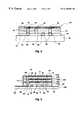
- FIGS. 1A, 1 B and 1 Can exemplary silicon die 10 is depicted. It should be understood that fabrication of the present invention will normally be effected at least partially at the wafer level, and that reference to a single die is for descriptive purposes only, and not limiting of the applicability of the invention to such a structure.
- FIG. 1Adepicts die 10 in an essentially pristine state, being modified only by the addition of conductive exemplary vias 12 and 14 , extending from what will become the front side or active side 16 of die 10 to the back side 18 thereof.
- Vias 12 and 14may be formed by any process known in the art. However, it is preferred and significant to the invention that the vias be formed in situ in the silicon matrix of the die without prior physical removal of the die material.
- viasmay be formed by gravitationally-induced diffusion of metal applied (as by doping) through apertures in a mask or other protective layer on active side 16 .
- exemplary diffusible metals possessing suitable conductivity and without undue resistivityinclude, by way of example, Au and Al.
- Other suitable metalsare known in the art.
- One limitation to the utility of diffusion-forming viasis significant lateral migration of the diffusing metal, which may be somewhat limiting as far as via density due to spacing requirements.
- Vertical diffusion speedmay be enhanced and lateral migration reduced through selective electrochemical anodization of the die using a masking technique as referenced in the aforementioned U.S. Pat. No. 5,455,455 and described in detail in U.S. Pat. No.
- epitaxial layer 20can be formed on active side 16 if active devices are to be fabricated over vias 12 on die 10 .
- Active devicessuch as 22 , superimposed on or immediately adjacent via 12 , are then formed by means well known in the art. Active devices may include, by way of example and not limitation, any such devices known in the art such as diodes, transistors, and memory (ROM, PROM, EPROM, EEPROM, bubble, DRAM, SRAM) including subcomponents such as transistors, capacitors and fuses. Active devices may also be fabricated in the original silicon of the die, as known in the art. Passive devices 23 (FIG.
- a viamay serve as a through or relay via
- a bond pad 24 as depicted capping via 14may be formed as well known in the art to provide an electrical path to a higher die in a stack of which die 10 is a part.
- a protective layer 50such as silicon dioxide, doped silicon dioxide (PSG, BPSG), silicon nitride or a polyimide, may be applied over the entire active surface and all components thereon since all electrical connections are made from the back of the die.
- die 10includes back side terminal structures 26 and 28 for connection to bond pads 24 on the top of a lower die of a stack or for connection to traces, 32 of carrier substrate 30 .
- Terminal structuresmay comprise applied metalization in the form of bond pads 34 .
- a selected depth 19 of the back side 18 of die 10may be selectively etched after being masked, as known in the art, to cause vias 12 and 14 to project downwardly from back side 18 , as shown, and provide enhanced clearance between die 10 and the next lower die in the stack, or between die 10 and carrier substrate 30 .
- C 4 or similar flip-chip style conductive bumps or protrusions 36may be formed directly under a via.
- back side 18may be provided with metalization in the form of circuit traces 38 , which re-pattern some or all of the external electrical connections of the die 10 or of the entire die stack as required by the substrate input/output or I/O pattern, circuit traces 38 thus terminating in conductive bumps or protrusions 36 .
- a non-conductive underfillmay then be introduced between back side 18 and carrier substrate 30 .
- exemplary singulated die 10 ′intended for non-stacked usage, is depicted affixed to a carrier substrate 30 , die 10 ′ being employed alone or in combination with other such dice or dice of other configurations such as in a SIMM or other MCM. Elements as previously identified with regard to FIGS. 1A through 1C are referenced in FIG. 2 by the same numerals.
- Non-conductive protective underfill 40is depicted in FIG. 2 .
- a three-die stack including die 110 a , 110 b and 110 cis depicted assembled and mounted to a carrier substrate 130 .
- Die stack 110is encapsulated, top and sides, by a protective layer 150 such as polyimide or low temperature chemical vapor deposition (CVD) nitride.
- Dies 110 a and 110 bare provided with protective dams 120 projecting downwardly from back sides 18 about the entire die periphery to about the active sides 16 of the next lower die.
- An adhesive or other protective non-conductive filer or sealant 122may be applied between the lower end of each dam 120 and the active side 16 to effect a die-to-die seal and eliminate the need to side-coat the die stack 110 with a protective layer 150 , so that only a protective layer 150 on the top die 110 a is required.
- vias 12 and 14may be placed in any configuration in dice 110 a , 110 b , and 110 c.
- an eight-die stackincluding dice 210 a , 210 b , 210 c , 210 d , 210 e , 210 f , 210 g , and 210 h are depicted mounted on and electrically connected to a carrier substrate 230 .
- a series of common-access via stacks 212 a , 212 b , 212 c , 212 d and 212 eextend vertically through all eight dice and are accessed by each.
- a second series of discrete access via stacks 214 a , 214 b , 214 c , 214 d , 214 e , 214 f , 214 g , and 214 hprovide an individual chipselect function to each die in the stack.
- the total number of required via stacksequals only the number required for common access to the carrier substrate, plus the number required for discrete access (generally equal to the number of dice in the stack).
- exemplary programmable blown or open fuse elements 260 a , 260 b and 260 care also depicted in FIG. 4, such open fuse elements isolating a die above a certain level from a particular via stack.
- a chip-select via for the base dice 210 hmay be isolated from the remaining seven (7) die above it.
- Other viasmay similarly be isolated.
- Programmable antifusesas known in the art, may similarly be employed to selectively connect, rather than disconnect, conductors on and between dice.
- Several programmable activated or closed fuse elementsare depicted at 264 a , 264 b , and 264 c. Fuses and antifuses may, of course, be employed in combination on the same die and on adjacent dice.
- polysilicon or oxide 262located in a via segment (see FIG. 4 ), is a suitable fuse element which may be blown with a high current.
- a thin film 70 of nichrome or titanium-tungstenmay be employed on the active side 16 or back side 18 of a die 10 between a horizontal conductive path 74 and a vertically-extending via 12 or 14 .
- Suitable antifuse technologyis disclosed, by way of example, in U.S. Pat. Nos. 5,110,754 and 5,324,681, the disclosures of which are hereby incorporated by this reference. See also U.S. Pat. Nos. 5,485,031 and 5,485,032.
- fusesmay be blown and antifuses activated or closed on the individual die prior to stacking or after the stack is assembled. It is preferable to qualify known good die (KGD) after the fuses are blown and antifuses closed at die or wafer-level, and then fabricate a KGD stack for assured greater yield of the ultimate, resulting MCM.
- KGDknown good die
- a die on top of a stackmay be configured with antifuse connections to all chip selects of the lower die in the stack. With such an arrangement, if a die of the stack fails during burn-in or test, one can then contact the upper die with probes or through electrical programming and activate or close the antifuses to “add” the top die to the circuit to replace the defective lower die. Standard fuse methodology is used to “remove” the bad die from the circuit. A known good die is preferably employed as the top die in the stack.
- a lowermost diemay be used to laterally reroute the via pattern from one designed to best accommodate the sizes, configurations and various placements of components on the die above to a standardized or other selective pattern on a carrier substrate.
- Rerouting conductorsmay be formed on the upper side of the rerouting die to contact terminals on the back side of the next-uppermost die. The rerouting conductors would then extend to vias in the rerouting die for connection to traces on the carrier.
- dice of different size and shapemay be stacked, as long as the vias vertically electrically connecting them are aligned. It is further contemplated that the invention has utility in paralleling processors by stacking the processors. In such a case, there would be additional pin types connected, such as clock inputs/outputs, etc., as well known in the art.
Landscapes
- Engineering & Computer Science (AREA)
- Microelectronics & Electronic Packaging (AREA)
- Power Engineering (AREA)
- Computer Hardware Design (AREA)
- Physics & Mathematics (AREA)
- Condensed Matter Physics & Semiconductors (AREA)
- General Physics & Mathematics (AREA)
- Design And Manufacture Of Integrated Circuits (AREA)
- Semiconductor Integrated Circuits (AREA)
Abstract
Description
Claims (33)
Priority Applications (2)
| Application Number | Priority Date | Filing Date | Title |
|---|---|---|---|
| US08/909,785US6168969B1 (en) | 1996-02-16 | 1997-08-12 | Surface mount IC using silicon vias in an area array format or same size as die array |
| US09/645,905US6400008B1 (en) | 1996-02-16 | 2000-08-25 | Surface mount ic using silicon vias in an area array format or same size as die array |
Applications Claiming Priority (2)
| Application Number | Priority Date | Filing Date | Title |
|---|---|---|---|
| US08/601,302US5973396A (en) | 1996-02-16 | 1996-02-16 | Surface mount IC using silicon vias in an area array format or same size as die array |
| US08/909,785US6168969B1 (en) | 1996-02-16 | 1997-08-12 | Surface mount IC using silicon vias in an area array format or same size as die array |
Related Parent Applications (1)
| Application Number | Title | Priority Date | Filing Date |
|---|---|---|---|
| US08/601,302DivisionUS5973396A (en) | 1996-02-16 | 1996-02-16 | Surface mount IC using silicon vias in an area array format or same size as die array |
Related Child Applications (1)
| Application Number | Title | Priority Date | Filing Date |
|---|---|---|---|
| US09/645,905ContinuationUS6400008B1 (en) | 1996-02-16 | 2000-08-25 | Surface mount ic using silicon vias in an area array format or same size as die array |
Publications (1)
| Publication Number | Publication Date |
|---|---|
| US6168969B1true US6168969B1 (en) | 2001-01-02 |
Family
ID=24407002
Family Applications (3)
| Application Number | Title | Priority Date | Filing Date |
|---|---|---|---|
| US08/601,302Expired - LifetimeUS5973396A (en) | 1996-02-16 | 1996-02-16 | Surface mount IC using silicon vias in an area array format or same size as die array |
| US08/909,785Expired - LifetimeUS6168969B1 (en) | 1996-02-16 | 1997-08-12 | Surface mount IC using silicon vias in an area array format or same size as die array |
| US09/645,905Expired - LifetimeUS6400008B1 (en) | 1996-02-16 | 2000-08-25 | Surface mount ic using silicon vias in an area array format or same size as die array |
Family Applications Before (1)
| Application Number | Title | Priority Date | Filing Date |
|---|---|---|---|
| US08/601,302Expired - LifetimeUS5973396A (en) | 1996-02-16 | 1996-02-16 | Surface mount IC using silicon vias in an area array format or same size as die array |
Family Applications After (1)
| Application Number | Title | Priority Date | Filing Date |
|---|---|---|---|
| US09/645,905Expired - LifetimeUS6400008B1 (en) | 1996-02-16 | 2000-08-25 | Surface mount ic using silicon vias in an area array format or same size as die array |
Country Status (1)
| Country | Link |
|---|---|
| US (3) | US5973396A (en) |
Cited By (50)
| Publication number | Priority date | Publication date | Assignee | Title |
|---|---|---|---|---|
| US6429509B1 (en)* | 1999-05-03 | 2002-08-06 | United Microelectronics Corporation | Integrated circuit with improved interconnect structure and process for making same |
| US6502231B1 (en) | 2001-05-31 | 2002-12-31 | Applied Micro Circuits Corporation | Integrated circuit template cell system and method |
| EP1280203A3 (en)* | 2001-07-27 | 2003-03-26 | Nokia Corporation | 3D-Semiconductor Package |
| US20040021139A1 (en)* | 2002-07-31 | 2004-02-05 | Jackson Timothy L. | Semiconductor dice having backside redistribution layer accessed using through-silicon vias, methods of fabrication and assemblies |
| US20040023436A1 (en)* | 2001-09-17 | 2004-02-05 | Megic Corporation | Structure of high performance combo chip and processing method |
| WO2003050850A3 (en)* | 2001-12-12 | 2004-03-11 | Infineon Technologies Ag | Contacting of a semiconductor chip on a substrate using flip-chip-like technology |
| US6849480B1 (en)* | 1999-05-07 | 2005-02-01 | Seagate Technology Llc | Surface mount IC stacking method and device |
| US20050067714A1 (en)* | 2003-09-30 | 2005-03-31 | Rumer Christopher L. | Method and apparatus for a dual substrate package |
| DE10345464A1 (en)* | 2003-09-30 | 2005-05-04 | Infineon Technologies Ag | Multi-chip housing has carrier substrate with terminal line regions for connecting semiconductor chip metallization contacts with printed circuit board contact surfaces acting as encapsulation housing |
| US20050110159A1 (en)* | 2003-11-21 | 2005-05-26 | Chang-Woo Oh | Stacked integrated circuit device including multiple substrates and method of manufacturing the same |
| US20050218526A1 (en)* | 2004-03-25 | 2005-10-06 | Sanyo Electric Co., Ltd. | Semiconductor device |
| US6982487B2 (en) | 2003-03-25 | 2006-01-03 | Samsung Electronics Co., Ltd. | Wafer level package and multi-package stack |
| US20060043569A1 (en)* | 2004-08-27 | 2006-03-02 | Benson Peter A | Low temperature methods of forming back side redistribution layers in association with through wafer interconnects, semiconductor devices including same, and assemblies |
| US20060071342A1 (en)* | 2004-09-29 | 2006-04-06 | Sanyo Electric Co., Ltd. | Semiconductor device manufacturing method of the same |
| US7030466B1 (en) | 1999-05-03 | 2006-04-18 | United Microelectronics Corporation | Intermediate structure for making integrated circuit device and wafer |
| US20060199365A1 (en)* | 2005-03-02 | 2006-09-07 | Endevco Corporation | Junction-isolated vias |
| US7179740B1 (en) | 1999-05-03 | 2007-02-20 | United Microelectronics Corporation | Integrated circuit with improved interconnect structure and process for making same |
| US20070042562A1 (en)* | 1998-02-06 | 2007-02-22 | Tessera Technologies Hungary Kft. | Integrated circuit device |
| US20070051072A1 (en)* | 2005-09-06 | 2007-03-08 | Joseph Lai | Pills on tape and reel |
| US20070172983A1 (en)* | 2006-01-25 | 2007-07-26 | Min-Lung Huang | Three-dimensional package and method of making the same |
| US20070172986A1 (en)* | 2006-01-25 | 2007-07-26 | Min-Lung Huang | Three-dimensional package and method of making the same |
| US20090115026A1 (en)* | 2007-11-05 | 2009-05-07 | Texas Instruments Incorporated | Semiconductor device having through-silicon vias for high current,high frequency, and heat dissipation |
| US20090278245A1 (en)* | 2008-05-12 | 2009-11-12 | Texas Instruments Inc | Packaged electronic devices with face-up die having tsv connection to leads and die pad |
| US20090305502A1 (en)* | 2008-06-10 | 2009-12-10 | Ho-Jin Lee | Methods of Forming Integrated Circuit Chips Having Vertically Extended Through-Substrate Vias Therein and Chips Formed Thereby |
| EP1472730A4 (en)* | 2002-01-16 | 2010-04-14 | Mann Alfred E Found Scient Res | HOUSING FOR ELECTRONIC CIRCUITS WITH REDUCED SIZE |
| US20100117209A1 (en)* | 2007-02-28 | 2010-05-13 | Bezama Raschid J | Multiple chips on a semiconductor chip with cooling means |
| US7723213B2 (en)* | 2006-11-02 | 2010-05-25 | Oki Semiconductor Co., Ltd. | Manufacturing method of semiconductor chips and semiconductor device having the semiconductor chips |
| US20100155940A1 (en)* | 2008-12-19 | 2010-06-24 | Renesas Technology Corp. | Semiconductor device and method of manufacturing the same |
| US20100182041A1 (en)* | 2009-01-22 | 2010-07-22 | International Business Machines Corporation | 3d chip-stack with fuse-type through silicon via |
| US7843072B1 (en) | 2008-08-12 | 2010-11-30 | Amkor Technology, Inc. | Semiconductor package having through holes |
| US7843052B1 (en) | 2008-11-13 | 2010-11-30 | Amkor Technology, Inc. | Semiconductor devices and fabrication methods thereof |
| US7973629B2 (en) | 2001-09-04 | 2011-07-05 | Megica Corporation | Method for making high-performance RF integrated circuits |
| US20120112312A1 (en)* | 2010-11-04 | 2012-05-10 | Qualcomm Incorporated | Integrated Circuit Chip Customization Using Backside Access |
| US8324511B1 (en) | 2010-04-06 | 2012-12-04 | Amkor Technology, Inc. | Through via nub reveal method and structure |
| US8390130B1 (en) | 2011-01-06 | 2013-03-05 | Amkor Technology, Inc. | Through via recessed reveal structure and method |
| US8440554B1 (en) | 2010-08-02 | 2013-05-14 | Amkor Technology, Inc. | Through via connected backside embedded circuit features structure and method |
| US8487445B1 (en) | 2010-10-05 | 2013-07-16 | Amkor Technology, Inc. | Semiconductor device having through electrodes protruding from dielectric layer |
| US8552548B1 (en) | 2011-11-29 | 2013-10-08 | Amkor Technology, Inc. | Conductive pad on protruding through electrode semiconductor device |
| US8791501B1 (en)* | 2010-12-03 | 2014-07-29 | Amkor Technology, Inc. | Integrated passive device structure and method |
| US20140369148A1 (en)* | 2003-04-21 | 2014-12-18 | Ps4 Luxco S.A.R.L. | Memory module and memory system |
| EP2741426A4 (en)* | 2011-08-01 | 2015-05-06 | Murata Manufacturing Co | High-frequency module |
| US9048298B1 (en) | 2012-03-29 | 2015-06-02 | Amkor Technology, Inc. | Backside warpage control structure and fabrication method |
| US9129943B1 (en) | 2012-03-29 | 2015-09-08 | Amkor Technology, Inc. | Embedded component package and fabrication method |
| US9425098B2 (en) | 2012-09-07 | 2016-08-23 | Mediatek Inc. | Radio-frequency device package and method for fabricating the same |
| US9760212B2 (en) | 2013-09-30 | 2017-09-12 | Synaptics Incorported | Matrix sensor for image touch sensing |
| US10042489B2 (en) | 2013-09-30 | 2018-08-07 | Synaptics Incorporated | Matrix sensor for image touch sensing |
| US10042488B2 (en) | 2014-04-04 | 2018-08-07 | Synaptics Incorporated | Through silicon vias for backside connection |
| US10067587B2 (en) | 2015-12-29 | 2018-09-04 | Synaptics Incorporated | Routing conductors in an integrated display device and sensing device |
| US10806026B2 (en)* | 2018-07-12 | 2020-10-13 | International Business Machines Corporation | Modified PCB vias to prevent burn events |
| US10811341B2 (en) | 2009-01-05 | 2020-10-20 | Amkor Technology Singapore Holding Pte Ltd. | Semiconductor device with through-mold via |
Families Citing this family (119)
| Publication number | Priority date | Publication date | Assignee | Title |
|---|---|---|---|---|
| US5973396A (en)* | 1996-02-16 | 1999-10-26 | Micron Technology, Inc. | Surface mount IC using silicon vias in an area array format or same size as die array |
| US6809421B1 (en)* | 1996-12-02 | 2004-10-26 | Kabushiki Kaisha Toshiba | Multichip semiconductor device, chip therefor and method of formation thereof |
| JPH10275966A (en)* | 1997-01-30 | 1998-10-13 | Ibiden Co Ltd | Printed-wiring board and its manufacture |
| US20060081971A1 (en)* | 1997-09-30 | 2006-04-20 | Jeng Jye Shau | Signal transfer methods for integrated circuits |
| US20020157082A1 (en)* | 1997-09-30 | 2002-10-24 | Jeng-Jye Shau | Inter-dice wafer level signal transfer methods for integrated circuits |
| US7786562B2 (en)* | 1997-11-11 | 2010-08-31 | Volkan Ozguz | Stackable semiconductor chip layer comprising prefabricated trench interconnect vias |
| US20040113222A1 (en)* | 2002-09-16 | 2004-06-17 | Ozguz Volkan H | Stacked microelectronic module with vertical interconnect vias |
| JP3147087B2 (en)* | 1998-06-17 | 2001-03-19 | 日本電気株式会社 | Stacked semiconductor device heat dissipation structure |
| RU2134466C1 (en)* | 1998-12-08 | 1999-08-10 | Таран Александр Иванович | Carrier of crystal of integrated circuit |
| US6248961B1 (en)* | 1998-12-15 | 2001-06-19 | International Business Machines Corporation | Wave solder application for ball grid array modules and solder plug |
| JP2000243900A (en)* | 1999-02-23 | 2000-09-08 | Rohm Co Ltd | Semiconductor chip, semiconductor device using it, and manufacture of semiconductor chip |
| DE19916572A1 (en)* | 1999-04-13 | 2000-10-26 | Siemens Ag | Optical semiconductor component with transparent protection layer |
| DE19983953T1 (en)* | 1999-05-07 | 2002-06-20 | Seagate Technology Llc | Method and device for stacking surface mount ICs |
| DE19928733A1 (en) | 1999-06-23 | 2001-01-04 | Giesecke & Devrient Gmbh | Semiconductor memory chip module |
| US6753638B2 (en) | 2000-02-03 | 2004-06-22 | Calient Networks, Inc. | Electrostatic actuator for micromechanical systems |
| US6710454B1 (en) | 2000-02-16 | 2004-03-23 | Micron Technology, Inc. | Adhesive layer for an electronic apparatus having multiple semiconductor devices |
| US6535396B1 (en)* | 2000-04-28 | 2003-03-18 | Delphi Technologies, Inc. | Combination circuit board and segmented conductive bus substrate |
| US6576494B1 (en) | 2000-06-28 | 2003-06-10 | Micron Technology, Inc. | Recessed encapsulated microelectronic devices and methods for formation |
| US7271491B1 (en)* | 2000-08-31 | 2007-09-18 | Micron Technology, Inc. | Carrier for wafer-scale package and wafer-scale package including the carrier |
| US6589594B1 (en)* | 2000-08-31 | 2003-07-08 | Micron Technology, Inc. | Method for filling a wafer through-via with a conductive material |
| DE10044148A1 (en)* | 2000-09-06 | 2002-03-21 | Infineon Technologies Ag | Electronic component with stacked components and process for its manufacture |
| US6674161B1 (en)* | 2000-10-03 | 2004-01-06 | Rambus Inc. | Semiconductor stacked die devices |
| US6506981B1 (en)* | 2000-11-22 | 2003-01-14 | Janusz B. Liberkowski | Interconnect structure having fuse or anti-fuse links between profiled apertures |
| JP4422323B2 (en)* | 2000-12-15 | 2010-02-24 | 株式会社ルネサステクノロジ | Semiconductor device |
| US20020074633A1 (en)* | 2000-12-18 | 2002-06-20 | Larson Lary R. | Interconnection of active and passive components in substrate |
| KR100364635B1 (en)* | 2001-02-09 | 2002-12-16 | 삼성전자 주식회사 | Chip-Level Three-Dimensional Multi-Chip Package Having Chip Selection Pad Formed On Chip-Level And Making Method Therefor |
| DE10126610B4 (en)* | 2001-05-31 | 2007-11-29 | Infineon Technologies Ag | Memory module and method for testing a semiconductor chip |
| SG111919A1 (en) | 2001-08-29 | 2005-06-29 | Micron Technology Inc | Packaged microelectronic devices and methods of forming same |
| US6580144B2 (en)* | 2001-09-28 | 2003-06-17 | Hewlett-Packard Development Company, L.P. | One time programmable fuse/anti-fuse combination based memory cell |
| US6963493B2 (en)* | 2001-11-08 | 2005-11-08 | Avx Corporation | Multilayer electronic devices with via components |
| US6635572B1 (en)* | 2001-11-28 | 2003-10-21 | Advanced Micro Devices, Inc. | Method of substrate silicon removal for integrated circuit devices |
| US7109571B1 (en) | 2001-12-03 | 2006-09-19 | National Semiconductor Corporation | Method of forming a hermetic seal for silicon die with metal feed through structure |
| US6677235B1 (en)* | 2001-12-03 | 2004-01-13 | National Semiconductor Corporation | Silicon die with metal feed through structure |
| US6599778B2 (en)* | 2001-12-19 | 2003-07-29 | International Business Machines Corporation | Chip and wafer integration process using vertical connections |
| US6762076B2 (en)* | 2002-02-20 | 2004-07-13 | Intel Corporation | Process of vertically stacking multiple wafers supporting different active integrated circuit (IC) devices |
| US6594171B1 (en) | 2002-03-07 | 2003-07-15 | Hewlett-Packard Development Company, L.P. | Memory systems and methods of making the same |
| US7728339B1 (en) | 2002-05-03 | 2010-06-01 | Calient Networks, Inc. | Boundary isolation for microelectromechanical devices |
| SG120879A1 (en) | 2002-08-08 | 2006-04-26 | Micron Technology Inc | Packaged microelectronic components |
| TWI227050B (en)* | 2002-10-11 | 2005-01-21 | Sanyo Electric Co | Semiconductor device and method for manufacturing the same |
| US20040088855A1 (en)* | 2002-11-11 | 2004-05-13 | Salman Akram | Interposers for chip-scale packages, chip-scale packages including the interposers, test apparatus for effecting wafer-level testing of the chip-scale packages, and methods |
| SG114585A1 (en) | 2002-11-22 | 2005-09-28 | Micron Technology Inc | Packaged microelectronic component assemblies |
| TW569416B (en)* | 2002-12-19 | 2004-01-01 | Via Tech Inc | High density multi-chip module structure and manufacturing method thereof |
| US6853064B2 (en) | 2003-05-12 | 2005-02-08 | Micron Technology, Inc. | Semiconductor component having stacked, encapsulated dice |
| DE60323883D1 (en)* | 2003-05-28 | 2008-11-13 | Infineon Technologies Ag | Ic-gehäuse mit flexiblem substrat |
| US7368810B2 (en) | 2003-08-29 | 2008-05-06 | Micron Technology, Inc. | Invertible microfeature device packages |
| US6947306B2 (en)* | 2003-09-30 | 2005-09-20 | Infineon Technologies Ag | Backside of chip implementation of redundancy fuses and contact pads |
| US20050104027A1 (en)* | 2003-10-17 | 2005-05-19 | Lazarev Pavel I. | Three-dimensional integrated circuit with integrated heat sinks |
| JP4377269B2 (en)* | 2004-03-19 | 2009-12-02 | Necエレクトロニクス株式会社 | Semiconductor device |
| TWI272683B (en)* | 2004-05-24 | 2007-02-01 | Sanyo Electric Co | Semiconductor device and manufacturing method thereof |
| WO2006024009A2 (en)* | 2004-08-24 | 2006-03-02 | C-Core Technologies, Inc. | Edge plated printed wiring boards |
| US7491582B2 (en)* | 2004-08-31 | 2009-02-17 | Seiko Epson Corporation | Method for manufacturing semiconductor device and semiconductor device |
| US7400047B2 (en)* | 2004-12-13 | 2008-07-15 | Agere Systems Inc. | Integrated circuit with stacked-die configuration utilizing substrate conduction |
| US7317256B2 (en)* | 2005-06-01 | 2008-01-08 | Intel Corporation | Electronic packaging including die with through silicon via |
| JP4311376B2 (en) | 2005-06-08 | 2009-08-12 | セイコーエプソン株式会社 | Semiconductor device, semiconductor device manufacturing method, electronic component, circuit board, and electronic apparatus |
| US7838997B2 (en) | 2005-06-14 | 2010-11-23 | John Trezza | Remote chip attachment |
| US7786592B2 (en) | 2005-06-14 | 2010-08-31 | John Trezza | Chip capacitive coupling |
| US8456015B2 (en) | 2005-06-14 | 2013-06-04 | Cufer Asset Ltd. L.L.C. | Triaxial through-chip connection |
| US7687400B2 (en) | 2005-06-14 | 2010-03-30 | John Trezza | Side stacking apparatus and method |
| US7781886B2 (en) | 2005-06-14 | 2010-08-24 | John Trezza | Electronic chip contact structure |
| US7767493B2 (en) | 2005-06-14 | 2010-08-03 | John Trezza | Post & penetration interconnection |
| US7534722B2 (en) | 2005-06-14 | 2009-05-19 | John Trezza | Back-to-front via process |
| US7989958B2 (en) | 2005-06-14 | 2011-08-02 | Cufer Assett Ltd. L.L.C. | Patterned contact |
| US7560813B2 (en) | 2005-06-14 | 2009-07-14 | John Trezza | Chip-based thermo-stack |
| US7521806B2 (en)* | 2005-06-14 | 2009-04-21 | John Trezza | Chip spanning connection |
| US7851348B2 (en) | 2005-06-14 | 2010-12-14 | Abhay Misra | Routingless chip architecture |
| KR100721353B1 (en)* | 2005-07-08 | 2007-05-25 | 삼성전자주식회사 | Structure and Manufacturing Method of Chip Insert Intermediate Substrate, Wafer Level Stacking Structure and Package Structure of Heterogeneous Chip |
| US7327592B2 (en) | 2005-08-30 | 2008-02-05 | Micron Technology, Inc. | Self-identifying stacked die semiconductor components |
| US7352602B2 (en)* | 2005-12-30 | 2008-04-01 | Micron Technology, Inc. | Configurable inputs and outputs for memory stacking system and method |
| SG135074A1 (en) | 2006-02-28 | 2007-09-28 | Micron Technology Inc | Microelectronic devices, stacked microelectronic devices, and methods for manufacturing such devices |
| JP4661642B2 (en)* | 2006-03-13 | 2011-03-30 | セイコーエプソン株式会社 | Semiconductor device, ink cartridge, and electronic device |
| US7613009B2 (en)* | 2006-03-15 | 2009-11-03 | Tdk Corporation | Electrical transition for an RF component |
| US7898095B2 (en)* | 2006-03-20 | 2011-03-01 | Tezzaron Semiconductor, Inc. | Fiducial scheme adapted for stacked integrated circuits |
| US7514289B2 (en)* | 2006-03-20 | 2009-04-07 | Sun Microsystems, Inc. | Methods and structures for facilitating proximity communication |
| US7687397B2 (en) | 2006-06-06 | 2010-03-30 | John Trezza | Front-end processed wafer having through-chip connections |
| US7385283B2 (en)* | 2006-06-27 | 2008-06-10 | Taiwan Semiconductor Manufacturing Co., Ltd. | Three dimensional integrated circuit and method of making the same |
| US7446424B2 (en)* | 2006-07-19 | 2008-11-04 | Taiwan Semiconductor Manufacturing Co., Ltd. | Interconnect structure for semiconductor package |
| US7473577B2 (en)* | 2006-08-11 | 2009-01-06 | International Business Machines Corporation | Integrated chip carrier with compliant interconnect |
| EP1906441A1 (en)* | 2006-09-29 | 2008-04-02 | Schott Advanced Packaging Singapore Pte. Ldt. | Wafer with semiconductor devices and method of manufacturing the same |
| JP5269799B2 (en)* | 2006-10-17 | 2013-08-21 | キューファー アセット リミテッド. エル.エル.シー. | Wafer via formation |
| US7670874B2 (en) | 2007-02-16 | 2010-03-02 | John Trezza | Plated pillar package formation |
| US8198716B2 (en)* | 2007-03-26 | 2012-06-12 | Intel Corporation | Die backside wire bond technology for single or stacked die package |
| US7638869B2 (en)* | 2007-03-28 | 2009-12-29 | Qimonda Ag | Semiconductor device |
| US7748116B2 (en)* | 2007-04-05 | 2010-07-06 | John Trezza | Mobile binding in an electronic connection |
| US7850060B2 (en)* | 2007-04-05 | 2010-12-14 | John Trezza | Heat cycle-able connection |
| US20080261392A1 (en)* | 2007-04-23 | 2008-10-23 | John Trezza | Conductive via formation |
| US7960210B2 (en)* | 2007-04-23 | 2011-06-14 | Cufer Asset Ltd. L.L.C. | Ultra-thin chip packaging |
| US7902638B2 (en)* | 2007-05-04 | 2011-03-08 | Stats Chippac, Ltd. | Semiconductor die with through-hole via on saw streets and through-hole via in active area of die |
| US8110930B2 (en)* | 2007-06-19 | 2012-02-07 | Intel Corporation | Die backside metallization and surface activated bonding for stacked die packages |
| KR101452548B1 (en)* | 2007-06-20 | 2014-10-21 | 스카이워크스 솔루션즈, 인코포레이티드 | Semiconductor die with backside passive device integration |
| US20090045444A1 (en)* | 2007-08-13 | 2009-02-19 | Holger Huebner | Integrated device and circuit system |
| US20090057867A1 (en)* | 2007-08-30 | 2009-03-05 | Vincent Hool | Integrated Circuit Package with Passive Component |
| US8044497B2 (en)* | 2007-09-10 | 2011-10-25 | Intel Corporation | Stacked die package |
| US9955582B2 (en)* | 2008-04-23 | 2018-04-24 | Skyworks Solutions, Inc. | 3-D stacking of active devices over passive devices |
| KR100994978B1 (en) | 2008-07-23 | 2010-11-18 | (주) 이피웍스 | Three-dimensional semiconductor device, manufacturing method thereof, and electrical interruption method using fuse pattern of three-dimensional semiconductor device |
| US7872332B2 (en)* | 2008-09-11 | 2011-01-18 | Micron Technology, Inc. | Interconnect structures for stacked dies, including penetrating structures for through-silicon vias, and associated systems and methods |
| US8803330B2 (en)* | 2008-09-27 | 2014-08-12 | Stats Chippac Ltd. | Integrated circuit package system with mounting structure |
| US7939926B2 (en)* | 2008-12-12 | 2011-05-10 | Qualcomm Incorporated | Via first plus via last technique for IC interconnects |
| US7839163B2 (en)* | 2009-01-22 | 2010-11-23 | International Business Machines Corporation | Programmable through silicon via |
| JP5568170B2 (en)* | 2009-02-23 | 2014-08-06 | 新光電気工業株式会社 | Wiring board and manufacturing method thereof |
| JP5367616B2 (en)* | 2009-02-23 | 2013-12-11 | 新光電気工業株式会社 | Wiring board and manufacturing method thereof |
| US20100237481A1 (en)* | 2009-03-20 | 2010-09-23 | Chi Heejo | Integrated circuit packaging system with dual sided connection and method of manufacture thereof |
| US7989282B2 (en)* | 2009-03-26 | 2011-08-02 | International Business Machines Corporation | Structure and method for latchup improvement using through wafer via latchup guard ring |
| US8232625B2 (en)* | 2009-03-26 | 2012-07-31 | International Business Machines Corporation | ESD network circuit with a through wafer via structure and a method of manufacture |
| US7923290B2 (en) | 2009-03-27 | 2011-04-12 | Stats Chippac Ltd. | Integrated circuit packaging system having dual sided connection and method of manufacture thereof |
| US8319325B2 (en)* | 2009-06-12 | 2012-11-27 | Qualcomm Incorporated | Intra-die routing using back side redistribution layer and associated method |
| US8054597B2 (en)* | 2009-06-23 | 2011-11-08 | International Business Machines Corporation | Electrostatic discharge structures and methods of manufacture |
| US8304863B2 (en) | 2010-02-09 | 2012-11-06 | International Business Machines Corporation | Electromigration immune through-substrate vias |
| US8426961B2 (en)* | 2010-06-25 | 2013-04-23 | Taiwan Semiconductor Manufacturing Company, Ltd. | Embedded 3D interposer structure |
| US20120025930A1 (en)* | 2010-07-30 | 2012-02-02 | International Business Machines Corporation | Programmable antifuse matrix for module decoupling |
| US9070851B2 (en) | 2010-09-24 | 2015-06-30 | Seoul Semiconductor Co., Ltd. | Wafer-level light emitting diode package and method of fabricating the same |
| US8218347B1 (en) | 2010-10-12 | 2012-07-10 | Apple Inc. | Stacked memory device having a scalable bandwidth interface |
| US9726818B1 (en) | 2013-05-30 | 2017-08-08 | Hrl Laboratories, Llc | Multi-wavelength band optical phase and amplitude controller |
| US9515006B2 (en) | 2013-09-27 | 2016-12-06 | Freescale Semiconductor, Inc. | 3D device packaging using through-substrate posts |
| US9508702B2 (en) | 2013-09-27 | 2016-11-29 | Freescale Semiconductor, Inc. | 3D device packaging using through-substrate posts |
| US9508701B2 (en)* | 2013-09-27 | 2016-11-29 | Freescale Semiconductor, Inc. | 3D device packaging using through-substrate pillars |
| US9332632B2 (en) | 2014-08-20 | 2016-05-03 | Stablcor Technology, Inc. | Graphene-based thermal management cores and systems and methods for constructing printed wiring boards |
| CN205944139U (en) | 2016-03-30 | 2017-02-08 | 首尔伟傲世有限公司 | Ultraviolet ray light -emitting diode spare and contain this emitting diode module |
| US10991670B2 (en)* | 2018-09-28 | 2021-04-27 | Semiconductor Components Industries, Llc | Semiconductor device assemblies including spacer with embedded semiconductor die |
| US12103843B2 (en) | 2021-01-20 | 2024-10-01 | Calient.Ai Inc. | MEMS mirror arrays with reduced crosstalk |
Citations (15)
| Publication number | Priority date | Publication date | Assignee | Title |
|---|---|---|---|---|
| US3761782A (en) | 1971-05-19 | 1973-09-25 | Signetics Corp | Semiconductor structure, assembly and method |
| US3947840A (en) | 1974-08-16 | 1976-03-30 | Monsanto Company | Integrated semiconductor light-emitting display array |
| US4499655A (en) | 1981-03-18 | 1985-02-19 | General Electric Company | Method for making alignment-enhancing feed-through conductors for stackable silicon-on-sapphire |
| US5229647A (en) | 1991-03-27 | 1993-07-20 | Micron Technology, Inc. | High density data storage using stacked wafers |
| US5378927A (en) | 1993-05-24 | 1995-01-03 | International Business Machines Corporation | Thin-film wiring layout for a non-planar thin-film structure |
| US5406125A (en) | 1993-04-15 | 1995-04-11 | Martin Marietta Corp. | Semiconductor device having a metalized via hole |
| US5455445A (en)* | 1994-01-21 | 1995-10-03 | Kulite Semiconductor Products, Inc. | Multi-level semiconductor structures having environmentally isolated elements |
| US5510655A (en) | 1990-11-26 | 1996-04-23 | The Boeing Company | Silicon wafers containing conductive feedthroughs |
| US5528080A (en) | 1993-03-05 | 1996-06-18 | Goldstein; Edward F. | Electrically conductive interconnection through a body of semiconductor material |
| US5552338A (en)* | 1994-09-26 | 1996-09-03 | Intel Corporation | Method of using latchup current to blow a fuse in an integrated circuit |
| US5552633A (en) | 1995-06-06 | 1996-09-03 | Martin Marietta Corporation | Three-dimensional multimodule HDI arrays with heat spreading |
| US5608264A (en) | 1995-06-05 | 1997-03-04 | Harris Corporation | Surface mountable integrated circuit with conductive vias |
| US5623160A (en)* | 1995-09-14 | 1997-04-22 | Liberkowski; Janusz B. | Signal-routing or interconnect substrate, structure and apparatus |
| US5675180A (en) | 1994-06-23 | 1997-10-07 | Cubic Memory, Inc. | Vertical interconnect process for silicon segments |
| US5682062A (en) | 1995-06-05 | 1997-10-28 | Harris Corporation | System for interconnecting stacked integrated circuits |
Family Cites Families (12)
| Publication number | Priority date | Publication date | Assignee | Title |
|---|---|---|---|---|
| US4764846A (en)* | 1987-01-05 | 1988-08-16 | Irvine Sensors Corporation | High density electronic package comprising stacked sub-modules |
| US4983533A (en)* | 1987-10-28 | 1991-01-08 | Irvine Sensors Corporation | High-density electronic modules - process and product |
| US4972248A (en)* | 1989-05-11 | 1990-11-20 | Syracuse University | Multi-layer circuit structure with thin semiconductor channels |
| JP3547146B2 (en)* | 1991-06-10 | 2004-07-28 | 日本特殊陶業株式会社 | Package for integrated circuit |
| US5128831A (en)* | 1991-10-31 | 1992-07-07 | Micron Technology, Inc. | High-density electronic package comprising stacked sub-modules which are electrically interconnected by solder-filled vias |
| US5266833A (en)* | 1992-03-30 | 1993-11-30 | Capps David F | Integrated circuit bus structure |
| US5298767A (en)* | 1992-10-06 | 1994-03-29 | Kulite Semiconductor Products, Inc. | Porous silicon carbide (SiC) semiconductor device |
| US5386142A (en)* | 1993-05-07 | 1995-01-31 | Kulite Semiconductor Products, Inc. | Semiconductor structures having environmentally isolated elements and method for making the same |
| US5380681A (en)* | 1994-03-21 | 1995-01-10 | United Microelectronics Corporation | Three-dimensional multichip package and methods of fabricating |
| US5481134A (en)* | 1994-05-03 | 1996-01-02 | Hughes Aircraft Company | Stacked high density interconnected integrated circuit system |
| US5434745A (en)* | 1994-07-26 | 1995-07-18 | White Microelectronics Div. Of Bowmar Instrument Corp. | Stacked silicon die carrier assembly |
| US5973396A (en)* | 1996-02-16 | 1999-10-26 | Micron Technology, Inc. | Surface mount IC using silicon vias in an area array format or same size as die array |
- 1996
- 1996-02-16USUS08/601,302patent/US5973396A/ennot_activeExpired - Lifetime
- 1997
- 1997-08-12USUS08/909,785patent/US6168969B1/ennot_activeExpired - Lifetime
- 2000
- 2000-08-25USUS09/645,905patent/US6400008B1/ennot_activeExpired - Lifetime
Patent Citations (15)
| Publication number | Priority date | Publication date | Assignee | Title |
|---|---|---|---|---|
| US3761782A (en) | 1971-05-19 | 1973-09-25 | Signetics Corp | Semiconductor structure, assembly and method |
| US3947840A (en) | 1974-08-16 | 1976-03-30 | Monsanto Company | Integrated semiconductor light-emitting display array |
| US4499655A (en) | 1981-03-18 | 1985-02-19 | General Electric Company | Method for making alignment-enhancing feed-through conductors for stackable silicon-on-sapphire |
| US5510655A (en) | 1990-11-26 | 1996-04-23 | The Boeing Company | Silicon wafers containing conductive feedthroughs |
| US5229647A (en) | 1991-03-27 | 1993-07-20 | Micron Technology, Inc. | High density data storage using stacked wafers |
| US5528080A (en) | 1993-03-05 | 1996-06-18 | Goldstein; Edward F. | Electrically conductive interconnection through a body of semiconductor material |
| US5406125A (en) | 1993-04-15 | 1995-04-11 | Martin Marietta Corp. | Semiconductor device having a metalized via hole |
| US5378927A (en) | 1993-05-24 | 1995-01-03 | International Business Machines Corporation | Thin-film wiring layout for a non-planar thin-film structure |
| US5455445A (en)* | 1994-01-21 | 1995-10-03 | Kulite Semiconductor Products, Inc. | Multi-level semiconductor structures having environmentally isolated elements |
| US5675180A (en) | 1994-06-23 | 1997-10-07 | Cubic Memory, Inc. | Vertical interconnect process for silicon segments |
| US5552338A (en)* | 1994-09-26 | 1996-09-03 | Intel Corporation | Method of using latchup current to blow a fuse in an integrated circuit |
| US5608264A (en) | 1995-06-05 | 1997-03-04 | Harris Corporation | Surface mountable integrated circuit with conductive vias |
| US5682062A (en) | 1995-06-05 | 1997-10-28 | Harris Corporation | System for interconnecting stacked integrated circuits |
| US5552633A (en) | 1995-06-06 | 1996-09-03 | Martin Marietta Corporation | Three-dimensional multimodule HDI arrays with heat spreading |
| US5623160A (en)* | 1995-09-14 | 1997-04-22 | Liberkowski; Janusz B. | Signal-routing or interconnect substrate, structure and apparatus |
Cited By (127)
| Publication number | Priority date | Publication date | Assignee | Title |
|---|---|---|---|---|
| US8592831B2 (en) | 1998-02-06 | 2013-11-26 | Invensas Corp. | Integrated circuit device |
| US9530945B2 (en) | 1998-02-06 | 2016-12-27 | Invensas Corporation | Integrated circuit device |
| US20070042562A1 (en)* | 1998-02-06 | 2007-02-22 | Tessera Technologies Hungary Kft. | Integrated circuit device |
| US7781240B2 (en)* | 1998-02-06 | 2010-08-24 | Tessera Technologies Hungary Kft. | Integrated circuit device |
| US7179740B1 (en) | 1999-05-03 | 2007-02-20 | United Microelectronics Corporation | Integrated circuit with improved interconnect structure and process for making same |
| US6429509B1 (en)* | 1999-05-03 | 2002-08-06 | United Microelectronics Corporation | Integrated circuit with improved interconnect structure and process for making same |
| US6822316B1 (en) | 1999-05-03 | 2004-11-23 | United Microelectronics Corp. | Integrated circuit with improved interconnect structure and process for making same |
| US6838310B1 (en) | 1999-05-03 | 2005-01-04 | United Microelectronics Corporation | Integrated circuit with improved interconnect structure and process for making same |
| US7030466B1 (en) | 1999-05-03 | 2006-04-18 | United Microelectronics Corporation | Intermediate structure for making integrated circuit device and wafer |
| US6849480B1 (en)* | 1999-05-07 | 2005-02-01 | Seagate Technology Llc | Surface mount IC stacking method and device |
| US6725443B1 (en) | 2001-05-31 | 2004-04-20 | Applied Micro Circuits Corporation | Integrated circuit template cell system and method |
| US6502231B1 (en) | 2001-05-31 | 2002-12-31 | Applied Micro Circuits Corporation | Integrated circuit template cell system and method |
| EP1280203A3 (en)* | 2001-07-27 | 2003-03-26 | Nokia Corporation | 3D-Semiconductor Package |
| US8384508B2 (en) | 2001-09-04 | 2013-02-26 | Megica Corporation | Method for making high-performance RF integrated circuits |
| US7973629B2 (en) | 2001-09-04 | 2011-07-05 | Megica Corporation | Method for making high-performance RF integrated circuits |
| US20110175195A1 (en)* | 2001-09-04 | 2011-07-21 | Megica Corporation | Method for making high-performance rf integrated circuits |
| US20080070345A1 (en)* | 2001-09-17 | 2008-03-20 | Megica Corporation | Structure of high performance combo chip and processing method |
| US8124446B2 (en) | 2001-09-17 | 2012-02-28 | Megica Corporation | Structure of high performance combo chip and processing method |
| US7960842B2 (en) | 2001-09-17 | 2011-06-14 | Megica Corporation | Structure of high performance combo chip and processing method |
| US7960212B2 (en) | 2001-09-17 | 2011-06-14 | Megica Corporation | Structure of high performance combo chip and processing method |
| US7919873B2 (en) | 2001-09-17 | 2011-04-05 | Megica Corporation | Structure of high performance combo chip and processing method |
| US20040023436A1 (en)* | 2001-09-17 | 2004-02-05 | Megic Corporation | Structure of high performance combo chip and processing method |
| US20080070346A1 (en)* | 2001-09-17 | 2008-03-20 | Megica Corporation | Structure of high performance combo chip and processing method |
| US7282804B2 (en)* | 2001-09-17 | 2007-10-16 | Megica Corporation | Structure of high performance combo chip and processing method |
| US20090057901A1 (en)* | 2001-09-17 | 2009-03-05 | Megica Corporation | Structure of high performance combo chip and processing method |
| US20090065937A1 (en)* | 2001-09-17 | 2009-03-12 | Megica Corporation | Structure of high performance combo chip and processing method |
| WO2003050850A3 (en)* | 2001-12-12 | 2004-03-11 | Infineon Technologies Ag | Contacting of a semiconductor chip on a substrate using flip-chip-like technology |
| EP1472730A4 (en)* | 2002-01-16 | 2010-04-14 | Mann Alfred E Found Scient Res | HOUSING FOR ELECTRONIC CIRCUITS WITH REDUCED SIZE |
| US6800930B2 (en) | 2002-07-31 | 2004-10-05 | Micron Technology, Inc. | Semiconductor dice having back side redistribution layer accessed using through-silicon vias, and assemblies |
| US6962867B2 (en) | 2002-07-31 | 2005-11-08 | Microntechnology, Inc. | Methods of fabrication of semiconductor dice having back side redistribution layer accessed using through-silicon vias and assemblies thereof |
| US20050186705A1 (en)* | 2002-07-31 | 2005-08-25 | Jackson Timothy L. | Semiconductor dice having backside redistribution layer accessed using through-silicon vias, methods |
| US20080153204A1 (en)* | 2002-07-31 | 2008-06-26 | Micron Technology, Inc. | Semiconductor dice having back side redistribution layer accessed using through-silicon vias, methods |
| US7355273B2 (en) | 2002-07-31 | 2008-04-08 | Micron Technology, Inc. | Semiconductor dice having back side redistribution layer accessed using through-silicon vias, methods |
| US20040021139A1 (en)* | 2002-07-31 | 2004-02-05 | Jackson Timothy L. | Semiconductor dice having backside redistribution layer accessed using through-silicon vias, methods of fabrication and assemblies |
| US20060033212A1 (en)* | 2003-03-25 | 2006-02-16 | Hyeong-Seob Kim | Wafer level package, multi-package stack, and method of manufacturing the same |
| US6982487B2 (en) | 2003-03-25 | 2006-01-03 | Samsung Electronics Co., Ltd. | Wafer level package and multi-package stack |
| US7335592B2 (en) | 2003-03-25 | 2008-02-26 | Samsung Electronics Co., Ltd. | Wafer level package, multi-package stack, and method of manufacturing the same |
| US20140369148A1 (en)* | 2003-04-21 | 2014-12-18 | Ps4 Luxco S.A.R.L. | Memory module and memory system |
| US9990982B2 (en)* | 2003-04-21 | 2018-06-05 | Longitude Semiconductor S.A.R.L. | Memory module and memory system |
| US7247517B2 (en) | 2003-09-30 | 2007-07-24 | Intel Corporation | Method and apparatus for a dual substrate package |
| US20050067714A1 (en)* | 2003-09-30 | 2005-03-31 | Rumer Christopher L. | Method and apparatus for a dual substrate package |
| WO2005034203A3 (en)* | 2003-09-30 | 2005-10-27 | Intel Corp | Method and apparatus for a dual substrate package |
| DE10345464A1 (en)* | 2003-09-30 | 2005-05-04 | Infineon Technologies Ag | Multi-chip housing has carrier substrate with terminal line regions for connecting semiconductor chip metallization contacts with printed circuit board contact surfaces acting as encapsulation housing |
| CN100459111C (en)* | 2003-09-30 | 2009-02-04 | 英特尔公司 | Method and apparatus for dual substrate packaging |
| US20050110159A1 (en)* | 2003-11-21 | 2005-05-26 | Chang-Woo Oh | Stacked integrated circuit device including multiple substrates and method of manufacturing the same |
| US20050218526A1 (en)* | 2004-03-25 | 2005-10-06 | Sanyo Electric Co., Ltd. | Semiconductor device |
| US7605475B2 (en) | 2004-03-25 | 2009-10-20 | Sanyo Electric Co., Ltd. | Semiconductor device |
| US7994547B2 (en) | 2004-08-27 | 2011-08-09 | Micron Technology, Inc. | Semiconductor devices and assemblies including back side redistribution layers in association with through wafer interconnects |
| US7435620B2 (en) | 2004-08-27 | 2008-10-14 | Micron Technology, Inc. | Low temperature methods of forming back side redistribution layers in association with through wafer interconnects |
| US7419852B2 (en) | 2004-08-27 | 2008-09-02 | Micron Technology, Inc. | Low temperature methods of forming back side redistribution layers in association with through wafer interconnects, semiconductor devices including same, and assemblies |
| US20060043569A1 (en)* | 2004-08-27 | 2006-03-02 | Benson Peter A | Low temperature methods of forming back side redistribution layers in association with through wafer interconnects, semiconductor devices including same, and assemblies |
| US20070259517A1 (en)* | 2004-08-27 | 2007-11-08 | Micron Technology, Inc. | Low temperature methods of forming back side redistribution layers in association with through wafer interconnects |
| US20080254618A1 (en)* | 2004-09-29 | 2008-10-16 | Sanyo Electric Co., Ltd. | Method of manufacturing a semiconductor device |
| US7382037B2 (en)* | 2004-09-29 | 2008-06-03 | Sanyo Electric Co., Ltd. | Semiconductor device with a peeling prevention layer |
| US7906430B2 (en) | 2004-09-29 | 2011-03-15 | Sanyo Electric Co., Ltd. | Method of manufacturing a semiconductor device with a peeling prevention layer |
| US20060071342A1 (en)* | 2004-09-29 | 2006-04-06 | Sanyo Electric Co., Ltd. | Semiconductor device manufacturing method of the same |
| US20060199365A1 (en)* | 2005-03-02 | 2006-09-07 | Endevco Corporation | Junction-isolated vias |
| US7276794B2 (en)* | 2005-03-02 | 2007-10-02 | Endevco Corporation | Junction-isolated vias |
| US20070051072A1 (en)* | 2005-09-06 | 2007-03-08 | Joseph Lai | Pills on tape and reel |
| US20070172986A1 (en)* | 2006-01-25 | 2007-07-26 | Min-Lung Huang | Three-dimensional package and method of making the same |
| US20070172985A1 (en)* | 2006-01-25 | 2007-07-26 | Min-Lung Huang | Three-dimensional package and method of making the same |
| US7446404B2 (en) | 2006-01-25 | 2008-11-04 | Advanced Semiconductor Engineering, Inc. | Three-dimensional package and method of making the same |
| US7741152B2 (en) | 2006-01-25 | 2010-06-22 | Advanced Semiconductor Engineering, Inc. | Three-dimensional package and method of making the same |
| US20070172983A1 (en)* | 2006-01-25 | 2007-07-26 | Min-Lung Huang | Three-dimensional package and method of making the same |
| US7528053B2 (en) | 2006-01-25 | 2009-05-05 | Advanced Semiconductor Engineering, Inc. | Three-dimensional package and method of making the same |
| US7723213B2 (en)* | 2006-11-02 | 2010-05-25 | Oki Semiconductor Co., Ltd. | Manufacturing method of semiconductor chips and semiconductor device having the semiconductor chips |
| US20100117209A1 (en)* | 2007-02-28 | 2010-05-13 | Bezama Raschid J | Multiple chips on a semiconductor chip with cooling means |
| US20090115026A1 (en)* | 2007-11-05 | 2009-05-07 | Texas Instruments Incorporated | Semiconductor device having through-silicon vias for high current,high frequency, and heat dissipation |
| US8154134B2 (en)* | 2008-05-12 | 2012-04-10 | Texas Instruments Incorporated | Packaged electronic devices with face-up die having TSV connection to leads and die pad |
| US20090278245A1 (en)* | 2008-05-12 | 2009-11-12 | Texas Instruments Inc | Packaged electronic devices with face-up die having tsv connection to leads and die pad |
| US20090305502A1 (en)* | 2008-06-10 | 2009-12-10 | Ho-Jin Lee | Methods of Forming Integrated Circuit Chips Having Vertically Extended Through-Substrate Vias Therein and Chips Formed Thereby |
| US9219035B2 (en) | 2008-06-10 | 2015-12-22 | Samsung Electronics Co., Ltd. | Integrated circuit chips having vertically extended through-substrate vias therein |
| US20110086486A1 (en)* | 2008-06-10 | 2011-04-14 | Ho-Jin Lee | Methods of Forming Integrated Circuit Chips Having Vertically Extended Through-Substrate Vias Therein |
| US7875552B2 (en) | 2008-06-10 | 2011-01-25 | Samsung Electronics Co., Ltd. | Methods of forming integrated circuit chips having vertically extended through-substrate vias therein and chips formed thereby |
| US8629059B2 (en) | 2008-06-10 | 2014-01-14 | Samsung Electronics Co., Ltd. | Methods of forming integrated circuit chips having vertically extended through-substrate vias therein |
| US7843072B1 (en) | 2008-08-12 | 2010-11-30 | Amkor Technology, Inc. | Semiconductor package having through holes |
| US7843052B1 (en) | 2008-11-13 | 2010-11-30 | Amkor Technology, Inc. | Semiconductor devices and fabrication methods thereof |
| US8816506B2 (en) | 2008-12-19 | 2014-08-26 | Tessera Advanced Technologies, Inc. | Semiconductor device and method of manufacturing the same |
| US20100155940A1 (en)* | 2008-12-19 | 2010-06-24 | Renesas Technology Corp. | Semiconductor device and method of manufacturing the same |
| US8106518B2 (en)* | 2008-12-19 | 2012-01-31 | Renesas Electronics Corporation | Semiconductor device and method of manufacturing the same |
| US9691739B2 (en) | 2008-12-19 | 2017-06-27 | Tessera Advanced Technologies, Inc. | Semiconductor device and method of manufacturing same |
| US9318418B2 (en) | 2008-12-19 | 2016-04-19 | Tessera Advanced Technologies, Inc. | Semiconductor device and method of manufacturing same |
| US9076700B2 (en) | 2008-12-19 | 2015-07-07 | Tessera Advanced Technologies, Inc. | Semiconductor device and method of manufacturing same |
| US11869829B2 (en) | 2009-01-05 | 2024-01-09 | Amkor Technology Singapore Holding Pte. Ltd. | Semiconductor device with through-mold via |
| US10811341B2 (en) | 2009-01-05 | 2020-10-20 | Amkor Technology Singapore Holding Pte Ltd. | Semiconductor device with through-mold via |
| WO2010083912A1 (en) | 2009-01-22 | 2010-07-29 | International Business Machines Corporation | 3d chip-stack with fuse-type through silicon via |
| CN102272916A (en)* | 2009-01-22 | 2011-12-07 | 国际商业机器公司 | 3D Chip Stacking with Fused TSVs |
| US7816945B2 (en) | 2009-01-22 | 2010-10-19 | International Business Machines Corporation | 3D chip-stack with fuse-type through silicon via |
| KR101379115B1 (en)* | 2009-01-22 | 2014-03-31 | 인터내셔널 비지네스 머신즈 코포레이션 | 3d chip-stack with fuse-type through silicon via |
| US8211756B2 (en) | 2009-01-22 | 2012-07-03 | International Business Machines Corporation | 3D chip-stack with fuse-type through silicon via |
| US20100182041A1 (en)* | 2009-01-22 | 2010-07-22 | International Business Machines Corporation | 3d chip-stack with fuse-type through silicon via |
| US20100261318A1 (en)* | 2009-01-22 | 2010-10-14 | International Business Machines Corporation | 3d chip-stack with fuse-type through silicon via |
| CN102272916B (en)* | 2009-01-22 | 2015-10-14 | 国际商业机器公司 | 3D Chip Stacking with Fused TSVs |
| US8324511B1 (en) | 2010-04-06 | 2012-12-04 | Amkor Technology, Inc. | Through via nub reveal method and structure |
| US9324614B1 (en)* | 2010-04-06 | 2016-04-26 | Amkor Technology, Inc. | Through via nub reveal method and structure |
| US9159672B1 (en) | 2010-08-02 | 2015-10-13 | Amkor Technology, Inc. | Through via connected backside embedded circuit features structure and method |
| US8440554B1 (en) | 2010-08-02 | 2013-05-14 | Amkor Technology, Inc. | Through via connected backside embedded circuit features structure and method |
| US8487445B1 (en) | 2010-10-05 | 2013-07-16 | Amkor Technology, Inc. | Semiconductor device having through electrodes protruding from dielectric layer |
| US8900995B1 (en) | 2010-10-05 | 2014-12-02 | Amkor Technology, Inc. | Semiconductor device and manufacturing method thereof |
| US9431298B2 (en)* | 2010-11-04 | 2016-08-30 | Qualcomm Incorporated | Integrated circuit chip customization using backside access |
| WO2012061664A1 (en) | 2010-11-04 | 2012-05-10 | Qualcomm Incorporated | Integrated circuit chip customization using backside access |
| US20120112312A1 (en)* | 2010-11-04 | 2012-05-10 | Qualcomm Incorporated | Integrated Circuit Chip Customization Using Backside Access |
| CN103189973B (en)* | 2010-11-04 | 2016-08-10 | 高通股份有限公司 | Use the IC chip customization that the back side is close |
| CN103189973A (en)* | 2010-11-04 | 2013-07-03 | 高通股份有限公司 | Integrated circuit chip customization using backside access |
| US8791501B1 (en)* | 2010-12-03 | 2014-07-29 | Amkor Technology, Inc. | Integrated passive device structure and method |
| US8390130B1 (en) | 2011-01-06 | 2013-03-05 | Amkor Technology, Inc. | Through via recessed reveal structure and method |
| US9082833B1 (en) | 2011-01-06 | 2015-07-14 | Amkor Technology, Inc. | Through via recessed reveal structure and method |
| US11245386B2 (en) | 2011-08-01 | 2022-02-08 | Murata Manufacturing | High-frequency module |
| EP2741426A4 (en)* | 2011-08-01 | 2015-05-06 | Murata Manufacturing Co | High-frequency module |
| US9431323B1 (en) | 2011-11-29 | 2016-08-30 | Amkor Technology, Inc. | Conductive pad on protruding through electrode |
| US11043458B2 (en) | 2011-11-29 | 2021-06-22 | Amkor Technology Singapore Holding Pte. Ltd. | Method of manufacturing an electronic device comprising a conductive pad on a protruding-through electrode |
| US8981572B1 (en) | 2011-11-29 | 2015-03-17 | Amkor Technology, Inc. | Conductive pad on protruding through electrode semiconductor device |
| US10410967B1 (en) | 2011-11-29 | 2019-09-10 | Amkor Technology, Inc. | Electronic device comprising a conductive pad on a protruding-through electrode |
| US8552548B1 (en) | 2011-11-29 | 2013-10-08 | Amkor Technology, Inc. | Conductive pad on protruding through electrode semiconductor device |
| US9947623B1 (en) | 2011-11-29 | 2018-04-17 | Amkor Technology, Inc. | Semiconductor device comprising a conductive pad on a protruding-through electrode |
| US10014240B1 (en) | 2012-03-29 | 2018-07-03 | Amkor Technology, Inc. | Embedded component package and fabrication method |
| US9129943B1 (en) | 2012-03-29 | 2015-09-08 | Amkor Technology, Inc. | Embedded component package and fabrication method |
| US9048298B1 (en) | 2012-03-29 | 2015-06-02 | Amkor Technology, Inc. | Backside warpage control structure and fabrication method |
| US9607894B2 (en) | 2012-09-07 | 2017-03-28 | Mediatek Inc. | Radio-frequency device package and method for fabricating the same |
| US9425098B2 (en) | 2012-09-07 | 2016-08-23 | Mediatek Inc. | Radio-frequency device package and method for fabricating the same |
| US9778790B2 (en) | 2013-09-30 | 2017-10-03 | Synaptics Incorporated | Matrix sensor for image touch sensing |
| US10042489B2 (en) | 2013-09-30 | 2018-08-07 | Synaptics Incorporated | Matrix sensor for image touch sensing |
| US10088951B2 (en) | 2013-09-30 | 2018-10-02 | Synaptics Incorporated | Matrix sensor for image touch sensing |
| US9760212B2 (en) | 2013-09-30 | 2017-09-12 | Synaptics Incorported | Matrix sensor for image touch sensing |
| US10042488B2 (en) | 2014-04-04 | 2018-08-07 | Synaptics Incorporated | Through silicon vias for backside connection |
| US10067587B2 (en) | 2015-12-29 | 2018-09-04 | Synaptics Incorporated | Routing conductors in an integrated display device and sensing device |
| US10806026B2 (en)* | 2018-07-12 | 2020-10-13 | International Business Machines Corporation | Modified PCB vias to prevent burn events |
Also Published As
| Publication number | Publication date |
|---|---|
| US6400008B1 (en) | 2002-06-04 |
| US5973396A (en) | 1999-10-26 |
Similar Documents
| Publication | Publication Date | Title |
|---|---|---|
| US6168969B1 (en) | Surface mount IC using silicon vias in an area array format or same size as die array | |
| US6214641B1 (en) | Method of fabricating a multi-chip module | |
| KR100209250B1 (en) | Semiconductor device and its manufacturing method | |
| US7355273B2 (en) | Semiconductor dice having back side redistribution layer accessed using through-silicon vias, methods | |
| US4975765A (en) | Highly integrated circuit and method for the production thereof | |
| US6531339B2 (en) | Redundancy mapping in a multichip semiconductor package | |
| US5126286A (en) | Method of manufacturing edge connected semiconductor die | |
| US7104804B2 (en) | Method and apparatus for memory module circuit interconnection | |
| US7279797B2 (en) | Module assembly and method for stacked BGA packages | |
| US4772936A (en) | Pretestable double-sided tab design | |
| US6195268B1 (en) | Stacking layers containing enclosed IC chips | |
| US5146308A (en) | Semiconductor package utilizing edge connected semiconductor dice | |
| US6329712B1 (en) | High density flip chip memory arrays | |
| JP2002515182A (en) | System and method for packaging an integrated circuit | |
| CN108074905A (en) | Electronic device, manufacturing method thereof and substrate structure | |
| US8729684B2 (en) | Interposer chip, multi-chip package including the interposer chip, and method of manufacturing the same | |
| US20230065366A1 (en) | Semiconductor package with redistribution substrate | |
| CN104685624B (en) | Reconstituted wafer-level microelectronic packaging | |
| US5640308A (en) | Field programmable circuit module | |
| WO1981002367A1 (en) | Over/under dual in-line chip package | |
| US6400575B1 (en) | Integrated circuits packaging system and method | |
| US7138721B2 (en) | Memory module | |
| JP3195548B2 (en) | Semiconductor device, semiconductor module, and method of manufacturing semiconductor module | |
| KR100617941B1 (en) | A composite chip consisting of two or more integrated circuit chips and a semiconductor package using the same | |
| CN119943764A (en) | Semiconductor packaging |
Legal Events
| Date | Code | Title | Description |
|---|---|---|---|
| FEPP | Fee payment procedure | Free format text:PAYOR NUMBER ASSIGNED (ORIGINAL EVENT CODE: ASPN); ENTITY STATUS OF PATENT OWNER: LARGE ENTITY | |
| STCF | Information on status: patent grant | Free format text:PATENTED CASE | |
| FPAY | Fee payment | Year of fee payment:4 | |
| CC | Certificate of correction | ||
| FPAY | Fee payment | Year of fee payment:8 | |
| FPAY | Fee payment | Year of fee payment:12 | |
| AS | Assignment | Owner name:U.S. BANK NATIONAL ASSOCIATION, AS COLLATERAL AGENT, CALIFORNIA Free format text:SECURITY INTEREST;ASSIGNOR:MICRON TECHNOLOGY, INC.;REEL/FRAME:038669/0001 Effective date:20160426 Owner name:U.S. BANK NATIONAL ASSOCIATION, AS COLLATERAL AGEN Free format text:SECURITY INTEREST;ASSIGNOR:MICRON TECHNOLOGY, INC.;REEL/FRAME:038669/0001 Effective date:20160426 | |
| AS | Assignment | Owner name:MORGAN STANLEY SENIOR FUNDING, INC., AS COLLATERAL AGENT, MARYLAND Free format text:PATENT SECURITY AGREEMENT;ASSIGNOR:MICRON TECHNOLOGY, INC.;REEL/FRAME:038954/0001 Effective date:20160426 Owner name:MORGAN STANLEY SENIOR FUNDING, INC., AS COLLATERAL Free format text:PATENT SECURITY AGREEMENT;ASSIGNOR:MICRON TECHNOLOGY, INC.;REEL/FRAME:038954/0001 Effective date:20160426 | |
| AS | Assignment | Owner name:U.S. BANK NATIONAL ASSOCIATION, AS COLLATERAL AGENT, CALIFORNIA Free format text:CORRECTIVE ASSIGNMENT TO CORRECT THE REPLACE ERRONEOUSLY FILED PATENT #7358718 WITH THE CORRECT PATENT #7358178 PREVIOUSLY RECORDED ON REEL 038669 FRAME 0001. ASSIGNOR(S) HEREBY CONFIRMS THE SECURITY INTEREST;ASSIGNOR:MICRON TECHNOLOGY, INC.;REEL/FRAME:043079/0001 Effective date:20160426 Owner name:U.S. BANK NATIONAL ASSOCIATION, AS COLLATERAL AGEN Free format text:CORRECTIVE ASSIGNMENT TO CORRECT THE REPLACE ERRONEOUSLY FILED PATENT #7358718 WITH THE CORRECT PATENT #7358178 PREVIOUSLY RECORDED ON REEL 038669 FRAME 0001. ASSIGNOR(S) HEREBY CONFIRMS THE SECURITY INTEREST;ASSIGNOR:MICRON TECHNOLOGY, INC.;REEL/FRAME:043079/0001 Effective date:20160426 | |
| AS | Assignment | Owner name:MICRON TECHNOLOGY, INC., IDAHO Free format text:RELEASE BY SECURED PARTY;ASSIGNOR:U.S. BANK NATIONAL ASSOCIATION, AS COLLATERAL AGENT;REEL/FRAME:047243/0001 Effective date:20180629 | |
| AS | Assignment | Owner name:MICRON TECHNOLOGY, INC., IDAHO Free format text:RELEASE BY SECURED PARTY;ASSIGNOR:MORGAN STANLEY SENIOR FUNDING, INC., AS COLLATERAL AGENT;REEL/FRAME:050937/0001 Effective date:20190731 |