US6166949A - Nonvolatile memory device and refreshing method - Google Patents
Nonvolatile memory device and refreshing methodDownload PDFInfo
- Publication number
- US6166949A US6166949AUS09/106,344US10634498AUS6166949AUS 6166949 AUS6166949 AUS 6166949AUS 10634498 AUS10634498 AUS 10634498AUS 6166949 AUS6166949 AUS 6166949A
- Authority
- US
- United States
- Prior art keywords
- data
- memory cells
- volatile memory
- word line
- external terminal
- Prior art date
- Legal status (The legal status is an assumption and is not a legal conclusion. Google has not performed a legal analysis and makes no representation as to the accuracy of the status listed.)
- Expired - Lifetime
Links
- 238000000034methodMethods0.000titledescription28
- 230000015654memoryEffects0.000claimsabstractdescription278
- 239000004065semiconductorSubstances0.000claimsdescription12
- 230000004044responseEffects0.000claimsdescription9
- 230000001131transforming effectEffects0.000abstractdescription28
- 230000002093peripheral effectEffects0.000abstractdescription3
- 102100023882Endoribonuclease ZC3H12AHuman genes0.000description24
- 101710112715Endoribonuclease ZC3H12AProteins0.000description24
- 108700012361REG2Proteins0.000description24
- 101150108637REG2 geneProteins0.000description24
- 101100120298Rattus norvegicus Flot1 geneProteins0.000description24
- 101100412403Rattus norvegicus Reg3b geneProteins0.000description24
- QGVYYLZOAMMKAH-UHFFFAOYSA-NpegnivacoginChemical compoundCOCCOC(=O)NCCCCC(NC(=O)OCCOC)C(=O)NCCCCCCOP(=O)(O)OQGVYYLZOAMMKAH-UHFFFAOYSA-N0.000description24
- 238000010586diagramMethods0.000description21
- 238000009826distributionMethods0.000description17
- 230000006870functionEffects0.000description16
- 238000010276constructionMethods0.000description14
- 102100040844Dual specificity protein kinase CLK2Human genes0.000description11
- 101000749291Homo sapiens Dual specificity protein kinase CLK2Proteins0.000description11
- 238000012546transferMethods0.000description9
- 239000000758substrateSubstances0.000description8
- 102100040862Dual specificity protein kinase CLK1Human genes0.000description7
- 101000749294Homo sapiens Dual specificity protein kinase CLK1Proteins0.000description7
- 230000014759maintenance of locationEffects0.000description7
- 230000009466transformationEffects0.000description7
- 230000008859changeEffects0.000description6
- CIWBSHSKHKDKBQ-JLAZNSOCSA-NAscorbic acidChemical compoundOC[C@H](O)[C@H]1OC(=O)C(O)=C1OCIWBSHSKHKDKBQ-JLAZNSOCSA-N0.000description4
- 230000000694effectsEffects0.000description4
- 238000012545processingMethods0.000description4
- 238000012795verificationMethods0.000description4
- 101150110971CIN7 geneProteins0.000description3
- 101100286980Daucus carota INV2 geneProteins0.000description3
- 101150110298INV1 geneProteins0.000description3
- 101100397044Xenopus laevis invs-a geneProteins0.000description3
- 101100397045Xenopus laevis invs-b geneProteins0.000description3
- 238000003491arrayMethods0.000description3
- 238000002955isolationMethods0.000description3
- 241000080590NisoSpecies0.000description2
- 230000000903blocking effectEffects0.000description2
- 230000007257malfunctionEffects0.000description2
- 230000000717retained effectEffects0.000description2
- 230000001360synchronised effectEffects0.000description2
- XUIMIQQOPSSXEZ-UHFFFAOYSA-NSiliconChemical compound[Si]XUIMIQQOPSSXEZ-UHFFFAOYSA-N0.000description1
- 230000009471actionEffects0.000description1
- 230000008901benefitEffects0.000description1
- 230000000295complement effectEffects0.000description1
- 238000013501data transformationMethods0.000description1
- 230000003111delayed effectEffects0.000description1
- XUFQPHANEAPEMJ-UHFFFAOYSA-NfamotidineChemical compoundNC(N)=NC1=NC(CSCCC(N)=NS(N)(=O)=O)=CS1XUFQPHANEAPEMJ-UHFFFAOYSA-N0.000description1
- 230000010354integrationEffects0.000description1
- PWPJGUXAGUPAHP-UHFFFAOYSA-NlufenuronChemical compoundC1=C(Cl)C(OC(F)(F)C(C(F)(F)F)F)=CC(Cl)=C1NC(=O)NC(=O)C1=C(F)C=CC=C1FPWPJGUXAGUPAHP-UHFFFAOYSA-N0.000description1
- 239000011159matrix materialSubstances0.000description1
- 230000004048modificationEffects0.000description1
- 238000012986modificationMethods0.000description1
- 230000000737periodic effectEffects0.000description1
- 230000008569processEffects0.000description1
- 230000009467reductionEffects0.000description1
- 238000009877renderingMethods0.000description1
- 229910052710siliconInorganic materials0.000description1
- 239000010703siliconSubstances0.000description1
- 238000000844transformationMethods0.000description1
- 238000011426transformation methodMethods0.000description1
Images


Classifications
- G—PHYSICS
- G11—INFORMATION STORAGE
- G11C—STATIC STORES
- G11C16/00—Erasable programmable read-only memories
- G11C16/02—Erasable programmable read-only memories electrically programmable
- G11C16/06—Auxiliary circuits, e.g. for writing into memory
- G—PHYSICS
- G11—INFORMATION STORAGE
- G11C—STATIC STORES
- G11C16/00—Erasable programmable read-only memories
- G11C16/02—Erasable programmable read-only memories electrically programmable
- G11C16/06—Auxiliary circuits, e.g. for writing into memory
- G11C16/32—Timing circuits
- G—PHYSICS
- G11—INFORMATION STORAGE
- G11C—STATIC STORES
- G11C11/00—Digital stores characterised by the use of particular electric or magnetic storage elements; Storage elements therefor
- G11C11/56—Digital stores characterised by the use of particular electric or magnetic storage elements; Storage elements therefor using storage elements with more than two stable states represented by steps, e.g. of voltage, current, phase, frequency
- G11C11/5621—Digital stores characterised by the use of particular electric or magnetic storage elements; Storage elements therefor using storage elements with more than two stable states represented by steps, e.g. of voltage, current, phase, frequency using charge storage in a floating gate
- G11C11/5628—Programming or writing circuits; Data input circuits
- G—PHYSICS
- G11—INFORMATION STORAGE
- G11C—STATIC STORES
- G11C11/00—Digital stores characterised by the use of particular electric or magnetic storage elements; Storage elements therefor
- G11C11/56—Digital stores characterised by the use of particular electric or magnetic storage elements; Storage elements therefor using storage elements with more than two stable states represented by steps, e.g. of voltage, current, phase, frequency
- G11C11/5621—Digital stores characterised by the use of particular electric or magnetic storage elements; Storage elements therefor using storage elements with more than two stable states represented by steps, e.g. of voltage, current, phase, frequency using charge storage in a floating gate
- G11C11/5642—Sensing or reading circuits; Data output circuits
- G—PHYSICS
- G11—INFORMATION STORAGE
- G11C—STATIC STORES
- G11C16/00—Erasable programmable read-only memories
- G11C16/02—Erasable programmable read-only memories electrically programmable
- G11C16/06—Auxiliary circuits, e.g. for writing into memory
- G11C16/10—Programming or data input circuits
- G—PHYSICS
- G11—INFORMATION STORAGE
- G11C—STATIC STORES
- G11C16/00—Erasable programmable read-only memories
- G11C16/02—Erasable programmable read-only memories electrically programmable
- G11C16/06—Auxiliary circuits, e.g. for writing into memory
- G11C16/10—Programming or data input circuits
- G11C16/12—Programming voltage switching circuits
- G—PHYSICS
- G11—INFORMATION STORAGE
- G11C—STATIC STORES
- G11C16/00—Erasable programmable read-only memories
- G11C16/02—Erasable programmable read-only memories electrically programmable
- G11C16/06—Auxiliary circuits, e.g. for writing into memory
- G11C16/34—Determination of programming status, e.g. threshold voltage, overprogramming or underprogramming, retention
- G11C16/3418—Disturbance prevention or evaluation; Refreshing of disturbed memory data
- G11C16/3427—Circuits or methods to prevent or reduce disturbance of the state of a memory cell when neighbouring cells are read or written
- G—PHYSICS
- G11—INFORMATION STORAGE
- G11C—STATIC STORES
- G11C16/00—Erasable programmable read-only memories
- G11C16/02—Erasable programmable read-only memories electrically programmable
- G11C16/06—Auxiliary circuits, e.g. for writing into memory
- G11C16/34—Determination of programming status, e.g. threshold voltage, overprogramming or underprogramming, retention
- G11C16/3418—Disturbance prevention or evaluation; Refreshing of disturbed memory data
- G11C16/3431—Circuits or methods to detect disturbed nonvolatile memory cells, e.g. which still read as programmed but with threshold less than the program verify threshold or read as erased but with threshold greater than the erase verify threshold, and to reverse the disturbance via a refreshing programming or erasing step
- G—PHYSICS
- G11—INFORMATION STORAGE
- G11C—STATIC STORES
- G11C16/00—Erasable programmable read-only memories
- G11C16/02—Erasable programmable read-only memories electrically programmable
- G11C16/06—Auxiliary circuits, e.g. for writing into memory
- G11C16/34—Determination of programming status, e.g. threshold voltage, overprogramming or underprogramming, retention
- G11C16/3436—Arrangements for verifying correct programming or erasure
- G11C16/3454—Arrangements for verifying correct programming or for detecting overprogrammed cells
- G11C16/3459—Circuits or methods to verify correct programming of nonvolatile memory cells
- G—PHYSICS
- G11—INFORMATION STORAGE
- G11C—STATIC STORES
- G11C2211/00—Indexing scheme relating to digital stores characterized by the use of particular electric or magnetic storage elements; Storage elements therefor
- G11C2211/56—Indexing scheme relating to G11C11/56 and sub-groups for features not covered by these groups
- G11C2211/562—Multilevel memory programming aspects
- G11C2211/5621—Multilevel programming verification
- G—PHYSICS
- G11—INFORMATION STORAGE
- G11C—STATIC STORES
- G11C2211/00—Indexing scheme relating to digital stores characterized by the use of particular electric or magnetic storage elements; Storage elements therefor
- G11C2211/56—Indexing scheme relating to G11C11/56 and sub-groups for features not covered by these groups
- G11C2211/564—Miscellaneous aspects
- G11C2211/5641—Multilevel memory having cells with different number of storage levels
- G—PHYSICS
- G11—INFORMATION STORAGE
- G11C—STATIC STORES
- G11C2211/00—Indexing scheme relating to digital stores characterized by the use of particular electric or magnetic storage elements; Storage elements therefor
- G11C2211/56—Indexing scheme relating to G11C11/56 and sub-groups for features not covered by these groups
- G11C2211/564—Miscellaneous aspects
- G11C2211/5642—Multilevel memory with buffers, latches, registers at input or output
- G—PHYSICS
- G11—INFORMATION STORAGE
- G11C—STATIC STORES
- G11C2211/00—Indexing scheme relating to digital stores characterized by the use of particular electric or magnetic storage elements; Storage elements therefor
- G11C2211/56—Indexing scheme relating to G11C11/56 and sub-groups for features not covered by these groups
- G11C2211/564—Miscellaneous aspects
- G11C2211/5643—Multilevel memory comprising cache storage devices
- G—PHYSICS
- G11—INFORMATION STORAGE
- G11C—STATIC STORES
- G11C2211/00—Indexing scheme relating to digital stores characterized by the use of particular electric or magnetic storage elements; Storage elements therefor
- G11C2211/56—Indexing scheme relating to G11C11/56 and sub-groups for features not covered by these groups
- G11C2211/564—Miscellaneous aspects
- G11C2211/5647—Multilevel memory with bit inversion arrangement
- G—PHYSICS
- G11—INFORMATION STORAGE
- G11C—STATIC STORES
- G11C2211/00—Indexing scheme relating to digital stores characterized by the use of particular electric or magnetic storage elements; Storage elements therefor
- G11C2211/56—Indexing scheme relating to G11C11/56 and sub-groups for features not covered by these groups
- G11C2211/564—Miscellaneous aspects
- G11C2211/565—Multilevel memory comprising elements in triple well structure
- G—PHYSICS
- G11—INFORMATION STORAGE
- G11C—STATIC STORES
- G11C7/00—Arrangements for writing information into, or reading information out from, a digital store
- G11C7/10—Input/output [I/O] data interface arrangements, e.g. I/O data control circuits, I/O data buffers
- G11C7/1006—Data managing, e.g. manipulating data before writing or reading out, data bus switches or control circuits therefor
Definitions
- the present inventionrelates to a technique which is especially effective when applied to a multi-value data storing system in a semiconductor memory device and a nonvolatile semiconductor memory device, for example, to a technique which is effective when applied to a nonvolatile memory device (hereinafter referred to as the "flash memory”) for batch-erasing a plurality of memory data electrically.
- flash memorynonvolatile memory device
- a flash memoryuses nonvolatile memory elements each having a control gate and a floating gate similar FAMOSs, as its memory cells, and each memory cell can be constructed of one transistor.
- the drain voltage of the nonvolatile memory elementis set to about 5 V, as shown in FIG. 12, and the word line connected to the control gate is set to about -10 V, so that the charge on the floating gate is drawn therefrom by tunnel current to set the threshold voltage to a low value (logic "0").
- the P-type semiconductor region pwellis set to about -5 V, and the word line is set to about 10 V, so that tunnel current is caused to flow to inject negative changes into the floating gate, thereby to set the threshold value to a high state (logic "1").
- the threshold valueis set to a high state (logic "1").
- the variation of the threshold valueis increased due to both a weak program (the disturb) or the like caused by the programming, reading and erasing operations of an adjacent bit and natural leakage (the retention), and consequently, the half-value width (the width of the peak of the bell-shaped variation distribution at the position of a half peak value, as shown in FIG. 3) of the variation distribution of the threshold value corresponding to logic "0" and "1" increases with the lapse of time.
- the threshold voltage of the memory cellsmay exceed the marginal range for the read voltage by the broadening of the variation distribution with time, thereby to cause a malfunction.
- This problemis especially serious in a multi-value memory for storing one memory element with data of a plurality of bits by the difference between the threshold values, because this difference is small for the individual data.
- a flash memorymoreover, there is a technical problem for minimizing the processing time and the circuit scale intrinsic to the multi-value memory, because of the erasing and program verifying operations intrinsic to the nonvolatile memory device.
- An object of the present inventionis to provide a multi-value type nonvolatile memory device which can realize programming, reading and erasing operations of high accuracy performed in a short time while minimizing the increase in the circuit scale.
- Another object of the present inventionis to provide a method of sharpening the shape of the variation distribution of the threshold values, and accordingly, to a nonvolatile memory device capable of stably operating at a low voltage.
- data of a plurality of bitsare transformed by a data transforming logic circuit into data (multi-value data) according to the combination of the bits, and the transformed data are sequentially transferred to a latch circuit connected to the bit lines of a memory array.
- a program pulseis generated according to the data latched in the latch circuit and is applied to a memory element in a selected state, so that it is brought into a state in which it has a threshold value corresponding to the multi-value data.
- the states of the memory elementsare read out by changing the read voltage to intermediate values of the individual threshold values and are transferred to and latched in a register for storing the multi-value data, so that the original data may be restored by an inverse data transforming logic circuit on the basis of the multi-value data stored in the register.
- the memory elementwhich has a threshold value lower than the read level of the word line and higher than the verify level, is detected, and the program is executed such that the threshold value of the memory element may be lower than the verify voltage thereby to narrow the width of the variation distribution shape of the threshold voltage of the memory element which is programmed correspondingly to the individual input data.
- the peripheral circuit scale of the memory arraycan be suppressed to a relatively small size.
- the verify voltage value of the word lineis sequentially changed (as will be seen in (1) to (4) of FIG. 3) by a predetermined value in a direction away from the near side of the erasing word line voltage, so that the total number of the program pulses, i.e., the program time, can be made shorter than that of the multi-value flash memory system, in which the verify voltage is set at random, thereby to realize a programming operation performed in a short time.
- the shape of the variation distribution of the threshold voltage of the memory elementswhich has been widened due to disturb or retention influences, can be returned to a steep shape substantially identical to that just after the end of the programming operation.
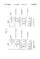
- FIG. 1is an explanatory diagram showing one example of the operation of transforming two-bits of data to be programmed in one memory cell and read therefrom into quaternary data of the level to be physically programmed in each memory cell and read therefrom in accordance with the present invention.
- FIG. 2is an explanatory diagram showing one example of the operation of inversely transforming quaternary data transformed by a data transforming logic circuit into the original two-bits of data.
- FIG. 3is an explanatory diagram showing the relations between the quaternary data and the threshold values of the memory cells.
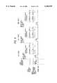
- FIG. 4is a circuit diagram schematically showing one embodiment of a multi-value flash memory according to the present invention.
- FIG. 5is a flow chart showing a programming procedure of the multi-value memory of the embodiment.
- FIG. 6is a timing diagram showing the programming operation waveforms of the multi-value flash memory of the embodiment.
- FIG. 7is an explanatory diagram of the operation waveforms showing the difference between the programming method of the multi-value flash memory of the embodiment and another programming method.
- FIG. 8is a flow chart showing a reading procedure of the multi-value flash memory of the embodiment.
- FIG. 9is a timing diagram showing the reading operation waveforms of the multi-value flash memory of the embodiment.
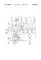
- FIG. 10is block diagram showing an example of the entire structure of the multi-value flash memory of the embodiment.
- FIG. 11is a block diagram showing an example of the system construction of an embodiment in which a controller is given a function to transform two-bits data intrinsic to the multi-value memory and quaternary data.
- FIG. 12is a diagram showing the structure of a memory cell used in the flash memory of the embodiment and the voltage state at the programming time.
- FIG. 13is a diagram showing the voltage state at the erasing time of the memory cell used in the flash memory of the embodiment.
- FIG. 14is a diagram showing the voltage state at the reading time of the memory cell used in the flash memory of the embodiment.
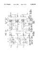
- FIG. 15is a block diagram showing an internal power source generator and a switching circuit for selecting and feeding the generated voltage to a word driver or the like.
- FIG. 16is a schematic circuit diagram showing an example of the construction of the word driver.
- FIG. 17is an explanatory diagram showing a method of an embodiment for refreshing the multi-value flash memory.
- FIG. 18is a flow chart showing a refreshing procedure of the multi-value flash memory of the embodiment.
- FIG. 19is a timing diagram showing the operation waveforms at the refreshing time.
- FIG. 20is a schematic circuit diagram showing an example of the construction of a sense latch circuit of an embodiment.
- FIG. 21is a schematic circuit diagram showing the state at the data inversion starting time and the operation of the sense latch circuit.
- FIG. 22is a schematic circuit diagram showing the state at the data inversion ending time and the operation of the sense latch circuit.
- FIG. 23is a schematic circuit diagram showing the state at the verifying time and the operation of the sense latch circuit.
- FIG. 1shows a method of transforming data to be inputted from the outside and stored, and multi-value data to be stored in memory cells
- FIG. 2shows an inverse transforming method for restoring the original data from the multi-value data.
- FIG. 1shows an example of the transformation method in which any of two bits, i.e., "00", “01", “10” and “11” is to be stored in one memory cell, although the invention is not especially limited thereto.
- the memory elements whose number is equal to that of the number of "1s" as a result of the aforementioned operationare subjected to a programming operation, i.e., the application of program pulses, they will have four types of threshold values, as shown in FIG. 1(3), according to the number of programming operations, so that two-bits of data can be programmed in one memory cell.
- the states of the changes in the threshold value distributions of the individual memory elementsare shown in FIG. 3 when the data "00", "01", “10” and "11" are to be stored in the same number in a plurality of memory elements in the memory array.
- FIG. 2shows the data reading principle.
- three kinds of data "c", "d” and "f”can be sequentially read out from one memory cell.
- one (a) of the programmed two-bits datacan be restored by executing a logic operation (d*NAND f)NAND c* on the read-out data.
- the data dare identical, as they are, to the program data b.
- symbols d* and c*designate the inverted signals of the data d and c.
- FIG. 4shows one specific example of the circuit construction for the transformation of multi-value data and the inverse transformation, as shown in FIGS. 1 and 2.
- the data of 2n-bits bit length, fed from the outside to the multi-value flash memoryare serially stored through a switch SW1 in two binary data registers REG1 and REG2 having a data width of n-bits.
- the switch SW1is changed by the output of a flip-flop FF1 driven by a clock signal CLK1 fed from the outside, although the invention is not especially limited thereto, and a clock signal CLK1', produced in a frequency divider DVD by dividing the clock signal CLK1 and having a frequency twice as large as the clock signal CLK1, is fed through a change-over circuit CHG.
- the binary registers REG1 and REG2are shifted, so that the input data are alternately latched bit by bit in the binary data registers REG1 and REG2.
- the data "a”, latched in the first binary register REG1, and the data "b”, latched in the second binary register REG2,are shifted in synchronism with the clock signal CLK2 which is fed from an internal clock generator 30 through the change-over circuit CHG, fed bit by bit to a data transforming logic circuit 11 for the operations of FIG. 1(2), and then sequentially transferred after a predetermined logic operation through a switch SW2 to a sense latch circuit 13 having an n-bits length and disposed on one side of a memory array 12, so that they are programmed in the memory cells of the memory array 12.
- the aforementioned change-over circuit CHGis switched, by a control signal coming from a sequencer 18 for controlling the memory inside, to feed the clock signal CLK1' to the binary registers REG1 and REG2 at the data input time and the clock signal CLK2 from the clock generator 30 to the binary registers REG1 and REG2 at the time of data transfer with the sense latch 13.
- the aforementioned data transforming logic circuit (the data programming operation circuit) 11is constructed to include: a NAND gate G1 which is allowed to receive at the individual input terminal the data a and b in the binary data registers REG1 and REG2 and to perform the operation (aNANDb) and a NOR gate which is also allowed to receive at the input terminal the data a, b and to perform the operation (aNORb); and an inverter G3 which is allowed to receive at its input terminal the data b of the binary data register REG2 and to perform the operation (NOTb).
- the switch SW2selects and feeds any of the output signals of those logic gates G1, G2 and G3 to the sense latch circuit 13.
- the read data "c"having appeared on a bit line in response to the setting of one word line in the memory array 12 to the read voltage level, are amplified and latched by the sense latch circuit 13 and are serially transferred through a switch SW3 to the binary data register REG1 in synchronism with the internal clock signal CLK2.
- the data "d”, read out to the sense latch circuit 13 by changing the read voltage levelare serially transferred to the binary data register REG2 through the switch SW3.
- the data "f”, read out to the sense latch circuit 13 by changing the read voltage levelare serially transferred to an inverse transforming logic circuit 14 through the switch SW3.
- the binary registers REG1 and REG2are shifted in synchronism with the clock signal CLK2.
- the period of the clock signal CLK2 at the data reading timemay be shorter than that of the clock signal CLK2 at the data programming time.
- the clock signal CLK2can be generated which has a period determined by the clock generator 30 in accordance with the control signal from the sequencer 18. The change in the word line reading level is also changed according to the control signal from the sequencer 18.
- the inverse transforming logic circuit (the data reading operation circuit) 14is constructed to include: an inverter G11 for receiving the data outputted from the binary data register REG2; a NAND gate G12 for directly receiving at its input terminals both the output of the inverter G11 and the data transferred from the sense latch circuit 13; a delay circuit DLY for delaying the data outputted from the binary data register REG1 and transmitting the delayed data at a predetermined timing; an inverter G13 for inverting the signal coming from the delay circuit DLY; and a NAND gate G14 for receiving the output of the inverter G13 and the output of the NAND gate G12.
- the shift operation of the binary registers REG1 and REG2are synchronized with the clock signal CLK2.
- the next bits of the data "c” and “d”are read out again from the binary data registers REG1 and REG2, and the logic operations (d*NAND f)NAND c* are executed for the next one bit of the read-out data "f" which are directly transferred from the sense latch circuit 13.
- the data "a”, inversely transformed by the inverse transforming logic circuit 14,do not necessarily need to be instantly outputted to the input/output terminal I/O, as described above.
- the data "a” inversely transformedmay be first latched in the binary data register REG1 and then outputted to the input/output terminal I/O alternately with the data in the binary data register REG2 after all bits have been inversely transformed.
- a one-bit latch circuitmay desirably be provided in place of the aforementioned delay circuit DLY.
- the data "c" in the binary register REG1can be read out bit by bit and logically operated with the data "d” and "f”, and the results can be simply programmed in the original bit positions in the binary data register REG1.
- the shift operations of the binary registers REG1 and REG2, when the inversely transformed data are outputted to the outside after they are once latched in the binary registers REG1 and REG2,can be synchronized with the clock signal CLK1 coming from the outside.
- the flash memory of this embodimentis equipped, although the invention is not especially so limited, with: a command register 16 for latching the command fed by an external CPU or the like; a command decoder 17 for decoding the command latched in the command register 16; and a sequencer 18 for sequentially producing and outputting the control signals for the individual circuits, such as the aforementioned switches SW2 and SW3, to execute the processings corresponding to those commands on the basis of the decoded results of the command decoder 17.
- the flash memorythus constructed decodes the commands, when fed, and executes the corresponding processing automatically.
- the aforementioned sequencer 18is constructed to include a ROM (Read Only Memory) latching a series of micro instruction groups necessary for executing the commands (or instructions), like the control unit of a CPU of the micro program type, so that the micro programs are started when the command decoder 17 generates the leading address of the micro instruction groups, which correspond to the commands, and feeds the address to the sequencer 18.
- ROMRead Only Memory
- all the memory cellsare batch-erased. As a result, all the memory cells are caused to have the highest threshold value (of about 5 V) and to be brought into the state (as shown in FIG. 3(1)) such that they store "11" as the program data.
- the batch erase operationis carried out, as shown in FIG. 13, by raising the voltage of the word line to apply a voltage of 10 V to the control gate CG of the memory cell, a voltage of 0 V to the drain through the bit line and a voltage of -5 V to the substrate (the semiconductor region p-well) thereby to inject electrons into a floating gate FG.
- the batch erase processis executed by programming in the command register 16 the erase command coming from the external CPU to instruct the erase operation.
- reference symbol psubdesignates a p-type semiconductor substrate
- pwelldesignates a p-type semiconductor well region for the base of the memory cell
- nisodesignates an n-type semiconductor isolation region for effecting the isolation from the substrate pseb at the data erasing time (at the negative voltage applying time)
- n+ in the surface of the p-type well region pwelldesignates the source and drain regions of the memory cell
- p+ in the surface of the p-type well region pwell, n+ in the surface of the isolation region niso, and p+ in the surface of the substrate psubdesignate the contact regions for reducing the resistances of the contacts with the electrodes for applying the potentials to the individual semiconductor regions.
- memory cellswhich are connected to word lines, say, one hundred and twenty eight word lines, although the invention is not especially limited thereto, so that all of the memory cells formed over one well can be batch-erased. Moreover, the memory cells can be erased in a unit of a word line by rendering the word line potential selected (10 V)/unselected (0 V) for the memory cells over one p-type well region.
- the flash memoryis brought into the program mode by programming in the command register 16 of FIG. 4 the program command coming from the external CPU.
- the program dataare inputted at a predetermined timing.
- the flash memorysends the program data to the binary data registers REG1 and REG2, so that the program data are transferred in units of two bits to the transforming logic circuit 11 and are transformed into quaternary data (at Step S1).
- the transformationsare carried out in the order of aNANDb, NOTb (inversion of b) and aNORb.
- the transformed data(the first transformation is aNANDb) are transferred to the sense latch circuit 13 (Step S2).
- Step S3it is judged whether or not all the data in the binary data registers REG1 and REG2 have been transferred. If this judgment is YES, a program pulse having a predetermined pulse width is applied to the memory cell of the bit which corresponds to the value "1" of the X (row) address fed from the external CPU and the Y (column) address outputted from a built-in Y-address counter 33, as shown in FIG. 10, (at Step S4), so that the programming is executed.
- the programmingis carried out, as shown in FIG. 12, by applying a voltage of -10 V to the control gate CG through the word line, a voltage of 5 V from the sense circuit to the drain through the bit line, and a voltage of 0 V to the substrate.
- a voltage Vcce.g., 3.3 V
- the verify voltage (about 3.5 V for the first time) corresponding to the program levelis fed to the word line, which is left in the selected state at the programming time, to read out the data in the memory cell to which the program pulse has been applied.
- the data "0"is read out as read-out data from the memory cell which has been sufficiently programmed, whereas the data "1” is read out from the memory cell which has been insufficiently programmed. It is, therefore, judged according to the programmed data whether the program has been ended or insufficient.
- the data of the sense latch circuit 13, which have been programmedare inverted to "0" (Step S6). Moreover, it is judged whether or not all the latch data of the sense latch circuit 13 take the value "0".
- Step S7the routine is returned from Step S7 to Step S4, so that the program pulse is applied again to the memory cell which is insufficiently programmed to have the value "1".
- Step S4the program pulse is repeatedly applied so that the threshold values of all the memory cells may become lower than the program verify voltage.
- the programmed memory cellshave a threshold value of about 3.2 V on an average.
- Step S8it is judged whether or not the programming operations for all the program levels have ended, that is, whether or not the data "10", "01" and "00" have been programmed. If the judgment is NO, the routine is returned to Step S1, at which quaternary data based on the next operation result (NOTb) are programmed in the memory cells to change the verify voltage of the word line (2.5 V for the second time). As a result of this verification, the programmed memory cells have a threshold value of about 2.2 V on an average. After this, the programming and verification (at a verify voltage of 1.5 V) of the third operation result are executed, so that the programmed memory cells have a threshold value of about 1.2 V on an average, thus ending the programming.
- NOTbnext operation result
- FIG. 6shows the waveforms of the control clock signal CLK2, the data to be programmed in the sense latch circuit 13, and the potential of the selected word line in the aforementioned programming and program verifying operations.
- the first operation result(aNANDb) is transferred to the sense latch circuit 13, and the selected memory cell having the latch value "1" is then programmed by the program pulse.
- a voltage of about 3.5 Vfor example, is fed as the program verify voltage to the word line, and it is judged whether or not the programmed data have the value "0".
- the threshold valueis higher than 3.5 V, the read-out data have the value "1" and are found to have been insufficiently programmed, so that the programming operations are repeated till the read-out data have the value "0".
- the second operation result (NOTb)is transferred to the sense latch circuit 13, so that the programming operation of the desired memory cell is started by the program pulse.
- the program verify voltageis set to about 2.5 V, and it is judged whether or not the programming is insufficient. If the judgment is YES, the programming is executed again.
- the third program result (aNORb)is transferred to the sense latch circuit 13, and a procedure like the aforementioned one is executed.
- the program verify voltage in this caseis about 1.5 V.
- the setting of the word line voltage at the three program verify stagesis so controlled that the voltage value is sequentially changed (3.5 V ⁇ 2.5 V ⁇ 1.5 V) away from the erase level from the starting point of the level (3.5 V) which has been set at the closest value to the erase level (about 5 V).
- the memory cell of which the target threshold value is an intermediate or lowest value2.2 V, 1.2 V
- the programming of the memory cell where target threshold value is the highest value3.2 V
- a conceivable method for setting the programming and program verifying word line voltageis one in which the setting is changed so as to execute the first programming of memory cells, as the programming object, having an intermediate threshold voltage (2.2 V) out of the three kinds of threshold voltage, and the second programming of memory cells, as the programming object, having a voltage (3.2 V) higher than the voltage of the first programming or a voltage (1.2 V) lower than that.
- FIG. 7(A)alternatively, there can be conceived a method for batch-programming the memory cells having an identical target threshold value. According to these methods, however, it takes a long time for programming, and the time for the charge/discharge to change the word line voltage is increased, so that the time for the program/verify becomes longer than that of the present embodiment.
- the data reading operationis performed, as shown in FIG. 14, by raising the voltage of the word line to apply a voltage of the selected level, such as 3.7 V, 2.7 V or 1.7 V, to the control gate CG of the memory cell, or a voltage of 1.5 V to the drain through the bit line.
- the reading operationis executed by programming the command for ordering a reading operation in the command register 16.
- the read levelis set at first to the highest level of 3.7 V to energize the word line (at Step S11). Then, in the selected memory cell, data will appear on the bit line in accordance with the word line reading voltage level, so that the data are read out by amplifying the bit line level by the sense latch circuit 13 (Step S12). Next, the subsequent steps are different depending upon whether the reading is the first, second or third reading (Step S13). Specifically, when the reading is the first reading, the read data in the sense latch circuit 13 are transferred to the binary data register REG1 (Step S14).
- Step S15When the transfer of all the read data in the sense latch circuit 13 has ended, the routine returns from Step S15 to Step S11, at which the second data reading operation is executed by setting the read level to 2.7 V to transfer the read data to the binary data register REG2.
- the third data reading operationis performed by setting the read level to 1.7 V, and the routine moves from Step S13 to Step S16, at which the read data are transferred directly to the inverse transforming logic circuit 14.
- the data, latched in the binary data registers REG1 and REG2are individually transferred bit by bit to the inverse transforming logic circuit 14, in which there is executed a logic operation for transforming the quaternary data into two bit data (Step S17).
- the foregoing procedure(Steps 16 to 18) is repeated to end the reading operations till the transfer and transformation of all the data in the sense latch circuit 13 are ended.
- the data transformationis effected by executing the operation of FIG. 2.
- FIG. 9shows the timings of the control clock CLK2 in the reading operation according to the aforementioned procedure, the data to be transferred from the sense latch circuit 13, and the read level of the word line.
- the reading operationis started to set the first read level (3.7 V) at first thereby to activate the word line, so that the data will appear on the bit line.
- the data "c”, having appeared in response to the first word line level 3.7 V,are read out by the sense latch circuit 13 and are transferred to the first binary data register REG1 having a data width equal to n bits, which represents the data length of..the sense latch.
- the data "d”, produced by lowering the word line level by a predetermined value to the second read level 2.7 V,are transferred to the second binary data register REG2.
- the data “f”, produced by lowering the word line to the third read level 1.7 V,are transferred to the inverse transforming logic circuit 14 so that the aforementioned quaternary data "c", "d” and “f” are changed again to two-bit data and outputted to the outside, such as to the CPU.
- FIG. 10shows the relation between an example of the entire construction of the multi-value flash memory MDFM having on the common semiconductor chip the aforementioned data transforming/inverse-transforming circuit, and a controller CONT connected with the flash memory MDFM.
- This controller CONTmay have only an address generating function and a command generating function for the multi-value flash memory of the present embodiment, so that a general purpose microcomputer can be used.
- the circuit components designated by the same reference symbols of FIG. 4have identical functions.
- REG1 and REG2designate binary data registers for holding the program data of two bits
- the numeral 11designates a data transforming logic circuit for transforming the held two-bits data into quaternary data
- the numeral 12designates a memory array provided with nonvolatile memory elements having a floating gate, such as a FAMOS in a matrix form
- the numeral 13designates a sense latch circuit for latching the read data and the program data
- the numeral 14designates an inverse transforming logic circuit for transforming the quaternary data read out from the memory array into two-bits data
- the numeral 16designates a command register for latching the command fed from the controller CONT
- the numeral 17designates a command decoder for decoding the command code held in the command register 16
- the numeral 18designates a sequencer for sequentially generating and outputting the control signals for the individual circuits in the memories to execute the processings
- the multi-value flash memory of this embodimentis equipped with two memory arrays, although the invention is not especially limited thereto, and individual sense latch circuits 13 are provided for the respective memory arrays. These individual sense latch circuits 13 are constructed to simultaneously amplify and latch the data of the memory cells of one line sharing the word line in the memory array, so that the read data latched in two sense latch circuits 13 are selected by a common Y-decoder 15 and transferred bit by bit or in units of a byte to an output register 19. The read data latched in the output register 19 are outputted to the external CPU or the like through a buffer circuit 22.
- the sense latch circuit 13 of the embodiment of FIG. 4performs a shift operation during the data transfer and is required to have a function similar to that of the shift register. However, the sense latch circuits 13 can have no shift function by providing a construction, as in FIG. 10, in which the data are selected by the Y-decoder 15 and in which this Y-decoder 15 shifts the selected bit in response to the clock signal.
- the multi-value flash memory of this embodimentis constructed to include, in addition to the above-specified individual circuit, an all decision circuit 20 for deciding whether or not the data read out from the memory array 12 and fed to the sense latch 13 are all "0" or all "1"; a buffer circuit 21 for fetching external control signal, such as a reset signal RES, a chip select signal CE, a program control signal WE, an output control signal OE, a system clock SC and a command enable signal CDE indicating whether the input is a command input or an address input, all signals being fed from the controller CONT; a buffer circuit 22 for fetching an address signal and a command signal; an internal signal generator 23 for generating a control signal for an internal circuit on the basis of the external control signal; an address register 24 for latching the address which has been held in the buffer circuit 22; a data register 25 for latching the input data; X-address decoders 26a and 26b for decoding the fetched address to generate a signal and for selecting the word line in the memory array
- the multi-value flash memory of this embodimentis given a function (hereinafter referred to as the refresh function) to sharpen the bell-shaped variation distributions of the threshold values when the shapes broaden and lower due to the disturb or the retention influences (see FIG. 3).
- This refresh functionis activated when a command is fed from the outside as in the programming or erasing operation. If the refresh command is fetched by the command register 16, the sequencer 18 of the micro program control type is started to effect the refreshing operation. This refreshing operation will be described in detail hereinafter.
- the signal indicating the decision result of the aforementioned all decision circuit 20is fed to the sequencer 18. In the refreshing mode, the all decision circuit 20 decides that the read data are all "0".
- the sequencer 18stops the refreshing operation.
- the sequencer 18stops the erasing operation if the aforementioned all decision circuit 20 decides that the read data are all "1".
- a predecode systemin which the X-address decoder decodes the address signal at the two stages by means of the predecoder 26a and the main decoder 26b.
- the desired word lineis selected, for example, by decoding the more significant three bits of the X-address at first using the predecoder 26a and by controlling the word driver 27 with the predecode signal.
- the unit decoders constituting the main decoder 26bcan be arranged in a high integration state according to the word line pitch of the memory array thereby to reduce the chip size.
- the multi-value flash memory of the aforementioned embodimentis equipped on the common silicon substrate, as shown in FIGS. 4 and 10, with the function circuits 11 and 14 for transforming two-bits data into quaternary data and vice versa.
- a dedicated controller unit having those functionscan be separately provided.
- the flash memory chipneed not be provided with the functions intrinsic to the multi-value, so that its chip area does not increase.
- Another advantageis that a plurality of flash memories MDFM can be connected to a single controller unit CONT and controlled by a bus BUS, as shown in FIG. 11.
- This controller unitis constructed to have an address generating function and a command generating function in addition to the aforementioned data transforming/inverse-transforming functions.
- FIG. 15shows the internal power source generator 28 for generating the word line voltage and a substrate potential Vsub and the switching circuit 29 for selectively feeding them to the word driver 27 and the like
- FIG. 16shows an example of the construction of the word driver 27.
- the internal power source generator 28generates the necessary word line voltages in response to the internal control signals which are generated from the sequencer 18 in correspondence to the various operation modes.
- the construction of the internal power source generator 28 for generating voltages including the word line voltage and the construction of the switching circuit (the word line voltage switching circuit) 29 for receiving the generated voltagesare similar to those of the prior art, except that the kinds of the voltage values of the word line are increased for the multi-value operation.
- the read voltage(2.7 V, 0 V); the program voltage (-10 V, 0 V); the program verify voltage (1.5 V); the erase voltage (+10 V, 0 V) and the erase verify voltage (4.3 V, 0 V).
- the word line voltages necessary for the multi-value flash memory of the present embodimentare: the read voltage (3.7 V, 2.7 V, 1.7 V, 0 V); the program voltage (-10 V, 0 V); the program verify voltage (3.5 V, 2.5 V, 1.5 V); the erase and erase verify voltages (10 V, 4.3 V, 0 V); and the refresh voltage (-10 V, 10 V, 3.7 V, 3.5 V, 2.7 V, 2.5 V, 1.7 V, 1.5 V, 0 V).
- the aforementioned switching circuit 29receives the internal control signals, which are generated by the sequencer 18 and correspond to the various operation modes, and feeds the voltages, generated by the aforementioned internal power source generator 28, to the power terminals P1 and P2 of the word driver 27 which is constructed as shown in FIG. 16.
- a word driver WDRV of FIG. 16is a driver used when the word line predecoding method is adopted.
- Eight voltage selectors VOLS1 to VOLS8have their inputs connected in common to the output node N1 of a logic selector LOGS1
- eight voltage selectors VOLS9 to VOLS16have their inputs connected in common to the output node N2 of a logic selector LOGS2, so that the individual voltage selectors may be selected by predecode signals Xp1 and Xp1* to Xp8 and Xp8*.
- Signals XM and XN together with the predecode signals Xp1 and Xp1* to Xp8 and Xp8*are fed from an address decoder XDCR (26b).
- the voltage selectors VOLS1 to VOLS16have to select and feed the same voltage to the word line as that which is unselected by the other logic selector, unless the operation is selected by the predecode signal even if either logic selector LOGS1 or LOGS2 corresponding to the voltage selectors outputs the select signal of the select level.
- separating MOSFETs Q56 and Q57are switched by the predecode signal.
- a pull-up MOSFET Q58 and a pull-down MOSFET Q59which can be switched complementarily with the separating MOSFETs Q56 and Q57 to feed a predetermined voltage to each input of the output circuit INV2.
- the aforementioned signal XMis deemed to be a three-bit signal for indicating which word lines out of the eight word line groups each including eight word lines is to be selected.
- the predecode signals Xp1 and Xp1* to Xp8 and Xp8*are deemed to be complementary signals for indicating which word line contained in each word line group is to be selected.
- the high level of the select signal SELis the select level
- the high and low levels of each of the predecode signals Xp1 and Xp1* to Xp8 and Xp8*are the select level.
- the voltage to be fed to the terminal P1 of the aforementioned word driver WDRVis a voltage Vpp to be used for the erasing, programming, verifying and reading operations, such as 5 V, 4.3 V, 3.7 V, 3.5 V, 2.7 V, 2.5 V, 1.7 V, 1.5 V or 0 V.
- the voltage to be fed to the terminal P2is either a voltage Vee to be used for the programming and refreshing operations, such as -10 V or a voltage Vss as the ground potential or the reference potential of the circuit, such as 0 V.
- Each of the aforementioned logic selectors LOGS1 and LOGS2is constructed to include: an inverter INV1 for inverting the signal of the X-decoder XDCR; a transfer gate TG1 for transmitting or blocking the output of the inverter INV1; and a transfer gate TG2 for transferring or blocking the signal of the X-decoder XDCR.
- the aforementioned voltage selectors VOLS1 to VOLS16are made to have identical constructions, each of which is made, as represented by the voltage selector VOLS1, of: an N-channel type pull-up MOSFET Q58 connected between a terminal P3 and the gate of a MOSFET Q52 and switched by the predecode signal Xp1*; and a P-channel type pull-up MOSFET Q59 connected between a terminal P4 and the gate of a MOSFET Q53 and switched by the predecode signal Xp1.
- the voltage selector VOLS1switches the separating MOSFET Q56 by using the predecode signal Xp1 and the other separating MOSFET Q57 by using the predecode signal Xp1*.
- the aforementioned terminals P3 and P4are fed with the voltage Vcc or Vss.
- Table 1shows the voltages at the terminals and the word line voltages in the individual operation modes. The description of the manner in which to set the program mode, the erase mode and the read mode will be omitted.
- the switching circuit 29feeds the voltage Vpp to the terminal P1, the voltage Vss to the terminal P2, and the voltage Vcc to the terminals P3 and P4, and the control signal DE is set to the low level.
- all the bits of the signal XMare set to the low level, so that any of word lines W1 to W8 can be selected.
- the select signal SEL at the select levelthe high level
- the node N1is set to the low level through the inverter INV1 and the transfer gate TG1 so that this low level is fed to the inputs of the individual voltage selectors VOLS1 to VOLS8.
- the memory cell to be erasedis coupled to the word line W1, only the signals Xp1 and Xp1* of the predecode signals Xp1 and Xp1* to Xp8 and Xp8* are set to the high level and the low level, respectively.
- the separating MOSFETs Q56 and Q57 of only the voltage selector VOLS1are turned on, so that the signal at the node N1 is fetched by the voltage selector VOLS1.
- both the pull-up MOSFET Q58 and the pull-down MOSFET Q59 of the voltage selector VOLS1are cut off.
- the signal of the node N1is fed to the MOSFETs Q52 and Q53 of the voltage selector VOLS1.
- the MOSFET Q52 of the output circuit INV2is turned on, and hence the word line W1 begins to be charged by the voltage Vpp at the terminal P1.
- the low level to be fed to the gate of the other MOSFET Q53is raised to a low level higher than the initial voltage Vss by the action of the MOSFET Q57, so that the MOSFET Q53 is not completely cut off.
- the conductance of a feedback MOSFET Q55is increased with the rise of the level of the word line W1, the voltage of the gate of the MOSFET Q53 is forced to the voltage Vss, and it is completely cut off.
- the word line W1 to which is coupled the selected memory cellis charged to the level Vpp.
- the predecode signals Xp1 and Xp1*are set to the low level and the high level, respectively, if the memory cell Q1 of the word line W1 is not selected for the erasure.
- both separating MOSFETs Q56 and Q57 of the voltage selector VOLS1are turned off to fetch no signal from the node N1.
- both pull-up MOSFET Q58 and pull-down MOSFET Q59 of the voltage selector VOLS1are turned on.
- the gates of the MOSFETs Q52 and Q53 of the voltage selector VOLS1are fed with the voltage Vcc from the terminals P3 and P4 through the MOSFETs Q58 and Q59.
- the MOSFET Q53 of the output circuit INV2is turned on, so that the word line W1 begins to be discharged to the voltage Vss through the terminal P2.
- the high level fed to the gate of the other MOSFET Q52is lower than the voltage Vcc by the threshold voltage of the MOSFET Q58, so that the MOSFET Q52 is not completely cut off.
- the conductance of the feedback MOSFET Q54is increased, and the gate of the MOSFET Q52 is forced to the voltage Vpp, so that it is completely cut off. In the erase mode, therefore, the unselected word line W1 is discharged to the voltage Vss.
- the word driver WDRV when the program mode or the read mode is specifiedwill not be described in detail because it is similar to the operation of the aforementioned program mode.
- the word linesare so driven by the voltages applied to the terminals P1 and P2 from the switching circuit 29 that the voltages, as shown in FIGS. 13 and 14, may be applied to the selected memory cells.
- the refreshing operationwhich is a second feature of the multi-value flash memory of the present inventions will be described with reference to FIG. 17.
- the bell-shaped variation distributions of the threshold valuesare completely separated, as shown in FIG. 17(1).
- the threshold value variationsare increased as shown in FIG. 17(2), as the subsequent programming, reading and standby state operations are repeatedly executed.
- This phenomenonmay occur even in an ordinary flash memory for storing only one bit, but may cause a malfunction in the multi-value flash memory in which the intervals between the individual threshold values are narrow, as in the foregoing embodiment.
- FIG. 18is a flow chart showing the procedure of the refreshing operation.
- the sequencer 18is started to begin the refreshing operation according to the flow chart of FIG. 18.
- a weak erase pulseis applied at first from the word line to all the memory cells which are connected to the selected word line (Step S21).
- the threshold values of all the memory cellsare slightly shifted to the higher side, as shown in FIG. 17(3). This shift is about 0.2 V, although the invention is not especially limited thereto.
- the term, weak erase pulserefers to a sufficiently short pulse that the memory cell threshold value at "10", for example, may not exceed, if added, just the higher read level 3.7 V.
- the pulse widthis experimentally determined according to the amount to be shifted.
- the word line voltageis set to the read level (3.7 V) corresponding to the stored data "10" (Step S22) thereby to effect the reading operation.
- dataare read out according to the threshold values of the individual memory cells (Step S23) and are amplified and latched by the sense latch circuit 13.
- the data of the sense latch corresponding to the memory cell having a higher threshold value than the word line voltageis set to "1"
- the data of the sense latch corresponding to the memory cell having a lower threshold value than the word line voltageis set to "0”.
- the data of the sense latchare inverted (Step S24). This data inversion can be easily carried out (as will be described hereinafter) by the sense latch circuit having the construction shown in FIG. 20.
- the word lineis set to a lower verify voltage (3.5 V at first) which is lower than the aforementioned read level (Step S22) so that the judgment of the threshold value is executed (Step S25).
- the data of the sense latch corresponding to the memory cell (designated by letter A in FIG. 17(4)) having a lower threshold value than the verify voltageare switched from "0" to "1".
- the data of the sense latch corresponding to the memory cell (designated by letter B in FIG. 17(4)) having a higher threshold value than the verify voltageare left at "1".
- the memory cell (designated by letter B in FIG. 17(4)) having the data "1" of the sense latchis re-programmed by setting the program voltage (Step S27).
- the verificationis executed by setting the verify voltage corresponding to the program level (Step S28, S29).
- the threshold valuebecomes lower than the verify voltage
- the latch datachange from "1" to "0”.
- the programming and verifying operationsare repeated to end the refresh procedure of the memory cell having the data "10", till all the latch data change to "0".
- the variation distribution (the half-value width) of the threshold value of the memory cell of the data "10"becomes low, as indicated in FIG. 17(5).
- Step S31Similar refreshing operations are executed, too, for the memory cells for storing the data "01" and "00" (Step S31).
- Step S32the operations of Steps 21 to 31 are repeated to complete the refresh operation (Step S32) when a predetermined number of operations are ended.
- Table 2shows the changes in the latched data of the sense latch circuit which occur sequentially when the memory cells having the threshold values indicated by letters A, B and C of FIG. 17(4), are read out, when the refreshing is executed according to the procedure described above.
- FIG. 19is a diagram showing the timings at which the refreshing operations are executed.
- the causes of enlarging the variations of the threshold values of the memory cellsare the disturb influence due to the execution of the weak programming, erasing and reading operations of a memory cell adjacent to a memory cell if this memory cell is programmed or read, and the retention influence due to the natural leakage.
- the timings at which the refreshing operations against the fluctuation of the threshold values due to the disturb influence are executedare as follows.
- the refreshing operationsare executed when the flash memory is in a standby state (/RES is at the high level) and after a predetermined number of programming/erasing and reading operations are completed.
- the /RESis set to the low level immediately before the power supply is turned off, so that the refresh is executed by sensing the off condition.
- the refreshis executed after the power supply is turned on to set the /RES to the high level.
- the refreshing operations described aboveshould not be limited to the multi-value flash memory.
- the power supply voltage of the flash memorywill change to a lower voltage, however, an increase in the variation of the threshold value cannot be ignored even in an ordinary flash memory, so that the refreshing operation is an effective function as a counter-measure against the lower power supply voltage of the flash memory.
- FIG. 20shows an example of the construction of the memory array 12 and the sense latch circuit 13.
- the memory array 12is an AND type, in which a plurality of memory cells MC (e.g., one hundred and twenty eight for one hundred and twenty eight batch-erasable word lines) are connected in series between a common drain line DL, provided in parallel with the bit lines BL arranged perpendicularly to the word lines and adapted to output the read signal of the selected memory cell, and a common source line SL.
- the common drain line DLcan be connected to the corresponding bit line BL through the switch MOSFET Q1, and the common source line SL can be connected to the grounding point through the switch MOSFET Q2.
- the gate control signals for those switch MOSFETs Q1 and Q2are generated on the basis of the X-address signal and the read/write control signal.
- the switch MOSFETs Q1 and Q2are turned on to discharge the bit lines through the ON memory cells by setting the gate control signals to a potential such as Vcc (3.3 V) at the data reading time (including the verifying time).
- Vcc3.3 V
- the gate control signal for the switch MOSFET Q1is set to a potential such as 7 V and turned on because the program voltage (5 V) of the bit lines is transmitted to the drains of the memory cells.
- the switch MOSFET Q2 on the common source line SL sideis turned off.
- the sense latch circuit 13is constructed of a CMOS differential type sense amplifier SA disposed for each memory column for amplifying the potential difference between the bit lines of the right and left memory arrays.
- the bit line of the selected side (on the lefthand side) memory arrayis precharged to a potential such as 1 V by a precharge MOS (SW21), and the bit line on the opposite side memory array is precharged to a potential such as 0.5 V by a precharge MOS (SW22).
- the bit lineWhen the word line WL is set to the read level in this precharge state, the bit line retains 1.0 V if the selected memory cell has a high threshold value. However, if the selected memory cell has a low threshold value, an electric current flows to draw the charge on the bit line, so that the bit line takes a potential of 0.2 V. The potential difference between this potential of 1.0 V or 0.2 V and the potential of 0.5 V of the bit line on the opposite side is detected and amplified by the sense amplifier SA, so that the read data are latched in the sense amplifier SA.
- the sense latch (the sense amplifier) corresponding to the bit line connected to the memory cell to be programmedis set to "1"
- the program pulse (-10 V)is applied to the word line
- the word lineis set to the verify voltage (about 3.5 V for the first time) corresponding to the program level thereby reading the memory cell to which the program pulse is applied.
- the read data "1"are read out from the insufficiently programmed memory cell to the bit line, and a program end or weak program is judged from the data read out, so that the data of the sense latch (the sense amplifier) whose bits are programmed are inverted to "0".
- the data "1"are left in the sense latch (the sense amplifier) corresponding to the insufficiently programmed memory cell, so that the program pulse may be applied again to the insufficiently programmed memory cell corresponding to the bit of "1".
- the data read out to the sense latchare inverted, and the verification is executed to apply the program pulse to the memory cell corresponding to the bit of "1".
- the sense latch circuit of FIG. 20is devised to have a inversion control circuit 30 which is interposed between the sense amplifier and the memory array and composed of four switches SW11, SW12, SW13 and SW14, so as to easily facilitate the inversion of the latch data of the sense amplifier corresponding to the memory cell, which has been programmed at the aforementioned programming time, and the narrowing of the memory cell to which the program pulse is to be applied.
- the switches SW21 and SW22 disposed on the individual bit lines BLare switches for precharging the bit lines and are constructed of MOSFETs, similar to the aforementioned switches SW11 to SW14.
- the switch SW13is turned off at first. With the bit line BL and the sense amplifier SA disconnected from each other, as shown in FIG. 20, the switches SW21 and SW22 are then turned on to charge the bit line BL on the selected side to a precharge level of 1.0 V.
- the bit line on the unselected sideis charged to the level of 0.5 V.
- the sense amplifier SAturns on the switch SW14 to reset it and feed it a potential of 0.5 V.
- the switch MOSFETs Q1 and Q2are turned on by impressing the voltage Vcc to their gates.
- any word line WL in the memory arrayis set to the select level of 3.7 V.
- the memory cellse.g., the cell A and B of FIG. 17
- the memory cellshaving a lower threshold value than the word line select level are turned on, so that the bit line BL connected to them is discharged to the level of 0.2 V by the electric current flowing to the common source line SL through the ON memory cells.
- the memory celle.g., the cell C of FIG. 17
- the memory cell having a higher threshold value than the word line select levelis turned off, so that the bit line BL connected to it is held at the precharge level of 1.0 V.
- the switch SW14is turned off to release the sense amplifier SA from the reset state and to activate it, and the switch SW13 on the bit line BL is turned on to connect the bit line BL to the sense amplifier SA.
- the power source voltage Vccis fed to the P-MOS side of the sense amplifier SA, and the ground potential (0 V) is fed to the N-MOS side.
- the sense amplifier SAamplifies the potential difference between the bit lines BL and BL* sufficiently, and the switch SW13 on the bit line BL is turned off. As a result, the sense amplifier SA comes into the state that it amplifies the level difference between the bit lines on the select and unselect sides and holds the data.
- the switch SW12is turned off, so that the bit line BL retains the level Vcc. In short, the inverse level of the latched data of the sense amplifier SA appears in the corresponding bit line BL.
- the switch SW14is first turned on to reset the sense amplifier SA. After this, the switch SW14 is turned off, and the switch SW13 to the bit line BL is turned on to connect the bit line BL to the sense amplifier SA. In the meantime, the supply voltages on the P-MOS side and the N-MOS side of the sense amplifier SA are set to 0.5 V. Then, the supply voltage Vcc is fed to the P-MOS side of the sense amplifier SA whereas the ground potential (0 V) is fed to the N-MOS side, and the switch SW13 on the bit line BL is turned off. As a result, the sense amplifier SA takes the state that it latches the data corresponding to the level of the bit line in the aforementioned data latching state, as shown in FIG. 22.
- the sense amplifiers corresponding to the cells A and B of FIG. 17latch the high level "1", and the sense amplifier corresponding to the cell C latches the low level "0".
- These operationsare similar to the so-called "program verifying” operation.
- the bit line prechargehas to be executed only for the portion in which the sense latch is "H”.
- the switch SW11By turning on the switch SW11 to set the bit line precharge voltage (1) to 1 V, therefore, only bit lines BL0 and BL1 take the value of 1 V (the bit line BL2 is reset in advance to 0 V).
- the switches SW21 and SW22are turned on while the switch SW13 on the bit line BL is left off, to charge the select side bit line BL to the precharge level of 1.0 V and the unselected-side bit line to the level of 0.5 V.
- a verify voltagesuch as 3.5 V slightly lower than the preceding read level (3.7 V) is applied to the selected word line.
- the memory celle.g., the cell A of FIG. 17 having a lower threshold value than the word line selection level is turned on, so that the bit line BL connected thereto is discharged to the level such as 0.2 V.
- the memory celle.g., the cell B of FIG. 17
- the bit line BL connected theretoretains the precharge level of 1 V.
- the bit linewhich is connected to the memory cell (e.g., the cell C of FIG. 17) corresponding the data "11" having the highest threshold value, intrinsically retains the low level, i.e., "0", it takes the low level even if it is off when the word line is set to the select level (FIG. 23).
- the switch SW13 on the bit line BLis turned on. Then, the sense amplifier corresponding to the bit line, which is connected to the memory cell (e.g., the cell C of FIG. 17) corresponding to the data "11", and the sense amplifier corresponding to the bit line, which is connected to the memory cell (e.g., the cell A of FIG. 17) having a lower threshold valve than the word line select level, retain the low level "0", whereas the sense amplifier corresponding to the bit line, which is connected to the memory cell (e.g., the cell B of FIG. 17) having a higher threshold value than the word line select level, retains the high level "1".
- this data retained by the sense amplifierare used to make a shift to the programming operation to apply the program pulse (-10 V) to the selected word line, thereby lowering the threshold value of the memory cell corresponding to the retained data "1" of the sense amplifier.
- the reading operationis executed by setting the word line again to the selection level. Then, the bit line of the memory cell having a lower threshold value than the word line verify level is changed to the low level, i.e., "0", and the bit line connected to the insufficiently programmed memory cell retains the high level "1".
- the sense amplifierBy latching this state by the sense amplifier to execute the programming operation again, only the threshold value of the memory cell, in which the latched data of the sense latch corresponds to "1", is lowered to sharpen the threshold value distribution shape.
- the data latched by the sense amplifier Aare fed to the aforementioned all decision circuit 20 through both so-called column switch turned on/off by the output signal of the Y-decoder 15 and the common I/O line, and it is judged whether or not they are all "0". If they are all "0", the refresh for the memory cells of the data "10” are ended, and the refresh for the memory cells of the data "01" and "00" is executed.
- the re-programming operation of the insufficiently programmed memory cell in the aforementioned program modeis identical to the aforementioned one effected by the sense latch circuit 13 at the refreshing time.
- data of a plurality of bitsare transformed by a data transforming logic circuit into data (multi-value data) according to the combination of the bits, and the transformed data are sequentially transferred to a latch circuit connected to the bit lines of a memory array.
- a program pulseis generated according to the data latched in the latch circuit and is applied to a memory element in a selected state, so that a threshold value is made to correspond to the multi-value data.
- the states of the memory elementsare read out by changing the read voltage to intermediate values of the individual threshold values and are transferred to and latched in a register for storing the multi-value data, so that the original data may be restored by a data inverse transforming logic circuit on the basis of the multi-value data stored in the register.
- the peripheral circuit scale of the memory arraycan be suppressed to a relatively small size.
- the verify voltage value of the word lineis sequentially changed by a predetermined value in a direction away from the near side of the erasing word line voltage so that the total number of the program pulses, i.e., the program time period can be reduced compared to the multi-value flash memory system, in which the verify voltage is set at random, thereby to realize a programming operation performed in a short time.
- the memory elementwhich has a threshold value lower than the read level of the word line and higher than the verify level, is detected, and the program is executed so that the threshold value of the memory element may be lower than the verify voltage, thereby narrowing the width of the variation distribution shape of the threshold voltage of the memory element which is programmed according to the individual input data.
- the variation distribution shape of the threshold voltage of the memory elementswhich has been widened due to the disturb or the retention influences, can be returned to the steep shape substantially identical to that just after the end of the programming operation.
- the quaternary dataare stored by setting the threshold value of one memory cell at four stages, but these threshold values can be set to three stages or five or more stages.
- the inversion of the read data at the refreshing time and the narrowing of the memory cells, in which the read data are to be programmedcan be effected by using only the sense latch circuit.
- a register for latching the read data and a logic circuit for narrowing the memory cell to be programmedby performing a logic operation, e.g., by inverting the content of the register.
- the three kinds of operationsare executed as a transformation of the two-bits data into the quaternary data and vice versa.
- the logic operationshould not be limited to those of FIG. 1 but may be any logic operation as long as data having different numbers of bits of "1" can be resultantly obtained.
- the operation for data inverse transformationshould not be limited to those of FIG. 2 but may be any operation as long as the original two-bits data can be restored, and the number of operations should not be limited to one but may be two or more.
- the programming method for each memory cellshould not be limited to that of the embodiment in which the threshold value is lowered by the program pulse after it has been first raised for the erasure, but may be the one in which the threshold value is raised by the program pulse.
- the threshold valueis changed by programming the memory cell corresponding to the sense latch latching the data "1".
- the threshold valuemay be changed by programming the memory cell which corresponds to the sense latch latching the data "0".
- the description thus far madeis directed mainly to a batch-erase type flash memory to which our invention is applied and which is the field of application of its background.
- the present inventionshould not be limited thereto but can be applied generally to a nonvolatile memory device having FAMOSs as its memory elements and further widely to a semiconductor memory device which is equipped with memory cells having a plurality of threshold values.
- the present inventionit is possible to realize a multi-value type nonvolatile memory device which can carry out programming, reading and erasing operations of high accuracy which are performed in a short time period while minimizing the increase in the circuit scale, and a nonvolatile memory device capable of sharpening the shape of the variation distribution of the threshold values of memory elements while stably operating at a low voltage.
Landscapes
- Engineering & Computer Science (AREA)
- Computer Hardware Design (AREA)
- Read Only Memory (AREA)
- Dram (AREA)
Abstract
Description
TABLE 1 __________________________________________________________________________ P4 P1 P3 P2 WORD SELECTED UNSELECTED XM Xp DE ⊚ ∘ ⊙ LINE __________________________________________________________________________ERASE ∘ L H L Vcc Vpp Vcc Vss Vpp ∘ H H Vss ∘ L/H L Vss PROGRAM ∘ L H H Vss Vcc Vss Vee Vee ∘ H H Vcc ∘ L/H L Vcc READ ∘ L H L Vcc Vcc Vcc Vss Vcc ∘ H H Vss ∘ L/H L Vss __________________________________________________________________________
TABLE 2 ______________________________________ READ INVERSION VERIFY END ______________________________________CELL A 0 1 0 0CELL B 0 1 1 0CELL C 1 0 0 0 ______________________________________
Claims (19)
Priority Applications (1)
| Application Number | Priority Date | Filing Date | Title |
|---|---|---|---|
| US09/106,344US6166949A (en) | 1995-01-31 | 1998-06-29 | Nonvolatile memory device and refreshing method |
Applications Claiming Priority (4)
| Application Number | Priority Date | Filing Date | Title |
|---|---|---|---|
| JP7-14031 | 1995-01-31 | ||
| JP1403195 | 1995-01-31 | ||
| US08/860,793US5889698A (en) | 1995-01-31 | 1995-11-07 | Nonvolatile memory device and refreshing method |
| US09/106,344US6166949A (en) | 1995-01-31 | 1998-06-29 | Nonvolatile memory device and refreshing method |
Related Parent Applications (1)
| Application Number | Title | Priority Date | Filing Date |
|---|---|---|---|
| US08/860,793ContinuationUS5889698A (en) | 1995-01-31 | 1995-11-07 | Nonvolatile memory device and refreshing method |
Publications (1)
| Publication Number | Publication Date |
|---|---|
| US6166949Atrue US6166949A (en) | 2000-12-26 |
Family
ID=11849793
Family Applications (32)
| Application Number | Title | Priority Date | Filing Date |
|---|---|---|---|
| US08/860,793Expired - LifetimeUS5889698A (en) | 1995-01-31 | 1995-11-07 | Nonvolatile memory device and refreshing method |
| US09/053,494Expired - LifetimeUS6038165A (en) | 1995-01-31 | 1998-04-02 | Nonvolatile memory device and refreshing method |
| US09/106,344Expired - LifetimeUS6166949A (en) | 1995-01-31 | 1998-06-29 | Nonvolatile memory device and refreshing method |
| US09/131,395Expired - LifetimeUS6038167A (en) | 1995-01-31 | 1998-08-07 | Nonvolatile memory device and refreshing method |
| US09/287,187Expired - LifetimeUS6111790A (en) | 1995-01-31 | 1999-04-06 | Non-volatile memory device and refreshing method |
| US09/472,178Expired - LifetimeUS6226198B1 (en) | 1995-01-31 | 1999-12-27 | Nonvolatile memory device and refreshing method |
| US09/583,949Expired - LifetimeUS6256230B1 (en) | 1995-01-31 | 2000-05-31 | Nonvolatile memory device and refreshing method |
| US09/817,021Expired - LifetimeUS6366495B2 (en) | 1995-01-31 | 2001-03-27 | Nonvolatile memory device and refreshing method |
| US10/020,873Expired - LifetimeUS6459614B1 (en) | 1995-01-31 | 2001-12-19 | Non-volatile memory device and refreshing method |
| US10/223,370Expired - Fee RelatedUS6804147B2 (en) | 1995-01-31 | 2002-08-20 | Clock synchronized non-volatile memory device |
| US10/223,220Expired - Fee RelatedUS6801452B2 (en) | 1995-01-31 | 2002-08-20 | Clock synchronized non-volatile memory device |
| US10/223,485Expired - LifetimeUS6757194B2 (en) | 1995-01-31 | 2002-08-20 | Clock synchronized non-volatile memory device |
| US10/223,361Expired - Fee RelatedUS6847549B2 (en) | 1995-01-31 | 2002-08-20 | Clock synchronized non-volatile memory device |
| US10/223,347Expired - Fee RelatedUS6768672B2 (en) | 1995-01-31 | 2002-08-20 | Clock Synchronized Non-Volatile Memory Device |
| US10/373,712Expired - Fee RelatedUS6751120B2 (en) | 1995-01-31 | 2003-02-27 | Clock synchronized non-volatile memory device |
| US10/373,709Expired - LifetimeUS6751119B2 (en) | 1995-01-31 | 2003-02-27 | Clock synchronized non-volatile memory device |
| US10/373,707Expired - Fee RelatedUS6898118B2 (en) | 1995-01-31 | 2003-02-27 | Clock synchronized non-volatile memory device |
| US10/373,751Expired - LifetimeUS6747941B2 (en) | 1995-01-31 | 2003-02-27 | Clock synchronized non-volatile memory device |
| US10/373,737Expired - Fee RelatedUS6868006B2 (en) | 1995-01-31 | 2003-02-27 | Clock synchronized non-volatile memory device |
| US10/797,012Expired - Fee RelatedUS6829163B2 (en) | 1995-01-31 | 2004-03-11 | Clock synchronized nonvolatile memory device |
| US10/810,613Expired - Fee RelatedUS7193894B2 (en) | 1995-01-31 | 2004-03-29 | Clock synchronized nonvolatile memory device |
| US10/810,624Expired - Fee RelatedUS6965525B2 (en) | 1995-01-31 | 2004-03-29 | Clock synchronized nonvolatile memory device |
| US10/810,626Expired - Fee RelatedUS6850434B2 (en) | 1995-01-31 | 2004-03-29 | Clock synchronized nonvolatile memory device |
| US10/810,631Expired - Fee RelatedUS6912156B2 (en) | 1995-01-31 | 2004-03-29 | Clock synchronized nonvolatile memory device |
| US11/024,643Expired - Fee RelatedUS7161830B2 (en) | 1995-01-31 | 2004-12-30 | Clock synchronized nonvolatile memory device |
| US11/088,945Expired - Fee RelatedUS7286397B2 (en) | 1995-01-31 | 2005-03-25 | Clock synchronized nonvolatile memory device |
| US11/429,318Expired - Fee RelatedUS7324375B2 (en) | 1995-01-31 | 2006-05-08 | Multi-bits storage memory |
| US11/600,798Expired - Fee RelatedUS7327604B2 (en) | 1995-01-31 | 2006-11-17 | Clock synchronized non-volatile memory device |
| US11/892,041Expired - Fee RelatedUS7542339B2 (en) | 1995-01-31 | 2007-08-20 | Clock synchronized non-volatile memory device |
| US12/434,794AbandonedUS20100020615A1 (en) | 1995-01-31 | 2009-05-04 | Clock synchronized non-volatile memory device |
| US13/453,079Expired - Fee RelatedUS8804431B2 (en) | 1995-01-31 | 2012-04-23 | Clock synchronized non-volatile memory device |
| US14/305,270AbandonedUS20150155049A1 (en) | 1995-01-31 | 2014-06-16 | Clock synchronized non-volatile memory device |
Family Applications Before (2)
| Application Number | Title | Priority Date | Filing Date |
|---|---|---|---|
| US08/860,793Expired - LifetimeUS5889698A (en) | 1995-01-31 | 1995-11-07 | Nonvolatile memory device and refreshing method |
| US09/053,494Expired - LifetimeUS6038165A (en) | 1995-01-31 | 1998-04-02 | Nonvolatile memory device and refreshing method |
Family Applications After (29)
| Application Number | Title | Priority Date | Filing Date |
|---|---|---|---|
| US09/131,395Expired - LifetimeUS6038167A (en) | 1995-01-31 | 1998-08-07 | Nonvolatile memory device and refreshing method |
| US09/287,187Expired - LifetimeUS6111790A (en) | 1995-01-31 | 1999-04-06 | Non-volatile memory device and refreshing method |
| US09/472,178Expired - LifetimeUS6226198B1 (en) | 1995-01-31 | 1999-12-27 | Nonvolatile memory device and refreshing method |
| US09/583,949Expired - LifetimeUS6256230B1 (en) | 1995-01-31 | 2000-05-31 | Nonvolatile memory device and refreshing method |
| US09/817,021Expired - LifetimeUS6366495B2 (en) | 1995-01-31 | 2001-03-27 | Nonvolatile memory device and refreshing method |
| US10/020,873Expired - LifetimeUS6459614B1 (en) | 1995-01-31 | 2001-12-19 | Non-volatile memory device and refreshing method |
| US10/223,370Expired - Fee RelatedUS6804147B2 (en) | 1995-01-31 | 2002-08-20 | Clock synchronized non-volatile memory device |
| US10/223,220Expired - Fee RelatedUS6801452B2 (en) | 1995-01-31 | 2002-08-20 | Clock synchronized non-volatile memory device |
| US10/223,485Expired - LifetimeUS6757194B2 (en) | 1995-01-31 | 2002-08-20 | Clock synchronized non-volatile memory device |
| US10/223,361Expired - Fee RelatedUS6847549B2 (en) | 1995-01-31 | 2002-08-20 | Clock synchronized non-volatile memory device |
| US10/223,347Expired - Fee RelatedUS6768672B2 (en) | 1995-01-31 | 2002-08-20 | Clock Synchronized Non-Volatile Memory Device |
| US10/373,712Expired - Fee RelatedUS6751120B2 (en) | 1995-01-31 | 2003-02-27 | Clock synchronized non-volatile memory device |
| US10/373,709Expired - LifetimeUS6751119B2 (en) | 1995-01-31 | 2003-02-27 | Clock synchronized non-volatile memory device |
| US10/373,707Expired - Fee RelatedUS6898118B2 (en) | 1995-01-31 | 2003-02-27 | Clock synchronized non-volatile memory device |
| US10/373,751Expired - LifetimeUS6747941B2 (en) | 1995-01-31 | 2003-02-27 | Clock synchronized non-volatile memory device |
| US10/373,737Expired - Fee RelatedUS6868006B2 (en) | 1995-01-31 | 2003-02-27 | Clock synchronized non-volatile memory device |
| US10/797,012Expired - Fee RelatedUS6829163B2 (en) | 1995-01-31 | 2004-03-11 | Clock synchronized nonvolatile memory device |
| US10/810,613Expired - Fee RelatedUS7193894B2 (en) | 1995-01-31 | 2004-03-29 | Clock synchronized nonvolatile memory device |
| US10/810,624Expired - Fee RelatedUS6965525B2 (en) | 1995-01-31 | 2004-03-29 | Clock synchronized nonvolatile memory device |
| US10/810,626Expired - Fee RelatedUS6850434B2 (en) | 1995-01-31 | 2004-03-29 | Clock synchronized nonvolatile memory device |
| US10/810,631Expired - Fee RelatedUS6912156B2 (en) | 1995-01-31 | 2004-03-29 | Clock synchronized nonvolatile memory device |
| US11/024,643Expired - Fee RelatedUS7161830B2 (en) | 1995-01-31 | 2004-12-30 | Clock synchronized nonvolatile memory device |
| US11/088,945Expired - Fee RelatedUS7286397B2 (en) | 1995-01-31 | 2005-03-25 | Clock synchronized nonvolatile memory device |
| US11/429,318Expired - Fee RelatedUS7324375B2 (en) | 1995-01-31 | 2006-05-08 | Multi-bits storage memory |
| US11/600,798Expired - Fee RelatedUS7327604B2 (en) | 1995-01-31 | 2006-11-17 | Clock synchronized non-volatile memory device |
| US11/892,041Expired - Fee RelatedUS7542339B2 (en) | 1995-01-31 | 2007-08-20 | Clock synchronized non-volatile memory device |
| US12/434,794AbandonedUS20100020615A1 (en) | 1995-01-31 | 2009-05-04 | Clock synchronized non-volatile memory device |
| US13/453,079Expired - Fee RelatedUS8804431B2 (en) | 1995-01-31 | 2012-04-23 | Clock synchronized non-volatile memory device |
| US14/305,270AbandonedUS20150155049A1 (en) | 1995-01-31 | 2014-06-16 | Clock synchronized non-volatile memory device |
Country Status (6)
| Country | Link |
|---|---|
| US (32) | US5889698A (en) |
| JP (2) | JP4740283B2 (en) |
| KR (10) | KR100473308B1 (en) |
| MY (1) | MY122850A (en) |
| TW (1) | TW328598B (en) |
| WO (1) | WO1996024138A1 (en) |
Cited By (2)
| Publication number | Priority date | Publication date | Assignee | Title |
|---|---|---|---|---|
| US20050162940A1 (en)* | 1995-01-31 | 2005-07-28 | Hitoshi Miwa | Clock synchronized nonvolatile memory device |
| US9129703B2 (en) | 2010-08-16 | 2015-09-08 | Semiconductor Energy Laboratory Co., Ltd. | Method for driving semiconductor memory device |
Families Citing this family (167)
| Publication number | Priority date | Publication date | Assignee | Title |
|---|---|---|---|---|
| US5657332A (en)* | 1992-05-20 | 1997-08-12 | Sandisk Corporation | Soft errors handling in EEPROM devices |
| JP3976839B2 (en)* | 1996-07-09 | 2007-09-19 | 株式会社ルネサステクノロジ | Nonvolatile memory system and nonvolatile semiconductor memory |
| JP3062730B2 (en)* | 1996-07-10 | 2000-07-12 | 株式会社日立製作所 | Nonvolatile semiconductor memory device and writing method |
| US6320785B1 (en) | 1996-07-10 | 2001-11-20 | Hitachi, Ltd. | Nonvolatile semiconductor memory device and data writing method therefor |
| US6134148A (en)* | 1997-09-30 | 2000-10-17 | Hitachi, Ltd. | Semiconductor integrated circuit and data processing system |
| KR100604960B1 (en) | 1997-03-28 | 2006-07-26 | 가부시키가이샤 히타치세이사쿠쇼 | Nonvolatile semiconductor memory device and manufacturing method thereof and semiconductor device and manufacturing method thereof |
| US5909449A (en)* | 1997-09-08 | 1999-06-01 | Invox Technology | Multibit-per-cell non-volatile memory with error detection and correction |
| JP3165101B2 (en)* | 1998-03-05 | 2001-05-14 | 日本電気アイシーマイコンシステム株式会社 | Multi-valued semiconductor memory device and defect repair method thereof |
| JPH11328981A (en)* | 1998-05-12 | 1999-11-30 | Matsushita Electric Ind Co Ltd | Semiconductor storage device and regulator |
| JP2954165B1 (en) | 1998-05-20 | 1999-09-27 | 日本電気アイシーマイコンシステム株式会社 | Semiconductor device |
| EP0987715B1 (en)* | 1998-09-15 | 2005-02-09 | STMicroelectronics S.r.l. | Method for maintaining the memory of non-volatile memory cells |
| JP2000123591A (en)* | 1998-10-16 | 2000-04-28 | Fujitsu Ltd | Nonvolatile semiconductor memory device |
| US6260082B1 (en)* | 1998-12-23 | 2001-07-10 | Bops, Inc. | Methods and apparatus for providing data transfer control |
| TW439293B (en)* | 1999-03-18 | 2001-06-07 | Toshiba Corp | Nonvolatile semiconductor memory |
| US6262913B1 (en)* | 1999-10-19 | 2001-07-17 | Qualcomm Incorporated | Method and apparatus for improving cell life of sequential counters stored in non-volatile memory |
| JP2001297583A (en)* | 2000-04-13 | 2001-10-26 | Mitsubishi Electric Corp | Semiconductor storage device |
| JP3922516B2 (en)* | 2000-09-28 | 2007-05-30 | 株式会社ルネサステクノロジ | Nonvolatile memory and writing method of nonvolatile memory |
| JP2002288988A (en)* | 2001-03-28 | 2002-10-04 | Mitsubishi Electric Corp | Nonvolatile semiconductor memory device |
| JP4907011B2 (en)* | 2001-04-27 | 2012-03-28 | 株式会社半導体エネルギー研究所 | Nonvolatile memory, driving method thereof, and semiconductor device |
| TW559814B (en)* | 2001-05-31 | 2003-11-01 | Semiconductor Energy Lab | Nonvolatile memory and method of driving the same |
| EP1271552A3 (en)* | 2001-06-21 | 2005-08-17 | STMicroelectronics S.r.l. | A method of refreshing an electrically erasable and programmable non-volatile memory |
| US6985388B2 (en)* | 2001-09-17 | 2006-01-10 | Sandisk Corporation | Dynamic column block selection |
| US7170802B2 (en)* | 2003-12-31 | 2007-01-30 | Sandisk Corporation | Flexible and area efficient column redundancy for non-volatile memories |
| KR100711660B1 (en)* | 2001-09-20 | 2007-04-27 | 유비, 인크. | Universal keyboard |
| WO2003031686A2 (en)* | 2001-10-12 | 2003-04-17 | Envirosense, Llc | Cathodic protection remote monitoring method and apparatus |
| TWI292914B (en)* | 2002-01-17 | 2008-01-21 | Macronix Int Co Ltd | |
| US6621739B2 (en) | 2002-01-18 | 2003-09-16 | Sandisk Corporation | Reducing the effects of noise in non-volatile memories through multiple reads |
| JP4010400B2 (en)* | 2002-06-14 | 2007-11-21 | シャープ株式会社 | Semiconductor memory device and data write control method |
| US6646924B1 (en)* | 2002-08-02 | 2003-11-11 | Macronix International Co, Ltd. | Non-volatile memory and operating method thereof |
| US6711093B1 (en)* | 2002-08-29 | 2004-03-23 | Micron Technology, Inc. | Reducing digit equilibrate current during self-refresh mode |
| KR100521364B1 (en)* | 2002-11-18 | 2005-10-12 | 삼성전자주식회사 | Flash memory device for verifying successful programming of flash cells and the method thereof |
| DE60205389D1 (en)* | 2002-11-28 | 2005-09-08 | St Microelectronics Srl | Single-cell quenching method of recovering pro-disordered cells into non-volatile memory device |
| US7574585B1 (en)* | 2003-01-31 | 2009-08-11 | Zilog, Inc. | Implementing software breakpoints and debugger therefor |
| WO2004097839A1 (en)* | 2003-04-28 | 2004-11-11 | Fujitsu Limited | Non-volatile semiconductor storage device and method for programing non-volatile semiconductor storage device |
| KR100546343B1 (en)* | 2003-07-18 | 2006-01-26 | 삼성전자주식회사 | Program method of flash memory device |
| JP2005049970A (en)* | 2003-07-30 | 2005-02-24 | Renesas Technology Corp | Semiconductor integrated circuit |
| US7012835B2 (en)* | 2003-10-03 | 2006-03-14 | Sandisk Corporation | Flash memory data correction and scrub techniques |
| US7251166B2 (en)* | 2004-01-06 | 2007-07-31 | Macronix International Co., Ltd. | Method for verifying a programmed flash memory |
| KR100966895B1 (en)* | 2004-01-06 | 2010-06-30 | 삼성전자주식회사 | Test apparatus and method of nonvolatile memory |
| US7859062B1 (en) | 2004-02-02 | 2010-12-28 | Koniaris Kleanthes G | Systems and methods for integrated circuits comprising multiple body biasing domains |
| US7816742B1 (en)* | 2004-09-30 | 2010-10-19 | Koniaris Kleanthes G | Systems and methods for integrated circuits comprising multiple body biasing domains |
| US7042044B2 (en)* | 2004-02-18 | 2006-05-09 | Koucheng Wu | Nor-type channel-program channel-erase contactless flash memory on SOI |
| JP4223427B2 (en)* | 2004-03-30 | 2009-02-12 | 株式会社ルネサステクノロジ | Nonvolatile semiconductor memory device and data rewriting method thereof |
| US7106636B2 (en)* | 2004-06-22 | 2006-09-12 | Intel Corporation | Partitionable memory device, system, and method |
| US7274601B2 (en)* | 2004-09-27 | 2007-09-25 | Macronix International Co., Ltd. | Programming and erasing method for charge-trapping memory devices |
| EP1686592A3 (en)* | 2005-01-19 | 2007-04-25 | Saifun Semiconductors Ltd. | Partial erase verify |
| US8204052B2 (en)* | 2005-05-02 | 2012-06-19 | Tekelec, Inc. | Methods, systems, and computer program products for dynamically coordinating collection and distribution of presence information |
| US7813170B2 (en) | 2005-11-11 | 2010-10-12 | Kabushiki Kaisha Toshiba | Semiconductor memory device capable of memorizing multivalued data |
| JP4761959B2 (en)* | 2005-12-26 | 2011-08-31 | 株式会社東芝 | Semiconductor integrated circuit device |
| US20070272090A1 (en)* | 2006-02-01 | 2007-11-29 | Bommaraju Tilak V | Hydrogen mitigation and energy generation with water-activated chemical heaters |
| US7760552B2 (en)* | 2006-03-31 | 2010-07-20 | Semiconductor Energy Laboratory Co., Ltd. | Verification method for nonvolatile semiconductor memory device |
| US7447096B2 (en)* | 2006-05-05 | 2008-11-04 | Honeywell International Inc. | Method for refreshing a non-volatile memory |
| US7886204B2 (en)* | 2006-09-27 | 2011-02-08 | Sandisk Corporation | Methods of cell population distribution assisted read margining |
| US7716538B2 (en)* | 2006-09-27 | 2010-05-11 | Sandisk Corporation | Memory with cell population distribution assisted read margining |
| US7623367B2 (en)* | 2006-10-13 | 2009-11-24 | Agere Systems Inc. | Read-only memory device and related method of design |
| US9601493B2 (en) | 2006-11-29 | 2017-03-21 | Zeno Semiconductor, Inc | Compact semiconductor memory device having reduced number of contacts, methods of operating and methods of making |
| US8159868B2 (en)* | 2008-08-22 | 2012-04-17 | Zeno Semiconductor, Inc. | Semiconductor memory having both volatile and non-volatile functionality including resistance change material and method of operating |
| US8547756B2 (en) | 2010-10-04 | 2013-10-01 | Zeno Semiconductor, Inc. | Semiconductor memory device having an electrically floating body transistor |
| US8194451B2 (en) | 2007-11-29 | 2012-06-05 | Zeno Semiconductor, Inc. | Memory cells, memory cell arrays, methods of using and methods of making |
| US8077536B2 (en) | 2008-08-05 | 2011-12-13 | Zeno Semiconductor, Inc. | Method of operating semiconductor memory device with floating body transistor using silicon controlled rectifier principle |
| US7760548B2 (en)* | 2006-11-29 | 2010-07-20 | Yuniarto Widjaja | Semiconductor memory having both volatile and non-volatile functionality and method of operating |
| US8514622B2 (en)* | 2007-11-29 | 2013-08-20 | Zeno Semiconductor, Inc. | Compact semiconductor memory device having reduced number of contacts, methods of operating and methods of making |
| US9391079B2 (en) | 2007-11-29 | 2016-07-12 | Zeno Semiconductor, Inc. | Compact semiconductor memory device having reduced number of contacts, methods of operating and methods of making |
| US7818464B2 (en)* | 2006-12-06 | 2010-10-19 | Mosaid Technologies Incorporated | Apparatus and method for capturing serial input data |
| US7623373B2 (en)* | 2006-12-14 | 2009-11-24 | Intel Corporation | Multi-level memory cell sensing |
| US7515485B2 (en) | 2006-12-18 | 2009-04-07 | Micron Technology, Inc. | External clock tracking pipelined latch scheme |
| KR100874441B1 (en)* | 2007-01-09 | 2008-12-17 | 삼성전자주식회사 | Flash memory device capable of storing multi-bit data, memory controller controlling it, and memory system including the same |
| US7460397B2 (en)* | 2007-03-28 | 2008-12-02 | Skymedi Corporation | Method for reading multiple-value memory cells |
| US8734466B2 (en)* | 2007-04-25 | 2014-05-27 | Medtronic, Inc. | Method and apparatus for controlled insertion and withdrawal of electrodes |
| US9230651B2 (en) | 2012-04-08 | 2016-01-05 | Zeno Semiconductor, Inc. | Memory device having electrically floating body transitor |
| JP4890369B2 (en)* | 2007-07-10 | 2012-03-07 | エルピーダメモリ株式会社 | Duty detection circuit, DLL circuit using the same, semiconductor memory device, and data processing system |
| US8059459B2 (en) | 2007-10-24 | 2011-11-15 | Zeno Semiconductor, Inc. | Semiconductor memory having both volatile and non-volatile functionality and method of operating |
| US10403361B2 (en) | 2007-11-29 | 2019-09-03 | Zeno Semiconductor, Inc. | Memory cells, memory cell arrays, methods of using and methods of making |
| US8264875B2 (en) | 2010-10-04 | 2012-09-11 | Zeno Semiconducor, Inc. | Semiconductor memory device having an electrically floating body transistor |
| US8130547B2 (en) | 2007-11-29 | 2012-03-06 | Zeno Semiconductor, Inc. | Method of maintaining the state of semiconductor memory having electrically floating body transistor |
| US8174886B2 (en) | 2007-11-29 | 2012-05-08 | Zeno Semiconductor, Inc. | Semiconductor memory having electrically floating body transistor |
| US8130548B2 (en) | 2007-11-29 | 2012-03-06 | Zeno Semiconductor, Inc. | Semiconductor memory having electrically floating body transistor |
| TWI349855B (en)* | 2007-11-30 | 2011-10-01 | Sunplus Technology Co Ltd | Method for recording data using non-volatile memory and electronic apparatus thereof |
| US8938655B2 (en)* | 2007-12-20 | 2015-01-20 | Spansion Llc | Extending flash memory data retension via rewrite refresh |
| US7916544B2 (en) | 2008-01-25 | 2011-03-29 | Micron Technology, Inc. | Random telegraph signal noise reduction scheme for semiconductor memories |
| JP2009260928A (en)* | 2008-03-28 | 2009-11-05 | Panasonic Corp | Sensor device and method for manufacturing the same |
| US7817478B2 (en)* | 2008-03-31 | 2010-10-19 | Micron Technology, Inc. | Erase degradation reduction in non-volatile memory |
| US8014200B2 (en) | 2008-04-08 | 2011-09-06 | Zeno Semiconductor, Inc. | Semiconductor memory having volatile and multi-bit, non-volatile functionality and methods of operating |
| USRE47381E1 (en) | 2008-09-03 | 2019-05-07 | Zeno Semiconductor, Inc. | Forming semiconductor cells with regions of varying conductivity |
| US8482976B2 (en)* | 2008-12-09 | 2013-07-09 | Kabushiki Kaisha Toshiba | Semiconductor memory device and semiconductor memory system storing multilevel data |
| US8258729B1 (en)* | 2008-12-22 | 2012-09-04 | Marvell International Ltd. | Down sampling method for hard disk speed control loop |
| KR100967026B1 (en) | 2009-01-21 | 2010-06-30 | 주식회사 하이닉스반도체 | Non volatile memory device and cache reading method thereof |
| US11908899B2 (en) | 2009-02-20 | 2024-02-20 | Zeno Semiconductor, Inc. | MOSFET and memory cell having improved drain current through back bias application |
| WO2016176248A1 (en) | 2015-04-29 | 2016-11-03 | Zeno Semiconductor, Inc. | A mosfet and memory cell having improved drain current through back bias application |
| JP2010224806A (en)* | 2009-03-23 | 2010-10-07 | Toshiba Corp | Controller and semiconductor memory device |
| KR101528886B1 (en)* | 2009-04-09 | 2015-06-16 | 삼성전자주식회사 | Program method of nonvolatile memory device |
| US8102705B2 (en)* | 2009-06-05 | 2012-01-24 | Sandisk Technologies Inc. | Structure and method for shuffling data within non-volatile memory devices |
| US8027195B2 (en)* | 2009-06-05 | 2011-09-27 | SanDisk Technologies, Inc. | Folding data stored in binary format into multi-state format within non-volatile memory devices |
| US7974124B2 (en)* | 2009-06-24 | 2011-07-05 | Sandisk Corporation | Pointer based column selection techniques in non-volatile memories |
| US20110002169A1 (en) | 2009-07-06 | 2011-01-06 | Yan Li | Bad Column Management with Bit Information in Non-Volatile Memory Systems |
| US8468294B2 (en)* | 2009-12-18 | 2013-06-18 | Sandisk Technologies Inc. | Non-volatile memory with multi-gear control using on-chip folding of data |
| US8144512B2 (en)* | 2009-12-18 | 2012-03-27 | Sandisk Technologies Inc. | Data transfer flows for on-chip folding |
| US8725935B2 (en) | 2009-12-18 | 2014-05-13 | Sandisk Technologies Inc. | Balanced performance for on-chip folding of non-volatile memories |
| IN2012DN06399A (en) | 2010-02-07 | 2015-10-02 | Zeno Semiconductor Inc | |
| US9922981B2 (en) | 2010-03-02 | 2018-03-20 | Zeno Semiconductor, Inc. | Compact semiconductor memory device having reduced number of contacts, methods of operating and methods of making |
| US10340276B2 (en) | 2010-03-02 | 2019-07-02 | Zeno Semiconductor, Inc. | Method of maintaining the state of semiconductor memory having electrically floating body transistor |
| US10461084B2 (en) | 2010-03-02 | 2019-10-29 | Zeno Semiconductor, Inc. | Compact semiconductor memory device having reduced number of contacts, methods of operating and methods of making |
| US8416624B2 (en) | 2010-05-21 | 2013-04-09 | SanDisk Technologies, Inc. | Erase and programming techniques to reduce the widening of state distributions in non-volatile memories |
| US8467237B2 (en) | 2010-10-15 | 2013-06-18 | Micron Technology, Inc. | Read distribution management for phase change memory |
| US8582359B2 (en) | 2010-11-16 | 2013-11-12 | Zeno Semiconductor, Inc. | Dual-port semiconductor memory and first-in first-out (FIFO) memory having electrically floating body transistor |
| KR101218896B1 (en)* | 2011-02-18 | 2013-01-08 | 에스케이하이닉스 주식회사 | A non volatile memory device and method of verifying program thereof |
| US8957458B2 (en) | 2011-03-24 | 2015-02-17 | Zeno Semiconductor, Inc. | Asymmetric semiconductor memory device having electrically floating body transistor |
| US9342446B2 (en) | 2011-03-29 | 2016-05-17 | SanDisk Technologies, Inc. | Non-volatile memory system allowing reverse eviction of data updates to non-volatile binary cache |
| US8630132B2 (en)* | 2011-05-31 | 2014-01-14 | Taiwan Semiconductor Manufacturing Company, Ltd. | SRAM read and write assist apparatus |
| JP5380510B2 (en)* | 2011-09-30 | 2014-01-08 | 株式会社東芝 | Nonvolatile semiconductor memory device |
| US9025358B2 (en) | 2011-10-13 | 2015-05-05 | Zeno Semiconductor Inc | Semiconductor memory having both volatile and non-volatile functionality comprising resistive change material and method of operating |
| US8687421B2 (en) | 2011-11-21 | 2014-04-01 | Sandisk Technologies Inc. | Scrub techniques for use with dynamic read |
| KR101893145B1 (en) | 2011-12-06 | 2018-10-05 | 삼성전자주식회사 | Memory systems and block copy methods thereof |
| CN107331416B (en) | 2012-02-16 | 2020-11-10 | 芝诺半导体有限公司 | Memory cell including primary and secondary transistors |
| US8842473B2 (en) | 2012-03-15 | 2014-09-23 | Sandisk Technologies Inc. | Techniques for accessing column selecting shift register with skipped entries in non-volatile memories |
| US9001575B2 (en)* | 2012-03-30 | 2015-04-07 | Micron Technology, Inc. | Encoding program bits to decouple adjacent wordlines in a memory device |
| KR20130110970A (en)* | 2012-03-30 | 2013-10-10 | 에스케이하이닉스 주식회사 | Read voltage generation circuit, memory and memory system including the same |
| US9105314B2 (en) | 2012-04-27 | 2015-08-11 | Micron Technology, Inc. | Program-disturb decoupling for adjacent wordlines of a memory device |
| US8681548B2 (en) | 2012-05-03 | 2014-03-25 | Sandisk Technologies Inc. | Column redundancy circuitry for non-volatile memory |
| US9257169B2 (en)* | 2012-05-14 | 2016-02-09 | Samsung Electronics Co., Ltd. | Memory device, memory system, and operating methods thereof |
| US8910000B2 (en) | 2012-05-17 | 2014-12-09 | Micron Technology, Inc. | Program-disturb management for phase change memory |
| KR20130134186A (en)* | 2012-05-30 | 2013-12-10 | 삼성전자주식회사 | Rewriting method of memory device |
| US9135978B2 (en) | 2012-07-11 | 2015-09-15 | Micron Technology, Inc. | Memory programming methods and memory systems |
| US8897080B2 (en) | 2012-09-28 | 2014-11-25 | Sandisk Technologies Inc. | Variable rate serial to parallel shift register |
| US9076506B2 (en) | 2012-09-28 | 2015-07-07 | Sandisk Technologies Inc. | Variable rate parallel to serial shift register |
| US9490035B2 (en) | 2012-09-28 | 2016-11-08 | SanDisk Technologies, Inc. | Centralized variable rate serializer and deserializer for bad column management |
| KR102025263B1 (en) | 2012-10-05 | 2019-09-25 | 삼성전자주식회사 | Memory system and read reclaim method thereof |
| KR20140076127A (en)* | 2012-12-12 | 2014-06-20 | 에스케이하이닉스 주식회사 | Non-Volatile Memory Apparatus and Operating Method Thereof, and Data Processing System Having the Same |
| US9208880B2 (en) | 2013-01-14 | 2015-12-08 | Zeno Semiconductor, Inc. | Content addressable memory device having electrically floating body transistor |
| US9029922B2 (en) | 2013-03-09 | 2015-05-12 | Zeno Semiconductor, Inc. | Memory device comprising electrically floating body transistor |
| US9293196B2 (en) | 2013-03-15 | 2016-03-22 | Micron Technology, Inc. | Memory cells, memory systems, and memory programming methods |
| US9275723B2 (en) | 2013-04-10 | 2016-03-01 | Zeno Semiconductor, Inc. | Scalable floating body memory cell for memory compilers and method of using floating body memories with memory compilers |
| US9368625B2 (en) | 2013-05-01 | 2016-06-14 | Zeno Semiconductor, Inc. | NAND string utilizing floating body memory cell |
| US9646705B2 (en) | 2013-06-12 | 2017-05-09 | Samsung Electronics Co., Ltd. | Memory systems including nonvolatile memory devices and dynamic access methods thereof |
| US9281022B2 (en) | 2013-07-10 | 2016-03-08 | Zeno Semiconductor, Inc. | Systems and methods for reducing standby power in floating body memory devices |
| US9342401B2 (en) | 2013-09-16 | 2016-05-17 | Sandisk Technologies Inc. | Selective in-situ retouching of data in nonvolatile memory |
| US9548119B2 (en) | 2014-01-15 | 2017-01-17 | Zeno Semiconductor, Inc | Memory device comprising an electrically floating body transistor |
| US9230689B2 (en) | 2014-03-17 | 2016-01-05 | Sandisk Technologies Inc. | Finding read disturbs on non-volatile memories |
| JP6286292B2 (en)* | 2014-06-20 | 2018-02-28 | 株式会社フローディア | Nonvolatile semiconductor memory device |
| US9496053B2 (en) | 2014-08-15 | 2016-11-15 | Zeno Semiconductor, Inc. | Memory device comprising electrically floating body transistor |
| JP6199838B2 (en)* | 2014-09-12 | 2017-09-20 | 東芝メモリ株式会社 | Semiconductor memory device |
| KR20160044923A (en) | 2014-10-16 | 2016-04-26 | 에스케이하이닉스 주식회사 | Semiconductor memory device including a plurality of memory cells and operating method thereof |
| US9552171B2 (en) | 2014-10-29 | 2017-01-24 | Sandisk Technologies Llc | Read scrub with adaptive counter management |
| US9934872B2 (en) | 2014-10-30 | 2018-04-03 | Sandisk Technologies Llc | Erase stress and delta erase loop count methods for various fail modes in non-volatile memory |
| US9978456B2 (en) | 2014-11-17 | 2018-05-22 | Sandisk Technologies Llc | Techniques for reducing read disturb in partially written blocks of non-volatile memory |
| US9349479B1 (en) | 2014-11-18 | 2016-05-24 | Sandisk Technologies Inc. | Boundary word line operation in nonvolatile memory |
| KR102248931B1 (en)* | 2014-12-23 | 2021-05-06 | 에스케이하이닉스 주식회사 | Semiconductor system |
| US9224502B1 (en) | 2015-01-14 | 2015-12-29 | Sandisk Technologies Inc. | Techniques for detection and treating memory hole to local interconnect marginality defects |
| JP5931236B1 (en) | 2015-02-05 | 2016-06-08 | 力晶科技股▲ふん▼有限公司 | Semiconductor device control circuit and method, and semiconductor device |
| US10032524B2 (en) | 2015-02-09 | 2018-07-24 | Sandisk Technologies Llc | Techniques for determining local interconnect defects |
| US9449700B2 (en) | 2015-02-13 | 2016-09-20 | Sandisk Technologies Llc | Boundary word line search and open block read methods with reduced read disturb |
| US9269446B1 (en) | 2015-04-08 | 2016-02-23 | Sandisk Technologies Inc. | Methods to improve programming of slow cells |
| US9564219B2 (en) | 2015-04-08 | 2017-02-07 | Sandisk Technologies Llc | Current based detection and recording of memory hole-interconnect spacing defects |
| US10553683B2 (en) | 2015-04-29 | 2020-02-04 | Zeno Semiconductor, Inc. | MOSFET and memory cell having improved drain current through back bias application |
| US10114984B2 (en)* | 2015-09-04 | 2018-10-30 | Xerox Corporation | Symmetric bit coding for printed memory devices |
| US9653154B2 (en) | 2015-09-21 | 2017-05-16 | Sandisk Technologies Llc | Write abort detection for multi-state memories |
| KR102459077B1 (en) | 2016-01-12 | 2022-10-27 | 삼성전자주식회사 | Memory system using non-linear filtering shceme and read method thereof |
| SG11201806336PA (en)* | 2016-03-09 | 2018-08-30 | Huawei Tech Co Ltd | Method and apparatus for refreshing flash memory device |
| US9607707B1 (en)* | 2016-06-30 | 2017-03-28 | Sandisk Technologies Llc | Weak erase prior to read |
| US10079301B2 (en) | 2016-11-01 | 2018-09-18 | Zeno Semiconductor, Inc. | Memory device comprising an electrically floating body transistor and methods of using |
| JP2019050070A (en) | 2017-09-08 | 2019-03-28 | 東芝メモリ株式会社 | Semiconductor memory device |
| TWI787498B (en) | 2018-04-18 | 2022-12-21 | 美商季諾半導體股份有限公司 | A memory device comprising an electrically floating body transistor |
| US10388362B1 (en)* | 2018-05-08 | 2019-08-20 | Micron Technology, Inc. | Half-width, double pumped data path |
| US11600663B2 (en) | 2019-01-11 | 2023-03-07 | Zeno Semiconductor, Inc. | Memory cell and memory array select transistor |
| US12439611B2 (en) | 2019-03-12 | 2025-10-07 | Zeno Semiconductor, Inc. | Memory cell and memory array select transistor |
| US11443814B1 (en)* | 2021-05-27 | 2022-09-13 | Winbond Electronics Corp. | Memory structure with marker bit and operation method thereof |
| TWI831366B (en)* | 2022-09-08 | 2024-02-01 | 群聯電子股份有限公司 | Data writing method, memory storage device and memory control circuit unit |
Citations (57)
| Publication number | Priority date | Publication date | Assignee | Title |
|---|---|---|---|---|
| US4435786A (en)* | 1981-11-23 | 1984-03-06 | Fairchild Camera And Instrument Corporation | Self-refreshing memory cell |
| JPS59121696A (en)* | 1982-12-28 | 1984-07-13 | Toshiba Corp | Non-volatile semiconductor memory |
| JPS626493A (en)* | 1985-06-29 | 1987-01-13 | Ricoh Co Ltd | Writable/readable semiconductor memory device |
| JPS6234398A (en)* | 1985-08-08 | 1987-02-14 | Nec Corp | Non-volatile memory |
| JPS62257699A (en)* | 1986-05-01 | 1987-11-10 | Nippon Denso Co Ltd | Multi-level storage semiconductor circuit |
| JPS62298999A (en)* | 1986-06-18 | 1987-12-26 | Matsushita Electric Ind Co Ltd | Semiconductor memory device |
| JPS63276791A (en)* | 1987-05-08 | 1988-11-15 | Takahiro Haniyu | Constituting method for multi-value memory |
| JPH01134793A (en)* | 1987-11-20 | 1989-05-26 | Hitachi Ltd | Nonvolatile semiconductor storage device |
| US4860258A (en)* | 1986-10-20 | 1989-08-22 | Thomson Semiconducteurs | Electrically programmable non-volatile memory having sequentially deactivated write circuits |
| JPH0240198A (en)* | 1988-07-29 | 1990-02-08 | Mitsubishi Electric Corp | non-volatile storage |
| US4964079A (en)* | 1988-04-26 | 1990-10-16 | Sgs-Thomson Microelectronics | Electrically programmable memory with several information bits per cell |
| JPH02260298A (en)* | 1989-03-31 | 1990-10-23 | Oki Electric Ind Co Ltd | Non-volatile multilevel memory device |
| US5059554A (en)* | 1989-06-23 | 1991-10-22 | Sgs-Thomson Microelectronics, Inc. | Method for forming polycrystalline silicon contacts |
| JPH03237692A (en)* | 1990-02-13 | 1991-10-23 | Fujitsu Ltd | Non-volatile multivalue storage device |
| US5084417A (en)* | 1989-01-06 | 1992-01-28 | International Business Machines Corporation | Method for selective deposition of refractory metals on silicon substrates and device formed thereby |
| JPH0457294A (en)* | 1990-06-22 | 1992-02-25 | Ricoh Co Ltd | Programmable non-volatile semiconductor memory device |
| JPH04184794A (en)* | 1990-11-19 | 1992-07-01 | Nec Corp | Semiconductor memory |
| US5138576A (en)* | 1991-11-06 | 1992-08-11 | Altera Corporation | Method and apparatus for erasing an array of electrically erasable EPROM cells |
| JPH04238196A (en)* | 1991-01-22 | 1992-08-26 | Nec Ic Microcomput Syst Ltd | Eprom circuit |
| US5151387A (en)* | 1990-04-30 | 1992-09-29 | Sgs-Thomson Microelectronics, Inc. | Polycrystalline silicon contact structure |
| US5163021A (en)* | 1989-04-13 | 1992-11-10 | Sundisk Corporation | Multi-state EEprom read and write circuits and techniques |
| US5172338A (en)* | 1989-04-13 | 1992-12-15 | Sundisk Corporation | Multi-state EEprom read and write circuits and techniques |
| US5200920A (en)* | 1990-02-08 | 1993-04-06 | Altera Corporation | Method for programming programmable elements in programmable devices |
| JPH05210991A (en)* | 1991-08-05 | 1993-08-20 | Mitsubishi Electric Corp | Nonvolatile semiconductor memory |
| JPH0639890A (en)* | 1992-04-30 | 1994-02-15 | Niigata Eng Co Ltd | Apparatus for controlling injection process in motordriven injection molding machine |
| US5293560A (en)* | 1988-06-08 | 1994-03-08 | Eliyahou Harari | Multi-state flash EEPROM system using incremental programing and erasing methods |
| JPH0676586A (en)* | 1991-12-19 | 1994-03-18 | Toshiba Corp | Nonvolatile semiconductor memory device and memory system using the same |
| JPH06131881A (en)* | 1992-10-14 | 1994-05-13 | Toshiba Corp | Method of writing / reading information to / from a semiconductor memory |
| JPH06195987A (en)* | 1992-08-31 | 1994-07-15 | Nippon Steel Corp | Non-volatile semiconductor storage device |
| JPH06267285A (en)* | 1993-03-15 | 1994-09-22 | Nippon Steel Corp | Non-volatile semiconductor memory and method for using it |
| JPH06282992A (en)* | 1993-03-25 | 1994-10-07 | Nippon Steel Corp | Nonvolatile semiconductor memory device |
| US5365486A (en)* | 1992-12-16 | 1994-11-15 | Texas Instruments Incorporated | Method and circuitry for refreshing a flash electrically erasable, programmable read only memory |
| JPH0757484A (en)* | 1993-08-11 | 1995-03-03 | Sony Corp | Control circuit for nor type nonvolatile memory |
| US5412601A (en)* | 1992-08-31 | 1995-05-02 | Nippon Steel Corporation | Non-volatile semiconductor memory device capable of storing multi-value data in each memory cell |
| JPH07161852A (en)* | 1993-12-13 | 1995-06-23 | Toshiba Corp | Nonvolatile semiconductor memory device |
| US5440505A (en)* | 1994-01-21 | 1995-08-08 | Intel Corporation | Method and circuitry for storing discrete amounts of charge in a single memory element |
| US5450363A (en)* | 1994-06-02 | 1995-09-12 | Intel Corporation | Gray coding for a multilevel cell memory system |
| US5487036A (en)* | 1991-12-27 | 1996-01-23 | Fujitsu Limited | Nonvolatile semiconductor memory |
| US5539688A (en)* | 1993-08-31 | 1996-07-23 | Macronix International Co., Ltd. | Fast pre-programming circuit for floating gate memory |
| US5544099A (en)* | 1994-10-20 | 1996-08-06 | Nec Corporation | Method of writing data into electrically erasable and programmable read only memory cell without disturbance to other cells |
| US5555204A (en)* | 1993-06-29 | 1996-09-10 | Kabushiki Kaisha Toshiba | Non-volatile semiconductor memory device |
| US5675537A (en)* | 1996-08-22 | 1997-10-07 | Advanced Micro Devices, Inc. | Erase method for page mode multiple bits-per-cell flash EEPROM |
| US5677868A (en)* | 1994-05-19 | 1997-10-14 | Hitachi, Ltd. | Batch erasable nonvolatile memory device and erasing method |
| US5677869A (en)* | 1995-12-14 | 1997-10-14 | Intel Corporation | Programming flash memory using strict ordering of states |
| US5687114A (en)* | 1995-10-06 | 1997-11-11 | Agate Semiconductor, Inc. | Integrated circuit for storage and retrieval of multiple digital bits per nonvolatile memory cell |
| US5694357A (en)* | 1995-05-17 | 1997-12-02 | Kabushiki Kaisha Toshiba | Nonvolatile semiconductor memory device for storing multi-value data |
| US5745409A (en)* | 1995-09-28 | 1998-04-28 | Invox Technology | Non-volatile memory with analog and digital interface and storage |
| US5748533A (en)* | 1996-03-26 | 1998-05-05 | Invoice Technology, Inc. | Read circuit which uses a coarse-to-fine search when reading the threshold voltage of a memory cell |
| US5754469A (en)* | 1996-06-14 | 1998-05-19 | Macronix International Co., Ltd. | Page mode floating gate memory device storing multiple bits per cell |
| US5754475A (en)* | 1996-06-24 | 1998-05-19 | Advanced Micro Devices, Inc. | Bit line discharge method for reading a multiple bits-per-cell flash EEPROM |
| US5757699A (en)* | 1996-06-03 | 1998-05-26 | Nec Corporation | Programming which can make threshold voltages of programmed memory cells have a narrow distribution in a nonvolatile semiconductor memory |
| US5768188A (en)* | 1995-12-11 | 1998-06-16 | Samsung Electronics Co., Ltd. | Multi-state non-volatile semiconductor memory and method for driving the same |
| US5768193A (en)* | 1996-06-17 | 1998-06-16 | Aplus Integrated Circuits, Inc. | Bit-refreshable method and circuit for refreshing a nonvolatile flash memory |
| US5768191A (en)* | 1995-12-07 | 1998-06-16 | Samsung Electronics Co., Ltd. | Methods of programming multi-state integrated circuit memory devices |
| JPH10215497A (en)* | 1996-11-27 | 1998-08-11 | Fujitsu Ltd | Microphone system |
| US5796652A (en)* | 1995-12-27 | 1998-08-18 | Nec Corporation | Non-volatile semiconductor memory capable of writing multi-value information |
| US5831900A (en)* | 1995-09-13 | 1998-11-03 | Kabushiki Kaisha Toshiba | Nonvolatile multi-level semiconductor memory device with registers |
Family Cites Families (125)
| Publication number | Priority date | Publication date | Assignee | Title |
|---|---|---|---|---|
| US3978457A (en)* | 1974-12-23 | 1976-08-31 | Pitney-Bowes, Inc. | Microcomputerized electronic postage meter system |
| JPS54123842A (en)* | 1978-03-17 | 1979-09-26 | Nippon Telegr & Teleph Corp <Ntt> | Memory unit |
| JPS626493Y2 (en) | 1978-04-28 | 1987-02-14 | ||
| AT384007B (en) | 1984-04-02 | 1987-09-25 | Voest Alpine Ag | METHOD FOR PRODUCING SYNTHESIS GAS AND DEVICE FOR IMPLEMENTING THE METHOD |
| JPS60233741A (en)* | 1984-05-07 | 1985-11-20 | Sony Tektronix Corp | Digital pattern generator |
| US4791569A (en)* | 1985-03-18 | 1988-12-13 | Honda Giken Kogyo Kabushiki Kaisha | Electronic control system for internal combustion engines |
| JPS6229899A (en) | 1985-07-30 | 1987-02-07 | 小林 正巳 | Bulletproof material |
| JPS6478023A (en)* | 1987-09-18 | 1989-03-23 | Fujitsu Ltd | Programmable logic device |
| JPH01108653A (en)* | 1987-10-20 | 1989-04-25 | Nec Corp | Memory content protection circuit |
| JPH01214993A (en)* | 1988-02-23 | 1989-08-29 | Nissan Motor Co Ltd | data storage device |
| JPH01273294A (en) | 1988-04-25 | 1989-11-01 | Nec Ic Microcomput Syst Ltd | Electrically writable and erasable memory device |
| US5445980A (en)* | 1988-05-10 | 1995-08-29 | Hitachi, Ltd. | Method of making a semiconductor memory device |
| US5005151A (en)* | 1988-05-13 | 1991-04-02 | Dallas Semiconductor Corporation | Interleaved arbitration scheme for interfacing parallel and serial ports to a parallel system port |
| US5198380A (en)* | 1988-06-08 | 1993-03-30 | Sundisk Corporation | Method of highly compact EPROM and flash EEPROM devices |
| JP3156966B2 (en) | 1988-09-30 | 2001-04-16 | 株式会社東芝 | Nonvolatile semiconductor memory device |
| FR2640798B1 (en)* | 1988-12-20 | 1993-01-08 | Bull Cp8 | DATA PROCESSING DEVICE COMPRISING AN ELECTRICALLY ERASABLE AND REPROGRAMMABLE NON-VOLATILE MEMORY |
| JPH02260296A (en) | 1989-03-31 | 1990-10-23 | Toshiba Corp | Magnetic recording and reproducing device |
| EP0935255A2 (en)* | 1989-04-13 | 1999-08-11 | SanDisk Corporation | Flash EEPROM system |
| US4940909A (en)* | 1989-05-12 | 1990-07-10 | Plus Logic, Inc. | Configuration control circuit for programmable logic devices |
| JPH0359886A (en)* | 1989-07-27 | 1991-03-14 | Nec Corp | Non-volatile memory which allows electrical erasing and writing |
| JPH0390952A (en) | 1989-09-01 | 1991-04-16 | Asahi Optical Co Ltd | Inter-circuit data communication method and storage device |
| JPH0390952U (en) | 1989-12-28 | 1991-09-17 | ||
| IL96808A (en) | 1990-04-18 | 1996-03-31 | Rambus Inc | Integrated circuit i/o using a high performance bus interface |
| JPH0426995A (en)* | 1990-05-18 | 1992-01-30 | Mitsubishi Electric Corp | Non-volatile semiconductor memory device |
| GB2246098B (en)* | 1990-07-04 | 1994-05-25 | Alcatel Business Systems | Franking machine |
| KR100214435B1 (en)* | 1990-07-25 | 1999-08-02 | 사와무라 시코 | Synchronous burst-access memory |
| US5218569A (en)* | 1991-02-08 | 1993-06-08 | Banks Gerald J | Electrically alterable non-volatile memory with n-bits per memory cell |
| JP3408552B2 (en) | 1991-02-11 | 2003-05-19 | インテル・コーポレーション | Circuit and method for programming and erasing nonvolatile semiconductor memory |
| US5602789A (en)* | 1991-03-12 | 1997-02-11 | Kabushiki Kaisha Toshiba | Electrically erasable and programmable non-volatile and multi-level memory systemn with write-verify controller |
| US5270979A (en) | 1991-03-15 | 1993-12-14 | Sundisk Corporation | Method for optimum erasing of EEPROM |
| US5504760A (en)* | 1991-03-15 | 1996-04-02 | Sandisk Corporation | Mixed data encoding EEPROM system |
| US5396468A (en)* | 1991-03-15 | 1995-03-07 | Sundisk Corporation | Streamlined write operation for EEPROM system |
| US5663901A (en)* | 1991-04-11 | 1997-09-02 | Sandisk Corporation | Computer memory cards using flash EEPROM integrated circuit chips and memory-controller systems |
| JPH0793979B2 (en) | 1991-07-11 | 1995-10-11 | 高砂電器産業株式会社 | Electronic game machine |
| KR950008443B1 (en) | 1991-06-28 | 1995-07-31 | 샤프 가부시끼가이샤 | Memory containing 2- / N-valent conversion units |
| US5430859A (en)* | 1991-07-26 | 1995-07-04 | Sundisk Corporation | Solid state memory system including plural memory chips and a serialized bus |
| JPH0581145A (en)* | 1991-07-30 | 1993-04-02 | Ishikawajima Harima Heavy Ind Co Ltd | Data writing circuit to EEPROM |
| US5438573A (en)* | 1991-09-13 | 1995-08-01 | Sundisk Corporation | Flash EEPROM array data and header file structure |
| US6230233B1 (en)* | 1991-09-13 | 2001-05-08 | Sandisk Corporation | Wear leveling techniques for flash EEPROM systems |
| US5778418A (en)* | 1991-09-27 | 1998-07-07 | Sandisk Corporation | Mass computer storage system having both solid state and rotating disk types of memory |
| US5428568A (en)* | 1991-10-30 | 1995-06-27 | Mitsubishi Denki Kabushiki Kaisha | Electrically erasable and programmable non-volatile memory device and a method of operating the same |
| JPH05166391A (en) | 1991-12-17 | 1993-07-02 | Mitsubishi Electric Corp | Memory device |
| JPH05282882A (en)* | 1991-12-19 | 1993-10-29 | Toshiba Corp | Nonvolatile semiconductor memory |
| US5297029A (en)* | 1991-12-19 | 1994-03-22 | Kabushiki Kaisha Toshiba | Semiconductor memory device |
| US5687345A (en)* | 1992-03-17 | 1997-11-11 | Hitachi, Ltd. | Microcomputer having CPU and built-in flash memory that is rewritable under control of the CPU analyzing a command supplied from an external device |
| DE4311358C2 (en)* | 1992-04-07 | 1999-07-22 | Mitsubishi Electric Corp | Non-volatile semiconductor memory device and operating method for a non-volatile semiconductor memory device and method for programming information into a non-volatile semiconductor memory device |
| US5491656A (en)* | 1992-04-24 | 1996-02-13 | Nippon Steel Corporation | Non-volatile semiconductor memory device and a method of using the same |
| US5384745A (en)* | 1992-04-27 | 1995-01-24 | Mitsubishi Denki Kabushiki Kaisha | Synchronous semiconductor memory device |
| US5361228A (en)* | 1992-04-30 | 1994-11-01 | Fuji Photo Film Co., Ltd. | IC memory card system having a common data and address bus |
| US5532962A (en)* | 1992-05-20 | 1996-07-02 | Sandisk Corporation | Soft errors handling in EEPROM devices |
| JPH0757484B2 (en) | 1992-06-10 | 1995-06-21 | 株式会社丸仲鉄工所 | Head fall prevention method for wood cutting device and head fall prevention method |
| US5315541A (en)* | 1992-07-24 | 1994-05-24 | Sundisk Corporation | Segmented column memory array |
| US5490110A (en)* | 1992-08-31 | 1996-02-06 | Nippon Steel Corporation | Non-volatile semiconductor memory device having disturb verify function |
| US5436766A (en)* | 1992-09-04 | 1995-07-25 | Lockheed Missiles & Space Company, Inc. | Bond between a rigid refractive element and a surrounding housing structure in an optical system containing a liquid refractive element |
| US5428621A (en)* | 1992-09-21 | 1995-06-27 | Sundisk Corporation | Latent defect handling in EEPROM devices |
| US5418743A (en) | 1992-12-07 | 1995-05-23 | Nippon Steel Corporation | Method of writing into non-volatile semiconductor memory |
| JPH06268181A (en)* | 1993-03-15 | 1994-09-22 | Nippon Steel Corp | Writing method for nonvolatile semiconductor memory device |
| KR960000616B1 (en)* | 1993-01-13 | 1996-01-10 | 삼성전자주식회사 | Nonvolatile Semiconductor Memory Device |
| JP3594626B2 (en) | 1993-03-04 | 2004-12-02 | 株式会社ルネサステクノロジ | Non-volatile memory device |
| US5606160A (en)* | 1993-03-25 | 1997-02-25 | Asahi Kogaku Kogyo Kabushiki Kaisha | Symbol reading device |
| JP3315472B2 (en)* | 1993-04-26 | 2002-08-19 | 新日本製鐵株式会社 | Nonvolatile semiconductor memory device |
| JP3244340B2 (en)* | 1993-05-24 | 2002-01-07 | 三菱電機株式会社 | Synchronous semiconductor memory device |
| US6006304A (en)* | 1993-06-25 | 1999-12-21 | Hitachi, Ltd. | Apparatus and method for calculating an erasure time for data stored in a flash memory |
| JP4018159B2 (en)* | 1993-06-28 | 2007-12-05 | 株式会社ルネサステクノロジ | Semiconductor integrated circuit |
| US5509134A (en) | 1993-06-30 | 1996-04-16 | Intel Corporation | Method and apparatus for execution of operations in a flash memory array |
| US5422842A (en)* | 1993-07-08 | 1995-06-06 | Sundisk Corporation | Method and circuit for simultaneously programming and verifying the programming of selected EEPROM cells |
| JP3432548B2 (en)* | 1993-07-26 | 2003-08-04 | 株式会社日立製作所 | Semiconductor storage device |
| US5646948A (en)* | 1993-09-03 | 1997-07-08 | Advantest Corporation | Apparatus for concurrently testing a plurality of semiconductor memories in parallel |
| US5724289A (en)* | 1993-09-08 | 1998-03-03 | Fujitsu Limited | Nonvolatile semiconductor memory capable of selectively performing a pre-conditioning of threshold voltage before an erase self-test of memory cells and a method related therewith |
| KR0169267B1 (en)* | 1993-09-21 | 1999-02-01 | 사토 후미오 | Nonvolatile Semiconductor Memory |
| JP3226677B2 (en)* | 1993-09-21 | 2001-11-05 | 株式会社東芝 | Nonvolatile semiconductor memory device |
| JPH07161652A (en) | 1993-12-10 | 1995-06-23 | Kosho Seisakusho:Kk | High-temperature heat-treating furnace and transfer device in furnace |
| JPH07201191A (en)* | 1993-12-28 | 1995-08-04 | Toshiba Corp | Nonvolatile semiconductor memory device |
| JP3999822B2 (en)* | 1993-12-28 | 2007-10-31 | 株式会社東芝 | Storage system |
| US5508971A (en)* | 1994-10-17 | 1996-04-16 | Sandisk Corporation | Programmable power generation circuit for flash EEPROM memory systems |
| US5746533A (en) | 1994-10-24 | 1998-05-05 | Schmidt; Todd W. | Lockable hinge mechanism |
| KR0137588B1 (en)* | 1994-11-16 | 1998-06-15 | 양승택 | Automatic broadband electromagnetic generator |
| KR0140179B1 (en)* | 1994-12-19 | 1998-07-15 | 김광호 | Nonvolatile Semiconductor Memory |
| US5954828A (en)* | 1995-01-05 | 1999-09-21 | Macronix International Co., Ltd. | Non-volatile memory device for fault tolerant data |
| KR100473308B1 (en) | 1995-01-31 | 2005-03-14 | 가부시끼가이샤 히다치 세이사꾸쇼 | Nonvolatile memory device |
| US5768488A (en)* | 1995-02-24 | 1998-06-16 | International Business Machines Corporation | Enhanced page placement for multiple-up presentation |
| JP3980094B2 (en)* | 1995-09-13 | 2007-09-19 | 株式会社東芝 | Nonvolatile semiconductor memory device |
| EP0772282B1 (en)* | 1995-10-31 | 2000-03-15 | STMicroelectronics S.r.l. | Negative charge pump circuit for electrically erasable semiconductor memory devices |
| JP3392604B2 (en)* | 1995-11-14 | 2003-03-31 | 株式会社東芝 | Nonvolatile semiconductor memory device |
| US5745410A (en)* | 1995-11-17 | 1998-04-28 | Macronix International Co., Ltd. | Method and system for soft programming algorithm |
| US5914906A (en)* | 1995-12-20 | 1999-06-22 | International Business Machines Corporation | Field programmable memory array |
| JP3237692B2 (en) | 1996-04-24 | 2001-12-10 | 横河電機株式会社 | Converter for near infrared spectrometer |
| JP3740212B2 (en)* | 1996-05-01 | 2006-02-01 | 株式会社ルネサステクノロジ | Nonvolatile semiconductor memory device |
| US5805501A (en)* | 1996-05-22 | 1998-09-08 | Macronix International Co., Ltd. | Flash memory device with multiple checkpoint erase suspend logic |
| US5809177A (en)* | 1996-06-06 | 1998-09-15 | Xerox Corporation | Hybrid error diffusion pattern shifting reduction using programmable threshold perturbation |
| JP3976839B2 (en)* | 1996-07-09 | 2007-09-19 | 株式会社ルネサステクノロジ | Nonvolatile memory system and nonvolatile semiconductor memory |
| US5719880A (en)* | 1996-09-20 | 1998-02-17 | Texas Instruments Incorporated, A Delaware Corporation | On-chip operation for memories |
| US5809217A (en)* | 1997-01-10 | 1998-09-15 | Hewlett-Packard Company | Method and apparatus for deriving additional gray levels in a multi-gray level halftone image |
| US5777935A (en)* | 1997-03-12 | 1998-07-07 | Motorola, Inc. | Memory device with fast write recovery and related write recovery method |
| JP3822707B2 (en)* | 1997-05-08 | 2006-09-20 | 株式会社ルネサステクノロジ | IC card |
| US5860258A (en)* | 1997-06-09 | 1999-01-19 | Faith; William C. | Modular building |
| US6189070B1 (en)* | 1997-08-28 | 2001-02-13 | Intel Corporation | Apparatus and method for suspending operation to read code in a nonvolatile writable semiconductor memory |
| JP3500944B2 (en) | 1997-11-19 | 2004-02-23 | 住友電装株式会社 | Distribution box |
| JP2923643B2 (en) | 1998-02-27 | 1999-07-26 | 株式会社日立製作所 | Recording method of multi-valued memory and semiconductor memory device |
| JP4090570B2 (en)* | 1998-06-02 | 2008-05-28 | 株式会社ルネサステクノロジ | Semiconductor device, data processing system, and nonvolatile memory cell threshold value changing method |
| US6324103B2 (en)* | 1998-11-11 | 2001-11-27 | Hitachi, Ltd. | Semiconductor integrated circuit device, memory module, storage device and the method for repairing semiconductor integrated circuit device |
| JP4587500B2 (en)* | 1998-11-11 | 2010-11-24 | ルネサスエレクトロニクス株式会社 | Semiconductor integrated circuit, memory module, storage medium, and semiconductor integrated circuit relief method |
| JP3522562B2 (en) | 1999-01-21 | 2004-04-26 | 日本電信電話株式会社 | Optical head and information reproducing device |
| JP2000251035A (en)* | 1999-02-26 | 2000-09-14 | Hitachi Ltd | Memory card |
| JP3389186B2 (en)* | 1999-04-27 | 2003-03-24 | 松下電器産業株式会社 | Semiconductor memory card and reading device |
| US6570919B1 (en)* | 1999-07-30 | 2003-05-27 | Agere Systems Inc. | Iterative decoding of data packets employing decision feedback equalization |
| JP3353751B2 (en)* | 1999-08-06 | 2002-12-03 | 松下電器産業株式会社 | Memory card |
| WO2001015072A1 (en)* | 1999-08-24 | 2001-03-01 | Matsushita Electric Industrial Co., Ltd. | Memory card |
| RU2257609C2 (en)* | 1999-10-21 | 2005-07-27 | Мацусита Электрик Индастриал Ко., Лтд. | Device for accessing semiconductor memory card, computer- readable data carrier, initialization method and semiconductor memory card |
| JP4071910B2 (en)* | 1999-12-09 | 2008-04-02 | 富士通株式会社 | Semiconductor integrated circuit |
| JP4649009B2 (en)* | 2000-03-08 | 2011-03-09 | 株式会社東芝 | Information processing apparatus having a card interface, card-type electronic equipment that can be mounted on the apparatus, and operation mode setting method in the apparatus |
| US6820148B1 (en)* | 2000-08-17 | 2004-11-16 | Sandisk Corporation | Multiple removable non-volatile memory cards serially communicating with a host |
| JP2002133876A (en)* | 2000-10-23 | 2002-05-10 | Hitachi Ltd | Semiconductor storage device |
| CN100342829C (en) | 2001-02-05 | 2007-10-17 | 维亚科公司 | Method and apparatus for improving mitral valve function |
| JP4034949B2 (en)* | 2001-09-06 | 2008-01-16 | 株式会社ルネサステクノロジ | Nonvolatile semiconductor memory device |
| US6870774B2 (en)* | 2002-12-10 | 2005-03-22 | Micron, Technology, Inc. | Flash memory architecture for optimizing performance of memory having multi-level memory cells |
| JP4083064B2 (en)* | 2003-04-14 | 2008-04-30 | シャープ株式会社 | Non-volatile memory device malfunction prevention circuit |
| JP4325275B2 (en)* | 2003-05-28 | 2009-09-02 | 株式会社日立製作所 | Semiconductor device |
| US7209983B2 (en)* | 2003-07-03 | 2007-04-24 | Integrated Device Technology, Inc. | Sequential flow-control and FIFO memory devices that are depth expandable in standard mode operation |
| JP4478974B2 (en)* | 2004-01-30 | 2010-06-09 | エルピーダメモリ株式会社 | Semiconductor memory device and refresh control method thereof |
| US7374266B2 (en)* | 2004-05-27 | 2008-05-20 | Silverbrook Research Pty Ltd | Method for at least partially compensating for errors in ink dot placement due to erroneous rotational displacement |
| JP4703148B2 (en)* | 2004-09-08 | 2011-06-15 | 株式会社東芝 | Nonvolatile semiconductor memory device |
| JP4238196B2 (en) | 2004-11-05 | 2009-03-11 | 株式会社リコー | Sheet processing apparatus and image forming apparatus |
| JP5182475B2 (en) | 2007-08-22 | 2013-04-17 | ソニー株式会社 | Fuel cells and electronics |
| JP5210991B2 (en) | 2009-07-22 | 2013-06-12 | 富士フイルム株式会社 | Calibration method and apparatus |
- 1995
- 1995-11-07KRKR10-2004-7009250Apatent/KR100473308B1/ennot_activeExpired - Lifetime
- 1995-11-07WOPCT/JP1995/002260patent/WO1996024138A1/enactiveIP Right Grant
- 1995-11-07KRKR10-2004-7009213Apatent/KR100482235B1/ennot_activeExpired - Lifetime
- 1995-11-07KRKR1020047009216Apatent/KR100566463B1/ennot_activeExpired - Lifetime
- 1995-11-07KRKR1020047009247Apatent/KR100566466B1/ennot_activeExpired - Lifetime
- 1995-11-07KRKR1020047009248Apatent/KR100566465B1/ennot_activeExpired - Lifetime
- 1995-11-07KRKR10-2004-7009246Apatent/KR100477494B1/ennot_activeExpired - Lifetime
- 1995-11-07KRKR10-2004-7009249Apatent/KR100478172B1/ennot_activeExpired - Lifetime
- 1995-11-07KRKR1019970705062Apatent/KR100470575B1/ennot_activeExpired - Lifetime
- 1995-11-07KRKR1020047009215Apatent/KR100566464B1/ennot_activeExpired - Lifetime
- 1995-11-07USUS08/860,793patent/US5889698A/ennot_activeExpired - Lifetime
- 1995-11-07KRKR10-2004-7009214Apatent/KR100477034B1/ennot_activeExpired - Lifetime
- 1995-12-28TWTW084114077Apatent/TW328598B/ennot_activeIP Right Cessation
- 1996
- 1996-01-31MYMYPI96000354Apatent/MY122850A/enunknown
- 1998
- 1998-04-02USUS09/053,494patent/US6038165A/ennot_activeExpired - Lifetime
- 1998-06-29USUS09/106,344patent/US6166949A/ennot_activeExpired - Lifetime
- 1998-08-07USUS09/131,395patent/US6038167A/ennot_activeExpired - Lifetime
- 1999
- 1999-04-06USUS09/287,187patent/US6111790A/ennot_activeExpired - Lifetime
- 1999-12-27USUS09/472,178patent/US6226198B1/ennot_activeExpired - Lifetime
- 2000
- 2000-05-31USUS09/583,949patent/US6256230B1/ennot_activeExpired - Lifetime
- 2001
- 2001-03-27USUS09/817,021patent/US6366495B2/ennot_activeExpired - Lifetime
- 2001-12-19USUS10/020,873patent/US6459614B1/ennot_activeExpired - Lifetime
- 2002
- 2002-08-20USUS10/223,370patent/US6804147B2/ennot_activeExpired - Fee Related
- 2002-08-20USUS10/223,220patent/US6801452B2/ennot_activeExpired - Fee Related
- 2002-08-20USUS10/223,485patent/US6757194B2/ennot_activeExpired - Lifetime
- 2002-08-20USUS10/223,361patent/US6847549B2/ennot_activeExpired - Fee Related
- 2002-08-20USUS10/223,347patent/US6768672B2/ennot_activeExpired - Fee Related
- 2003
- 2003-02-27USUS10/373,712patent/US6751120B2/ennot_activeExpired - Fee Related
- 2003-02-27USUS10/373,709patent/US6751119B2/ennot_activeExpired - Lifetime
- 2003-02-27USUS10/373,707patent/US6898118B2/ennot_activeExpired - Fee Related
- 2003-02-27USUS10/373,751patent/US6747941B2/ennot_activeExpired - Lifetime
- 2003-02-27USUS10/373,737patent/US6868006B2/ennot_activeExpired - Fee Related
- 2004
- 2004-03-11USUS10/797,012patent/US6829163B2/ennot_activeExpired - Fee Related
- 2004-03-29USUS10/810,613patent/US7193894B2/ennot_activeExpired - Fee Related
- 2004-03-29USUS10/810,624patent/US6965525B2/ennot_activeExpired - Fee Related
- 2004-03-29USUS10/810,626patent/US6850434B2/ennot_activeExpired - Fee Related
- 2004-03-29USUS10/810,631patent/US6912156B2/ennot_activeExpired - Fee Related
- 2004-12-30USUS11/024,643patent/US7161830B2/ennot_activeExpired - Fee Related
- 2005
- 2005-03-25USUS11/088,945patent/US7286397B2/ennot_activeExpired - Fee Related
- 2006
- 2006-05-08USUS11/429,318patent/US7324375B2/ennot_activeExpired - Fee Related
- 2006-11-17USUS11/600,798patent/US7327604B2/ennot_activeExpired - Fee Related
- 2007
- 2007-08-20USUS11/892,041patent/US7542339B2/ennot_activeExpired - Fee Related
- 2008
- 2008-05-07JPJP2008121277Apatent/JP4740283B2/ennot_activeExpired - Lifetime
- 2009
- 2009-04-14JPJP2009098040Apatent/JP4987904B2/ennot_activeExpired - Lifetime
- 2009-05-04USUS12/434,794patent/US20100020615A1/ennot_activeAbandoned
- 2012
- 2012-04-23USUS13/453,079patent/US8804431B2/ennot_activeExpired - Fee Related
- 2014
- 2014-06-16USUS14/305,270patent/US20150155049A1/ennot_activeAbandoned
Patent Citations (61)
| Publication number | Priority date | Publication date | Assignee | Title |
|---|---|---|---|---|
| US4435786A (en)* | 1981-11-23 | 1984-03-06 | Fairchild Camera And Instrument Corporation | Self-refreshing memory cell |
| JPS59121696A (en)* | 1982-12-28 | 1984-07-13 | Toshiba Corp | Non-volatile semiconductor memory |
| JPS626493A (en)* | 1985-06-29 | 1987-01-13 | Ricoh Co Ltd | Writable/readable semiconductor memory device |
| JPS6234398A (en)* | 1985-08-08 | 1987-02-14 | Nec Corp | Non-volatile memory |
| JPS62257699A (en)* | 1986-05-01 | 1987-11-10 | Nippon Denso Co Ltd | Multi-level storage semiconductor circuit |
| JPS62298999A (en)* | 1986-06-18 | 1987-12-26 | Matsushita Electric Ind Co Ltd | Semiconductor memory device |
| US4860258A (en)* | 1986-10-20 | 1989-08-22 | Thomson Semiconducteurs | Electrically programmable non-volatile memory having sequentially deactivated write circuits |
| JPS63276791A (en)* | 1987-05-08 | 1988-11-15 | Takahiro Haniyu | Constituting method for multi-value memory |
| JPH01134793A (en)* | 1987-11-20 | 1989-05-26 | Hitachi Ltd | Nonvolatile semiconductor storage device |
| US4964079A (en)* | 1988-04-26 | 1990-10-16 | Sgs-Thomson Microelectronics | Electrically programmable memory with several information bits per cell |
| US5293560A (en)* | 1988-06-08 | 1994-03-08 | Eliyahou Harari | Multi-state flash EEPROM system using incremental programing and erasing methods |
| JPH0240198A (en)* | 1988-07-29 | 1990-02-08 | Mitsubishi Electric Corp | non-volatile storage |
| US5084417A (en)* | 1989-01-06 | 1992-01-28 | International Business Machines Corporation | Method for selective deposition of refractory metals on silicon substrates and device formed thereby |
| JPH02260298A (en)* | 1989-03-31 | 1990-10-23 | Oki Electric Ind Co Ltd | Non-volatile multilevel memory device |
| US5172338B1 (en)* | 1989-04-13 | 1997-07-08 | Sandisk Corp | Multi-state eeprom read and write circuits and techniques |
| US5163021A (en)* | 1989-04-13 | 1992-11-10 | Sundisk Corporation | Multi-state EEprom read and write circuits and techniques |
| US5172338A (en)* | 1989-04-13 | 1992-12-15 | Sundisk Corporation | Multi-state EEprom read and write circuits and techniques |
| US5059554A (en)* | 1989-06-23 | 1991-10-22 | Sgs-Thomson Microelectronics, Inc. | Method for forming polycrystalline silicon contacts |
| US5200920A (en)* | 1990-02-08 | 1993-04-06 | Altera Corporation | Method for programming programmable elements in programmable devices |
| JPH03237692A (en)* | 1990-02-13 | 1991-10-23 | Fujitsu Ltd | Non-volatile multivalue storage device |
| US5151387A (en)* | 1990-04-30 | 1992-09-29 | Sgs-Thomson Microelectronics, Inc. | Polycrystalline silicon contact structure |
| JPH0457294A (en)* | 1990-06-22 | 1992-02-25 | Ricoh Co Ltd | Programmable non-volatile semiconductor memory device |
| JPH04184794A (en)* | 1990-11-19 | 1992-07-01 | Nec Corp | Semiconductor memory |
| JPH04238196A (en)* | 1991-01-22 | 1992-08-26 | Nec Ic Microcomput Syst Ltd | Eprom circuit |
| JPH05210991A (en)* | 1991-08-05 | 1993-08-20 | Mitsubishi Electric Corp | Nonvolatile semiconductor memory |
| JPH06251591A (en)* | 1991-11-06 | 1994-09-09 | Altera Corp | Method and equipment for array erasure for electric erasable type eprom cell |
| US5138576A (en)* | 1991-11-06 | 1992-08-11 | Altera Corporation | Method and apparatus for erasing an array of electrically erasable EPROM cells |
| JPH0676586A (en)* | 1991-12-19 | 1994-03-18 | Toshiba Corp | Nonvolatile semiconductor memory device and memory system using the same |
| US5487036A (en)* | 1991-12-27 | 1996-01-23 | Fujitsu Limited | Nonvolatile semiconductor memory |
| JPH0639890A (en)* | 1992-04-30 | 1994-02-15 | Niigata Eng Co Ltd | Apparatus for controlling injection process in motordriven injection molding machine |
| JPH06195987A (en)* | 1992-08-31 | 1994-07-15 | Nippon Steel Corp | Non-volatile semiconductor storage device |
| US5412601A (en)* | 1992-08-31 | 1995-05-02 | Nippon Steel Corporation | Non-volatile semiconductor memory device capable of storing multi-value data in each memory cell |
| JPH06131881A (en)* | 1992-10-14 | 1994-05-13 | Toshiba Corp | Method of writing / reading information to / from a semiconductor memory |
| US5365486A (en)* | 1992-12-16 | 1994-11-15 | Texas Instruments Incorporated | Method and circuitry for refreshing a flash electrically erasable, programmable read only memory |
| JPH06267285A (en)* | 1993-03-15 | 1994-09-22 | Nippon Steel Corp | Non-volatile semiconductor memory and method for using it |
| JPH06282992A (en)* | 1993-03-25 | 1994-10-07 | Nippon Steel Corp | Nonvolatile semiconductor memory device |
| US5555204A (en)* | 1993-06-29 | 1996-09-10 | Kabushiki Kaisha Toshiba | Non-volatile semiconductor memory device |
| JPH0757484A (en)* | 1993-08-11 | 1995-03-03 | Sony Corp | Control circuit for nor type nonvolatile memory |
| US5615153A (en)* | 1993-08-31 | 1997-03-25 | Yiu; Tom D. | Fast flash EPROM programming and pre-programming circuit design |
| US5539688A (en)* | 1993-08-31 | 1996-07-23 | Macronix International Co., Ltd. | Fast pre-programming circuit for floating gate memory |
| JPH07161852A (en)* | 1993-12-13 | 1995-06-23 | Toshiba Corp | Nonvolatile semiconductor memory device |
| US5566125A (en)* | 1994-01-21 | 1996-10-15 | Intel Corporation | Method and circuitry for storing discrete amounts of charge in a single memory element |
| US5440505A (en)* | 1994-01-21 | 1995-08-08 | Intel Corporation | Method and circuitry for storing discrete amounts of charge in a single memory element |
| US5677868A (en)* | 1994-05-19 | 1997-10-14 | Hitachi, Ltd. | Batch erasable nonvolatile memory device and erasing method |
| US5450363A (en)* | 1994-06-02 | 1995-09-12 | Intel Corporation | Gray coding for a multilevel cell memory system |
| US5544099A (en)* | 1994-10-20 | 1996-08-06 | Nec Corporation | Method of writing data into electrically erasable and programmable read only memory cell without disturbance to other cells |
| US5694357A (en)* | 1995-05-17 | 1997-12-02 | Kabushiki Kaisha Toshiba | Nonvolatile semiconductor memory device for storing multi-value data |
| US5831900A (en)* | 1995-09-13 | 1998-11-03 | Kabushiki Kaisha Toshiba | Nonvolatile multi-level semiconductor memory device with registers |
| US5745409A (en)* | 1995-09-28 | 1998-04-28 | Invox Technology | Non-volatile memory with analog and digital interface and storage |
| US5687114A (en)* | 1995-10-06 | 1997-11-11 | Agate Semiconductor, Inc. | Integrated circuit for storage and retrieval of multiple digital bits per nonvolatile memory cell |
| US5768191A (en)* | 1995-12-07 | 1998-06-16 | Samsung Electronics Co., Ltd. | Methods of programming multi-state integrated circuit memory devices |
| US5768188A (en)* | 1995-12-11 | 1998-06-16 | Samsung Electronics Co., Ltd. | Multi-state non-volatile semiconductor memory and method for driving the same |
| US5677869A (en)* | 1995-12-14 | 1997-10-14 | Intel Corporation | Programming flash memory using strict ordering of states |
| US5796652A (en)* | 1995-12-27 | 1998-08-18 | Nec Corporation | Non-volatile semiconductor memory capable of writing multi-value information |
| US5748533A (en)* | 1996-03-26 | 1998-05-05 | Invoice Technology, Inc. | Read circuit which uses a coarse-to-fine search when reading the threshold voltage of a memory cell |
| US5757699A (en)* | 1996-06-03 | 1998-05-26 | Nec Corporation | Programming which can make threshold voltages of programmed memory cells have a narrow distribution in a nonvolatile semiconductor memory |
| US5754469A (en)* | 1996-06-14 | 1998-05-19 | Macronix International Co., Ltd. | Page mode floating gate memory device storing multiple bits per cell |
| US5768193A (en)* | 1996-06-17 | 1998-06-16 | Aplus Integrated Circuits, Inc. | Bit-refreshable method and circuit for refreshing a nonvolatile flash memory |
| US5754475A (en)* | 1996-06-24 | 1998-05-19 | Advanced Micro Devices, Inc. | Bit line discharge method for reading a multiple bits-per-cell flash EEPROM |
| US5675537A (en)* | 1996-08-22 | 1997-10-07 | Advanced Micro Devices, Inc. | Erase method for page mode multiple bits-per-cell flash EEPROM |
| JPH10215497A (en)* | 1996-11-27 | 1998-08-11 | Fujitsu Ltd | Microphone system |
Non-Patent Citations (2)
| Title |
|---|
| Digest of Technical Papers, TP 2.1: A 3.3V 128Mb Multi Level NAND Flash Memory for Mass Storage Applications, T. Jung, et al., ISSCC96/Session 2/Flash Memory/Paper TP 2.1, 1996 EE International Solid State Circuits Conf.* |
| Digest of Technical Papers, TP 2.1: A 3.3V 128Mb Multi-Level NAND Flash Memory for Mass Storage Applications, T. Jung, et al., ISSCC96/Session 2/Flash Memory/Paper TP 2.1, 1996 EE International Solid State Circuits Conf. |
Cited By (11)
| Publication number | Priority date | Publication date | Assignee | Title |
|---|---|---|---|---|
| US20050162940A1 (en)* | 1995-01-31 | 2005-07-28 | Hitoshi Miwa | Clock synchronized nonvolatile memory device |
| US20060198201A1 (en)* | 1995-01-31 | 2006-09-07 | Hitoshi Miwa | Multi-bits storage memory |
| US7161830B2 (en) | 1995-01-31 | 2007-01-09 | Renesas Technology Corp. | Clock synchronized nonvolatile memory device |
| US20070064483A1 (en)* | 1995-01-31 | 2007-03-22 | Hitoshi Miwa | Clock synchronized non-volatile memory device |
| US7286397B2 (en) | 1995-01-31 | 2007-10-23 | Renesas Technology Corporation | Clock synchronized nonvolatile memory device |
| US7324375B2 (en) | 1995-01-31 | 2008-01-29 | Solid State Storage Solutions, Llc | Multi-bits storage memory |
| US7327604B2 (en) | 1995-01-31 | 2008-02-05 | Renesas Technology Corporation | Clock synchronized non-volatile memory device |
| US7542339B2 (en) | 1995-01-31 | 2009-06-02 | Solid State Storage Solutions, Llc | Clock synchronized non-volatile memory device |
| US8804431B2 (en) | 1995-01-31 | 2014-08-12 | S4, Inc. | Clock synchronized non-volatile memory device |
| US9129703B2 (en) | 2010-08-16 | 2015-09-08 | Semiconductor Energy Laboratory Co., Ltd. | Method for driving semiconductor memory device |
| US9286966B2 (en) | 2010-08-16 | 2016-03-15 | Semiconductor Energy Laboratory Co., Ltd. | Method for driving semiconductor memory device |
Also Published As
Similar Documents
| Publication | Publication Date | Title |
|---|---|---|
| US6166949A (en) | Nonvolatile memory device and refreshing method |
Legal Events
| Date | Code | Title | Description |
|---|---|---|---|
| STCF | Information on status: patent grant | Free format text:PATENTED CASE | |
| FPAY | Fee payment | Year of fee payment:4 | |
| FEPP | Fee payment procedure | Free format text:PAYOR NUMBER ASSIGNED (ORIGINAL EVENT CODE: ASPN); ENTITY STATUS OF PATENT OWNER: LARGE ENTITY | |
| AS | Assignment | Owner name:RENESAS TECHNOLOGY CORP., JAPAN Free format text:ASSIGNMENT OF ASSIGNORS INTEREST;ASSIGNOR:HITACHI, LTD.;REEL/FRAME:019773/0481 Effective date:20070723 Owner name:SOLID STATE STORAGE SOLUTIONS LLC, WISCONSIN Free format text:ASSIGNMENT OF ASSIGNORS INTEREST;ASSIGNOR:RENESAS TECHNOLOGY CORP.;REEL/FRAME:019773/0294 Effective date:20070808 | |
| FPAY | Fee payment | Year of fee payment:8 | |
| REMI | Maintenance fee reminder mailed | ||
| AS | Assignment | Owner name:SOLID STATE STORAGE SOLUTIONS, INC.,TEXAS Free format text:CHANGE OF NAME;ASSIGNOR:SOLID STATE STORAGE SOLUTIONS LLC;REEL/FRAME:024265/0084 Effective date:20090930 Owner name:SOLID STATE STORAGE SOLUTIONS, INC., TEXAS Free format text:CHANGE OF NAME;ASSIGNOR:SOLID STATE STORAGE SOLUTIONS LLC;REEL/FRAME:024265/0084 Effective date:20090930 | |
| FPAY | Fee payment | Year of fee payment:12 | |
| AS | Assignment | Owner name:ACACIA RESEARCH GROUP LLC, TEXAS Free format text:ASSIGNMENT OF ASSIGNORS INTEREST;ASSIGNOR:SOLID STATE STORAGE SOLUTIONS, INC.;REEL/FRAME:040886/0619 Effective date:20151228 | |
| AS | Assignment | Owner name:EMERGENCE MEMORY SOLUTIONS LLC, TEXAS Free format text:ASSIGNMENT OF ASSIGNORS INTEREST;ASSIGNOR:ACACIA RESEARCH GROUP LLC;REEL/FRAME:041176/0010 Effective date:20161212 |