US6166494A - Drive circuit arrangement for a gas discharge lamp - Google Patents
Drive circuit arrangement for a gas discharge lampDownload PDFInfo
- Publication number
- US6166494A US6166494AUS09/355,841US35584199AUS6166494AUS 6166494 AUS6166494 AUS 6166494AUS 35584199 AUS35584199 AUS 35584199AUS 6166494 AUS6166494 AUS 6166494A
- Authority
- US
- United States
- Prior art keywords
- voltage
- circuit
- drive
- inverter
- drive voltage
- Prior art date
- Legal status (The legal status is an assumption and is not a legal conclusion. Google has not performed a legal analysis and makes no representation as to the accuracy of the status listed.)
- Expired - Lifetime
Links
- 230000010363phase shiftEffects0.000claimsabstractdescription14
- 230000005669field effectEffects0.000claimsabstractdescription10
- 239000003990capacitorSubstances0.000claimsdescription22
- 208000019300CLIPPERSDiseases0.000claims2
- 208000021930chronic lymphocytic inflammation with pontine perivascular enhancement responsive to steroidsDiseases0.000claims2
- 238000004804windingMethods0.000description9
- 230000008878couplingEffects0.000description5
- 238000010168coupling processMethods0.000description5
- 238000005859coupling reactionMethods0.000description5
- 230000010355oscillationEffects0.000description5
- 238000010586diagramMethods0.000description3
- 230000001939inductive effectEffects0.000description2
- 229910000859α-FeInorganic materials0.000description2
- 239000002253acidSubstances0.000description1
- 239000000919ceramicSubstances0.000description1
- 230000007423decreaseEffects0.000description1
- 230000000694effectsEffects0.000description1
- 238000010891electric arcMethods0.000description1
- 239000011521glassSubstances0.000description1
- 239000004973liquid crystal related substanceSubstances0.000description1
- 210000002381plasmaAnatomy0.000description1
- 239000004810polytetrafluoroethyleneSubstances0.000description1
- 229920001343polytetrafluoroethylenePolymers0.000description1
- 230000001052transient effectEffects0.000description1
Images
Classifications
- H—ELECTRICITY
- H05—ELECTRIC TECHNIQUES NOT OTHERWISE PROVIDED FOR
- H05B—ELECTRIC HEATING; ELECTRIC LIGHT SOURCES NOT OTHERWISE PROVIDED FOR; CIRCUIT ARRANGEMENTS FOR ELECTRIC LIGHT SOURCES, IN GENERAL
- H05B41/00—Circuit arrangements or apparatus for igniting or operating discharge lamps
- H05B41/14—Circuit arrangements
- H05B41/26—Circuit arrangements in which the lamp is fed by power derived from DC by means of a converter, e.g. by high-voltage DC
- H05B41/28—Circuit arrangements in which the lamp is fed by power derived from DC by means of a converter, e.g. by high-voltage DC using static converters
- H05B41/2806—Circuit arrangements in which the lamp is fed by power derived from DC by means of a converter, e.g. by high-voltage DC using static converters with semiconductor devices and specially adapted for lamps without electrodes in the vessel, e.g. surface discharge lamps, electrodeless discharge lamps
- H—ELECTRICITY
- H05—ELECTRIC TECHNIQUES NOT OTHERWISE PROVIDED FOR
- H05B—ELECTRIC HEATING; ELECTRIC LIGHT SOURCES NOT OTHERWISE PROVIDED FOR; CIRCUIT ARRANGEMENTS FOR ELECTRIC LIGHT SOURCES, IN GENERAL
- H05B41/00—Circuit arrangements or apparatus for igniting or operating discharge lamps
- H05B41/14—Circuit arrangements
- H05B41/26—Circuit arrangements in which the lamp is fed by power derived from DC by means of a converter, e.g. by high-voltage DC
- H05B41/28—Circuit arrangements in which the lamp is fed by power derived from DC by means of a converter, e.g. by high-voltage DC using static converters
- H05B41/282—Circuit arrangements in which the lamp is fed by power derived from DC by means of a converter, e.g. by high-voltage DC using static converters with semiconductor devices
- H05B41/2821—Circuit arrangements in which the lamp is fed by power derived from DC by means of a converter, e.g. by high-voltage DC using static converters with semiconductor devices by means of a single-switch converter or a parallel push-pull converter in the final stage
- Y—GENERAL TAGGING OF NEW TECHNOLOGICAL DEVELOPMENTS; GENERAL TAGGING OF CROSS-SECTIONAL TECHNOLOGIES SPANNING OVER SEVERAL SECTIONS OF THE IPC; TECHNICAL SUBJECTS COVERED BY FORMER USPC CROSS-REFERENCE ART COLLECTIONS [XRACs] AND DIGESTS
- Y02—TECHNOLOGIES OR APPLICATIONS FOR MITIGATION OR ADAPTATION AGAINST CLIMATE CHANGE
- Y02B—CLIMATE CHANGE MITIGATION TECHNOLOGIES RELATED TO BUILDINGS, e.g. HOUSING, HOUSE APPLIANCES OR RELATED END-USER APPLICATIONS
- Y02B20/00—Energy efficient lighting technologies, e.g. halogen lamps or gas discharge lamps
Definitions
- This inventionrelates to a drive circuit arrangement for a gas discharge lamp, comprising a self resonating inverter for supplying a drive voltage across a load having an impedance with a reactive component, the inverter having a pair of field effect transistors which operate in anti-phase iri a first resonant circuit. It relates particularly, though not exclusively, to a drive circuit arrangement for inductively coupled backlights for displays, hazard beacons or vehicle signals.
- Inductively coupled backlights having air cored coilsmust be driven at frequencies in the Megahertz range to avoid excessive coil losses. At these frequencies the gate impedance of suitable field effect transistors (FET's) is low, so that the gate drive currents are high in consequence. To minimize the drive power a resonant tank circuit may be provided which cancels the reactive component of the gate impedance at the driving frequency, and makes the gate input impedance look resistive.
- FET'sfield effect transistors
- a difficulty with known drive circuitsoccurs when the inverter is supplied by a d.c. voltage which is not constant--for example when supplied from a vehicle battery or the like. It has been observed that optimum circuit efficiency is not obtained under such conditions.
- EP-A-0 696 157discloses a low frequency ballast circuit for an arc discharge lamp.
- a difficulty with such known drive circuitsrelates to the loop phase shift of self-oscillating circuits having integral loads.
- a stable oscillatorhas a loop phase shift of either 0 or a multiple of 2 ⁇ . Since any combination of lossless components has a phase shift of either 0 or ⁇ , and since the load, being resistive, contributes a phase shift which is neither 0 nor ⁇ , an extra phase shift is required which may be, for example, ⁇ /4.
- a problemis how to provide this phase shift without incurring extra losses.
- a third difficultyrelates to discharge lamps as loads in a resonant circuit. Before the discharge strikes the lamp acts as a high impedance and the resonant circuit will have a high Q factor. The current and voltage from this resonant circuit can cause damage circuitry.
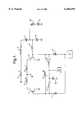
- FIG. 1illustrates a circuit diagram of a preferred embodiment of the present invention.
- FIG. 1circuit diagram of a preferred embodiment of the invention labelled FIG. 1.
- FIG. 1shows a drive circuit arrangement for a gas discharge lamp, comprising a self resonating inverter for providing a drive voltage across a load.
- the inverteris constituted by field effect transistors 1 and 2 which operate in anti-phase together with a first transformer comprising inductances 3, 4 and 5, the load 6 comprising an impedance having a reactive component and a capacitor 7 which forms a resonant circuit together with the load, components 8 and 9 which form part of a feedback loop and gate coupling components 10, 11 and 12.
- These gate coupling componentscomprise a tank circuit for cancelling the reactive component of the impedance of a load (6) coupled to the inverter in use.
- a voltage division circuitcomprising capacitors 7 and 8 provides a given fraction of the said drive voltage to the gates of the field effect transistors 1 and 2 in use.
- Phase shifting means for shifting the phase of the given fraction of the said drive voltageis provided by the inductance 9 feeding into the gate tank circuit.
- Diodes 13 and 14comprise a voltage limiter which acts to restrict the peak resonant voltage as explained below.
- the circuit arrangement of FIG. 1is also provided with an autobias circuit 15 which biases the transistor gates positive until the oscillation starts, and then returns the gate bias to zero, and an inhibit circuit 16 which pulls the cathodes of diodes 17 and 18 to ground when it is desired to stop the oscillations.
- the details of circuits 15 and 16are not shown as suitable implementations of both circuits are well known to those skilled in the art.
- the load impedance 6will in practice typically consist of a spiral coil having an inductance positioned adjacent a glass envelope containing a gas in which a glow discharge is to be maintained. Power absorbed by the discharge will cause the load impedance to have a corresponding resistive component.
- the inductive load 6 and capacitor 7are automatically driven close to resonance by the phase shifts in the circuit, and their values thus determine the operating frequency of the circuit arrangement.
- the resonant voltage across capacitor 7is divided down by the much larger capacitance of capacitor 8.
- the voltage across 8is proportional to the discharge running voltage. Since it is known that this voltage remains relatively constant over a wide range of powers it follows that the voltage across 8 also remains fairly constant over a wide range of supply voltages. Thus the voltage across 8 is suitable for driving the FET gates.
- phase shifts present in the circuit shown in FIG. 1 in operationare as follows:
- the adjustable inductor 10is part of the gate tank circuit, and is tuned or set such that the gate input appears resistive. It may, for example, be trimmed or adjusted on the circuit assembly line and need not be user adjustable. Since the effect of tuning it is to alter the power of the light source, it can conveniently be adjusted for a given or predetermined supply current.
- inductor 9If the inductor 9 is chosen such that the reactive component of its impedance is equal in magnitude to the resistance of the gate tank circuit, there will be a ⁇ /4 radian phase shift from capacitor 8 to the gate of transistor 2. This forces the loop phase from the secondary of Transformer 1 (i.e. inductance 5) to capacitor 8 to be 3 ⁇ /4 radians, under which condition the self oscillating inverter will automatically run at a higher frequency than the resonant frequency of components 6 and 7, with the drain load of the transistors appearing inductive. This is required to provide efficient switching of the transistors.
- a high gate Qis essential, and the lower the gate capacitance the better.
- a transient gate rating to 35Vis necessary.
- the transformercomprising windings 3, 4 and 5 used in prototype tests was trifilar wound.
- the two drain windingsare preferably bifilar wound; coupling to the third winding is less important.
- the coil used in the embodiment of FIG. 1had a Q of 220 at 10 Mhz.
- capacitor 7must have a high Q at 10 Mhz, whilst capacitor 8 must look like a high Q capacitor at 10 Mhz.
- Inductor 9 used for the prototypehad a Q of 200 and was wound on a Micrometals core. A much lower Q would also be acceptable.
- the adjustable inductor 10 used in the embodiment of FIG. 1comprised 6 turns of 0.4 mm diameter wire in a 2.5 cm coil, having a Q of 150. A much lower Q would be acceptable.
- the inventionhas particular application for lights powered by lead-acid or similar batteries, especially backlights for liquid crystal displays, or vehicle warning lights.
Landscapes
- Circuit Arrangements For Discharge Lamps (AREA)
- Inverter Devices (AREA)
Abstract
Description
TABLE 1 ______________________________________ Reference Numeral Component type Value/Serial Number ______________________________________ 1, 2 Power FET IRF510, 100 V, 0.5Ω 3, 4, 5 Transformer 1 Windings each 9 turns bifilar wound on 0.94 cm o.d 4C65 ferrite core 6Coil 12 turns of 0.4 mm PTFE covered wire wound on 28 mm diameter envelope. 7 Capacitor 47 pF, 6 kV,COG 8 Capacitor 1n5, 100 V, COG 9 Inductor 1.6μH 10 Adjustable Inductance 1.4 μH nominal 11, 12Transformer 2 Windings each 5 turns on 0.94 cm o.d.4C65 ferrite core 13, 14 Zener Diodes 30 V,low power 20 Capacitor 4.7 nF Ceramic ______________________________________
Claims (7)
Applications Claiming Priority (3)
| Application Number | Priority Date | Filing Date | Title |
|---|---|---|---|
| GB9702555 | 1997-02-07 | ||
| GB9702555AGB2322019A (en) | 1997-02-07 | 1997-02-07 | Gas discharge lamp drive circuit |
| PCT/GB1998/000257WO1998035537A1 (en) | 1997-02-07 | 1998-01-28 | A drive circuit arrangement for a gas discharge lamp |
Publications (1)
| Publication Number | Publication Date |
|---|---|
| US6166494Atrue US6166494A (en) | 2000-12-26 |
Family
ID=10807267
Family Applications (1)
| Application Number | Title | Priority Date | Filing Date |
|---|---|---|---|
| US09/355,841Expired - LifetimeUS6166494A (en) | 1997-02-07 | 1998-01-28 | Drive circuit arrangement for a gas discharge lamp |
Country Status (7)
| Country | Link |
|---|---|
| US (1) | US6166494A (en) |
| EP (1) | EP1013152B1 (en) |
| AU (1) | AU5774098A (en) |
| CA (1) | CA2280030A1 (en) |
| DE (1) | DE69806398T2 (en) |
| GB (2) | GB2322019A (en) |
| WO (1) | WO1998035537A1 (en) |
Cited By (8)
| Publication number | Priority date | Publication date | Assignee | Title |
|---|---|---|---|---|
| US6329865B1 (en)* | 1999-03-18 | 2001-12-11 | Maxim Integrated Products, Inc. | Linearized transconductance cell |
| US6825620B2 (en) | 1999-06-21 | 2004-11-30 | Access Business Group International Llc | Inductively coupled ballast circuit |
| US7118240B2 (en) | 1999-06-21 | 2006-10-10 | Access Business Group International Llc | Inductively powered apparatus |
| US7385357B2 (en) | 1999-06-21 | 2008-06-10 | Access Business Group International Llc | Inductively coupled ballast circuit |
| US7408324B2 (en) | 2004-10-27 | 2008-08-05 | Access Business Group International Llc | Implement rack and system for energizing implements |
| US7462951B1 (en) | 2004-08-11 | 2008-12-09 | Access Business Group International Llc | Portable inductive power station |
| US7612528B2 (en) | 1999-06-21 | 2009-11-03 | Access Business Group International Llc | Vehicle interface |
| WO2023149276A1 (en)* | 2022-02-07 | 2023-08-10 | ローム株式会社 | Semiconductor device |
Families Citing this family (4)
| Publication number | Priority date | Publication date | Assignee | Title |
|---|---|---|---|---|
| GB9923408D0 (en)* | 1999-10-05 | 1999-12-08 | Central Research Lab Ltd | A high frequency power oscillator |
| GB9923405D0 (en)* | 1999-10-05 | 1999-12-08 | Central Research Lab Ltd | A high frquency power oscillator |
| WO2001026430A1 (en)* | 1999-10-05 | 2001-04-12 | Central Research Laboratories Limited | A self-oscillating power supply circuit |
| EP1330943B1 (en)* | 2000-10-31 | 2011-01-05 | Osram Sylvania, Inc. | Ballast self oscillating inverter with phase controlled voltage feedback |
Citations (3)
| Publication number | Priority date | Publication date | Assignee | Title |
|---|---|---|---|---|
| US5574335A (en)* | 1994-08-02 | 1996-11-12 | Osram Sylvania Inc. | Ballast containing protection circuit for detecting rectification of arc discharge lamp |
| US5781418A (en)* | 1996-12-23 | 1998-07-14 | Philips Electronics North America Corporation | Switching scheme for power supply having a voltage-fed inverter |
| US6040661A (en)* | 1998-02-27 | 2000-03-21 | Lumion Corporation | Programmable universal lighting system |
Family Cites Families (7)
| Publication number | Priority date | Publication date | Assignee | Title |
|---|---|---|---|---|
| US4322789A (en)* | 1979-06-29 | 1982-03-30 | Mere, Malleray & Cie | Static converter of symmetrical type |
| JPH06111968A (en)* | 1992-09-29 | 1994-04-22 | Toshiba Lighting & Technol Corp | Electrodeless lamp lighting device |
| JPH0645082A (en)* | 1992-07-27 | 1994-02-18 | Matsushita Electric Works Ltd | Electrodeless discharge lamp lighting device |
| US5446350A (en)* | 1994-04-18 | 1995-08-29 | General Electric Company | Impedance matching circuit for an electrodeless fluorescent lamp ballast |
| US5406177A (en)* | 1994-04-18 | 1995-04-11 | General Electric Company | Gas discharge lamp ballast circuit with compact starting circuit |
| US5541829A (en)* | 1994-11-25 | 1996-07-30 | Matsushita Electric Works, Ltd. | Power source device |
| US5694007A (en)* | 1995-04-19 | 1997-12-02 | Systems And Services International, Inc. | Discharge lamp lighting system for avoiding high in-rush current |
- 1997
- 1997-02-07GBGB9702555Apatent/GB2322019A/ennot_activeWithdrawn
- 1998
- 1998-01-28WOPCT/GB1998/000257patent/WO1998035537A1/enactiveIP Right Grant
- 1998-01-28GBGB9918461Apatent/GB2336954A/ennot_activeWithdrawn
- 1998-01-28USUS09/355,841patent/US6166494A/ennot_activeExpired - Lifetime
- 1998-01-28CACA002280030Apatent/CA2280030A1/ennot_activeAbandoned
- 1998-01-28EPEP98901409Apatent/EP1013152B1/ennot_activeExpired - Lifetime
- 1998-01-28AUAU57740/98Apatent/AU5774098A/ennot_activeAbandoned
- 1998-01-28DEDE69806398Tpatent/DE69806398T2/ennot_activeExpired - Fee Related
Patent Citations (3)
| Publication number | Priority date | Publication date | Assignee | Title |
|---|---|---|---|---|
| US5574335A (en)* | 1994-08-02 | 1996-11-12 | Osram Sylvania Inc. | Ballast containing protection circuit for detecting rectification of arc discharge lamp |
| US5781418A (en)* | 1996-12-23 | 1998-07-14 | Philips Electronics North America Corporation | Switching scheme for power supply having a voltage-fed inverter |
| US6040661A (en)* | 1998-02-27 | 2000-03-21 | Lumion Corporation | Programmable universal lighting system |
Cited By (17)
| Publication number | Priority date | Publication date | Assignee | Title |
|---|---|---|---|---|
| US6329865B1 (en)* | 1999-03-18 | 2001-12-11 | Maxim Integrated Products, Inc. | Linearized transconductance cell |
| US7612528B2 (en) | 1999-06-21 | 2009-11-03 | Access Business Group International Llc | Vehicle interface |
| US7439684B2 (en) | 1999-06-21 | 2008-10-21 | Access Business Group International Llc | Inductive lamp assembly |
| US7126450B2 (en) | 1999-06-21 | 2006-10-24 | Access Business Group International Llc | Inductively powered apparatus |
| US7180248B2 (en) | 1999-06-21 | 2007-02-20 | Access Business Group International, Llc | Inductively coupled ballast circuit |
| US7233222B2 (en) | 1999-06-21 | 2007-06-19 | Access Business Group International Llc | Inductively powered apparatus |
| US7279843B2 (en) | 1999-06-21 | 2007-10-09 | Access Business Group International Llc | Inductively powered apparatus |
| US7118240B2 (en) | 1999-06-21 | 2006-10-10 | Access Business Group International Llc | Inductively powered apparatus |
| US7385357B2 (en) | 1999-06-21 | 2008-06-10 | Access Business Group International Llc | Inductively coupled ballast circuit |
| US7427839B2 (en) | 1999-06-21 | 2008-09-23 | Access Business Group International Llc | Inductively powered apparatus |
| US8138875B2 (en) | 1999-06-21 | 2012-03-20 | Access Business Group International Llc | Inductively powered apparatus |
| US7639110B2 (en) | 1999-06-21 | 2009-12-29 | Access Business Group International Llc | Inductively powered apparatus |
| US6825620B2 (en) | 1999-06-21 | 2004-11-30 | Access Business Group International Llc | Inductively coupled ballast circuit |
| US7615936B2 (en) | 1999-06-21 | 2009-11-10 | Access Business Group International Llc | Inductively powered apparatus |
| US7462951B1 (en) | 2004-08-11 | 2008-12-09 | Access Business Group International Llc | Portable inductive power station |
| US7408324B2 (en) | 2004-10-27 | 2008-08-05 | Access Business Group International Llc | Implement rack and system for energizing implements |
| WO2023149276A1 (en)* | 2022-02-07 | 2023-08-10 | ローム株式会社 | Semiconductor device |
Also Published As
| Publication number | Publication date |
|---|---|
| GB9918461D0 (en) | 1999-10-06 |
| GB9702555D0 (en) | 1997-03-26 |
| GB2336954A (en) | 1999-11-03 |
| AU5774098A (en) | 1998-08-26 |
| DE69806398D1 (en) | 2002-08-08 |
| EP1013152B1 (en) | 2002-07-03 |
| WO1998035537A1 (en) | 1998-08-13 |
| CA2280030A1 (en) | 1998-08-13 |
| GB2322019A (en) | 1998-08-12 |
| EP1013152A1 (en) | 2000-06-28 |
| DE69806398T2 (en) | 2003-03-06 |
Similar Documents
| Publication | Publication Date | Title |
|---|---|---|
| US4631449A (en) | Integral crystal-controlled line-voltage ballast for compact RF fluorescent lamps | |
| US3753071A (en) | Low cost transistorized inverter | |
| KR100443300B1 (en) | Circuit for operating an electrodeless low-pressure discharge lamp | |
| US5084652A (en) | Fluorescent lamp lighting apparatus | |
| US4560908A (en) | High-frequency oscillator-inverter ballast circuit for discharge lamps | |
| US5341068A (en) | Electronic ballast arrangement for a compact fluorescent lamp | |
| US6166494A (en) | Drive circuit arrangement for a gas discharge lamp | |
| JPH0557726B2 (en) | ||
| EP0202579A1 (en) | Power feed apparatus for load having reverse blocking characteristics | |
| US5557176A (en) | Modulated electronic ballast for driving gas discharge lamps | |
| US4701671A (en) | High-frequency oscillator-inverter ballast circuit for discharge lamps | |
| US5495404A (en) | Multi-resonant inverter | |
| GB2204751A (en) | Discharge lamp circuits | |
| US6144173A (en) | Single switch electronic ballast | |
| GB2309344A (en) | HF FET oscillator for electrodeless backlight | |
| KR940009873B1 (en) | Inverter | |
| EP1228672B1 (en) | A power oscillator for driving a discharge lamp | |
| US5786670A (en) | High-frequency converter for fluorescent lamps using an improved trigger circuit | |
| US20020167281A1 (en) | Circuit arrangement | |
| KR920004995B1 (en) | Arrangements for discharge lamps | |
| JP3713129B2 (en) | Discharge lamp lighting device | |
| GB2379098A (en) | Tunable capacitive load driver for electroluminescent lamp | |
| KR920006437Y1 (en) | Neon lamp lighting device | |
| JPH0785661B2 (en) | Inverter device | |
| WO2002030160A1 (en) | A power supply for driving a discharge lamp |
Legal Events
| Date | Code | Title | Description |
|---|---|---|---|
| AS | Assignment | Owner name:CENTRAL RESEARCH LABORATORIES LIMITED, ENGLAND Free format text:ASSIGNMENT OF ASSIGNORS INTEREST;ASSIGNOR:GRENN, IAN M.;REEL/FRAME:010657/0021 Effective date:19990810 | |
| AS | Assignment | Owner name:CENTRAL RESEARCH LABORATORIES LIMITED, ENGLAND Free format text:CORRECTIVE ASSIGNMENT TO CORRECT INVENTOR'S SURNAME PREVIOUSLY RECORDED AT REEL 010657, FRAME 0021;ASSIGNOR:GREEN, IAN MACDONALD;REEL/FRAME:010644/0075 Effective date:19990810 Owner name:CENTRAL RESEARCH LABORATORIES LIMITED, ENGLAND Free format text:INVALID ASSIGNMENT.;ASSIGNOR:GREEN, IAN MACDONALD;REEL/FRAME:010534/0185 Effective date:19990810 | |
| STCF | Information on status: patent grant | Free format text:PATENTED CASE | |
| AS | Assignment | Owner name:CHI MEI OPTOELECTRONICS CORPORATION, TAIWAN Free format text:ASSIGNMENT OF ASSIGNORS INTEREST;ASSIGNOR:CENTRAL RESEARCH LABORATORIES LIMITED;REEL/FRAME:013691/0447 Effective date:20021127 | |
| FEPP | Fee payment procedure | Free format text:PAYOR NUMBER ASSIGNED (ORIGINAL EVENT CODE: ASPN); ENTITY STATUS OF PATENT OWNER: LARGE ENTITY | |
| FPAY | Fee payment | Year of fee payment:4 | |
| FPAY | Fee payment | Year of fee payment:8 | |
| AS | Assignment | Owner name:CHIMEI INNOLUX CORPORATION,TAIWAN Free format text:MERGER;ASSIGNOR:CHI MEI OPTOELECTRONICS CORP.;REEL/FRAME:024358/0221 Effective date:20100318 Owner name:CHIMEI INNOLUX CORPORATION, TAIWAN Free format text:MERGER;ASSIGNOR:CHI MEI OPTOELECTRONICS CORP.;REEL/FRAME:024358/0221 Effective date:20100318 | |
| FEPP | Fee payment procedure | Free format text:PAYOR NUMBER ASSIGNED (ORIGINAL EVENT CODE: ASPN); ENTITY STATUS OF PATENT OWNER: LARGE ENTITY Free format text:PAYER NUMBER DE-ASSIGNED (ORIGINAL EVENT CODE: RMPN); ENTITY STATUS OF PATENT OWNER: LARGE ENTITY | |
| FPAY | Fee payment | Year of fee payment:12 | |
| AS | Assignment | Owner name:INNOLUX CORPORATION, TAIWAN Free format text:CHANGE OF NAME;ASSIGNOR:CHIMEI INNOLUX CORPORATION;REEL/FRAME:032589/0585 Effective date:20121219 |