US6166417A - Complementary metal gates and a process for implementation - Google Patents
Complementary metal gates and a process for implementationDownload PDFInfo
- Publication number
- US6166417A US6166417AUS09/109,993US10999398AUS6166417AUS 6166417 AUS6166417 AUS 6166417AUS 10999398 AUS10999398 AUS 10999398AUS 6166417 AUS6166417 AUS 6166417A
- Authority
- US
- United States
- Prior art keywords
- gate electrode
- metal
- barrier layer
- type
- work function
- Prior art date
- Legal status (The legal status is an assumption and is not a legal conclusion. Google has not performed a legal analysis and makes no representation as to the accuracy of the status listed.)
- Expired - Lifetime
Links
Images


Classifications
- H—ELECTRICITY
- H10—SEMICONDUCTOR DEVICES; ELECTRIC SOLID-STATE DEVICES NOT OTHERWISE PROVIDED FOR
- H10D—INORGANIC ELECTRIC SEMICONDUCTOR DEVICES
- H10D64/00—Electrodes of devices having potential barriers
- H10D64/60—Electrodes characterised by their materials
- H10D64/66—Electrodes having a conductor capacitively coupled to a semiconductor by an insulator, e.g. MIS electrodes
- H10D64/661—Electrodes having a conductor capacitively coupled to a semiconductor by an insulator, e.g. MIS electrodes the conductor comprising a layer of silicon contacting the insulator, e.g. polysilicon having vertical doping variation
- H10D64/662—Electrodes having a conductor capacitively coupled to a semiconductor by an insulator, e.g. MIS electrodes the conductor comprising a layer of silicon contacting the insulator, e.g. polysilicon having vertical doping variation the conductor further comprising additional layers, e.g. multiple silicon layers having different crystal structures
- H10D64/664—Electrodes having a conductor capacitively coupled to a semiconductor by an insulator, e.g. MIS electrodes the conductor comprising a layer of silicon contacting the insulator, e.g. polysilicon having vertical doping variation the conductor further comprising additional layers, e.g. multiple silicon layers having different crystal structures the additional layers comprising a barrier layer between the layer of silicon and an upper metal or metal silicide layer
- H—ELECTRICITY
- H01—ELECTRIC ELEMENTS
- H01L—SEMICONDUCTOR DEVICES NOT COVERED BY CLASS H10
- H01L21/00—Processes or apparatus adapted for the manufacture or treatment of semiconductor or solid state devices or of parts thereof
- H01L21/02—Manufacture or treatment of semiconductor devices or of parts thereof
- H01L21/04—Manufacture or treatment of semiconductor devices or of parts thereof the devices having potential barriers, e.g. a PN junction, depletion layer or carrier concentration layer
- H01L21/18—Manufacture or treatment of semiconductor devices or of parts thereof the devices having potential barriers, e.g. a PN junction, depletion layer or carrier concentration layer the devices having semiconductor bodies comprising elements of Group IV of the Periodic Table or AIIIBV compounds with or without impurities, e.g. doping materials
- H01L21/28—Manufacture of electrodes on semiconductor bodies using processes or apparatus not provided for in groups H01L21/20 - H01L21/268
- H01L21/28008—Making conductor-insulator-semiconductor electrodes
- H01L21/28017—Making conductor-insulator-semiconductor electrodes the insulator being formed after the semiconductor body, the semiconductor being silicon
- H01L21/28026—Making conductor-insulator-semiconductor electrodes the insulator being formed after the semiconductor body, the semiconductor being silicon characterised by the conductor
- H01L21/28088—Making conductor-insulator-semiconductor electrodes the insulator being formed after the semiconductor body, the semiconductor being silicon characterised by the conductor the final conductor layer next to the insulator being a composite, e.g. TiN
- H—ELECTRICITY
- H10—SEMICONDUCTOR DEVICES; ELECTRIC SOLID-STATE DEVICES NOT OTHERWISE PROVIDED FOR
- H10D—INORGANIC ELECTRIC SEMICONDUCTOR DEVICES
- H10D84/00—Integrated devices formed in or on semiconductor substrates that comprise only semiconducting layers, e.g. on Si wafers or on GaAs-on-Si wafers
- H10D84/01—Manufacture or treatment
- H10D84/0123—Integrating together multiple components covered by H10D12/00 or H10D30/00, e.g. integrating multiple IGBTs
- H10D84/0126—Integrating together multiple components covered by H10D12/00 or H10D30/00, e.g. integrating multiple IGBTs the components including insulated gates, e.g. IGFETs
- H10D84/0165—Integrating together multiple components covered by H10D12/00 or H10D30/00, e.g. integrating multiple IGBTs the components including insulated gates, e.g. IGFETs the components including complementary IGFETs, e.g. CMOS devices
- H10D84/0172—Manufacturing their gate conductors
- H10D84/0177—Manufacturing their gate conductors the gate conductors having different materials or different implants
- H—ELECTRICITY
- H10—SEMICONDUCTOR DEVICES; ELECTRIC SOLID-STATE DEVICES NOT OTHERWISE PROVIDED FOR
- H10D—INORGANIC ELECTRIC SEMICONDUCTOR DEVICES
- H10D84/00—Integrated devices formed in or on semiconductor substrates that comprise only semiconducting layers, e.g. on Si wafers or on GaAs-on-Si wafers
- H10D84/01—Manufacture or treatment
- H10D84/02—Manufacture or treatment characterised by using material-based technologies
- H10D84/03—Manufacture or treatment characterised by using material-based technologies using Group IV technology, e.g. silicon technology or silicon-carbide [SiC] technology
- H10D84/038—Manufacture or treatment characterised by using material-based technologies using Group IV technology, e.g. silicon technology or silicon-carbide [SiC] technology using silicon technology, e.g. SiGe
Definitions
- the inventionrelates to integrated circuit devices and more particularly to complementary metal gate devices.
- a metal gate electrodehas distinct advantages over a polysilicon gate for current and future technologies of high performance integrated circuit devices.
- a gate electrode of polysiliconwill generally experience a depletion of carriers in the area of the polysilicon near the gate dielectric resulting in a reduced electric field at the surface of the semiconductor.
- the polysilicon depletion effectis not as significant with gate dielectrics having thicknesses of 50 ⁇ or more.
- the contribution of the voltage drop at inversion due to the role of the polysilicon depletion effect on device performancewill be important.
- the polysilicon depletion effectmust be accounted for in device scaling.
- a metal gate electrodedoes not suffer from the depletion effect associated with a polysilicon gate electrode.
- a metal gate electrodealso reduces the parasitic resistance of a gate electrode line to accommodate the use of longer gate electrodes in integrated circuit design for applications such as stacked gates, word lines, buffer drivers, etc. Longer gate electrodes generally correspond to field effect transistors of greater width.
- a semiconductor such as siliconhas a certain energy level measured conventionally by its Fermi level.
- the Fermi level of a materialdetermines its work function.
- the intrinsic Fermi level of an undoped semiconductoris at the middle of the bandgap between the conduction and valence band edges.
- the Fermi levelis closer to the conduction band than to the valence band (e.g., about 4.15 electron-volts).
- the Fermi levelis closer to the valence band than the conduction band (e.g., about 5.2 electron-volts).
- Metals, metal alloys, metal silicides, metal nitrides, and metal oxideshave been identified that have work functions similar to the work function of a conventional P-type doped semiconductor substrate and of a conventional N-type doped semiconductor substrate.
- metals that have a work function similar to a P-type doped semiconductor materialinclude but are not limited to, nickel (Ni), Ruthenium oxide (RuO), and molybdenum nitride (MoN).
- metalsthat have a work function similar to an N-type doped semiconductor material, include but are not limited to, ruthenium (Ru), zirconium (Zr), niobium (Nb), tantalum (Ta), and titanium silicide (TiSi 2 ).
- CMOScomplementary metal oxide semiconductor
- mid-bandgape.g., Fermi level located in the middle of the conduction and valence band of a silicon substrate
- V Tsmall threshold voltage
- a transistor deviceincludes a gate dielectric overlying a substrate, a barrier layer overlying the gate dielectric, and a gate electrode overlying the barrier layer.
- the barrier layer of the devicehas a physical property that inhibits interaction between the gate dielectric and the gate electrode.
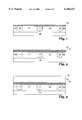
- FIG. 1is a schematic illustration of a side view of a semiconductor substrate having isolated regions having an NMOS and PMOS device, respectively, and a gate dielectric layer overlying the substrate in accordance with an embodiment of the invention.
- FIG. 2shows the substrate of FIG. 1 after the further processing step of forming a barrier layer overlying the gate dielectric layer in accordance with an embodiment of the invention.
- FIG. 3shows the substrate of FIG. 1 after the further processing step of depositing an N-type metal layer over the barrier layer in accordance with an embodiment of the invention.
- FIG. 4shows the substrate of FIG. 1 after the further processing step of patterning a photoresist over the N-type metal layer in an area identified for an N-type device in accordance with an embodiment of the invention.
- FIG. 5shows the substrate of FIG. 1 after the further processing step of removing N-type material in all areas of the substrate except those identified for an N-type device and the removal of any photoresist protecting the N-type metal in accordance with an embodiment of the invention.
- FIG. 6shows the substrate of FIG. 1 after the further processing of depositing a P-type metal over the substrate in accordance with an embodiment of the invention.
- FIG. 7shows the substrate of FIG. 1 after the further processing step of planarizing the P-type metal to the N-type metal in accordance with an embodiment of the invention.
- FIG. 8shows the substrate of FIG. 1 after the further processing step of forming N-type and P-type gate devices in their respective areas in accordance with an embodiment of the invention.
- FIG. 9shows the substrate of FIG. 1 after the further processing step of forming complementary diffusion or junction regions in the substrate adjacent the N-type gate electrode and the P-type gate electrode, respectively, in accordance with an embodiment of the invention.
- An apparatus employing metal gate electrodes tuned for or having a work function similar to the desired device typeis disclosed.
- the inventionis particularly useful for, but not limited to, the utilization of metal gate electrodes in CMOS technology tuned for optimum NMOS and PMOS device performance.
- the inventionoffers a workable process for providing integrated complementary metal gate electrode technology that does not damage the gate dielectric during patterning.
- FIGS. 1-9illustrate an embodiment of a method of forming PMOS and CMOS devices utilizing the complementary metal gate technology of the invention.
- FIG. 1shows a semiconductor substrate 100 having shallow trench isolation structures 110 formed in substrate 100, such as a silicon substrate.
- shallow trench isolation structures 110define regions or areas for individual transistor devices.
- FIG. 1also shows the formation of wells 105 and 115 in the individual regions or areas defined by shallow trench isolation structures 110.
- P-type well 105is formed in one region of substrate 100 while N-type well 115 is formed in a second region of substrate 100.
- the P-type wellis formed by introducing a dopant, such as boron into the substrate.
- N-type well 115is formed by introducing a dopant, such as arsenic, phosphorous, or antimony into substrate 100.
- a dopantsuch as arsenic, phosphorous, or antimony.
- FIG. 1also shows substrate 100 after the further processing step of forming a gate dielectric over the surface of substrate 100.
- the gate dielectricmay be grown or deposited.
- An example of a gate dielectric that is typically grown by thermal techniques over substrate 100is silicon dioxide (SiO 2 ). It is to be appreciated that other gate dielectrics may also be used to further optimize the NMOS and PMOS devices. For example, gate dielectrics having a high dielectric constant design may be utilized in an appropriate manner as known in the art.
- FIG. 2shows a substrate of FIG. 1 after the further processing step of depositing barrier layer 125 over gate dielectic 120.
- Barrier layer 125is of a material that prevents an interaction between gate dielectric 120 and a subsequently deposited metal for a metal gate electrode. Barrier layer 125 also acts as an etch-stop during subsequent processing to protect gate dielectric 120 from being destroyed by an etch patterning of a gate electrode.
- barrier layer 125has a thicknes on the order of, for example, 5 to 200 ⁇ .
- the material chosen for barrier layer 125in one embodiment, has a low density of states (e.g., small amount of free carriers). In this manner, the low density of states of the material allows the barrier layer 125 to be pinned or controlled by an overlying metal gate electrode.
- the thickness of barrier layer 125is less than a critical thickness determined by the density of states of the barrier layer (e.g., a thickness in which the carriers in the barrier layer will effect the work function of the gate electrode stack-barrier layer plus metal layer). The lower the charge density of the density of states, the greater the critical thickness of barrier layer 125.
- barrier layer plus metal layerthe work function of the gate electrode stack (i.e., barrier layer plus metal layer) is determined by the metal layer and not the barrier layer.
- suitable barrier layersinclude, but are not limited to, undoped polysilicon, titanium nitride (TiN), tantalum nitride (TaN), and tantalum silicon nitride (TaSiN).
- FIG. 3shows substrate 100 after the further processing step of depositing metal layer 130, such as for example, an N-type metal layer or a P-type metal layer.
- Metal layer 130is deposited to a desired gate electrode thickness suitable for the integrated circuit device characteristics.
- metal layerBy describing metal layer as either N-type or P-type, it is meant that the metal has a work function optimized for either an NMOS or a PMOS device. In other words, the work function of the metal layer is close to that of a corresponding Fermi level N-type doped polysilicon (e.g., 4.15 electron-volts) or P-type doped polysilicon (e.g., 5.2 electron-volts).
- the inventiondescribes metals having close to the corresponding Fermi level of either N-type or P-type doped polysilicon. It is to be appreciated that the suitable metal may exist at the desired work function in its natural state or by chemical reaction, alloying, doping, etc.
- FIG. 3is described as depositing an N-type metal layer 130 such as, for example, TiSi 2 , over substrate 100 and the remainder will proceed on that assumption. It is to be appreciated, however, that the method of the invention is not to be limited to a process restricting the order of the deposition of optimized metal materials.
- FIG. 4shows substrate 100 after the further processing step of patterning photoresist layer 133 over a portion of metal layer 130.
- photoresist layer 133is patterned over a portion of metal layer 130 identified with P-type well 105, implying that the area or cell region above P-type well 105 will incorporate an N-type device.
- Photoresist layer 133may be patterned by techniques known in the art such as applying a light-sensitive material over N-type metal layer 130, exposing the material over the area associated with P-type well 105, and removing the unexposed material. It is to be appreciated that photoresist layer 133 serves as a masking layer.
- the scope of the method of the inventionshould not be limited by the use of photoresist material as the masking layer, but should contemplate other masking layers, such as, for example, dielectrics and other materials.
- photoresist layer 133protects the entirety of the device region or cell region occupied by P-type well 105. In this manner, photoresist layer 135 extends from shallow trench isolation structures 110 between the device region.
- FIG. 5shows substrate 100 after the further processing step of etching metal layer 130 with a suitable etchant (such as a chlorine-chemistry etchant) and removing photoresist layer 133. Metal layer 130 is removed from all areas except the area above P-type well 105.
- a suitable etchantsuch as a chlorine-chemistry etchant
- the etch of metal layer 130removes metal layer 130 material from all areas of substrate 100 except for those areas protected by photoresist layer 133.
- the etch of metal layer 130stops at barrier layer 125. In this manner, gate dielectric layer 120 is not damaged.
- Barrier layer 125functions as an etch stop to protect gate dielectric layer 120.
- FIG. 6shows substrate 100 after the further processing step of removing photoresist layer 133 and depositing a complementary metal, in this case P-type metal layer 135 over substrate 100.
- P-type metal layer 135is conformally deposited over the surface of substrate 100 in that the thickness of metal layer 135 is consistent throughout and conforms to the topography of the surface of substrate 100.
- the thickness of P-type metal layeris chosen according to the desired device characteristics.
- An example of metals suitable as P-type metal layer 135includes, but is not limited to, MoSi 2 . These metal materials have work functions close to that corresponding to the Fermi level of P-type doped polysilicon (e.g., 5.2 electron-volts).
- FIG. 7shows substrate 100 after the further processing step of planarizing P-type metal layer 135 to N-type metal layer 130.
- the planarizationmay be accomplished by the use of a chemical-mechanical polish suitable for polishing metal layer 135.
- P-type metal layer 135is planarized to N-type metal layer 130.
- the planarization of P-type metal layer 135proceeds until the polishing contacts N-type metal layer 130 and the polishing is stopped.
- the N-type metal layer 130acts as a polishing stop.
- FIG. 8shows substrate 100 after the further processing step of etching (such as, for example, with a chorine-chemistry etchant) the individual metal layers 130 and 135 over their respective device regions.
- N-type metal layer 130is formed into metal gate electrode 130 over the region of substrate 100 occupied by P-type well 105.
- P-type metal layer 135is patterned into P-type gate electrode 135 over an area of substrate 100 occupied by N-type well 115.
- the lateral width of the individual N-type gate electrode 130 and P-type gate electrode 135are selected in accordance with the desired characteristics of the NMOS and PMOS device.
- Patterned in accordance with electrodes 130 and 135are barrier layer 125 and gate dielectric 120.
- a suitable etchant to pattern a barrier layer of undoped polysiliconis, for example, a CF 4 chemistry. This same etchant may be used to pattern the relatively thin gate dielectric layer 120.
- FIG. 9shows substrate 100 after the further processing step of forming diffusion or junction regions in substrate 100 in accordance with the characteristics of the desired device.
- the diffusion or junction regionswill have work functions similar to the metal gate electrode 130 and 135, respectively.
- N-type diffusion or junction regions 140are formed in P-well 105 in accordance with conventional techniques.
- N-type or junction regionsmay be formed adjacent the gate electrode and self-aligned to the gate by implanting a suitable dopant, such as, for example, arsenic, phosphorous, or antimony, into P-well 105.
- CMOS inverterSimilar processing steps may be used to form P-type diffusion or junction regions 145, using a dopant, such as, for example, boron. Pocket dopants may also be added at this point if desired.
- gate isolation spacers 150 of a suitable dielectricmay be incorporated around gate electrode 130 and gate electrode 135 to insulate the individual electrodes of the complementary transistor devices. The individual devices may then be connected in a conventional manner, if desired, to form a CMOS device (e.g., a CMOS inverter).
Landscapes
- Engineering & Computer Science (AREA)
- Chemical & Material Sciences (AREA)
- Composite Materials (AREA)
- Physics & Mathematics (AREA)
- Condensed Matter Physics & Semiconductors (AREA)
- General Physics & Mathematics (AREA)
- Manufacturing & Machinery (AREA)
- Computer Hardware Design (AREA)
- Microelectronics & Electronic Packaging (AREA)
- Power Engineering (AREA)
- Metal-Oxide And Bipolar Metal-Oxide Semiconductor Integrated Circuits (AREA)
- Electrodes Of Semiconductors (AREA)
Abstract
Description
1. Field of the Invention
In the context of insulated gate field effect transistors, the invention relates to integrated circuit devices and more particularly to complementary metal gate devices.
2. Background Information
A metal gate electrode has distinct advantages over a polysilicon gate for current and future technologies of high performance integrated circuit devices. At inversion, a gate electrode of polysilicon, for example, will generally experience a depletion of carriers in the area of the polysilicon near the gate dielectric resulting in a reduced electric field at the surface of the semiconductor. The polysilicon depletion effect is not as significant with gate dielectrics having thicknesses of 50 Å or more. However, as gate dielectric thicknesses decrease, the contribution of the voltage drop at inversion due to the role of the polysilicon depletion effect on device performance will be important. Thus, the polysilicon depletion effect must be accounted for in device scaling. A metal gate electrode does not suffer from the depletion effect associated with a polysilicon gate electrode. A metal gate electrode also reduces the parasitic resistance of a gate electrode line to accommodate the use of longer gate electrodes in integrated circuit design for applications such as stacked gates, word lines, buffer drivers, etc. Longer gate electrodes generally correspond to field effect transistors of greater width.
A semiconductor such as silicon has a certain energy level measured conventionally by its Fermi level. The Fermi level of a material determines its work function. The intrinsic Fermi level of an undoped semiconductor is at the middle of the bandgap between the conduction and valence band edges. In an N-type doped silicon, the Fermi level is closer to the conduction band than to the valence band (e.g., about 4.15 electron-volts). In a P-type doped silicon, the Fermi level is closer to the valence band than the conduction band (e.g., about 5.2 electron-volts).
Metals, metal alloys, metal silicides, metal nitrides, and metal oxides (collectively herein "metals") have been identified that have work functions similar to the work function of a conventional P-type doped semiconductor substrate and of a conventional N-type doped semiconductor substrate. Examples of metals that have a work function similar to a P-type doped semiconductor material, include but are not limited to, nickel (Ni), Ruthenium oxide (RuO), and molybdenum nitride (MoN). Examples of metals that have a work function similar to an N-type doped semiconductor material, include but are not limited to, ruthenium (Ru), zirconium (Zr), niobium (Nb), tantalum (Ta), and titanium silicide (TiSi2).
Prior art metal gate electrodes are used in complementary metal oxide semiconductor (CMOS) technology in the form of mid-bandgap (e.g., Fermi level located in the middle of the conduction and valence band of a silicon substrate) metal gate electrodes to maintain the symmetry between NMOS and PMOS devices. The shortcoming of the mid-bandgap metal technique is that a mid-bandgap metal cannot deliver the small threshold voltage (VT) necessary for future technologies without degrading short channel effects. To date, however, a complementary metal gate approach with individual work functions optimized for both NMOS and PMOS devices has not been integrated into a workable process. The simple method to deposit complementary metals damages the underlying thin gate dielectrics during patterning, making the transistor with the damaged gate dielectric unusable.
What is needed is a method of utilizing complementary metal gate electrode technology in CMOS circuits.
A transistor device is disclosed. The transistor device includes a gate dielectric overlying a substrate, a barrier layer overlying the gate dielectric, and a gate electrode overlying the barrier layer. The barrier layer of the device has a physical property that inhibits interaction between the gate dielectric and the gate electrode.
FIG. 1 is a schematic illustration of a side view of a semiconductor substrate having isolated regions having an NMOS and PMOS device, respectively, and a gate dielectric layer overlying the substrate in accordance with an embodiment of the invention.
FIG. 2 shows the substrate of FIG. 1 after the further processing step of forming a barrier layer overlying the gate dielectric layer in accordance with an embodiment of the invention.
FIG. 3 shows the substrate of FIG. 1 after the further processing step of depositing an N-type metal layer over the barrier layer in accordance with an embodiment of the invention.
FIG. 4 shows the substrate of FIG. 1 after the further processing step of patterning a photoresist over the N-type metal layer in an area identified for an N-type device in accordance with an embodiment of the invention.
FIG. 5 shows the substrate of FIG. 1 after the further processing step of removing N-type material in all areas of the substrate except those identified for an N-type device and the removal of any photoresist protecting the N-type metal in accordance with an embodiment of the invention.
FIG. 6 shows the substrate of FIG. 1 after the further processing of depositing a P-type metal over the substrate in accordance with an embodiment of the invention.
FIG. 7 shows the substrate of FIG. 1 after the further processing step of planarizing the P-type metal to the N-type metal in accordance with an embodiment of the invention.
FIG. 8 shows the substrate of FIG. 1 after the further processing step of forming N-type and P-type gate devices in their respective areas in accordance with an embodiment of the invention.
FIG. 9 shows the substrate of FIG. 1 after the further processing step of forming complementary diffusion or junction regions in the substrate adjacent the N-type gate electrode and the P-type gate electrode, respectively, in accordance with an embodiment of the invention.
An apparatus employing metal gate electrodes tuned for or having a work function similar to the desired device type is disclosed. The invention is particularly useful for, but not limited to, the utilization of metal gate electrodes in CMOS technology tuned for optimum NMOS and PMOS device performance. The invention offers a workable process for providing integrated complementary metal gate electrode technology that does not damage the gate dielectric during patterning.
FIGS. 1-9 illustrate an embodiment of a method of forming PMOS and CMOS devices utilizing the complementary metal gate technology of the invention. FIG. 1 shows asemiconductor substrate 100 having shallowtrench isolation structures 110 formed insubstrate 100, such as a silicon substrate. In this embodiment, shallowtrench isolation structures 110 define regions or areas for individual transistor devices. FIG. 1 also shows the formation ofwells trench isolation structures 110. For example, P-type well 105 is formed in one region ofsubstrate 100 while N-type well 115 is formed in a second region ofsubstrate 100. The P-type well is formed by introducing a dopant, such as boron into the substrate. N-type well 115 is formed by introducing a dopant, such as arsenic, phosphorous, or antimony intosubstrate 100. The practice of forming shallowtrench isolation structures 110 andwells
FIG. 1 also showssubstrate 100 after the further processing step of forming a gate dielectric over the surface ofsubstrate 100. The gate dielectric may be grown or deposited. An example of a gate dielectric that is typically grown by thermal techniques oversubstrate 100 is silicon dioxide (SiO2). It is to be appreciated that other gate dielectrics may also be used to further optimize the NMOS and PMOS devices. For example, gate dielectrics having a high dielectric constant design may be utilized in an appropriate manner as known in the art.
After gate dielectric 120 is formed, FIG. 2 shows a substrate of FIG. 1 after the further processing step of depositingbarrier layer 125 over gate dielectic 120.Barrier layer 125 is of a material that prevents an interaction between gate dielectric 120 and a subsequently deposited metal for a metal gate electrode.Barrier layer 125 also acts as an etch-stop during subsequent processing to protect gate dielectric 120 from being destroyed by an etch patterning of a gate electrode.
In one embodiment,barrier layer 125 has a thicknes on the order of, for example, 5 to 200 Å. The material chosen forbarrier layer 125, in one embodiment, has a low density of states (e.g., small amount of free carriers). In this manner, the low density of states of the material allows thebarrier layer 125 to be pinned or controlled by an overlying metal gate electrode. In one embodiment, the thickness ofbarrier layer 125 is less than a critical thickness determined by the density of states of the barrier layer (e.g., a thickness in which the carriers in the barrier layer will effect the work function of the gate electrode stack-barrier layer plus metal layer). The lower the charge density of the density of states, the greater the critical thickness ofbarrier layer 125. In this manner, the work function of the gate electrode stack (i.e., barrier layer plus metal layer) is determined by the metal layer and not the barrier layer. Examples of suitable barrier layers include, but are not limited to, undoped polysilicon, titanium nitride (TiN), tantalum nitride (TaN), and tantalum silicon nitride (TaSiN).
FIG. 3 showssubstrate 100 after the further processing step of depositingmetal layer 130, such as for example, an N-type metal layer or a P-type metal layer.Metal layer 130 is deposited to a desired gate electrode thickness suitable for the integrated circuit device characteristics. By describing metal layer as either N-type or P-type, it is meant that the metal has a work function optimized for either an NMOS or a PMOS device. In other words, the work function of the metal layer is close to that of a corresponding Fermi level N-type doped polysilicon (e.g., 4.15 electron-volts) or P-type doped polysilicon (e.g., 5.2 electron-volts).
The invention describes metals having close to the corresponding Fermi level of either N-type or P-type doped polysilicon. It is to be appreciated that the suitable metal may exist at the desired work function in its natural state or by chemical reaction, alloying, doping, etc. In this embodiment, FIG. 3 is described as depositing an N-type metal layer 130 such as, for example, TiSi2, oversubstrate 100 and the remainder will proceed on that assumption. It is to be appreciated, however, that the method of the invention is not to be limited to a process restricting the order of the deposition of optimized metal materials.
FIG. 4 showssubstrate 100 after the further processing step of patterningphotoresist layer 133 over a portion ofmetal layer 130. In FIG. 4,photoresist layer 133 is patterned over a portion ofmetal layer 130 identified with P-type well 105, implying that the area or cell region above P-type well 105 will incorporate an N-type device.Photoresist layer 133 may be patterned by techniques known in the art such as applying a light-sensitive material over N-type metal layer 130, exposing the material over the area associated with P-type well 105, and removing the unexposed material. It is to be appreciated thatphotoresist layer 133 serves as a masking layer. The scope of the method of the invention should not be limited by the use of photoresist material as the masking layer, but should contemplate other masking layers, such as, for example, dielectrics and other materials.
As shown in FIG. 4,photoresist layer 133 protects the entirety of the device region or cell region occupied by P-type well 105. In this manner,photoresist layer 135 extends from shallowtrench isolation structures 110 between the device region. FIG. 5 showssubstrate 100 after the further processing step of etchingmetal layer 130 with a suitable etchant (such as a chlorine-chemistry etchant) and removingphotoresist layer 133.Metal layer 130 is removed from all areas except the area above P-type well 105.
As shown in FIG. 5, the etch ofmetal layer 130 removesmetal layer 130 material from all areas ofsubstrate 100 except for those areas protected byphotoresist layer 133. The etch ofmetal layer 130 stops atbarrier layer 125. In this manner,gate dielectric layer 120 is not damaged.Barrier layer 125 functions as an etch stop to protectgate dielectric layer 120.
FIG. 6 showssubstrate 100 after the further processing step of removingphotoresist layer 133 and depositing a complementary metal, in this case P-type metal layer 135 oversubstrate 100. P-type metal layer 135 is conformally deposited over the surface ofsubstrate 100 in that the thickness ofmetal layer 135 is consistent throughout and conforms to the topography of the surface ofsubstrate 100. The thickness of P-type metal layer is chosen according to the desired device characteristics. An example of metals suitable as P-type metal layer 135 includes, but is not limited to, MoSi2. These metal materials have work functions close to that corresponding to the Fermi level of P-type doped polysilicon (e.g., 5.2 electron-volts).
FIG. 7 showssubstrate 100 after the further processing step of planarizing P-type metal layer 135 to N-type metal layer 130. The planarization may be accomplished by the use of a chemical-mechanical polish suitable for polishingmetal layer 135. As shown in FIG. 7, P-type metal layer 135 is planarized to N-type metal layer 130. In other words, the planarization of P-type metal layer 135 proceeds until the polishing contacts N-type metal layer 130 and the polishing is stopped. Thus, the N-type metal layer 130 acts as a polishing stop.
FIG. 8 showssubstrate 100 after the further processing step of etching (such as, for example, with a chorine-chemistry etchant) theindividual metal layers type metal layer 130 is formed intometal gate electrode 130 over the region ofsubstrate 100 occupied by P-type well 105. P-type metal layer 135 is patterned into P-type gate electrode 135 over an area ofsubstrate 100 occupied by N-type well 115. The lateral width of the individual N-type gate electrode 130 and P-type gate electrode 135 are selected in accordance with the desired characteristics of the NMOS and PMOS device. Patterned in accordance withelectrodes barrier layer 125 andgate dielectric 120. A suitable etchant to pattern a barrier layer of undoped polysilicon is, for example, a CF4 chemistry. This same etchant may be used to pattern the relatively thingate dielectric layer 120.
FIG. 9 showssubstrate 100 after the further processing step of forming diffusion or junction regions insubstrate 100 in accordance with the characteristics of the desired device. In one embodiment, the diffusion or junction regions will have work functions similar to themetal gate electrode type gate electrode 130 overlying P-type well 105, N-type diffusion orjunction regions 140 are formed in P-well 105 in accordance with conventional techniques. For example, N-type or junction regions may be formed adjacent the gate electrode and self-aligned to the gate by implanting a suitable dopant, such as, for example, arsenic, phosphorous, or antimony, into P-well 105. Similar processing steps may be used to form P-type diffusion orjunction regions 145, using a dopant, such as, for example, boron. Pocket dopants may also be added at this point if desired. Once diffusion or junction regions are formed,gate isolation spacers 150 of a suitable dielectric may be incorporated aroundgate electrode 130 andgate electrode 135 to insulate the individual electrodes of the complementary transistor devices. The individual devices may then be connected in a conventional manner, if desired, to form a CMOS device (e.g., a CMOS inverter).
The above process described a method of forming complementary metal gate electrodes without damaging the gate dielectric. The invention does this by deploying a barrier layer between the gate dielectric and the metal gate. In this manner, the invention is particularly useful for constructing high performance NMOS and PMOS devices for use in CMOS technologies with current and future scaled technologies. In the preceding detailed description, the invention is described with reference to specific embodiments thereof. It will, however, be evident that various modifications and changes may be made thereto without departing from the broader spirit and scope of the invention as set forth in the claims. The specification and drawings are, accordingly, to be regarded in an illustrative rather than a restrictive sense.
Claims (6)
1. An integrated circuit device comprising:
a first transistor including a first metal gate electrode overlying a first barrier layer over a first gate dielectric on a first area of a semiconductor substrate; and
a second transistor coupled to the first transistor including a second metal gate electrode overlying a second barrier layer over a second gate dielectric on a second area of a semiconductor substrate,
wherein the first area and the second area are of different conductivity types and the first metal gate electrode and the second metal rate electrode have different work functions.
2. The integrated circuit device of claim 1, wherein the work function of the first gate electrode approximates a work function of N-type doped polysilicon and the work function of the second gate electrode approximates a work function of P-type doped polysilicon.
3. The integrated circuit device of claim 1, wherein the barrier layer is one of undoped polysilicon, titanium nitride, tantalum nitride, and tantalum silicon nitride.
4. A complementary metal oxide semiconductor (CMOS) device comprising:
a first transistor including a first metal gate electrode overlying a first barrier layer over a first gate dielectric on a first area of a semiconductor substrate; and
a second transistor coupled to the first transistor including a second metal gate electrode overlying a second barrier layer over a second gate dielectric on a second area of a semiconductor substrate,
wherein the first area and the second area are of different conductivity types and the first metal gate electrode and the second metal gate electrode have different work functions.
5. The CMOS device of claim 4, wherein the work function of the first gate electrode approximates a work function of N-type doped polysilicon and the work function of the second gate electrode approximates a work function of P-type doped polysilicon.
6. The CMOS device of claim 4, wherein the barrier layer is one of undoped polysilicon, titanium nitride, tantalum nitride, and tantalum silicon nitride.
Priority Applications (2)
| Application Number | Priority Date | Filing Date | Title |
|---|---|---|---|
| US09/109,993US6166417A (en) | 1998-06-30 | 1998-06-30 | Complementary metal gates and a process for implementation |
| US09/679,723US6492217B1 (en) | 1998-06-30 | 2000-10-04 | Complementary metal gates and a process for implementation |
Applications Claiming Priority (1)
| Application Number | Priority Date | Filing Date | Title |
|---|---|---|---|
| US09/109,993US6166417A (en) | 1998-06-30 | 1998-06-30 | Complementary metal gates and a process for implementation |
Related Child Applications (1)
| Application Number | Title | Priority Date | Filing Date |
|---|---|---|---|
| US09/679,723DivisionUS6492217B1 (en) | 1998-06-30 | 2000-10-04 | Complementary metal gates and a process for implementation |
Publications (1)
| Publication Number | Publication Date |
|---|---|
| US6166417Atrue US6166417A (en) | 2000-12-26 |
Family
ID=22330694
Family Applications (2)
| Application Number | Title | Priority Date | Filing Date |
|---|---|---|---|
| US09/109,993Expired - LifetimeUS6166417A (en) | 1998-06-30 | 1998-06-30 | Complementary metal gates and a process for implementation |
| US09/679,723Expired - LifetimeUS6492217B1 (en) | 1998-06-30 | 2000-10-04 | Complementary metal gates and a process for implementation |
Family Applications After (1)
| Application Number | Title | Priority Date | Filing Date |
|---|---|---|---|
| US09/679,723Expired - LifetimeUS6492217B1 (en) | 1998-06-30 | 2000-10-04 | Complementary metal gates and a process for implementation |
Country Status (1)
| Country | Link |
|---|---|
| US (2) | US6166417A (en) |
Cited By (41)
| Publication number | Priority date | Publication date | Assignee | Title |
|---|---|---|---|---|
| US6307233B1 (en)* | 1998-07-31 | 2001-10-23 | Texas Instruments Incorporated | Electrically isolated double gated transistor |
| US6534837B1 (en)* | 1998-09-18 | 2003-03-18 | Intel Corporation | Semiconductor device |
| US6537901B2 (en)* | 2000-12-29 | 2003-03-25 | Hynix Semiconductor Inc. | Method of manufacturing a transistor in a semiconductor device |
| US6573149B2 (en)* | 1999-12-03 | 2003-06-03 | Agere Systems Inc. | Semiconductor device having a metal gate with a work function compatible with a semiconductor device |
| US20030129795A1 (en)* | 2002-01-07 | 2003-07-10 | Intel Corporation | Novel metal-gate electrode for CMOS transistor applications |
| US20030146479A1 (en)* | 1998-09-30 | 2003-08-07 | Intel Corporation | MOSFET gate electrodes having performance tuned work functions and methods of making same |
| US20030160227A1 (en)* | 2002-02-22 | 2003-08-28 | Veena Misra | High/low work function metal alloys for integrated circuit electrodes and methods of fabricating same |
| US20030180994A1 (en)* | 2002-01-30 | 2003-09-25 | The Regents Of The University Of California | Dual work function CMOS gate technology based on metal interdiffusion |
| US6653698B2 (en)* | 2001-12-20 | 2003-11-25 | International Business Machines Corporation | Integration of dual workfunction metal gate CMOS devices |
| US20040106249A1 (en)* | 2002-12-03 | 2004-06-03 | Hannu Huotari | Method to fabricate dual metal CMOS devices |
| US20040106261A1 (en)* | 2002-12-03 | 2004-06-03 | Asm International N.V. | Method of forming an electrode with adjusted work function |
| US20040104439A1 (en)* | 2002-12-03 | 2004-06-03 | Asm International N.V. | Method of depositing barrier layer from metal gates |
| US20040113211A1 (en)* | 2001-10-02 | 2004-06-17 | Steven Hung | Gate electrode with depletion suppression and tunable workfunction |
| US20040159883A1 (en)* | 1999-03-03 | 2004-08-19 | Norio Suzuki | Semiconductor integrated circuit device and a method of manufacturing the same |
| US20050059197A1 (en)* | 2003-09-11 | 2005-03-17 | Fujitsu Limited | Semiconductor device and method for manufacturing the same |
| US20060030096A1 (en)* | 2004-08-06 | 2006-02-09 | Weimer Ronald A | Methods of enabling polysilicon gate electrodes for high-k gate dieletrics |
| US20060177997A1 (en)* | 2003-08-11 | 2006-08-10 | Chun-Chieh Lin | Methods of forming semiconductor devices with high-k gate dielectric |
| US20060202300A1 (en)* | 2003-11-06 | 2006-09-14 | Visokay Mark R | Semiconductor structure and method of fabrication |
| US20060237796A1 (en)* | 2005-04-21 | 2006-10-26 | International Business Machines Corporation | Using metal/metal nitride bilayers as gate electrodes in self-aligned aggressively scaled CMOS devices |
| US20060286740A1 (en)* | 2003-08-29 | 2006-12-21 | Taiwan Semiconductor Manufacturing Company, Ltd. | A method for forming a device having multiple silicide types |
| US20060289948A1 (en)* | 2005-06-22 | 2006-12-28 | International Business Machines Corporation | Method to control flatband/threshold voltage in high-k metal gated stacks and structures thereof |
| US20060289920A1 (en)* | 2005-06-22 | 2006-12-28 | I-Lu Wu | Composite gate structure in an integrated circuit |
| US20070034967A1 (en)* | 2005-08-01 | 2007-02-15 | International Business Machines Corporation | Metal gate mosfet by full semiconductor metal alloy conversion |
| KR100743618B1 (en)* | 2000-12-29 | 2007-07-27 | 주식회사 하이닉스반도체 | Gate of semiconductor device and manufacturing method thereof |
| US20080085575A1 (en)* | 2006-10-10 | 2008-04-10 | Anderson Brent A | Dual work-function single gate stack |
| WO2008072203A1 (en) | 2006-12-15 | 2008-06-19 | Nxp B.V. | Semiconductor device and method of manufacture |
| US7563715B2 (en) | 2005-12-05 | 2009-07-21 | Asm International N.V. | Method of producing thin films |
| US20100193955A1 (en)* | 2009-02-02 | 2010-08-05 | Asm America, Inc. | Plasma-enhanced atomic layer deposition of conductive material over dielectric layers |
| US20110049634A1 (en)* | 2008-04-02 | 2011-03-03 | Nxp B.V. | Method of manufacturing a semiconductor device and semiconductor device |
| US7972977B2 (en) | 2006-10-05 | 2011-07-05 | Asm America, Inc. | ALD of metal silicate films |
| US8252675B2 (en) | 2009-12-08 | 2012-08-28 | Samsung Electronics Co., Ltd. | Methods of forming CMOS transistors with high conductivity gate electrodes |
| US8945675B2 (en) | 2008-05-29 | 2015-02-03 | Asm International N.V. | Methods for forming conductive titanium oxide thin films |
| US9139906B2 (en) | 2001-03-06 | 2015-09-22 | Asm America, Inc. | Doping with ALD technology |
| US9269633B2 (en) | 2000-12-18 | 2016-02-23 | The Board Of Trustees Of The Leland Stanford Junior University | Method for forming gate electrode with depletion suppression and tunable workfunction |
| US9523148B1 (en) | 2015-08-25 | 2016-12-20 | Asm Ip Holdings B.V. | Process for deposition of titanium oxynitride for use in integrated circuit fabrication |
| US9540729B1 (en) | 2015-08-25 | 2017-01-10 | Asm Ip Holding B.V. | Deposition of titanium nanolaminates for use in integrated circuit fabrication |
| US9704988B2 (en)* | 2014-01-29 | 2017-07-11 | SK Hynix Inc. | Dual work function buried gate type transistor and method for fabricating the same |
| US10438856B2 (en)* | 2013-04-03 | 2019-10-08 | Stmicroelectronics, Inc. | Methods and devices for enhancing mobility of charge carriers |
| US10804377B2 (en) | 2014-03-31 | 2020-10-13 | Stmicroelectronics, Inc. | SOI FinFET transistor with strained channel |
| US20210265482A1 (en)* | 2005-12-30 | 2021-08-26 | Intel Corporation | Gate electrode having a capping layer |
| US12015066B2 (en) | 2020-06-17 | 2024-06-18 | Taiwan Semiconductor Manufacturing Co., Ltd. | Triple layer high-k gate dielectric stack for workfunction engineering |
Families Citing this family (70)
| Publication number | Priority date | Publication date | Assignee | Title |
|---|---|---|---|---|
| US6670226B2 (en)* | 2002-03-08 | 2003-12-30 | Taiwan Semiconductor Manufacturing Co., Ltd | Planarizing method for fabricating gate electrodes |
| JP2003282873A (en)* | 2002-03-22 | 2003-10-03 | Sony Corp | Semiconductor device and method of manufacturing the same |
| US6660578B1 (en)* | 2002-04-08 | 2003-12-09 | Advanced Micro Devices, Inc. | High-K dielectric having barrier layer for P-doped devices and method of fabrication |
| KR100502407B1 (en)* | 2002-04-11 | 2005-07-19 | 삼성전자주식회사 | Gate Structure Having High-k Dielectric And Highly Conductive Electrode And Method Of Forming The Same |
| US7081409B2 (en)* | 2002-07-17 | 2006-07-25 | Samsung Electronics Co., Ltd. | Methods of producing integrated circuit devices utilizing tantalum amine derivatives |
| US6873048B2 (en)* | 2003-02-27 | 2005-03-29 | Sharp Laboratories Of America, Inc. | System and method for integrating multiple metal gates for CMOS applications |
| US6790719B1 (en) | 2003-04-09 | 2004-09-14 | Freescale Semiconductor, Inc. | Process for forming dual metal gate structures |
| US6828181B2 (en)* | 2003-05-08 | 2004-12-07 | International Business Machines Corporation | Dual gate material process for CMOS technologies |
| US6902969B2 (en)* | 2003-07-31 | 2005-06-07 | Freescale Semiconductor, Inc. | Process for forming dual metal gate structures |
| US6872613B1 (en)* | 2003-09-04 | 2005-03-29 | Advanced Micro Devices, Inc. | Method for integrating metals having different work functions to form CMOS gates having a high-k gate dielectric and related structure |
| US6921691B1 (en)* | 2004-03-18 | 2005-07-26 | Infineon Technologies Ag | Transistor with dopant-bearing metal in source and drain |
| US7397090B2 (en)* | 2004-06-10 | 2008-07-08 | Agency For Science, Technology And Research | Gate electrode architecture for improved work function tuning and method of manufacture |
| US7592678B2 (en)* | 2004-06-17 | 2009-09-22 | Infineon Technologies Ag | CMOS transistors with dual high-k gate dielectric and methods of manufacture thereof |
| US8399934B2 (en) | 2004-12-20 | 2013-03-19 | Infineon Technologies Ag | Transistor device |
| US8178902B2 (en) | 2004-06-17 | 2012-05-15 | Infineon Technologies Ag | CMOS transistor with dual high-k gate dielectric and method of manufacture thereof |
| US20070026621A1 (en)* | 2004-06-25 | 2007-02-01 | Hag-Ju Cho | Non-volatile semiconductor devices and methods of manufacturing the same |
| US20070059929A1 (en)* | 2004-06-25 | 2007-03-15 | Hag-Ju Cho | Method of forming a tantalum carbon nitride layer and method of manufacturing a semiconductor device using the same |
| US7611943B2 (en)* | 2004-10-20 | 2009-11-03 | Texas Instruments Incorporated | Transistors, integrated circuits, systems, and processes of manufacture with improved work function modulation |
| US7344934B2 (en) | 2004-12-06 | 2008-03-18 | Infineon Technologies Ag | CMOS transistor and method of manufacture thereof |
| US7253050B2 (en) | 2004-12-20 | 2007-08-07 | Infineon Technologies Ag | Transistor device and method of manufacture thereof |
| JP2006186276A (en)* | 2004-12-28 | 2006-07-13 | Toshiba Corp | Manufacturing method of semiconductor device |
| US7160781B2 (en)* | 2005-03-21 | 2007-01-09 | Infineon Technologies Ag | Transistor device and methods of manufacture thereof |
| US7361538B2 (en)* | 2005-04-14 | 2008-04-22 | Infineon Technologies Ag | Transistors and methods of manufacture thereof |
| US8188551B2 (en) | 2005-09-30 | 2012-05-29 | Infineon Technologies Ag | Semiconductor devices and methods of manufacture thereof |
| US20070052037A1 (en)* | 2005-09-02 | 2007-03-08 | Hongfa Luan | Semiconductor devices and methods of manufacture thereof |
| US20070052036A1 (en)* | 2005-09-02 | 2007-03-08 | Hongfa Luan | Transistors and methods of manufacture thereof |
| KR100718835B1 (en)* | 2005-09-13 | 2007-05-16 | 삼성전자주식회사 | Semiconductor MOS transistor and manufacturing method thereof |
| US7462538B2 (en)* | 2005-11-15 | 2008-12-09 | Infineon Technologies Ag | Methods of manufacturing multiple gate CMOS transistors having different gate dielectric materials |
| US7495290B2 (en)* | 2005-12-14 | 2009-02-24 | Infineon Technologies Ag | Semiconductor devices and methods of manufacture thereof |
| US7510943B2 (en)* | 2005-12-16 | 2009-03-31 | Infineon Technologies Ag | Semiconductor devices and methods of manufacture thereof |
| JP2007243105A (en)* | 2006-03-13 | 2007-09-20 | Sony Corp | Semiconductor device and manufacturing method thereof |
| US7892961B2 (en)* | 2007-05-31 | 2011-02-22 | Taiwan Semiconductor Manufacturing Company, Ltd. | Methods for forming MOS devices with metal-inserted polysilicon gate stack |
| JP5104373B2 (en)* | 2008-02-14 | 2012-12-19 | 日本ゼオン株式会社 | Production method of retardation plate |
| US9166020B2 (en) | 2011-03-01 | 2015-10-20 | United Microelectronics Corp. | Metal gate structure and manufacturing method thereof |
| US9384962B2 (en) | 2011-04-07 | 2016-07-05 | United Microelectronics Corp. | Oxygen treatment of replacement work-function metals in CMOS transistor gates |
| US8530980B2 (en) | 2011-04-27 | 2013-09-10 | United Microelectronics Corp. | Gate stack structure with etch stop layer and manufacturing process thereof |
| US8841733B2 (en) | 2011-05-17 | 2014-09-23 | United Microelectronics Corp. | Semiconductor device and method of fabricating the same |
| US9490342B2 (en) | 2011-06-16 | 2016-11-08 | United Microelectronics Corp. | Method for fabricating semiconductor device |
| US8673758B2 (en) | 2011-06-16 | 2014-03-18 | United Microelectronics Corp. | Structure of metal gate and fabrication method thereof |
| US8536038B2 (en) | 2011-06-21 | 2013-09-17 | United Microelectronics Corp. | Manufacturing method for metal gate using ion implantation |
| US8394688B2 (en) | 2011-06-27 | 2013-03-12 | United Microelectronics Corp. | Process for forming repair layer and MOS transistor having repair layer |
| US8486790B2 (en) | 2011-07-18 | 2013-07-16 | United Microelectronics Corp. | Manufacturing method for metal gate |
| US8551876B2 (en) | 2011-08-18 | 2013-10-08 | United Microelectronics Corp. | Manufacturing method for semiconductor device having metal gate |
| US8872286B2 (en) | 2011-08-22 | 2014-10-28 | United Microelectronics Corp. | Metal gate structure and fabrication method thereof |
| US8921238B2 (en) | 2011-09-19 | 2014-12-30 | United Microelectronics Corp. | Method for processing high-k dielectric layer |
| US8741784B2 (en) | 2011-09-20 | 2014-06-03 | United Microelectronics Corp. | Process for fabricating semiconductor device and method of fabricating metal oxide semiconductor device |
| US8426277B2 (en) | 2011-09-23 | 2013-04-23 | United Microelectronics Corp. | Semiconductor process |
| US9000568B2 (en) | 2011-09-26 | 2015-04-07 | United Microelectronics Corp. | Semiconductor structure and fabrication method thereof |
| US8802579B2 (en) | 2011-10-12 | 2014-08-12 | United Microelectronics Corp. | Semiconductor structure and fabrication method thereof |
| US8440511B1 (en) | 2011-11-16 | 2013-05-14 | United Microelectronics Corp. | Method for manufacturing multi-gate transistor device |
| US8691681B2 (en) | 2012-01-04 | 2014-04-08 | United Microelectronics Corp. | Semiconductor device having a metal gate and fabricating method thereof |
| US8987096B2 (en) | 2012-02-07 | 2015-03-24 | United Microelectronics Corp. | Semiconductor process |
| US8860181B2 (en) | 2012-03-07 | 2014-10-14 | United Microelectronics Corp. | Thin film resistor structure |
| US9478627B2 (en) | 2012-05-18 | 2016-10-25 | United Microelectronics Corp. | Semiconductor structure and process thereof |
| US9105623B2 (en) | 2012-05-25 | 2015-08-11 | United Microelectronics Corp. | Semiconductor device having metal gate and manufacturing method thereof |
| US8501636B1 (en) | 2012-07-24 | 2013-08-06 | United Microelectronics Corp. | Method for fabricating silicon dioxide layer |
| US8975666B2 (en) | 2012-08-22 | 2015-03-10 | United Microelectronics Corp. | MOS transistor and process thereof |
| US9054172B2 (en) | 2012-12-05 | 2015-06-09 | United Microelectrnics Corp. | Semiconductor structure having contact plug and method of making the same |
| US9634083B2 (en) | 2012-12-10 | 2017-04-25 | United Microelectronics Corp. | Semiconductor structure and process thereof |
| US9117878B2 (en) | 2012-12-11 | 2015-08-25 | United Microelectronics Corp. | Method for manufacturing shallow trench isolation |
| US8735269B1 (en) | 2013-01-15 | 2014-05-27 | United Microelectronics Corp. | Method for forming semiconductor structure having TiN layer |
| US9653300B2 (en) | 2013-04-16 | 2017-05-16 | United Microelectronics Corp. | Structure of metal gate structure and manufacturing method of the same |
| US9159798B2 (en) | 2013-05-03 | 2015-10-13 | United Microelectronics Corp. | Replacement gate process and device manufactured using the same |
| US9196542B2 (en) | 2013-05-22 | 2015-11-24 | United Microelectronics Corp. | Method for manufacturing semiconductor devices |
| US8921947B1 (en) | 2013-06-10 | 2014-12-30 | United Microelectronics Corp. | Multi-metal gate semiconductor device having triple diameter metal opening |
| US20150069534A1 (en) | 2013-09-11 | 2015-03-12 | United Microelectronics Corp. | Semiconductor device and method for fabricating the same |
| US9105720B2 (en) | 2013-09-11 | 2015-08-11 | United Microelectronics Corp. | Semiconductor device having metal gate and manufacturing method thereof |
| US9196546B2 (en) | 2013-09-13 | 2015-11-24 | United Microelectronics Corp. | Metal gate transistor |
| US8951884B1 (en) | 2013-11-14 | 2015-02-10 | United Microelectronics Corp. | Method for forming a FinFET structure |
| US9231071B2 (en) | 2014-02-24 | 2016-01-05 | United Microelectronics Corp. | Semiconductor structure and manufacturing method of the same |
Citations (14)
| Publication number | Priority date | Publication date | Assignee | Title |
|---|---|---|---|---|
| US3936860A (en)* | 1973-12-11 | 1976-02-03 | Hill Bryan H | Fabrication of a semiconductor device |
| JPS5214383A (en)* | 1975-07-24 | 1977-02-03 | Fujitsu Ltd | Mis-type semiconductor device |
| JPS57114281A (en)* | 1981-01-06 | 1982-07-16 | Nissan Motor Co Ltd | Mos type transistor |
| JPS6045053A (en)* | 1983-08-22 | 1985-03-11 | Mitsubishi Electric Corp | Semiconductor device |
| US4555842A (en)* | 1984-03-19 | 1985-12-03 | At&T Bell Laboratories | Method of fabricating VLSI CMOS devices having complementary threshold voltages |
| JPS62126671A (en)* | 1985-11-27 | 1987-06-08 | Mitsubishi Electric Corp | charge transfer device |
| JPS62245658A (en)* | 1986-04-18 | 1987-10-26 | Hitachi Ltd | Semiconductor integrated circuit device |
| JPH03227562A (en)* | 1990-02-01 | 1991-10-08 | Nec Corp | Insulated gate field effect transistor and its manufacturing method |
| US5559351A (en)* | 1993-07-13 | 1996-09-24 | Nippon Steel Corporation | Semiconductor element having Cr in silicon dioxide |
| US5796166A (en)* | 1995-01-12 | 1998-08-18 | Ibm Corporation | Tasin oxygen diffusion barrier in multilayer structures |
| US5834353A (en)* | 1997-10-20 | 1998-11-10 | Texas Instruments-Acer Incorporated | Method of making deep sub-micron meter MOSFET with a high permitivity gate dielectric |
| US5912509A (en)* | 1996-07-22 | 1999-06-15 | Nec Corporation | MOS semiconductor device and method of manufacturing the same |
| US5945821A (en)* | 1997-04-04 | 1999-08-31 | Citizen Watch Co., Ltd. | Reference voltage generating circuit |
| US5973363A (en)* | 1993-07-12 | 1999-10-26 | Peregrine Semiconductor Corp. | CMOS circuitry with shortened P-channel length on ultrathin silicon on insulator |
Family Cites Families (24)
| Publication number | Priority date | Publication date | Assignee | Title |
|---|---|---|---|---|
| US4295209A (en)* | 1979-11-28 | 1981-10-13 | General Motors Corporation | Programming an IGFET read-only-memory |
| US4480375A (en)* | 1982-12-09 | 1984-11-06 | International Business Machines Corporation | Simple process for making complementary transistors |
| JPS6225658A (en)* | 1985-07-25 | 1987-02-03 | 松下電工株式会社 | Snow melting apparatus |
| ATE135496T1 (en) | 1990-03-27 | 1996-03-15 | Canon Kk | THIN FILM SEMICONDUCTOR COMPONENT |
| US5258333A (en)* | 1992-08-18 | 1993-11-02 | Intel Corporation | Composite dielectric for a semiconductor device and method of fabrication |
| US5587332A (en)* | 1992-09-01 | 1996-12-24 | Vlsi Technology, Inc. | Method of making flash memory cell |
| US5498559A (en)* | 1994-06-20 | 1996-03-12 | Motorola, Inc. | Method of making a nonvolatile memory device with five transistors |
| US5864163A (en)* | 1995-12-27 | 1999-01-26 | United Microelectrics Corp. | Fabrication of buried channel devices with shallow junction depth |
| US5936286A (en)* | 1996-06-20 | 1999-08-10 | United Microelectronics Corp. | Differential poly-edge oxidation for stable SRAM cells |
| US6028339A (en)* | 1996-08-29 | 2000-02-22 | International Business Machines Corporation | Dual work function CMOS device |
| KR100198674B1 (en)* | 1996-10-18 | 1999-06-15 | 구본준 | Seed MOSFET and its manufacturing method |
| US6051459A (en)* | 1997-02-21 | 2000-04-18 | Advanced Micro Devices, Inc. | Method of making N-channel and P-channel IGFETs using selective doping and activation for the N-channel gate |
| US5763922A (en)* | 1997-02-28 | 1998-06-09 | Intel Corporation | CMOS integrated circuit having PMOS and NMOS devices with different gate dielectric layers |
| US5885887A (en)* | 1997-04-21 | 1999-03-23 | Advanced Micro Devices, Inc. | Method of making an igfet with selectively doped multilevel polysilicon gate |
| JP3227562B2 (en) | 1997-06-03 | 2001-11-12 | 日本航空電子工業株式会社 | Solder ball connector |
| US5861347A (en)* | 1997-07-03 | 1999-01-19 | Motorola Inc. | Method for forming a high voltage gate dielectric for use in integrated circuit |
| US6083836A (en)* | 1997-12-23 | 2000-07-04 | Texas Instruments Incorporated | Transistors with substitutionally formed gate structures and method |
| US6096614A (en)* | 1998-02-06 | 2000-08-01 | Texas Instruments - Acer Incorporated | Method to fabricate deep sub-μm CMOSFETS |
| KR100258881B1 (en)* | 1998-02-27 | 2000-06-15 | 김영환 | Method for manufacturing semiconductor device |
| US6027961A (en)* | 1998-06-30 | 2000-02-22 | Motorola, Inc. | CMOS semiconductor devices and method of formation |
| US6114228A (en)* | 1998-07-21 | 2000-09-05 | Advanced Micro Devices, Inc. | Method of making a semiconductor device with a composite gate dielectric layer and gate barrier layer |
| US6258644B1 (en)* | 1999-02-08 | 2001-07-10 | Texas Instruments Incorporated | Mixed voltage CMOS process for high reliability and high performance core and I/O transistors with reduced mask steps |
| JP3264264B2 (en)* | 1999-03-01 | 2002-03-11 | 日本電気株式会社 | Complementary integrated circuit and manufacturing method thereof |
| US6165918A (en)* | 1999-05-06 | 2000-12-26 | Integrated Device Technology, Inc. | Method for forming gate oxides of different thicknesses |
- 1998
- 1998-06-30USUS09/109,993patent/US6166417A/ennot_activeExpired - Lifetime
- 2000
- 2000-10-04USUS09/679,723patent/US6492217B1/ennot_activeExpired - Lifetime
Patent Citations (14)
| Publication number | Priority date | Publication date | Assignee | Title |
|---|---|---|---|---|
| US3936860A (en)* | 1973-12-11 | 1976-02-03 | Hill Bryan H | Fabrication of a semiconductor device |
| JPS5214383A (en)* | 1975-07-24 | 1977-02-03 | Fujitsu Ltd | Mis-type semiconductor device |
| JPS57114281A (en)* | 1981-01-06 | 1982-07-16 | Nissan Motor Co Ltd | Mos type transistor |
| JPS6045053A (en)* | 1983-08-22 | 1985-03-11 | Mitsubishi Electric Corp | Semiconductor device |
| US4555842A (en)* | 1984-03-19 | 1985-12-03 | At&T Bell Laboratories | Method of fabricating VLSI CMOS devices having complementary threshold voltages |
| JPS62126671A (en)* | 1985-11-27 | 1987-06-08 | Mitsubishi Electric Corp | charge transfer device |
| JPS62245658A (en)* | 1986-04-18 | 1987-10-26 | Hitachi Ltd | Semiconductor integrated circuit device |
| JPH03227562A (en)* | 1990-02-01 | 1991-10-08 | Nec Corp | Insulated gate field effect transistor and its manufacturing method |
| US5973363A (en)* | 1993-07-12 | 1999-10-26 | Peregrine Semiconductor Corp. | CMOS circuitry with shortened P-channel length on ultrathin silicon on insulator |
| US5559351A (en)* | 1993-07-13 | 1996-09-24 | Nippon Steel Corporation | Semiconductor element having Cr in silicon dioxide |
| US5796166A (en)* | 1995-01-12 | 1998-08-18 | Ibm Corporation | Tasin oxygen diffusion barrier in multilayer structures |
| US5912509A (en)* | 1996-07-22 | 1999-06-15 | Nec Corporation | MOS semiconductor device and method of manufacturing the same |
| US5945821A (en)* | 1997-04-04 | 1999-08-31 | Citizen Watch Co., Ltd. | Reference voltage generating circuit |
| US5834353A (en)* | 1997-10-20 | 1998-11-10 | Texas Instruments-Acer Incorporated | Method of making deep sub-micron meter MOSFET with a high permitivity gate dielectric |
Cited By (82)
| Publication number | Priority date | Publication date | Assignee | Title |
|---|---|---|---|---|
| US6468848B1 (en) | 1998-07-31 | 2002-10-22 | Texas Instruments Incorporated | Method of fabricating electrically isolated double gated transistor |
| US6307233B1 (en)* | 1998-07-31 | 2001-10-23 | Texas Instruments Incorporated | Electrically isolated double gated transistor |
| US6534837B1 (en)* | 1998-09-18 | 2003-03-18 | Intel Corporation | Semiconductor device |
| US20030146479A1 (en)* | 1998-09-30 | 2003-08-07 | Intel Corporation | MOSFET gate electrodes having performance tuned work functions and methods of making same |
| US7022559B2 (en)* | 1998-09-30 | 2006-04-04 | Intel Corporation | MOSFET gate electrodes having performance tuned work functions and methods of making same |
| US7397104B2 (en)* | 1999-03-03 | 2008-07-08 | Elpida Memory, Inc. | Semiconductor integrated circuit device and a method of manufacturing the same |
| US20040159883A1 (en)* | 1999-03-03 | 2004-08-19 | Norio Suzuki | Semiconductor integrated circuit device and a method of manufacturing the same |
| US6573149B2 (en)* | 1999-12-03 | 2003-06-03 | Agere Systems Inc. | Semiconductor device having a metal gate with a work function compatible with a semiconductor device |
| US9269633B2 (en) | 2000-12-18 | 2016-02-23 | The Board Of Trustees Of The Leland Stanford Junior University | Method for forming gate electrode with depletion suppression and tunable workfunction |
| KR100743618B1 (en)* | 2000-12-29 | 2007-07-27 | 주식회사 하이닉스반도체 | Gate of semiconductor device and manufacturing method thereof |
| US6537901B2 (en)* | 2000-12-29 | 2003-03-25 | Hynix Semiconductor Inc. | Method of manufacturing a transistor in a semiconductor device |
| US9139906B2 (en) | 2001-03-06 | 2015-09-22 | Asm America, Inc. | Doping with ALD technology |
| US20040113211A1 (en)* | 2001-10-02 | 2004-06-17 | Steven Hung | Gate electrode with depletion suppression and tunable workfunction |
| US6653698B2 (en)* | 2001-12-20 | 2003-11-25 | International Business Machines Corporation | Integration of dual workfunction metal gate CMOS devices |
| US20030129795A1 (en)* | 2002-01-07 | 2003-07-10 | Intel Corporation | Novel metal-gate electrode for CMOS transistor applications |
| US6998686B2 (en)* | 2002-01-07 | 2006-02-14 | Intel Corporation | Metal-gate electrode for CMOS transistor applications |
| US7936025B2 (en) | 2002-01-07 | 2011-05-03 | Intel Corporation | Metalgate electrode for PMOS transistor |
| US20060017122A1 (en)* | 2002-01-07 | 2006-01-26 | Robert Chau | Novel metal-gate electrode for CMOS transistor applications |
| US20040238859A1 (en)* | 2002-01-30 | 2004-12-02 | Igor Polishchuk | Dual work function CMOS gate technology based on metal interdiffusion |
| US7141858B2 (en) | 2002-01-30 | 2006-11-28 | The Regents Of The University Of California | Dual work function CMOS gate technology based on metal interdiffusion |
| US6794234B2 (en)* | 2002-01-30 | 2004-09-21 | The Regents Of The University Of California | Dual work function CMOS gate technology based on metal interdiffusion |
| US20030180994A1 (en)* | 2002-01-30 | 2003-09-25 | The Regents Of The University Of California | Dual work function CMOS gate technology based on metal interdiffusion |
| US6873020B2 (en)* | 2002-02-22 | 2005-03-29 | North Carolina State University | High/low work function metal alloys for integrated circuit electrodes |
| US20030160227A1 (en)* | 2002-02-22 | 2003-08-28 | Veena Misra | High/low work function metal alloys for integrated circuit electrodes and methods of fabricating same |
| US7045406B2 (en) | 2002-12-03 | 2006-05-16 | Asm International, N.V. | Method of forming an electrode with adjusted work function |
| US20040106249A1 (en)* | 2002-12-03 | 2004-06-03 | Hannu Huotari | Method to fabricate dual metal CMOS devices |
| US20040106261A1 (en)* | 2002-12-03 | 2004-06-03 | Asm International N.V. | Method of forming an electrode with adjusted work function |
| US7122414B2 (en)* | 2002-12-03 | 2006-10-17 | Asm International, Inc. | Method to fabricate dual metal CMOS devices |
| US20040104439A1 (en)* | 2002-12-03 | 2004-06-03 | Asm International N.V. | Method of depositing barrier layer from metal gates |
| US20050104112A1 (en)* | 2002-12-03 | 2005-05-19 | Suvi Haukka | Method of depositing barrier layer from metal gates |
| US6858524B2 (en) | 2002-12-03 | 2005-02-22 | Asm International, Nv | Method of depositing barrier layer for metal gates |
| US7354830B2 (en) | 2003-08-11 | 2008-04-08 | Taiwan Semiconductor Manufacturing Company, Ltd. | Methods of forming semiconductor devices with high-k gate dielectric |
| US20060177997A1 (en)* | 2003-08-11 | 2006-08-10 | Chun-Chieh Lin | Methods of forming semiconductor devices with high-k gate dielectric |
| US20060286740A1 (en)* | 2003-08-29 | 2006-12-21 | Taiwan Semiconductor Manufacturing Company, Ltd. | A method for forming a device having multiple silicide types |
| US7459756B2 (en)* | 2003-08-29 | 2008-12-02 | Taiwan Semiconductor Manufacturing Company, Ltd. | Method for forming a device having multiple silicide types |
| US7019336B2 (en)* | 2003-09-11 | 2006-03-28 | Fujitsu Limited | Semiconductor device and method for manufacturing the same |
| US20050059197A1 (en)* | 2003-09-11 | 2005-03-17 | Fujitsu Limited | Semiconductor device and method for manufacturing the same |
| US20060202300A1 (en)* | 2003-11-06 | 2006-09-14 | Visokay Mark R | Semiconductor structure and method of fabrication |
| US20060030096A1 (en)* | 2004-08-06 | 2006-02-09 | Weimer Ronald A | Methods of enabling polysilicon gate electrodes for high-k gate dieletrics |
| US7416933B2 (en)* | 2004-08-06 | 2008-08-26 | Micron Technology, Inc. | Methods of enabling polysilicon gate electrodes for high-k gate dielectrics |
| US7598545B2 (en)* | 2005-04-21 | 2009-10-06 | International Business Machines Corporation | Using metal/metal nitride bilayers as gate electrodes in self-aligned aggressively scaled CMOS devices |
| US20090302399A1 (en)* | 2005-04-21 | 2009-12-10 | International Business Machines Corporation | Using Metal/Metal Nitride Bilayers as Gate Electrodes in Self-Aligned Aggressively Scaled CMOS Devices |
| US20060237796A1 (en)* | 2005-04-21 | 2006-10-26 | International Business Machines Corporation | Using metal/metal nitride bilayers as gate electrodes in self-aligned aggressively scaled CMOS devices |
| US7999323B2 (en) | 2005-04-21 | 2011-08-16 | International Business Machines Corporation | Using metal/metal nitride bilayers as gate electrodes in self-aligned aggressively scaled CMOS devices |
| CN101421839B (en)* | 2005-04-21 | 2013-07-10 | 国际商业机器公司 | Using metal/metal nitride bilayers as gate electrodes in self-aligned aggressively scaled cmos devices |
| WO2006115894A3 (en)* | 2005-04-21 | 2008-11-13 | Ibm | Using metal/metal nitride bilayers as gate electrodes in self-aligned aggressively scaled cmos devices |
| US7297587B2 (en) | 2005-06-22 | 2007-11-20 | Taiwan Semiconductor Manufacturing Company, Ltd. | Composite gate structure in an integrated circuit |
| US20060289920A1 (en)* | 2005-06-22 | 2006-12-28 | I-Lu Wu | Composite gate structure in an integrated circuit |
| US7183596B2 (en)* | 2005-06-22 | 2007-02-27 | Taiwan Semiconductor Manufacturing Company, Ltd. | Composite gate structure in an integrated circuit |
| US20060289948A1 (en)* | 2005-06-22 | 2006-12-28 | International Business Machines Corporation | Method to control flatband/threshold voltage in high-k metal gated stacks and structures thereof |
| US20070034967A1 (en)* | 2005-08-01 | 2007-02-15 | International Business Machines Corporation | Metal gate mosfet by full semiconductor metal alloy conversion |
| US7563715B2 (en) | 2005-12-05 | 2009-07-21 | Asm International N.V. | Method of producing thin films |
| US20210265482A1 (en)* | 2005-12-30 | 2021-08-26 | Intel Corporation | Gate electrode having a capping layer |
| US8563444B2 (en) | 2006-10-05 | 2013-10-22 | Asm America, Inc. | ALD of metal silicate films |
| US7972977B2 (en) | 2006-10-05 | 2011-07-05 | Asm America, Inc. | ALD of metal silicate films |
| US20080085575A1 (en)* | 2006-10-10 | 2008-04-10 | Anderson Brent A | Dual work-function single gate stack |
| US20080299711A1 (en)* | 2006-10-10 | 2008-12-04 | International Business Machines Corporation | Dual work-function single gate stack |
| US7811875B2 (en) | 2006-10-10 | 2010-10-12 | International Business Machines Corporation | Dual work-function single gate stack |
| US7449735B2 (en)* | 2006-10-10 | 2008-11-11 | International Business Machines Corporation | Dual work-function single gate stack |
| US8269286B2 (en)* | 2006-12-15 | 2012-09-18 | Nxp B.V. | Complementary semiconductor device with a metal oxide layer exclusive to one conductivity type |
| US20100176454A1 (en)* | 2006-12-15 | 2010-07-15 | Nxp, B.V. | Semiconductor device and method of manufacture |
| WO2008072203A1 (en) | 2006-12-15 | 2008-06-19 | Nxp B.V. | Semiconductor device and method of manufacture |
| US20110049634A1 (en)* | 2008-04-02 | 2011-03-03 | Nxp B.V. | Method of manufacturing a semiconductor device and semiconductor device |
| US8945675B2 (en) | 2008-05-29 | 2015-02-03 | Asm International N.V. | Methods for forming conductive titanium oxide thin films |
| US9646820B2 (en) | 2008-05-29 | 2017-05-09 | Asm International N.V. | Methods for forming conductive titanium oxide thin films |
| US20100193955A1 (en)* | 2009-02-02 | 2010-08-05 | Asm America, Inc. | Plasma-enhanced atomic layer deposition of conductive material over dielectric layers |
| US8557702B2 (en) | 2009-02-02 | 2013-10-15 | Asm America, Inc. | Plasma-enhanced atomic layers deposition of conductive material over dielectric layers |
| US9466574B2 (en) | 2009-02-02 | 2016-10-11 | Asm America, Inc. | Plasma-enhanced atomic layer deposition of conductive material over dielectric layers |
| US8252675B2 (en) | 2009-12-08 | 2012-08-28 | Samsung Electronics Co., Ltd. | Methods of forming CMOS transistors with high conductivity gate electrodes |
| US10546789B2 (en) | 2013-04-03 | 2020-01-28 | Stmicroelectronics, Inc. | Methods of forming metal-gate semiconductor devices with enhanced mobility of charge carriers |
| US10438856B2 (en)* | 2013-04-03 | 2019-10-08 | Stmicroelectronics, Inc. | Methods and devices for enhancing mobility of charge carriers |
| US10553497B2 (en) | 2013-04-03 | 2020-02-04 | Stmicroelectronics, Inc. | Methods and devices for enhancing mobility of charge carriers |
| US9704988B2 (en)* | 2014-01-29 | 2017-07-11 | SK Hynix Inc. | Dual work function buried gate type transistor and method for fabricating the same |
| US10804377B2 (en) | 2014-03-31 | 2020-10-13 | Stmicroelectronics, Inc. | SOI FinFET transistor with strained channel |
| US11495676B2 (en) | 2014-03-31 | 2022-11-08 | Stmicroelectronics, Inc. | SOI FinFET transistor with strained channel |
| US10002755B2 (en) | 2015-08-25 | 2018-06-19 | Asm Ip Holding B.V. | Process for deposition of titanium oxynitride for use in integrated circuit fabrication |
| US10460928B2 (en) | 2015-08-25 | 2019-10-29 | Asm Ip Holding B.V. | Process for deposition of titanium oxynitride for use in integrated circuit fabrication |
| US9540729B1 (en) | 2015-08-25 | 2017-01-10 | Asm Ip Holding B.V. | Deposition of titanium nanolaminates for use in integrated circuit fabrication |
| US10546744B2 (en) | 2015-08-25 | 2020-01-28 | Asm Ip Holding B.V. | Process for deposition of titanium oxynitride for use in integrated circuit fabrication |
| US9523148B1 (en) | 2015-08-25 | 2016-12-20 | Asm Ip Holdings B.V. | Process for deposition of titanium oxynitride for use in integrated circuit fabrication |
| US11195712B2 (en) | 2015-08-25 | 2021-12-07 | Asm Ip Holding B.V. | Process for deposition of titanium oxynitride for use in integrated circuit fabrication |
| US12015066B2 (en) | 2020-06-17 | 2024-06-18 | Taiwan Semiconductor Manufacturing Co., Ltd. | Triple layer high-k gate dielectric stack for workfunction engineering |
Also Published As
| Publication number | Publication date |
|---|---|
| US6492217B1 (en) | 2002-12-10 |
Similar Documents
| Publication | Publication Date | Title |
|---|---|---|
| US6166417A (en) | Complementary metal gates and a process for implementation | |
| US9240404B2 (en) | Embedded polysilicon resistor in integrated circuits formed by a replacement gate process | |
| US6130123A (en) | Method for making a complementary metal gate electrode technology | |
| US8158483B2 (en) | Semiconductor device and its manufacturing method | |
| US6534807B2 (en) | Local interconnect junction on insulator (JOI) structure | |
| US7056782B2 (en) | CMOS silicide metal gate integration | |
| KR100625057B1 (en) | Method and process to make multiple-threshold metal gates cmos technology | |
| TWI700782B (en) | Semiconductor device and manufacturing method thereof | |
| US20030102518A1 (en) | Finfet SRAM cell using low mobility plane for cell stability and method for forming | |
| US20030219953A1 (en) | Method for fabricating semiconductor devices | |
| US20070077765A1 (en) | Etch stop and hard mask film property matching to enable improved replacement metal gate process | |
| CN102376538A (en) | Method of forming polysilicon resistor device and semiconductor device | |
| TW201013902A (en) | Semiconductor device and a method of manufacturing the same | |
| CN112510090A (en) | Integrated circuit device and method of forming the same | |
| US7919367B2 (en) | Method to increase charge retention of non-volatile memory manufactured in a single-gate logic process | |
| US6107154A (en) | Method of fabricating a semiconductor embedded dynamic random-access memory device | |
| JPH11284141A (en) | Method of forming integrated circuit | |
| US20050151166A1 (en) | Metal contact structure and method of manufacture | |
| CN113540098A (en) | Semiconductor device including ferroelectric memory and method of forming the same | |
| US5374572A (en) | Method of forming a transistor having an offset channel section | |
| US12183740B2 (en) | Stacked field-effect transistors | |
| US20250194241A1 (en) | Stacked transistor with non-active region | |
| US6391702B1 (en) | Method of manufacture for semiconductor devices | |
| US20240178284A1 (en) | Semiconductor transistor structure having an epitaxial oxide spacer layer | |
| US20250311367A1 (en) | Source/drain region with protective liner layer |
Legal Events
| Date | Code | Title | Description |
|---|---|---|---|
| AS | Assignment | Owner name:INTEL CORPORATION, CALIFORNIA Free format text:ASSIGNMENT OF ASSIGNORS INTEREST;ASSIGNORS:BAI, GANG;LIANG, CHUNLIN;REEL/FRAME:009527/0754 Effective date:19981012 | |
| STCF | Information on status: patent grant | Free format text:PATENTED CASE | |
| FEPP | Fee payment procedure | Free format text:PAYOR NUMBER ASSIGNED (ORIGINAL EVENT CODE: ASPN); ENTITY STATUS OF PATENT OWNER: LARGE ENTITY | |
| FPAY | Fee payment | Year of fee payment:4 | |
| FPAY | Fee payment | Year of fee payment:8 | |
| FPAY | Fee payment | Year of fee payment:12 |