US6166367A - Programmable analog arithmetic circuit for imaging sensor - Google Patents
Programmable analog arithmetic circuit for imaging sensorDownload PDFInfo
- Publication number
- US6166367A US6166367AUS09/277,617US27761799AUS6166367AUS 6166367 AUS6166367 AUS 6166367AUS 27761799 AUS27761799 AUS 27761799AUS 6166367 AUS6166367 AUS 6166367A
- Authority
- US
- United States
- Prior art keywords
- signal
- arithmetic
- circuit
- reset
- pixel
- Prior art date
- Legal status (The legal status is an assumption and is not a legal conclusion. Google has not performed a legal analysis and makes no representation as to the accuracy of the status listed.)
- Expired - Lifetime
Links
Images


Classifications
- H—ELECTRICITY
- H04—ELECTRIC COMMUNICATION TECHNIQUE
- H04N—PICTORIAL COMMUNICATION, e.g. TELEVISION
- H04N25/00—Circuitry of solid-state image sensors [SSIS]; Control thereof
- H—ELECTRICITY
- H04—ELECTRIC COMMUNICATION TECHNIQUE
- H04N—PICTORIAL COMMUNICATION, e.g. TELEVISION
- H04N25/00—Circuitry of solid-state image sensors [SSIS]; Control thereof
- H04N25/70—SSIS architectures; Circuits associated therewith
- H04N25/76—Addressed sensors, e.g. MOS or CMOS sensors
- H04N25/78—Readout circuits for addressed sensors, e.g. output amplifiers or A/D converters
Definitions
- This inventiongenerally relates to signal processing in electronic circuits and circuit architecture, and more specifically, to arithmetic processing and circuits for imaging sensors.
- An electronic devicemay perform different signal processing operations at different stages of a task. Such a device usually implements different circuit modules to carry out these different signal processing operations. Hence, a device may require many separate circuit modules.
- An imaging sensorhas an array of sensing pixels each producing charge carriers indicative of the amount of received radiation.
- the charge carriers from each pixelmay be converted into an electrical pixel signal (e.g., a voltage) which is further processed by a subsequent processing circuit.
- Imaging sensorsare becoming increasingly complex and are built with processing circuits having different circuit blocks to perform many processing operations.
- a multiresolution sensormay have a processing circuit comprising different function blocks for summing, averaging, and analog to digital conversion.
- Such a processing circuit of many circuit modulesis subject to certain limitations.
- the circuit modulesoccupy valuable real estate on a silicon substrate and increase the cost
- These and other limitationsare specially problematic when the processing circuit is integrated onto the sensing array because the silicon area occupied by the processing circuit limits the space available for the photosensitive part and hence reduces the number of sensing pixels.
- This disclosuredescribes circuit architecture and associated methods for providing a special multi-task analog arithmetic circuit with a significantly reduced number of electronic elements compared to many known multi-task arithmetic circuits of the same or similar functions.
- This special arithmetic circuitis programmable and implements multiple circuit modules that share certain common electronic elements to reduce the number of elements.
- Controllable switchesare provided to couple the shared common electronic elements to different circuit modules as desired.
- a control unitcontrols the switches to couple selected shared elements to form a circuit module that is activated to perform a desired arithmetic operation.
- This special multi-task arithmetic circuitis an image processing circuit coupled to an imaging sensor array.
- the circuitincludes a reconfigurable arithmetic circuit having a plurality of circuit elements and a plurality of switches to perform first and second arithmetic operations on pixel electrical signals from the imaging sensor array, and a control circuit coupled to control a first set of switches to couple a first set of circuit elements to form a first circuit to perform the first arithmetic operation and a second set of switches to couple at least part of the first set of circuit elements and a second set of circuit elements to form a second circuit to perform the second arithmetic operation.
- Another embodiment of the special multi-task arithmetic circuitincludes a sensor array of pixels to detect an input image, a reconfigurable arithmetic circuit having an array of column-parallel arithmetic cells respectively coupled to columns of the sensor array and reconfigurable to form different arithmetic circuits to perform arithmetic operations, and a control circuit coupled to the arithmetic cells and to control each arithmetic cell to perform at least addition, subtraction, multiplication, and division operations on signals from the sensor array.
- the arithmetic cellincludes the following elements: (1) a first signal sampling capacitor to receive the pixel signal, (2) a first switched capacitor integrator coupled to the first signal sampling capacitor, (3) a second signal sampling capacitor coupled to the first switched capacitor integrator, (4) a second switched capacitor integrator coupled to the second signal sampling capacitor, (5) a plurality of electronic switches coupled to control the sampling capacitors and the integrators and their interconnections, and (6) a plurality of communication channels having switches to couple each arithmetic cell to at least one adjacent arithmetic cell.
- the communication channelsmay include first and second signal communication channels to provide communication between different columns.
- the first communication channelcouples one terminal of the first signal sampling capacitor in the arithmetic cell to a corresponding terminal of a corresponding first signal sampling capacitor in the at least one adjacent arithmetic cell.
- the second signal communication channelcouples one terminal of the second signal sampling capacitor in the arithmetic cell to a corresponding terminal of a corresponding second signal sampling capacitor in the at least one adjacent arithmetic cell.
- the first switched capacitor integratorincludes a signal integrating capacitor and the communication channels include a signal capacitor channel to couple one terminal of the signal integrating capacitor in the arithmetic cell to a corresponding terminal of a corresponding signal integrating capacitor in the at least one adjacent arithmetic cell.
- Each pixel of the sensor arraymay be configured to produce a pixel signal indicative of a total of photo-induced pixel signal and non-photo-induced background signal and a pixel reset signal indicative of the non-photon-induced background signal.
- the reconfigurable arithmetic circuitmay include two parallel processing channels, one for signals associated with the pixel signals and another for signals associated with the pixel reset signals of the sensor array.
- FIG. 1shows one embodiment of an imaging device.
- FIG. 2shows one embodiment of a programmable analog arithmetic circuit cell.
- FIG. 3shows a circuit implementation of the embodiment of FIG. 2.
- FIG. 4shows a switched capacitor integrator
- FIG. 5Ashows a circuit implementation of the integrator of FIG. 4.
- FIG. 5Bshows the timing diagram for the integrator of FIG. 5A.
- FIG. 6Ashows one configuration of the programmable analog arithmetic circuit cell for performing block averaging.
- FIG. 6Bshows the timing diagram for the block averaging circuit in FIG. 6A.
- FIG. 6Cshows a circuit implementation of the circuit of FIG. 6A.
- FIG. 7Ashows one configuration of the programmable analog arithmetic circuit cell for performing block summing.
- FIG. 7Bshows the timing diagram for the block summing circuit in FIG. 7A.
- FIG. 7Cshows a circuit implementation of the circuit of FIG. 7A.
- FIG. 8illustrates a differential cyclic ADC.
- FIG. 9shows one configuration of the programmable analog arithmetic circuit cell for performing analog-to-digital conversion based on the circuit in FIG. 8.
- FIG. 9Ashows the circuit configuration of the sample-and-hold integrator in FIG. 9.
- FIG. 9Bshows a self-timed circuit for producing feedback signals in the circuit of FIG. 9.
- FIG. 9Cshows a circuit implementation of the circuit of FIG. 9.
- FIG. 10shows the timing diagram for the circuit in FIG. 9.
- FIG. 11shows one configuration of the programmable analog arithmetic circuit cell for performing division.
- the present disclosureis in part based on the recognition that certain electronic elements are common to different arithmetic circuit modules.
- these circuit modulesperform their respective arithmetic operations at different times in a given analog arithmetic circuit, these common elements in one circuit module are being actively used at one given moment while the same common elements in other circuit modules are not used. Therefore, it becomes possible to share such common elements among different circuit modules.
- the analog arithmetic circuitmay be specially structured to share these common elements. Controllable switches are disposed in desired locations in the analog arithmetic circuit to couple these common elements to form proper circuit modules. Such sharing of common electronic elements reduces the overall number of elements in the analog arithmetic circuit without compromising its functionality.
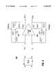
- FIG. 1shows one implementation of a semiconductor imaging device 100 having a programmable analog arithmetic circuit 120 that shares certain common electronic elements among different circuit modules.
- the imaging device 100includes a sensor array 110 for detecting an input scene, a row select logic 102 and a column select logic 104 for selecting pixels, and the arithmetic circuit 120 for performing certain arithmetic operations of pixel signals.
- the arithmetic circuit 120may include a block summing module that adds signals of a selected block of pixels, a block averaging module that produces an averaged signal for a selected block of pixels, an analog-to-digital converter and other arithmetic modules for operations such as addition, subtraction, multiplication, and division.
- a multiplexer 130is coupled to route the output signals from the arithmetic circuit 120 to proper output terminals, e.g., an analog output port 132, and a digital output port 134.
- a control circuit 140is also provided to control operations of the circuits 102, 104, 120, and 130.
- the control circuit 140is designed to control the electronic switches within the arithmetic circuit 120 so as to program it into different arithmetic circuit modules for different operations. The some switching schemes will be described in detail by examples.
- the sensor array 110may be any radiation-sensitive array of pixels capable of converting an input scene into pixel electrical signals.
- the preferred type of such sensor arraysis an active pixel sensor ("APS") where each pixel uses a CMOS image sensor 111 to directly convert photo-induced charge into an electrical signal and has an active transistor.
- Each pixelmay also include an in-pixel buffer circuit to buffer the signal and an in-pixel select transistor to output the buffered signal in response to a received control signal.
- U.S. Pat. No. 5,471,515 to Fossum et al.discloses a CMOS APS device capable of producing a reset signal (Vrst) of a pixel prior to an integration and a signal (Vsig) of that pixel at the end of the integration period.
- the reset signal Vrstrepresents non-photon-induced background level in the pixel and the signal Vsig includes both the reset signal and the photon-induced signal. Therefore, the difference between the reset signal Vrst and the signal Vsig is the photo-induced signal for that pixel and is free of KTC noise and fixed pattern noise.
- the signal acquisition in the imaging device 100preferably uses a column-parallel configuration.
- the arithmetic circuit 120is a linear array of arithmetic cells corresponding to columns of the sensor array 110. Each arithmetic cell receives signals from a respective column or more than one column, and is coupled with other arithmetic cells as desired.
- Each arithmetic cellin general includes multiple arithmetic modules that share certain common circuit elements. As an example, each arithmetic cell in the following description has three different arithmetic modules: a block summing module, a block averaging module, and an analog-to-digital converter.
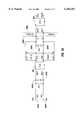
- FIG. 2shows one embodiment 200 of the arithmetic cell having a programmable analog arithmetic circuit ("PAAC") unit 210.
- the PAAC unit 210includes two switched capacitor integrators for summing and averaging pixel signals.
- Two inputs 202S and 202Rare coupled to receive the signals Vsig and Vrst from a respective column in the sensor array 110.
- the received signals Vsig and Vrstare processed to produce corresponding output signals at outputs 212S and 212R, respectively.
- Two sample and hold capacitors Csig 240S and Crst 240Rare respectively connected to the outputs 212S and 212R through two switches 220.
- a comparator 250is coupled to receive signals from the capacitors 240S and 240R for implementing a cyclic analog-to-digital converter.
- a reference voltage Vrefis coupled to the receiving ends of the capacitors 240S and 240R via switches 230.
- Inter-cell communication channelsare also provided to allow the PAAC unit in one cell to communicate with one or two adjacent PAAC units.
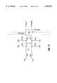
- FIG. 3shows a detailed circuit diagram of the PAAC unit 210.
- Two switched capacitor integrators 301 and 302, and capacitors C1, C2, C3, and C4are coupled through a network of switches to effect a block summing module and a block averaging module. They are further coupled to capacitors C5, C6, Csig, Crst and the comparator 250 to form a cyclic analog-to-digital converter.
- Switchable inter-cell communication channels 304a, 304b, 306a, 306b, 308a, and 308bconnect each arithmetic cell to two adjacent arithmetic cells and hence other arithmetic cells so that signals can be communicated between different columns.
- communication channels 304a and 304ballow charge sharing between the signal sampling capacitors 310S and between the reset sampling capacitors 310R of two adjacent cells, respectively.
- Communication channels 306a and 306ballow charge sharing between the signal sampling capacitors Cs1 and between the reset sampling capacitors Cs2 of the first switched capacitor integrators 301 of two adjacent cells, respectively.
- Each switched capacitor integratorincludes two integration channels: a signal channel for integrating a signal associated with the pixel signal Vsig and a reset channel for integrating a signal associated with the pixel reset Vrst.
- FIG. 4shows one embodiment of a switched capacitor integrator 400 based on an operational amplifier 401 where capacitors 410 (Cs1) and 420 (Cs2) respectively hold signals associated with Vsig and Vrst.
- This switched capacitor integrator 400can generate a differential output which is substantially free of any fixed pattern noise associated with a column. For example, one source of the column-wise fixed pattern noise is caused by the difference in the DC offsets of different operational amplifiers 401 in different columns.
- the integrator 400can operate in a way to compensate for the offset error at each step of integration and hence prevents such column-wise noise from accumulation in the integration process.
- FIG. 5Ashows an integration circuit based on the switched capacitor integrator 400 and illustrates how the column-wise noise is eliminated.
- the operation of the circuitis shown by the timing diagram in FIG. 5B.
- the integratoris reset with RSTC on, RSTCB is off to disconnect the feedback capacitors 410, 420 from the output of the amplifier 401.
- the pixel reset (Vrst) and signal (Vsig) levelsare sampled onto C1 and C2 respectively through PHIS and PHIR.
- RSTC1is also turned on so that the offset voltages are sampled onto C3 and C4 respectively.
- switches RSTC, RSTC1are turned off and RSTCB is turned on to terminate the reset process.
- the crowbar switch CBis closed so that the sampled signals on C1 and C2 are transferred to feedback capacitors C3 and C4.
- the output voltages on the signal side and the reset sideare
- Vcbis the potential at the shared node of C1 and C2 when switch CB is closed.
- the differential outputis given by,
- RSTC1is off all the time.
- the integratoris reset by turning off RSTCB and turning on RSTC.
- the integration chargeis stored on the feedback capacitors while resetting the integrator. Similar sampling of the new input levels Vrst,i and Vsig,i is performed as the integrator resets itself.
- the differential output voltage after ith step of integrationis,
- the op amp offsetis compensated at each step of integration. This compensation is achieved by sampling the errors onto the feedback capacitors during the first true reset period and onto the input capacitors during every reset period.
- this fully differential switched capacitor integratoralso rejects most of the switch feedthrough.
- the switch feedthroughwill appear as common mode voltage at the inputs and hence be rejected by the differential amplifier.
- the arithmetic cell 200can reconfigure itself to perform different arithmetic operations in response to control signals from the control circuit 140 by sharing the switched capacitor integrators 301 and 302 and other circuit elements among different arithmetic modules.
- the followingdescribes examples of controlling and reconfiguring the arithmetic cell 200 to function as a block averaging module, a block summing module, and a cyclic analog-to-digital converter.
- the PAAC unit 210can form a block averaging module by using the capacitors 310, 312, and the first switched capacitor integrator 301.
- FIG. 6Ashows the relevant part of the PAAC unit 210 that forms the block averaging module.
- the arithmetic circuit 120coupled to columns of the sensor array 110, becomes a bank of switched capacitor integrators as shown in FIG. 6A that are interconnected through a set of switches. By appropriately switching in additional capacitance from adjacent columns, switched capacitor charge integrators with variable integration gain can be achieved.
- a selected block of pixelsis averaged in two steps. First, image pixel values in a given row of the selected block are averaged. Second, averaged values of different rows in the selected block are averaged to produce the average value for the entire selected block. The block averaging is performed through charge sharing in this bank of capacitors with proper switching.
- FIG. 6Bis the timing diagram for operations of the switches in FIG. 6A to average a 3 ⁇ 3 block of pixels.
- the switch RDC1(1) for the first column of the selected blockis on and switches RDC1(2) and RDC1(3) for the second and third columns are off.
- the pixels of the first row in the selected blockare sampled into the capacitors C1 and C2 in the respective arithmetic cells when Switches 303S (SHS) and 303R (SHR) are on and the switch CB1 is off.
- the crowbar switch CB1is closed to transfer the averaged values of the first row for the signal side and the reset side onto capacitors Cs1 and Cs2 of the first switched capacitor integrator of the first column.
- the above averaging processrepeats to obtain the averaged values for the second and third rows in the selected block.
- the accumulated value in each of the capacitors Cs1 and Cs2 of the first columnis the sum of column averages for all three rows.
- This operationdistributes the accumulated charge in each of the capacitors Cs1 and Cs2 in the first column to the respective capacitors in the second and third columns. Therefore, the charge in each column is one third of the total charge previously stored in the first column and hence is the average value of the selected block.
- FIG. 6Cshows one circuit implementation of the block averaging module in FIG. 6A.
- the PAAC unit 210forms a block summing module by using the capacitors 310S, 310R, 320S, 320R and both the first and second switched capacitor integrators 301 and 302.
- FIG. 7Ashows the relevant part of the PAAC unit 210 that forms the block averaging module.
- the first switched capacitor integrator 301performs the row summing
- the second switched capacitor integrator 302performs the column summing.
- FIG. 7Cshows one circuit implementation of the block summing circuit in FIG. 7A.
- FIG. 7Bis the timing diagram for operations of the switches in FIG. 7A to sum the pixel signals from a 3 ⁇ 3 block.
- the block sumis performed in two steps. First, different rows in each column are sampled into the capacitors C1, C2 and then added in the capacitors Cs1, Cs2 in the first switched capacitor integrator. Since the switches LDC1 are on, the accumulated values in the capacitors Cs1 and Cs2 are transferred to the capacitors C3, and C4, respectively. This completes the row summing.
- the PAAC unit 210can also be reconfigured by proper switching to form a cyclic analog-to-digital converter using both switched capacitor integrators 301, 302 and the comparator 250.
- the cyclic configurationis preferred in this embodiment in order to share the circuit resources, such as the two switched capacitor integrators 301, 302, with the block averaging and block summing modules.
- the cyclic analog-to-digital conversionalso provides other advantages, including elimination of capacitor matching while still achieving a desired high conversion accuracy.
- FIG. 8shows a block diagram of a general fully differential cyclic analog-to-digital converter 800.
- the analog signal side and reset side loops of the ADC 800include sample switches SHS 810S and SHR 810R, a sample-and-hold (S/H) amplifier 820, a multiply-by-two (2 ⁇ ) amplifier 830, a comparator 840, a reference addition-subtraction circuit 850, and feedback switches 860S and 860R that respectively couple the signal side and reset side loops to respective inputs of the S/H amplifier 820.
- S/Hsample-and-hold
- 2 ⁇multiply-by-two
- the converter 800first samples input analog signals Vin+(Vsig) and Vin-(Vrst) to be converted onto the S/H amplifier.
- the multiply-by-two amplifier 830receives and amplifies the signals Vin+(Vsig) and Vin-(Vrst) to produce output signals Va+ and Va-.
- the signals Va+ and Va-are compared by the comparator 840 to extract digital information from the input signals Vin+ and Vin-. If Va+ is larger than Va-, the corresponding bit is set to 1. Accordingly, the reference Vref+ is subtracted from Va+ to produce a feedback signal Vb+ and the reference Vref- is then added to Va- to produce a feedback signal Vb-.
- Va-is larger than Va+
- the feedback signals Vb+ and Vb-are then fed back into the amplifier 820 by the feedback switches 860S and 860R for processing subsequent bits. This process repeats until the desired number of bits have been obtained.
- the digital data from the converter 800is a series of bits where the first bit is the most significant bit and last bit is the least significant bit.
- FIG. 9shows a cyclic ADC 900 formed from one configuration of the PAAC unit 210 and the comparator 250.
- the first switched capacitor integrator 301is configured as shown in FIG. 9A by proper switching to function as a sample-and-hold amplifier.
- the second switched capacitor integrator 302forms a multiply-by-two amplifier.
- FIG. 9Bshows the self-timing control logic for reference voltage subtraction and addition, which is integrated as part of each arithmetic cell.
- the cyclic ADC 900has a number of advantages. For example, the cyclic configuration allows the ADC 900 to share the integrators 301 and 302 that are used to perform arithmetic operations. In addition, the differential operation mode of the signal side and the reset side automatically eliminates any common-mode offset, e.g., fixed pattern noise, from the digital output of the comparator 840.
- the operation of the cyclic ADC 900is illustrated in the timing diagram in FIG. 10 for 8-bit analog-to-digital conversion.
- the differential signalis introduced through the selection switches SHS and SHR and is sampled onto the S/H amplifier. While this voltage value is held, it is multiplied by two by the switched capacitor amplifier 302 using ratio-independent algorithm disclosed in Li et al., supra. This multiplication is achieved in two steps.
- the output signals on both the signal side and the reset side of the integrator 302are (C3/Cs1)Vsig(C3) and (C4/Cs2)Vrst(C4), respectively, which depend on capacitor ratios (C3/Cs1) and (C4/Cs2).
- RSTCBis turned off and RSTC1 and TRANSFER are on in order to exchange the positions of the integrating capacitor and the sampling capacitor on both signal side and the reset side.
- Two complementary reference voltage Vref+ and Vref-are provided to the signal side and reset side loops through capacitors 330S (C5) and 330R (C6), respectively.
- the capacitors C5 and C6allow both the subtraction and addition of the reference voltages.
- the switch labeled FEEDBACKfeeds the signal back into the loop. This converter takes six clock cycles to complete a 1-bit conversion. Hence, the total conversion time for 8-bit conversion is 48 clock cycles.
- FIG. 9Cshows one circuit implementation of the ACD in FIG. 9.
- the above arithmetic circuit 120can be configured by proper switching to perform addition, subtraction, multiplication, and division as general arithmetic operations. Hence, any other operations based on the above general arithmetic operations can be performed.
- the PAAC unit 210can be configured into a switched capacitor integrator shown in FIG. 5A to carry out basic addition operations.
- the PAAC unit 210can also be switched into the configuration of FIG. 7A to perform additions.
- the switches ADD in the PAAC unit 210can be used to add and the switches SUB can be used to subtract.
- Multiplicationmay be implemented as two or more additions.
- FIG. 11shows one configuration of the PAAC unit 210 for performing a division by 3.
- Three arithmetic cellsare needed to perform the division.
- the pixel signal and reset valuesare respectively sampled into the sampling capacitors C1 and C2 when switches SHS and SHR are on and the switch CB1 is off.
- the sampled values for signal side and the reset sideare transferred onto capacitor Cs1 and Cs2 of the integrator 301 of the first column by turning on switch CB1 and switch RDC1(1) of first column.
- This operationdistributes the accumulated charge in each of the capacitors Cs1 and Cs2 in the first column and the respective capacitors in the second and third columns which is one third of the pixel value.
- the FEEDBACK switchcan be used to feed back any value at any time as needed.
- the arithmetic circuit 120can be used to perform a wide range of operations without additional circuit elements.
- Such versatile resource-sharing circuitcan be integrated on an imaging sensor chip for many imaging processing applications.
- the on-chip column parallel cyclic ADCprovides flexibility of a digital interface and greatly enhances system robustness through noise immunity. This is in part because the digital output is immune from electromagnetic pickup and crosstalk.
- integration of the ADC on the sensor chipalso simplifies the overall system design.
- the arithmetic circuit 120can provide programmable multiresolution capabilities to the imaging device 100 in FIG. 1.
- the block averagingcan be used to produce images of variable resolutions for machine vision algorithms such as stereo vision range finding.
- the resolutioncan be adjusted according to the lighting conditions and the field of view of the target object. This functionality can enhance the speed performance of those algorithms and provide the flexibility in selecting a desired image size.
- the block summingcan be used to sum pixel signals of pixel blocks in different sizes when desired in order to increase the effective dynamic range of the device. Therefore, the block averaging and the block summing of the arithmetic circuit 120 provides a light-adaptive sensing mechanism in the imaging device 100 (e.g., the light adaptable machine vision algorithm). This feature is especially desirable in imaging applications under variable lighting conditions.
- the above arithmetic circuit 120also inherently has image signal compression property.
- the chip using PAACcould be used in a pyramid coding scheme useful for image compression and progressive transmission.
- the PAACcould be used to find its way into 3-D recognition and stereo image compression systems, enhancing performance by facilitating some processing tasks such as finding correspondence, reducing block matching operation with block averaging.
- the arithmetic circuit 120may also be used for basic image processing operations such as generating the binary image with multiple threshold because of PAAC subtraction capability, simple edge detection, etc. Such features are useful in pattern recognition area and machine vision systems. Furthermore, on-chip motion detection capability based on the difference between two image frames can also be implemented in the arithmetic circuit 120. This feature is essential to a system that tracks moving targets.
- the above and other signal processing capabilitiescan be integrated on the imaging sensor chip because of the resource sharing architecture of the arithmetic circuit 120.
- resource sharingallows implementation of multiple arithmetic circuit modules in a remarkably reduced silicon area and makes such implementation commercially viable.
- the above circuitsuse two parallel signal paths, one for signals associated with Vsig and another for signals associated with Vrst, in order to take advantage of the two outputs from the APS image sensor for reducing noise.
- the above circuitscan be operated with only one of the two signal paths or may be constructed to have only one signal path.
- the number and the manner of the communication channels between different columnsmay be changed to meet the specific needs of an application.
- the deployment of the electronic switches and associated switching schemesmay be also be modified based on the embodiments disclosed herein.
Landscapes
- Engineering & Computer Science (AREA)
- Multimedia (AREA)
- Signal Processing (AREA)
- Transforming Light Signals Into Electric Signals (AREA)
Abstract
Description
Vos=-(C1/C3) (Vsig-Vcb),
Vor=-(C2/C4) (Vrst-Vcb),
Vor-Vos=-(C2/C4)Vrst+(C1/C3)Vsig=-(C1/C3) (Vrst-Vsig),
Vor,i-Vos,i=Vor,i-1-Vos,i-1-(C1/C3) (Vrst,i-Vsig,i).
TABLE 1 ______________________________________ Vin+ Vin- Va+ Va- Vb+ Vb- Output ______________________________________ 0.8 -0.8 1.6 -1.6 0.6 -0.6 1 1.2 -1.2 0.2 -0.2 1 0.4 -0.4 -0.6 0.6 0 -1.2 1.2 -0.2 0.2 0 -0.4 0.4 0.6 -0.6 1 ______________________________________
Claims (23)
Priority Applications (1)
| Application Number | Priority Date | Filing Date | Title |
|---|---|---|---|
| US09/277,617US6166367A (en) | 1998-03-26 | 1999-03-26 | Programmable analog arithmetic circuit for imaging sensor |
Applications Claiming Priority (2)
| Application Number | Priority Date | Filing Date | Title |
|---|---|---|---|
| US7971298P | 1998-03-26 | 1998-03-26 | |
| US09/277,617US6166367A (en) | 1998-03-26 | 1999-03-26 | Programmable analog arithmetic circuit for imaging sensor |
Publications (1)
| Publication Number | Publication Date |
|---|---|
| US6166367Atrue US6166367A (en) | 2000-12-26 |
Family
ID=26762349
Family Applications (1)
| Application Number | Title | Priority Date | Filing Date |
|---|---|---|---|
| US09/277,617Expired - LifetimeUS6166367A (en) | 1998-03-26 | 1999-03-26 | Programmable analog arithmetic circuit for imaging sensor |
Country Status (1)
| Country | Link |
|---|---|
| US (1) | US6166367A (en) |
Cited By (130)
| Publication number | Priority date | Publication date | Assignee | Title |
|---|---|---|---|---|
| US6441766B1 (en)* | 2000-11-22 | 2002-08-27 | Sunplus Technology Co., Ltd. | Charge integration algorithmic analog-to-digital converter and its converting method |
| US6452149B1 (en)* | 2000-03-07 | 2002-09-17 | Kabushiki Kaisha Toshiba | Image input system including solid image sensing section and signal processing section |
| US20020154232A1 (en)* | 2000-05-19 | 2002-10-24 | Tull Damon L. | Preventing blur caused by motion of the subject in a digital image |
| US20020158982A1 (en)* | 2001-04-26 | 2002-10-31 | Fujitsu Limited | X-Y address type solid-state image pickup device |
| US20030011694A1 (en)* | 2001-07-16 | 2003-01-16 | Bart Dierickx | Method to adjust the signal level of an active pixel and corresponding active pixel |
| US6515271B1 (en)* | 1999-05-21 | 2003-02-04 | Olympus Optical Co., Ltd. | CMOS image sensor unit with serial transmitting function |
| US20030043064A1 (en)* | 2001-08-31 | 2003-03-06 | Fuji Photo Film Co., Ltd | Signal detecting method and signal detecting device |
| US6535152B2 (en) | 2000-12-30 | 2003-03-18 | Hynix Semiconductor Inc. | Analog-to-digital converter having gamma-corrected reference voltages |
| US6587145B1 (en)* | 1998-08-20 | 2003-07-01 | Syscan Technology (Shenzhen) Co., Ltd. | Image sensors generating digital signals from light integration processes |
| US6614320B1 (en) | 2000-10-26 | 2003-09-02 | Cypress Semiconductor Corporation | System and method of providing a programmable clock architecture for an advanced microcontroller |
| US20030201379A1 (en)* | 2000-11-27 | 2003-10-30 | Moshe Stark | Noise floor reduction in image sensors |
| WO2002098112A3 (en)* | 2001-05-29 | 2003-11-20 | Transchip Inc | Patent application cmos imager for cellular applications and methods of using such |
| US20040012676A1 (en)* | 2002-03-15 | 2004-01-22 | Affymetrix, Inc., A Corporation Organized Under The Laws Of Delaware | System, method, and product for scanning of biological materials |
| US20040012697A1 (en)* | 2002-07-18 | 2004-01-22 | Giuseppe Rossi | Varying capacitance that receives signals from sensing elements |
| US6693670B1 (en)* | 1999-07-29 | 2004-02-17 | Vision - Sciences, Inc. | Multi-photodetector unit cell |
| US20040036453A1 (en)* | 2002-08-23 | 2004-02-26 | Giuseppe Rossi | Fully differential reference driver for pipeline analog to digital converter |
| US20040036797A1 (en)* | 2000-07-05 | 2004-02-26 | Moshe Stark | Dynamic range compression method |
| US20040081793A1 (en)* | 2001-04-17 | 2004-04-29 | Byrne David Vincent | Trench cover |
| US6741198B2 (en) | 2001-06-20 | 2004-05-25 | R3 Logic, Inc. | High resolution, low power, wide dynamic range imager with embedded pixel processor and DRAM storage |
| US6757019B1 (en)* | 1999-03-13 | 2004-06-29 | The Board Of Trustees Of The Leland Stanford Junior University | Low-power parallel processor and imager having peripheral control circuitry |
| US20040172490A1 (en)* | 2001-04-11 | 2004-09-02 | Mark Stadler | Reduced-overhead dma |
| US6801258B1 (en)* | 1998-03-16 | 2004-10-05 | California Institute Of Technology | CMOS integration sensor with fully differential column readout circuit for light adaptive imaging |
| US20040207739A1 (en)* | 2003-04-21 | 2004-10-21 | Giuseppe Rossi | Multi path power for CMOS imagers |
| US20040222351A1 (en)* | 2003-05-07 | 2004-11-11 | Giuseppe Rossi | Multiple crawbar switching in charge domain linear operations |
| EP1478171A1 (en)* | 2003-05-12 | 2004-11-17 | Istituto Trentino Di Cultura | A light-sensitive pixel and an integrated vision sensor comprising a plurality of shuch pixels |
| US20040233324A1 (en)* | 2001-05-29 | 2004-11-25 | Transchip, Inc. | Systems and methods for power conservation in a CMOS imager |
| US6829190B1 (en) | 2002-06-13 | 2004-12-07 | Cypress Semiconductor Corporation | Method and system for programming a memory device |
| US6839452B1 (en)* | 1999-11-23 | 2005-01-04 | California Institute Of Technology | Dynamically re-configurable CMOS imagers for an active vision system |
| US6859884B1 (en) | 2000-10-26 | 2005-02-22 | Cypress Semiconductor Corporation | Method and circuit for allowing a microprocessor to change its operating frequency on-the-fly |
| US20050059062A1 (en)* | 2003-08-08 | 2005-03-17 | Affymetrix, Inc. | System, method, and product for scanning of biological materials employing dual analog integrators |
| US6873363B1 (en)* | 1999-02-16 | 2005-03-29 | Micron Technology Inc. | Technique for flagging oversaturated pixels |
| US6873282B1 (en)* | 2004-03-04 | 2005-03-29 | Charles Douglas Murphy | Differential time-to-threshold A/D conversion in digital imaging arrays |
| US20050073451A1 (en)* | 2003-07-14 | 2005-04-07 | University Of Rochester | Multiplexed-input-separated sigma-delta analog-to-digital converter design for pixel-level analog-to-digital conversion |
| US6888568B1 (en)* | 1999-08-19 | 2005-05-03 | Dialog Semiconductor Gmbh | Method and apparatus for controlling pixel sensor elements |
| US6910126B1 (en) | 2000-10-26 | 2005-06-21 | Cypress Microsystems, Inc. | Programming methodology and architecture for a programmable analog system |
| US6950954B1 (en) | 2000-10-26 | 2005-09-27 | Cypress Semiconductor Corporation | Method and circuit for synchronizing a write operation between an on-chip microprocessor and an on-chip programmable analog device operating at different frequencies |
| US6965395B1 (en) | 2000-09-12 | 2005-11-15 | Dialog Semiconductor Gmbh | Methods and systems for detecting defective imaging pixels and pixel values |
| US6967511B1 (en)* | 2000-10-26 | 2005-11-22 | Cypress Semiconductor Corporation | Method for synchronizing and resetting clock signals supplied to multiple programmable analog blocks |
| US20050270394A1 (en)* | 2004-05-25 | 2005-12-08 | Bart Dierickx | Method and pixel for performing correlated double sampling |
| US20060008236A1 (en)* | 2001-04-27 | 2006-01-12 | Sam Leeman | Optical fibre sealing |
| US7002628B1 (en)* | 1998-03-31 | 2006-02-21 | Micron Technology, Inc. | Analog to digital converter with internal data storage |
| US20060044907A1 (en)* | 2004-09-01 | 2006-03-02 | Leonard Forbes | Sample and hold memory sense amplifier |
| US20060044903A1 (en)* | 2004-08-31 | 2006-03-02 | Micron Technology, Inc. | Switched capacitor DRAM sense amplifier with immunity to mismatch and offsets |
| US20060044012A1 (en)* | 2004-08-31 | 2006-03-02 | Micron Technology, Inc. | Capacitively-coupled level restore circuits for low voltage swing logic circuits |
| US20060055577A1 (en)* | 2004-08-31 | 2006-03-16 | Christian Boemler | Minimized differential SAR-type column-wide ADC for CMOS image sensors |
| US7023257B1 (en) | 2000-10-26 | 2006-04-04 | Cypress Semiconductor Corp. | Architecture for synchronizing and resetting clock signals supplied to multiple programmable analog blocks |
| US20060081766A1 (en)* | 2000-07-27 | 2006-04-20 | Canon Kabushiki Kaisha | Image sensing apparatus |
| US20060108506A1 (en)* | 2004-11-23 | 2006-05-25 | Dialog Semiconductor Gmbh | Column averaging/row binning circuit for image sensor resolution adjustment in lower intensity light environment |
| US20060113459A1 (en)* | 2004-11-23 | 2006-06-01 | Dialog Semiconductor Gmbh | Image sensor having resolution adjustment employing an analog column averaging/row averaging for high intensity light or row binning for low intensity light |
| US20060113458A1 (en)* | 2004-11-30 | 2006-06-01 | Dialog Semiconductor Gmbh | Column averaging/row averaging circuit for image sensor resolution adjustment in high intensity light environment |
| US20060135107A1 (en)* | 2001-10-26 | 2006-06-22 | Staszewski Robert B | Removing close-in interferers through a feedback loop |
| US20060187328A1 (en)* | 2005-02-23 | 2006-08-24 | Samsung Electronics Co.,Ltd. | Solid state image sensing device for analog-averaging and sub-sampling of image signals at a variable sub-sampling rate and method of driving the same |
| US20060232676A1 (en)* | 2005-04-15 | 2006-10-19 | Micron Technology, Inc. | Column-parallel sigma-delta analog-to-digital conversion for imagers |
| US7133073B1 (en) | 1999-08-19 | 2006-11-07 | Dialog Imaging Systems Gmbh | Method and apparatus for color interpolation |
| US20070030262A1 (en)* | 2005-08-03 | 2007-02-08 | Takanobu Ambo | Semiconductor integrated circuit device |
| US20070090986A1 (en)* | 2005-10-21 | 2007-04-26 | Shigeyuki Komatsu | Analog-digital converter |
| US20070187794A1 (en)* | 2005-06-17 | 2007-08-16 | Toppan Printing Co., Ltd. | Imaging device |
| US20070216564A1 (en)* | 2006-03-14 | 2007-09-20 | Sony Corporation | AD converter device, physical quantity distribution detecting unit and imaging apparatus |
| US20070263127A1 (en)* | 2006-03-07 | 2007-11-15 | Transchip, Inc. | Low Noise Gamma Function In Digital Image Capture Systems And Methods |
| WO2007135153A1 (en)* | 2006-05-23 | 2007-11-29 | Thomson Licensing | Image sensor circuit |
| US20080074521A1 (en)* | 2006-08-30 | 2008-03-27 | Alf Olsen | Amplifier offset cancellation devices, systems, and methods |
| WO2008108884A1 (en) | 2007-03-08 | 2008-09-12 | Imagerlabs, Inc. | Ultra low noise cmos imager |
| US20080234475A1 (en)* | 2007-03-19 | 2008-09-25 | Vasulinga Ravikumar | Process for the synthesis of 2'-o-substituted purines |
| US20090015692A1 (en)* | 2007-07-13 | 2009-01-15 | Micron Technology, Inc. | Methods, systems, and devices for offset compensation in cmos imagers |
| WO2009046421A1 (en)* | 2007-10-04 | 2009-04-09 | Centeye, Inc. | Feature detecting vision sensor |
| US20090230289A1 (en)* | 2006-11-29 | 2009-09-17 | Cypress Semiconductor Corporation | Pixel Structure Having Shielded Storage Node |
| US20090303358A1 (en)* | 2006-07-31 | 2009-12-10 | Shoji Kawahito | A/d converter and readout circuit |
| US20090322577A1 (en)* | 2008-06-25 | 2009-12-31 | Robert Johansson | Low-power column parallel cyclic analog-to-digital converter |
| US20100072350A1 (en)* | 2008-09-22 | 2010-03-25 | Cypress Semiconductor Corporation | Active pixel with precharging circuit |
| US20100079632A1 (en)* | 2008-09-26 | 2010-04-01 | Tom Walschap | Correlated double sampling pixel |
| US7737724B2 (en) | 2007-04-17 | 2010-06-15 | Cypress Semiconductor Corporation | Universal digital block interconnection and channel routing |
| US7750958B1 (en) | 2005-03-28 | 2010-07-06 | Cypress Semiconductor Corporation | Pixel structure |
| US7761845B1 (en) | 2002-09-09 | 2010-07-20 | Cypress Semiconductor Corporation | Method for parameterizing a user module |
| US7765095B1 (en) | 2000-10-26 | 2010-07-27 | Cypress Semiconductor Corporation | Conditional branching in an in-circuit emulation system |
| US7770113B1 (en) | 2001-11-19 | 2010-08-03 | Cypress Semiconductor Corporation | System and method for dynamically generating a configuration datasheet |
| US7774190B1 (en) | 2001-11-19 | 2010-08-10 | Cypress Semiconductor Corporation | Sleep and stall in an in-circuit emulation system |
| US7808022B1 (en) | 2005-03-28 | 2010-10-05 | Cypress Semiconductor Corporation | Cross talk reduction |
| US7825688B1 (en) | 2000-10-26 | 2010-11-02 | Cypress Semiconductor Corporation | Programmable microcontroller architecture(mixed analog/digital) |
| US7844437B1 (en) | 2001-11-19 | 2010-11-30 | Cypress Semiconductor Corporation | System and method for performing next placements and pruning of disallowed placements for programming an integrated circuit |
| US7868928B2 (en) | 2006-03-15 | 2011-01-11 | Samsung Electronics Co., Ltd. | Low noise color correction matrix function in digital image capture systems and methods |
| US7893724B2 (en) | 2004-03-25 | 2011-02-22 | Cypress Semiconductor Corporation | Method and circuit for rapid alignment of signals |
| US20110228122A1 (en)* | 2010-03-17 | 2011-09-22 | Canon Kabushiki Kaisha | Image pickup device and image pickup system |
| US8026739B2 (en) | 2007-04-17 | 2011-09-27 | Cypress Semiconductor Corporation | System level interconnect with programmable switching |
| US8042093B1 (en) | 2001-11-15 | 2011-10-18 | Cypress Semiconductor Corporation | System providing automatic source code generation for personalization and parameterization of user modules |
| US8045028B1 (en) | 2007-04-23 | 2011-10-25 | On Semiconductor Trading Ltd. | Six transistor (6T) pixel architecture |
| US8049569B1 (en) | 2007-09-05 | 2011-11-01 | Cypress Semiconductor Corporation | Circuit and method for improving the accuracy of a crystal-less oscillator having dual-frequency modes |
| US20110283057A1 (en)* | 2000-10-26 | 2011-11-17 | Cypress Semiconductor Corporation | Microcontroller Programmable System on a Chip |
| US8069436B2 (en) | 2004-08-13 | 2011-11-29 | Cypress Semiconductor Corporation | Providing hardware independence to automate code generation of processing device firmware |
| US8069428B1 (en) | 2001-10-24 | 2011-11-29 | Cypress Semiconductor Corporation | Techniques for generating microcontroller configuration information |
| US8069405B1 (en) | 2001-11-19 | 2011-11-29 | Cypress Semiconductor Corporation | User interface for efficiently browsing an electronic document using data-driven tabs |
| US8067948B2 (en) | 2006-03-27 | 2011-11-29 | Cypress Semiconductor Corporation | Input/output multiplexer bus |
| US8078894B1 (en) | 2007-04-25 | 2011-12-13 | Cypress Semiconductor Corporation | Power management architecture, method and configuration system |
| US8078970B1 (en) | 2001-11-09 | 2011-12-13 | Cypress Semiconductor Corporation | Graphical user interface with user-selectable list-box |
| US8082531B2 (en) | 2004-08-13 | 2011-12-20 | Cypress Semiconductor Corporation | Method and an apparatus to design a processing system using a graphical user interface |
| US8085100B2 (en) | 2005-02-04 | 2011-12-27 | Cypress Semiconductor Corporation | Poly-phase frequency synthesis oscillator |
| US8085067B1 (en) | 2005-12-21 | 2011-12-27 | Cypress Semiconductor Corporation | Differential-to-single ended signal converter circuit and method |
| US8089461B2 (en) | 2005-06-23 | 2012-01-03 | Cypress Semiconductor Corporation | Touch wake for electronic devices |
| US8092083B2 (en) | 2007-04-17 | 2012-01-10 | Cypress Semiconductor Corporation | Temperature sensor with digital bandgap |
| US8103497B1 (en) | 2002-03-28 | 2012-01-24 | Cypress Semiconductor Corporation | External interface for event architecture |
| US8103496B1 (en) | 2000-10-26 | 2012-01-24 | Cypress Semicondutor Corporation | Breakpoint control in an in-circuit emulation system |
| US8120408B1 (en) | 2005-05-05 | 2012-02-21 | Cypress Semiconductor Corporation | Voltage controlled oscillator delay cell and method |
| US8130025B2 (en) | 2007-04-17 | 2012-03-06 | Cypress Semiconductor Corporation | Numerical band gap |
| US8149048B1 (en) | 2000-10-26 | 2012-04-03 | Cypress Semiconductor Corporation | Apparatus and method for programmable power management in a programmable analog circuit block |
| US8160864B1 (en) | 2000-10-26 | 2012-04-17 | Cypress Semiconductor Corporation | In-circuit emulator and pod synchronized boot |
| US8233735B2 (en) | 1994-02-10 | 2012-07-31 | Affymetrix, Inc. | Methods and apparatus for detection of fluorescently labeled materials |
| US8286125B2 (en) | 2004-08-13 | 2012-10-09 | Cypress Semiconductor Corporation | Model for a hardware device-independent method of defining embedded firmware for programmable systems |
| US8310577B1 (en) | 1999-08-19 | 2012-11-13 | Youliza, Gehts B.V. Limited Liability Company | Method and apparatus for color compensation |
| US8402313B1 (en) | 2002-05-01 | 2013-03-19 | Cypress Semiconductor Corporation | Reconfigurable testing system and method |
| US8416117B2 (en)* | 2011-08-11 | 2013-04-09 | Atmel Corporation | Analog to digital converter with dual integrating capacitor systems |
| US8421666B2 (en)* | 2011-08-11 | 2013-04-16 | Atmel Corporation | Analog to digital converter with adjustable conversion window |
| US8499270B1 (en) | 2007-04-25 | 2013-07-30 | Cypress Semiconductor Corporation | Configuration of programmable IC design elements |
| US8516025B2 (en) | 2007-04-17 | 2013-08-20 | Cypress Semiconductor Corporation | Clock driven dynamic datapath chaining |
| US8533677B1 (en) | 2001-11-19 | 2013-09-10 | Cypress Semiconductor Corporation | Graphical user interface for dynamically reconfiguring a programmable device |
| US20140056089A1 (en)* | 2011-05-12 | 2014-02-27 | Micron Technology, Inc. | Sense amplifiers, memories, and apparatuses and methods for sensing a data state of a memory cell |
| US20150222825A1 (en)* | 2014-02-04 | 2015-08-06 | Semiconductor Components Industries, Llc | Arithmetic memory with horizontal binning capabilities for imaging systems |
| US9343489B2 (en) | 2011-05-12 | 2016-05-17 | DePuy Synthes Products, Inc. | Image sensor for endoscopic use |
| US9448964B2 (en) | 2009-05-04 | 2016-09-20 | Cypress Semiconductor Corporation | Autonomous control in a programmable system |
| US9462234B2 (en) | 2012-07-26 | 2016-10-04 | DePuy Synthes Products, Inc. | Camera system with minimal area monolithic CMOS image sensor |
| CN106133476A (en)* | 2014-03-05 | 2016-11-16 | 西克Ivp股份公司 | For providing the view data of 3D feature about object and the image sensing apparatus of information and the system of measurement |
| US20160345862A1 (en)* | 2015-06-01 | 2016-12-01 | Pixart Imaging Inc. | Optical respiration rate detection device and detection method thereof |
| US9564902B2 (en) | 2007-04-17 | 2017-02-07 | Cypress Semiconductor Corporation | Dynamically configurable and re-configurable data path |
| US9720805B1 (en) | 2007-04-25 | 2017-08-01 | Cypress Semiconductor Corporation | System and method for controlling a target device |
| US9767342B2 (en) | 2009-05-22 | 2017-09-19 | Affymetrix, Inc. | Methods and devices for reading microarrays |
| EP3261256A1 (en)* | 2016-06-23 | 2017-12-27 | Nxp B.V. | Sensor apparatuses and methods |
| US10206561B2 (en) | 2013-02-28 | 2019-02-19 | DePuy Synthes Products, Inc. | Videostroboscopy of vocal cords with CMOS sensors |
| US10517469B2 (en) | 2013-03-15 | 2019-12-31 | DePuy Synthes Products, Inc. | Image sensor synchronization without input clock and data transmission clock |
| US10750933B2 (en) | 2013-03-15 | 2020-08-25 | DePuy Synthes Products, Inc. | Minimize image sensor I/O and conductor counts in endoscope applications |
| US10827090B1 (en)* | 2019-09-16 | 2020-11-03 | Innolux Corporation | Electronic device and method for operating electronic device |
| US20220231695A1 (en)* | 2021-01-15 | 2022-07-21 | Senbiosys | Cyclic adc with voting and adaptive averaging |
| US11771375B2 (en) | 2014-09-26 | 2023-10-03 | Pixart Imaging Inc. | Respiration rate detection device and breath detection device adopting motion denoising |
Citations (14)
| Publication number | Priority date | Publication date | Assignee | Title |
|---|---|---|---|---|
| US5097305A (en)* | 1991-02-19 | 1992-03-17 | Synaptics Corporation | Integrating photosensor and imaging system having wide dynamic range |
| US5324958A (en)* | 1991-02-19 | 1994-06-28 | Synaptics, Incorporated | Integrating imaging systgem having wide dynamic range with sample/hold circuits |
| US5410348A (en)* | 1992-02-14 | 1995-04-25 | Sony Corporation | Amplifier type image sensor with shutter operation |
| US5436442A (en)* | 1992-11-20 | 1995-07-25 | General Electric Company | High temperature photodetector array |
| US5512750A (en)* | 1994-06-03 | 1996-04-30 | Martin Marietta Corporation | A-dual band IR sensor having two monolithically integrated staring detector arrays for simultaneous, coincident image readout |
| US5793322A (en)* | 1995-11-07 | 1998-08-11 | California Institute Of Technology | Successive approximation analog-to-digital converter using balanced charge integrating amplifiers |
| US5841126A (en)* | 1994-01-28 | 1998-11-24 | California Institute Of Technology | CMOS active pixel sensor type imaging system on a chip |
| US5886659A (en)* | 1996-08-21 | 1999-03-23 | California Institute Of Technology | On-focal-plane analog-to-digital conversion for current-mode imaging devices |
| WO1999046929A1 (en)* | 1998-03-10 | 1999-09-16 | Photobit Corporation | Charge-domain analog readout for an image sensor |
| US6005619A (en)* | 1997-10-06 | 1999-12-21 | Photobit Corporation | Quantum efficiency improvements in active pixel sensors |
| US6021172A (en)* | 1994-01-28 | 2000-02-01 | California Institute Of Technology | Active pixel sensor having intra-pixel charge transfer with analog-to-digital converter |
| US6043690A (en)* | 1998-03-10 | 2000-03-28 | Photobit Corporation | Bidirectional follower for driving a capacitive load |
| US6049247A (en)* | 1997-12-16 | 2000-04-11 | Photobit Corporation | Low-voltage common source switched-capacitor amplifier |
| US6087970A (en)* | 1998-03-11 | 2000-07-11 | Photobit Corporation | Analog-to-digital conversion |
- 1999
- 1999-03-26USUS09/277,617patent/US6166367A/ennot_activeExpired - Lifetime
Patent Citations (14)
| Publication number | Priority date | Publication date | Assignee | Title |
|---|---|---|---|---|
| US5097305A (en)* | 1991-02-19 | 1992-03-17 | Synaptics Corporation | Integrating photosensor and imaging system having wide dynamic range |
| US5324958A (en)* | 1991-02-19 | 1994-06-28 | Synaptics, Incorporated | Integrating imaging systgem having wide dynamic range with sample/hold circuits |
| US5410348A (en)* | 1992-02-14 | 1995-04-25 | Sony Corporation | Amplifier type image sensor with shutter operation |
| US5436442A (en)* | 1992-11-20 | 1995-07-25 | General Electric Company | High temperature photodetector array |
| US5841126A (en)* | 1994-01-28 | 1998-11-24 | California Institute Of Technology | CMOS active pixel sensor type imaging system on a chip |
| US6021172A (en)* | 1994-01-28 | 2000-02-01 | California Institute Of Technology | Active pixel sensor having intra-pixel charge transfer with analog-to-digital converter |
| US5512750A (en)* | 1994-06-03 | 1996-04-30 | Martin Marietta Corporation | A-dual band IR sensor having two monolithically integrated staring detector arrays for simultaneous, coincident image readout |
| US5793322A (en)* | 1995-11-07 | 1998-08-11 | California Institute Of Technology | Successive approximation analog-to-digital converter using balanced charge integrating amplifiers |
| US5886659A (en)* | 1996-08-21 | 1999-03-23 | California Institute Of Technology | On-focal-plane analog-to-digital conversion for current-mode imaging devices |
| US6005619A (en)* | 1997-10-06 | 1999-12-21 | Photobit Corporation | Quantum efficiency improvements in active pixel sensors |
| US6049247A (en)* | 1997-12-16 | 2000-04-11 | Photobit Corporation | Low-voltage common source switched-capacitor amplifier |
| WO1999046929A1 (en)* | 1998-03-10 | 1999-09-16 | Photobit Corporation | Charge-domain analog readout for an image sensor |
| US6043690A (en)* | 1998-03-10 | 2000-03-28 | Photobit Corporation | Bidirectional follower for driving a capacitive load |
| US6087970A (en)* | 1998-03-11 | 2000-07-11 | Photobit Corporation | Analog-to-digital conversion |
Cited By (266)
| Publication number | Priority date | Publication date | Assignee | Title |
|---|---|---|---|---|
| US8233735B2 (en) | 1994-02-10 | 2012-07-31 | Affymetrix, Inc. | Methods and apparatus for detection of fluorescently labeled materials |
| US6801258B1 (en)* | 1998-03-16 | 2004-10-05 | California Institute Of Technology | CMOS integration sensor with fully differential column readout circuit for light adaptive imaging |
| US7002628B1 (en)* | 1998-03-31 | 2006-02-21 | Micron Technology, Inc. | Analog to digital converter with internal data storage |
| US6587145B1 (en)* | 1998-08-20 | 2003-07-01 | Syscan Technology (Shenzhen) Co., Ltd. | Image sensors generating digital signals from light integration processes |
| US6873363B1 (en)* | 1999-02-16 | 2005-03-29 | Micron Technology Inc. | Technique for flagging oversaturated pixels |
| US20050128329A1 (en)* | 1999-02-16 | 2005-06-16 | Micron Technology, Inc. | Technique for flagging oversaturated pixels |
| US8031260B2 (en) | 1999-02-16 | 2011-10-04 | Aptina Imaging Corporation | Technique for flagging oversaturated pixels |
| US6757019B1 (en)* | 1999-03-13 | 2004-06-29 | The Board Of Trustees Of The Leland Stanford Junior University | Low-power parallel processor and imager having peripheral control circuitry |
| US6515271B1 (en)* | 1999-05-21 | 2003-02-04 | Olympus Optical Co., Ltd. | CMOS image sensor unit with serial transmitting function |
| US20040169752A1 (en)* | 1999-07-29 | 2004-09-02 | Moshe Stark | Multi-photodetector unit cell |
| US6693670B1 (en)* | 1999-07-29 | 2004-02-17 | Vision - Sciences, Inc. | Multi-photodetector unit cell |
| US7623163B2 (en) | 1999-08-19 | 2009-11-24 | Digital Imaging Systems Gmbh | Method and apparatus for color interpolation |
| US20070052813A1 (en)* | 1999-08-19 | 2007-03-08 | Sarit Neter | Method and apparatus for color interpolation |
| US20050185075A1 (en)* | 1999-08-19 | 2005-08-25 | Dialog Semiconductor Gmbh | Method and apparatus for controlling pixel sensor elements |
| US8310577B1 (en) | 1999-08-19 | 2012-11-13 | Youliza, Gehts B.V. Limited Liability Company | Method and apparatus for color compensation |
| US6888568B1 (en)* | 1999-08-19 | 2005-05-03 | Dialog Semiconductor Gmbh | Method and apparatus for controlling pixel sensor elements |
| US8164665B2 (en) | 1999-08-19 | 2012-04-24 | Youliza, Gehts B.V. Limited Liability Company | Method and apparatus for controlling pixel sensor elements |
| US7133073B1 (en) | 1999-08-19 | 2006-11-07 | Dialog Imaging Systems Gmbh | Method and apparatus for color interpolation |
| US6839452B1 (en)* | 1999-11-23 | 2005-01-04 | California Institute Of Technology | Dynamically re-configurable CMOS imagers for an active vision system |
| US6928535B2 (en) | 2000-03-07 | 2005-08-09 | Kabushiki Kaisha Toshiba | Data input/output configuration for transfer among processing elements of different processors |
| US20020195544A1 (en)* | 2000-03-07 | 2002-12-26 | Kabushiki Kaisha Toshiba | Image input system including solid image sensing section and signal processing section |
| US6452149B1 (en)* | 2000-03-07 | 2002-09-17 | Kabushiki Kaisha Toshiba | Image input system including solid image sensing section and signal processing section |
| US20020154232A1 (en)* | 2000-05-19 | 2002-10-24 | Tull Damon L. | Preventing blur caused by motion of the subject in a digital image |
| US7050091B2 (en)* | 2000-05-19 | 2006-05-23 | Tull Damon L | Method for preventing blurring of a digital image by monitoring a rate of change of photon reception |
| US20040036797A1 (en)* | 2000-07-05 | 2004-02-26 | Moshe Stark | Dynamic range compression method |
| US7336309B2 (en) | 2000-07-05 | 2008-02-26 | Vision-Sciences Inc. | Dynamic range compression method |
| US7630010B2 (en)* | 2000-07-27 | 2009-12-08 | Canon Kabushiki Kaisha | Image sensing apparatus having an adding circuit to provide a one-pixel signal from a plurality of photoelectric conversion sections |
| US8531568B2 (en) | 2000-07-27 | 2013-09-10 | Canon Kabushiki Kaisha | Image sensing apparatus with shielding for unit blocks of a common processing circuit of plural pixels |
| US20060081766A1 (en)* | 2000-07-27 | 2006-04-20 | Canon Kabushiki Kaisha | Image sensing apparatus |
| US20110157443A1 (en)* | 2000-07-27 | 2011-06-30 | Canon Kabushiki Kaisha | Image sensing apparatus |
| US7920195B2 (en) | 2000-07-27 | 2011-04-05 | Canon Kabushiki Kaisha | Image sensing apparatus having an effective pixel area |
| US6965395B1 (en) | 2000-09-12 | 2005-11-15 | Dialog Semiconductor Gmbh | Methods and systems for detecting defective imaging pixels and pixel values |
| US8103496B1 (en) | 2000-10-26 | 2012-01-24 | Cypress Semicondutor Corporation | Breakpoint control in an in-circuit emulation system |
| US9286254B2 (en) | 2000-10-26 | 2016-03-15 | Cypress Semiconductor Corporation | Microcontroller programmable system on a chip with programmable interconnect |
| US6859884B1 (en) | 2000-10-26 | 2005-02-22 | Cypress Semiconductor Corporation | Method and circuit for allowing a microprocessor to change its operating frequency on-the-fly |
| US10725954B2 (en) | 2000-10-26 | 2020-07-28 | Monterey Research, Llc | Microcontroller programmable system on a chip |
| US8160864B1 (en) | 2000-10-26 | 2012-04-17 | Cypress Semiconductor Corporation | In-circuit emulator and pod synchronized boot |
| US10248604B2 (en) | 2000-10-26 | 2019-04-02 | Cypress Semiconductor Corporation | Microcontroller programmable system on a chip |
| US8555032B2 (en)* | 2000-10-26 | 2013-10-08 | Cypress Semiconductor Corporation | Microcontroller programmable system on a chip with programmable interconnect |
| US8358150B1 (en) | 2000-10-26 | 2013-01-22 | Cypress Semiconductor Corporation | Programmable microcontroller architecture(mixed analog/digital) |
| US7825688B1 (en) | 2000-10-26 | 2010-11-02 | Cypress Semiconductor Corporation | Programmable microcontroller architecture(mixed analog/digital) |
| US6910126B1 (en) | 2000-10-26 | 2005-06-21 | Cypress Microsystems, Inc. | Programming methodology and architecture for a programmable analog system |
| US8736303B2 (en) | 2000-10-26 | 2014-05-27 | Cypress Semiconductor Corporation | PSOC architecture |
| US10261932B2 (en) | 2000-10-26 | 2019-04-16 | Cypress Semiconductor Corporation | Microcontroller programmable system on a chip |
| US8149048B1 (en) | 2000-10-26 | 2012-04-03 | Cypress Semiconductor Corporation | Apparatus and method for programmable power management in a programmable analog circuit block |
| US7765095B1 (en) | 2000-10-26 | 2010-07-27 | Cypress Semiconductor Corporation | Conditional branching in an in-circuit emulation system |
| US6950954B1 (en) | 2000-10-26 | 2005-09-27 | Cypress Semiconductor Corporation | Method and circuit for synchronizing a write operation between an on-chip microprocessor and an on-chip programmable analog device operating at different frequencies |
| US20110283057A1 (en)* | 2000-10-26 | 2011-11-17 | Cypress Semiconductor Corporation | Microcontroller Programmable System on a Chip |
| US8176296B2 (en) | 2000-10-26 | 2012-05-08 | Cypress Semiconductor Corporation | Programmable microcontroller architecture |
| US6967511B1 (en)* | 2000-10-26 | 2005-11-22 | Cypress Semiconductor Corporation | Method for synchronizing and resetting clock signals supplied to multiple programmable analog blocks |
| US9766650B2 (en) | 2000-10-26 | 2017-09-19 | Cypress Semiconductor Corporation | Microcontroller programmable system on a chip with programmable interconnect |
| US7023257B1 (en) | 2000-10-26 | 2006-04-04 | Cypress Semiconductor Corp. | Architecture for synchronizing and resetting clock signals supplied to multiple programmable analog blocks |
| US6614320B1 (en) | 2000-10-26 | 2003-09-02 | Cypress Semiconductor Corporation | System and method of providing a programmable clock architecture for an advanced microcontroller |
| US9843327B1 (en) | 2000-10-26 | 2017-12-12 | Cypress Semiconductor Corporation | PSOC architecture |
| US10020810B2 (en) | 2000-10-26 | 2018-07-10 | Cypress Semiconductor Corporation | PSoC architecture |
| US6441766B1 (en)* | 2000-11-22 | 2002-08-27 | Sunplus Technology Co., Ltd. | Charge integration algorithmic analog-to-digital converter and its converting method |
| US6822213B2 (en) | 2000-11-27 | 2004-11-23 | Vision - Sciences Inc | Image sensors with improved signal to noise ratio |
| US20030201379A1 (en)* | 2000-11-27 | 2003-10-30 | Moshe Stark | Noise floor reduction in image sensors |
| US6535152B2 (en) | 2000-12-30 | 2003-03-18 | Hynix Semiconductor Inc. | Analog-to-digital converter having gamma-corrected reference voltages |
| US20040172490A1 (en)* | 2001-04-11 | 2004-09-02 | Mark Stadler | Reduced-overhead dma |
| US20040081793A1 (en)* | 2001-04-17 | 2004-04-29 | Byrne David Vincent | Trench cover |
| US7242427B2 (en)* | 2001-04-26 | 2007-07-10 | Fujitsu Limited | X-Y address type solid-state image pickup device with an image averaging circuit disposed in the noise cancel circuit |
| US20020158982A1 (en)* | 2001-04-26 | 2002-10-31 | Fujitsu Limited | X-Y address type solid-state image pickup device |
| US20060008236A1 (en)* | 2001-04-27 | 2006-01-12 | Sam Leeman | Optical fibre sealing |
| US7667751B2 (en) | 2001-05-29 | 2010-02-23 | Samsung Electronics Co., Ltd. | Built-in self test for a CMOS imager |
| US7420602B2 (en) | 2001-05-29 | 2008-09-02 | Samsung Semiconductor Israel R&D Center (Sirc) | Cmos imager for cellular applications and methods of using such |
| US20040233324A1 (en)* | 2001-05-29 | 2004-11-25 | Transchip, Inc. | Systems and methods for power conservation in a CMOS imager |
| US7626624B2 (en) | 2001-05-29 | 2009-12-01 | Samsung Electronics Co., Ltd. | Serial output from a CMOS imager |
| US7701497B2 (en) | 2001-05-29 | 2010-04-20 | Samsung Electronics Co., Ltd. | CMOS imager for cellular applications and methods of using such |
| US20050231620A1 (en)* | 2001-05-29 | 2005-10-20 | Miriam Fraenkel | Patent application cmos imager for cellular applications and methods of using such |
| US7738013B2 (en) | 2001-05-29 | 2010-06-15 | Samsung Electronics Co., Ltd. | Systems and methods for power conservation in a CMOS imager |
| US20050151868A1 (en)* | 2001-05-29 | 2005-07-14 | Miriam Fraenkel | Serial output from a CMOS imager |
| WO2002098112A3 (en)* | 2001-05-29 | 2003-11-20 | Transchip Inc | Patent application cmos imager for cellular applications and methods of using such |
| US6741198B2 (en) | 2001-06-20 | 2004-05-25 | R3 Logic, Inc. | High resolution, low power, wide dynamic range imager with embedded pixel processor and DRAM storage |
| US7224389B2 (en)* | 2001-07-16 | 2007-05-29 | Cypress Semiconductor Corporation (Belgium) Bvba | Method to adjust the signal level of an active pixel and corresponding active pixel |
| US20030011694A1 (en)* | 2001-07-16 | 2003-01-16 | Bart Dierickx | Method to adjust the signal level of an active pixel and corresponding active pixel |
| US20030043064A1 (en)* | 2001-08-31 | 2003-03-06 | Fuji Photo Film Co., Ltd | Signal detecting method and signal detecting device |
| US6703959B2 (en)* | 2001-08-31 | 2004-03-09 | Fuji Photo Film Co., Ltd. | Signal detecting method and signal detecting device |
| US8793635B1 (en) | 2001-10-24 | 2014-07-29 | Cypress Semiconductor Corporation | Techniques for generating microcontroller configuration information |
| US10466980B2 (en) | 2001-10-24 | 2019-11-05 | Cypress Semiconductor Corporation | Techniques for generating microcontroller configuration information |
| US8069428B1 (en) | 2001-10-24 | 2011-11-29 | Cypress Semiconductor Corporation | Techniques for generating microcontroller configuration information |
| US8000670B2 (en)* | 2001-10-26 | 2011-08-16 | Texas Instruments Incorporated | Removing close-in interferers through a feedback loop |
| US20060135107A1 (en)* | 2001-10-26 | 2006-06-22 | Staszewski Robert B | Removing close-in interferers through a feedback loop |
| US8078970B1 (en) | 2001-11-09 | 2011-12-13 | Cypress Semiconductor Corporation | Graphical user interface with user-selectable list-box |
| US10698662B2 (en) | 2001-11-15 | 2020-06-30 | Cypress Semiconductor Corporation | System providing automatic source code generation for personalization and parameterization of user modules |
| US8042093B1 (en) | 2001-11-15 | 2011-10-18 | Cypress Semiconductor Corporation | System providing automatic source code generation for personalization and parameterization of user modules |
| US8533677B1 (en) | 2001-11-19 | 2013-09-10 | Cypress Semiconductor Corporation | Graphical user interface for dynamically reconfiguring a programmable device |
| US7844437B1 (en) | 2001-11-19 | 2010-11-30 | Cypress Semiconductor Corporation | System and method for performing next placements and pruning of disallowed placements for programming an integrated circuit |
| US7770113B1 (en) | 2001-11-19 | 2010-08-03 | Cypress Semiconductor Corporation | System and method for dynamically generating a configuration datasheet |
| US8069405B1 (en) | 2001-11-19 | 2011-11-29 | Cypress Semiconductor Corporation | User interface for efficiently browsing an electronic document using data-driven tabs |
| US7774190B1 (en) | 2001-11-19 | 2010-08-10 | Cypress Semiconductor Corporation | Sleep and stall in an in-circuit emulation system |
| US8370791B2 (en) | 2001-11-19 | 2013-02-05 | Cypress Semiconductor Corporation | System and method for performing next placements and pruning of disallowed placements for programming an integrated circuit |
| US20040012676A1 (en)* | 2002-03-15 | 2004-01-22 | Affymetrix, Inc., A Corporation Organized Under The Laws Of Delaware | System, method, and product for scanning of biological materials |
| US7983467B2 (en) | 2002-03-15 | 2011-07-19 | Affymetrix, Inc. | System, method, and product for scanning of biological materials |
| US8391582B2 (en) | 2002-03-15 | 2013-03-05 | Affymetrix, Inc. | System and method for scanning of probe arrays |
| US7689022B2 (en) | 2002-03-15 | 2010-03-30 | Affymetrix, Inc. | System, method, and product for scanning of biological materials |
| US7871812B2 (en) | 2002-03-15 | 2011-01-18 | Affymetrix, Inc. | System, method, and product for scanning of biological materials |
| US8208710B2 (en) | 2002-03-15 | 2012-06-26 | Affymetrix, Inc. | System, method, and product for scanning of biological materials |
| US8103497B1 (en) | 2002-03-28 | 2012-01-24 | Cypress Semiconductor Corporation | External interface for event architecture |
| US8402313B1 (en) | 2002-05-01 | 2013-03-19 | Cypress Semiconductor Corporation | Reconfigurable testing system and method |
| US6829190B1 (en) | 2002-06-13 | 2004-12-07 | Cypress Semiconductor Corporation | Method and system for programming a memory device |
| US7382408B2 (en) | 2002-07-18 | 2008-06-03 | Micron Technology, Inc. | Varying capacitance that receives signals from sensing elements |
| US20040012697A1 (en)* | 2002-07-18 | 2004-01-22 | Giuseppe Rossi | Varying capacitance that receives signals from sensing elements |
| US6909391B2 (en) | 2002-08-23 | 2005-06-21 | Micron Technology, Inc. | Fully differential reference driver for pipeline analog to digital converter |
| US20040036453A1 (en)* | 2002-08-23 | 2004-02-26 | Giuseppe Rossi | Fully differential reference driver for pipeline analog to digital converter |
| US20040160351A1 (en)* | 2002-08-23 | 2004-08-19 | Giuseppe Rossi | Fully differential reference driver for pipeline analog to digital converter |
| US6753801B2 (en)* | 2002-08-23 | 2004-06-22 | Micron Technology, Inc. | Fully differential reference driver for pipeline analog to digital converter |
| US7761845B1 (en) | 2002-09-09 | 2010-07-20 | Cypress Semiconductor Corporation | Method for parameterizing a user module |
| US20040207739A1 (en)* | 2003-04-21 | 2004-10-21 | Giuseppe Rossi | Multi path power for CMOS imagers |
| US7821555B2 (en)* | 2003-04-21 | 2010-10-26 | Micron Technology, Inc. | Multi path power for CMOS imagers |
| US8767105B2 (en) | 2003-04-21 | 2014-07-01 | Micron Technology, Inc. | Multi path power for CMOS imagers |
| US20110007198A1 (en)* | 2003-04-21 | 2011-01-13 | Giuseppe Rossi | Multi path power for cmos imagers |
| US20040222351A1 (en)* | 2003-05-07 | 2004-11-11 | Giuseppe Rossi | Multiple crawbar switching in charge domain linear operations |
| US7623171B2 (en)* | 2003-05-07 | 2009-11-24 | Aptina Imaging Corporation | Multiple crawbar switching in charge domain linear operations |
| EP1478171A1 (en)* | 2003-05-12 | 2004-11-17 | Istituto Trentino Di Cultura | A light-sensitive pixel and an integrated vision sensor comprising a plurality of shuch pixels |
| US20050073451A1 (en)* | 2003-07-14 | 2005-04-07 | University Of Rochester | Multiplexed-input-separated sigma-delta analog-to-digital converter design for pixel-level analog-to-digital conversion |
| US7023369B2 (en)* | 2003-07-14 | 2006-04-04 | University Of Rochester | Multiplexed-input-separated sigma-delta analog-to-digital converter design for pixel-level analog-to-digital conversion |
| US7317415B2 (en)* | 2003-08-08 | 2008-01-08 | Affymetrix, Inc. | System, method, and product for scanning of biological materials employing dual analog integrators |
| US20050059062A1 (en)* | 2003-08-08 | 2005-03-17 | Affymetrix, Inc. | System, method, and product for scanning of biological materials employing dual analog integrators |
| US6873282B1 (en)* | 2004-03-04 | 2005-03-29 | Charles Douglas Murphy | Differential time-to-threshold A/D conversion in digital imaging arrays |
| US7893724B2 (en) | 2004-03-25 | 2011-02-22 | Cypress Semiconductor Corporation | Method and circuit for rapid alignment of signals |
| US7973845B2 (en) | 2004-05-25 | 2011-07-05 | On Semiconductor Trading, Ltd. | Method and pixel for performing correlated double sampling |
| US20050270394A1 (en)* | 2004-05-25 | 2005-12-08 | Bart Dierickx | Method and pixel for performing correlated double sampling |
| US8539398B2 (en) | 2004-08-13 | 2013-09-17 | Cypress Semiconductor Corporation | Model for a hardware device-independent method of defining embedded firmware for programmable systems |
| US8069436B2 (en) | 2004-08-13 | 2011-11-29 | Cypress Semiconductor Corporation | Providing hardware independence to automate code generation of processing device firmware |
| US8082531B2 (en) | 2004-08-13 | 2011-12-20 | Cypress Semiconductor Corporation | Method and an apparatus to design a processing system using a graphical user interface |
| US8286125B2 (en) | 2004-08-13 | 2012-10-09 | Cypress Semiconductor Corporation | Model for a hardware device-independent method of defining embedded firmware for programmable systems |
| US7176719B2 (en) | 2004-08-31 | 2007-02-13 | Micron Technology, Inc. | Capacitively-coupled level restore circuits for low voltage swing logic circuits |
| US20060055577A1 (en)* | 2004-08-31 | 2006-03-16 | Christian Boemler | Minimized differential SAR-type column-wide ADC for CMOS image sensors |
| US7221605B2 (en) | 2004-08-31 | 2007-05-22 | Micron Technology, Inc. | Switched capacitor DRAM sense amplifier with immunity to mismatch and offsets |
| US7729189B2 (en) | 2004-08-31 | 2010-06-01 | Micron Technology, Inc. | Switched capacitor DRAM sense amplifier with immunity to mismatch and offsets |
| US7151475B2 (en)* | 2004-08-31 | 2006-12-19 | Micron Technology, Inc. | Minimized differential SAR-type column-wide ADC for CMOS image sensors |
| US7443750B2 (en) | 2004-08-31 | 2008-10-28 | Micron Technology, Inc. | Switched capacitor DRAM sense amplifier with immunity to mismatch and offsets |
| US7443749B2 (en) | 2004-08-31 | 2008-10-28 | Micron Technology, Inc. | Switched capacitor DRAM sense amplifier with immunity to mismatch and offsets |
| US20060261850A1 (en)* | 2004-08-31 | 2006-11-23 | Micron Technology, Inc. | Capacitively-coupled level restore circuits for low voltage swing logic circuits |
| US20060262622A1 (en)* | 2004-08-31 | 2006-11-23 | Micron Technology, Inc. | Swtiched capacitor DRAM sense amplifier with immunity to mismatch and offsets |
| US7586329B2 (en) | 2004-08-31 | 2009-09-08 | Micron Technology, Inc. | Capacitively-coupled level restore circuits for low voltage swing logic circuits |
| US20060044903A1 (en)* | 2004-08-31 | 2006-03-02 | Micron Technology, Inc. | Switched capacitor DRAM sense amplifier with immunity to mismatch and offsets |
| US20060044012A1 (en)* | 2004-08-31 | 2006-03-02 | Micron Technology, Inc. | Capacitively-coupled level restore circuits for low voltage swing logic circuits |
| US20060262621A1 (en)* | 2004-08-31 | 2006-11-23 | Micron Technology, Inc. | Switched capacitor DRAM sense amplifier with immunity to mismatch and offsets |
| US20060044907A1 (en)* | 2004-09-01 | 2006-03-02 | Leonard Forbes | Sample and hold memory sense amplifier |
| US7236415B2 (en) | 2004-09-01 | 2007-06-26 | Micron Technology, Inc. | Sample and hold memory sense amplifier |
| US7453751B2 (en) | 2004-09-01 | 2008-11-18 | Micron Technology, Inc. | Sample and hold memory sense amplifier |
| US20060250871A1 (en)* | 2004-09-01 | 2006-11-09 | Micron Technology, Inc. | Sample and hold memory sense amplifier |
| US7515183B2 (en) | 2004-11-23 | 2009-04-07 | Digital Imaging Systems Gmbh | Column averaging/row binning circuit for image sensor resolution adjustment in lower intensity light environment |
| US20060108506A1 (en)* | 2004-11-23 | 2006-05-25 | Dialog Semiconductor Gmbh | Column averaging/row binning circuit for image sensor resolution adjustment in lower intensity light environment |
| US7479994B2 (en) | 2004-11-23 | 2009-01-20 | Digital Imaging Systems Gmbh | Image sensor having resolution adjustment employing an analog column averaging/row averaging for high intensity light or row binning for low intensity light |
| USRE44765E1 (en) | 2004-11-23 | 2014-02-18 | Youliza, Gehts B.V. Limited Liability Company | Column averaging/row binning circuit for image sensor resolution adjustment in lower intensity light environment |
| US20060113459A1 (en)* | 2004-11-23 | 2006-06-01 | Dialog Semiconductor Gmbh | Image sensor having resolution adjustment employing an analog column averaging/row averaging for high intensity light or row binning for low intensity light |
| US7548261B2 (en) | 2004-11-30 | 2009-06-16 | Digital Imaging Systems Gmbh | Column averaging/row averaging circuit for image sensor resolution adjustment in high intensity light environment |
| US20060113458A1 (en)* | 2004-11-30 | 2006-06-01 | Dialog Semiconductor Gmbh | Column averaging/row averaging circuit for image sensor resolution adjustment in high intensity light environment |
| US8085100B2 (en) | 2005-02-04 | 2011-12-27 | Cypress Semiconductor Corporation | Poly-phase frequency synthesis oscillator |
| US20060187328A1 (en)* | 2005-02-23 | 2006-08-24 | Samsung Electronics Co.,Ltd. | Solid state image sensing device for analog-averaging and sub-sampling of image signals at a variable sub-sampling rate and method of driving the same |
| US7623175B2 (en)* | 2005-02-23 | 2009-11-24 | Samsung Electronics Co., Ltd. | Solid state image sensing device for analog-averaging and sub-sampling of image signals at a variable sub-sampling rate and method of driving the same |
| US7750958B1 (en) | 2005-03-28 | 2010-07-06 | Cypress Semiconductor Corporation | Pixel structure |
| US7808022B1 (en) | 2005-03-28 | 2010-10-05 | Cypress Semiconductor Corporation | Cross talk reduction |
| US20060232676A1 (en)* | 2005-04-15 | 2006-10-19 | Micron Technology, Inc. | Column-parallel sigma-delta analog-to-digital conversion for imagers |
| WO2006113270A1 (en)* | 2005-04-15 | 2006-10-26 | Micron Technology, Inc. | Column-parallel sigma-delta analog-to-digital conversion for imagers |
| US7483067B2 (en) | 2005-04-15 | 2009-01-27 | Micron Technology, Inc. | Column-parallel sigma-delta analog-to-digital conversion for imagers |
| US8120408B1 (en) | 2005-05-05 | 2012-02-21 | Cypress Semiconductor Corporation | Voltage controlled oscillator delay cell and method |
| US20070187794A1 (en)* | 2005-06-17 | 2007-08-16 | Toppan Printing Co., Ltd. | Imaging device |
| US8089461B2 (en) | 2005-06-23 | 2012-01-03 | Cypress Semiconductor Corporation | Touch wake for electronic devices |
| US7295143B2 (en)* | 2005-08-03 | 2007-11-13 | Renesas Technology Corp. | Semiconductor integrated circuit device |
| US20070030262A1 (en)* | 2005-08-03 | 2007-02-08 | Takanobu Ambo | Semiconductor integrated circuit device |
| US7394416B2 (en) | 2005-10-21 | 2008-07-01 | Matsushita Electric Industrial Co., Ltd. | Analog-digital converter |
| US20070090986A1 (en)* | 2005-10-21 | 2007-04-26 | Shigeyuki Komatsu | Analog-digital converter |
| US8085067B1 (en) | 2005-12-21 | 2011-12-27 | Cypress Semiconductor Corporation | Differential-to-single ended signal converter circuit and method |
| US20070263127A1 (en)* | 2006-03-07 | 2007-11-15 | Transchip, Inc. | Low Noise Gamma Function In Digital Image Capture Systems And Methods |
| US7474246B2 (en)* | 2006-03-14 | 2009-01-06 | Sony Corporation | AD converter device, physical quantity distribution detecting unit and imaging apparatus |
| US20070216564A1 (en)* | 2006-03-14 | 2007-09-20 | Sony Corporation | AD converter device, physical quantity distribution detecting unit and imaging apparatus |
| US7868928B2 (en) | 2006-03-15 | 2011-01-11 | Samsung Electronics Co., Ltd. | Low noise color correction matrix function in digital image capture systems and methods |
| US8067948B2 (en) | 2006-03-27 | 2011-11-29 | Cypress Semiconductor Corporation | Input/output multiplexer bus |
| US8717042B1 (en) | 2006-03-27 | 2014-05-06 | Cypress Semiconductor Corporation | Input/output multiplexer bus |
| WO2007135153A1 (en)* | 2006-05-23 | 2007-11-29 | Thomson Licensing | Image sensor circuit |
| US8094218B2 (en) | 2006-05-23 | 2012-01-10 | Thomson Licensing | Image sensor circuit having differential signal path, differential analog-to-digital converter and differential signal offsetting means |
| US20090303358A1 (en)* | 2006-07-31 | 2009-12-10 | Shoji Kawahito | A/d converter and readout circuit |
| US8553112B2 (en)* | 2006-07-31 | 2013-10-08 | National University Corporation Shizuoka University | A/D converter and readout circuit |
| US20080074521A1 (en)* | 2006-08-30 | 2008-03-27 | Alf Olsen | Amplifier offset cancellation devices, systems, and methods |
| US7649559B2 (en)* | 2006-08-30 | 2010-01-19 | Aptina Imaging Corporation | Amplifier offset cancellation devices, systems, and methods |
| US8207485B2 (en) | 2006-11-29 | 2012-06-26 | On Semiconductor Image Sensor | Pixel structure having shielded storage node |
| US20090230289A1 (en)* | 2006-11-29 | 2009-09-17 | Cypress Semiconductor Corporation | Pixel Structure Having Shielded Storage Node |
| EP2135443A4 (en)* | 2007-03-08 | 2011-12-21 | Imagerlabs Inc | VERY LOW NOISE CMOS IMAGER |
| WO2008108884A1 (en) | 2007-03-08 | 2008-09-12 | Imagerlabs, Inc. | Ultra low noise cmos imager |
| US7820810B2 (en) | 2007-03-19 | 2010-10-26 | Isis Pharmaceuticals, Inc. | Process for the synthesis of 2′-O-substituted purine nulceosides |
| US20080234475A1 (en)* | 2007-03-19 | 2008-09-25 | Vasulinga Ravikumar | Process for the synthesis of 2'-o-substituted purines |
| US8092083B2 (en) | 2007-04-17 | 2012-01-10 | Cypress Semiconductor Corporation | Temperature sensor with digital bandgap |
| US8476928B1 (en) | 2007-04-17 | 2013-07-02 | Cypress Semiconductor Corporation | System level interconnect with programmable switching |
| US8516025B2 (en) | 2007-04-17 | 2013-08-20 | Cypress Semiconductor Corporation | Clock driven dynamic datapath chaining |
| US9564902B2 (en) | 2007-04-17 | 2017-02-07 | Cypress Semiconductor Corporation | Dynamically configurable and re-configurable data path |
| US8130025B2 (en) | 2007-04-17 | 2012-03-06 | Cypress Semiconductor Corporation | Numerical band gap |
| US7737724B2 (en) | 2007-04-17 | 2010-06-15 | Cypress Semiconductor Corporation | Universal digital block interconnection and channel routing |
| US8026739B2 (en) | 2007-04-17 | 2011-09-27 | Cypress Semiconductor Corporation | System level interconnect with programmable switching |
| US8045028B1 (en) | 2007-04-23 | 2011-10-25 | On Semiconductor Trading Ltd. | Six transistor (6T) pixel architecture |
| US9720805B1 (en) | 2007-04-25 | 2017-08-01 | Cypress Semiconductor Corporation | System and method for controlling a target device |
| US8499270B1 (en) | 2007-04-25 | 2013-07-30 | Cypress Semiconductor Corporation | Configuration of programmable IC design elements |
| US8909960B1 (en) | 2007-04-25 | 2014-12-09 | Cypress Semiconductor Corporation | Power management architecture, method and configuration system |
| US8078894B1 (en) | 2007-04-25 | 2011-12-13 | Cypress Semiconductor Corporation | Power management architecture, method and configuration system |
| US20090015692A1 (en)* | 2007-07-13 | 2009-01-15 | Micron Technology, Inc. | Methods, systems, and devices for offset compensation in cmos imagers |
| US7872676B2 (en)* | 2007-07-13 | 2011-01-18 | Micron Technology, Inc. | Methods, systems, and devices for offset compensation in CMOC imagers |
| US8049569B1 (en) | 2007-09-05 | 2011-11-01 | Cypress Semiconductor Corporation | Circuit and method for improving the accuracy of a crystal-less oscillator having dual-frequency modes |
| US7652754B2 (en) | 2007-10-04 | 2010-01-26 | Barrows Geoffrey L | Feature detecting vision sensor |
| WO2009046421A1 (en)* | 2007-10-04 | 2009-04-09 | Centeye, Inc. | Feature detecting vision sensor |
| US7649488B1 (en) | 2008-06-25 | 2010-01-19 | Aptina Imaging Corporation | Low-power column parallel cyclic analog-to-digital converter |
| US20090322577A1 (en)* | 2008-06-25 | 2009-12-31 | Robert Johansson | Low-power column parallel cyclic analog-to-digital converter |
| US20100072350A1 (en)* | 2008-09-22 | 2010-03-25 | Cypress Semiconductor Corporation | Active pixel with precharging circuit |
| US8476567B2 (en) | 2008-09-22 | 2013-07-02 | Semiconductor Components Industries, Llc | Active pixel with precharging circuit |
| US8059173B2 (en)* | 2008-09-26 | 2011-11-15 | On Semiconductor Trading Ltd. | Correlated double sampling pixel and method |
| US20100079632A1 (en)* | 2008-09-26 | 2010-04-01 | Tom Walschap | Correlated double sampling pixel |
| US9448964B2 (en) | 2009-05-04 | 2016-09-20 | Cypress Semiconductor Corporation | Autonomous control in a programmable system |
| US10019620B2 (en) | 2009-05-22 | 2018-07-10 | Affymetrix, Inc. | Methods and devices for reading microarrays |
| US10303922B2 (en) | 2009-05-22 | 2019-05-28 | Affymetrix, Inc. | Methods and devices for reading microarrays |
| US10586095B2 (en) | 2009-05-22 | 2020-03-10 | Affymetrix, Inc. | Methods and devices for reading microarrays |
| US9767342B2 (en) | 2009-05-22 | 2017-09-19 | Affymetrix, Inc. | Methods and devices for reading microarrays |
| US10977478B2 (en) | 2009-05-22 | 2021-04-13 | Affymetrix, Inc. | Methods and devices for reading microarrays |
| US20110228122A1 (en)* | 2010-03-17 | 2011-09-22 | Canon Kabushiki Kaisha | Image pickup device and image pickup system |
| CN102804755A (en)* | 2010-03-17 | 2012-11-28 | 佳能株式会社 | Image pickup device and image pickup system |
| CN102804755B (en)* | 2010-03-17 | 2015-04-01 | 佳能株式会社 | Image pickup device and image pickup system |
| US8497921B2 (en)* | 2010-03-17 | 2013-07-30 | Canon Kabushiki Kaisha | Image pickup device and image pickup system |
| US8817554B2 (en)* | 2011-05-12 | 2014-08-26 | Micron Technology, Inc. | Sense amplifiers, memories, and apparatuses and methods for sensing a data state of a memory cell |
| US10863894B2 (en) | 2011-05-12 | 2020-12-15 | DePuy Synthes Products, Inc. | System and method for sub-column parallel digitizers for hybrid stacked image sensor using vertical interconnects |
| US11026565B2 (en) | 2011-05-12 | 2021-06-08 | DePuy Synthes Products, Inc. | Image sensor for endoscopic use |
| US20140056089A1 (en)* | 2011-05-12 | 2014-02-27 | Micron Technology, Inc. | Sense amplifiers, memories, and apparatuses and methods for sensing a data state of a memory cell |
| US9622650B2 (en) | 2011-05-12 | 2017-04-18 | DePuy Synthes Products, Inc. | System and method for sub-column parallel digitizers for hybrid stacked image sensor using vertical interconnects |
| US9907459B2 (en) | 2011-05-12 | 2018-03-06 | DePuy Synthes Products, Inc. | Image sensor with tolerance optimizing interconnects |
| US9980633B2 (en) | 2011-05-12 | 2018-05-29 | DePuy Synthes Products, Inc. | Image sensor for endoscopic use |
| US11109750B2 (en) | 2011-05-12 | 2021-09-07 | DePuy Synthes Products, Inc. | Pixel array area optimization using stacking scheme for hybrid image sensor with minimal vertical interconnects |
| US12100716B2 (en) | 2011-05-12 | 2024-09-24 | DePuy Synthes Products, Inc. | Image sensor with tolerance optimizing interconnects |
| US9763566B2 (en) | 2011-05-12 | 2017-09-19 | DePuy Synthes Products, Inc. | Pixel array area optimization using stacking scheme for hybrid image sensor with minimal vertical interconnects |
| US11848337B2 (en) | 2011-05-12 | 2023-12-19 | DePuy Synthes Products, Inc. | Image sensor |
| US10709319B2 (en) | 2011-05-12 | 2020-07-14 | DePuy Synthes Products, Inc. | System and method for sub-column parallel digitizers for hybrid stacked image sensor using vertical interconnects |
| US11179029B2 (en) | 2011-05-12 | 2021-11-23 | DePuy Synthes Products, Inc. | Image sensor with tolerance optimizing interconnects |
| US11432715B2 (en) | 2011-05-12 | 2022-09-06 | DePuy Synthes Products, Inc. | System and method for sub-column parallel digitizers for hybrid stacked image sensor using vertical interconnects |
| US11682682B2 (en) | 2011-05-12 | 2023-06-20 | DePuy Synthes Products, Inc. | Pixel array area optimization using stacking scheme for hybrid image sensor with minimal vertical interconnects |
| US9406353B2 (en) | 2011-05-12 | 2016-08-02 | Micron Technology, Inc. | Sense amplifiers, memories, and apparatuses and methods for sensing a data state of a memory cell |
| US9343489B2 (en) | 2011-05-12 | 2016-05-17 | DePuy Synthes Products, Inc. | Image sensor for endoscopic use |
| US10517471B2 (en) | 2011-05-12 | 2019-12-31 | DePuy Synthes Products, Inc. | Pixel array area optimization using stacking scheme for hybrid image sensor with minimal vertical interconnects |
| US10537234B2 (en) | 2011-05-12 | 2020-01-21 | DePuy Synthes Products, Inc. | Image sensor with tolerance optimizing interconnects |
| US8416117B2 (en)* | 2011-08-11 | 2013-04-09 | Atmel Corporation | Analog to digital converter with dual integrating capacitor systems |
| US8421666B2 (en)* | 2011-08-11 | 2013-04-16 | Atmel Corporation | Analog to digital converter with adjustable conversion window |
| TWI577136B (en)* | 2011-08-11 | 2017-04-01 | 愛特梅爾公司 | Analog to digital converter with dual integrating capacitor systems |
| US11089192B2 (en) | 2012-07-26 | 2021-08-10 | DePuy Synthes Products, Inc. | Camera system with minimal area monolithic CMOS image sensor |
| US10701254B2 (en) | 2012-07-26 | 2020-06-30 | DePuy Synthes Products, Inc. | Camera system with minimal area monolithic CMOS image sensor |
| US11766175B2 (en) | 2012-07-26 | 2023-09-26 | DePuy Synthes Products, Inc. | Camera system with minimal area monolithic CMOS image sensor |
| US10075626B2 (en) | 2012-07-26 | 2018-09-11 | DePuy Synthes Products, Inc. | Camera system with minimal area monolithic CMOS image sensor |
| US9462234B2 (en) | 2012-07-26 | 2016-10-04 | DePuy Synthes Products, Inc. | Camera system with minimal area monolithic CMOS image sensor |
| US10206561B2 (en) | 2013-02-28 | 2019-02-19 | DePuy Synthes Products, Inc. | Videostroboscopy of vocal cords with CMOS sensors |
| US11998166B2 (en) | 2013-02-28 | 2024-06-04 | DePuy Synthes Products, Inc. | Videostroboscopy of vocal cords with CMOS sensors |
| US11266305B2 (en) | 2013-02-28 | 2022-03-08 | DePuy Synthes Products, Inc. | Videostroboscopy of vocal cords with CMOS sensors |
| US11253139B2 (en) | 2013-03-15 | 2022-02-22 | DePuy Synthes Products, Inc. | Minimize image sensor I/O and conductor counts in endoscope applications |
| US11903564B2 (en) | 2013-03-15 | 2024-02-20 | DePuy Synthes Products, Inc. | Image sensor synchronization without input clock and data transmission clock |
| US10980406B2 (en) | 2013-03-15 | 2021-04-20 | DePuy Synthes Products, Inc. | Image sensor synchronization without input clock and data transmission clock |
| US12150620B2 (en) | 2013-03-15 | 2024-11-26 | DePuy Synthes Products, Inc. | Minimize image sensor I/O and conductor counts in endoscope applications |
| US10517469B2 (en) | 2013-03-15 | 2019-12-31 | DePuy Synthes Products, Inc. | Image sensor synchronization without input clock and data transmission clock |
| US10750933B2 (en) | 2013-03-15 | 2020-08-25 | DePuy Synthes Products, Inc. | Minimize image sensor I/O and conductor counts in endoscope applications |
| US11344189B2 (en) | 2013-03-15 | 2022-05-31 | DePuy Synthes Products, Inc. | Image sensor synchronization without input clock and data transmission clock |
| US10881272B2 (en) | 2013-03-15 | 2021-01-05 | DePuy Synthes Products, Inc. | Minimize image sensor I/O and conductor counts in endoscope applications |
| US20150222825A1 (en)* | 2014-02-04 | 2015-08-06 | Semiconductor Components Industries, Llc | Arithmetic memory with horizontal binning capabilities for imaging systems |
| US9749555B2 (en)* | 2014-02-04 | 2017-08-29 | Semiconductor Components Industries, Llc | Arithmetic memory with horizontal binning capabilities for imaging systems |
| CN106133476A (en)* | 2014-03-05 | 2016-11-16 | 西克Ivp股份公司 | For providing the view data of 3D feature about object and the image sensing apparatus of information and the system of measurement |
| CN106133476B (en)* | 2014-03-05 | 2018-09-14 | 西克Ivp股份公司 | For providing the image data of 3D features and the image sensing apparatus of information and measuring system about object |
| US11771375B2 (en) | 2014-09-26 | 2023-10-03 | Pixart Imaging Inc. | Respiration rate detection device and breath detection device adopting motion denoising |
| US20160345862A1 (en)* | 2015-06-01 | 2016-12-01 | Pixart Imaging Inc. | Optical respiration rate detection device and detection method thereof |
| EP3261256A1 (en)* | 2016-06-23 | 2017-12-27 | Nxp B.V. | Sensor apparatuses and methods |
| US10827090B1 (en)* | 2019-09-16 | 2020-11-03 | Innolux Corporation | Electronic device and method for operating electronic device |
| US20220231695A1 (en)* | 2021-01-15 | 2022-07-21 | Senbiosys | Cyclic adc with voting and adaptive averaging |
| US12040807B2 (en)* | 2021-01-15 | 2024-07-16 | Senbiosys | Cyclic ADC with voting and adaptive averaging |
Similar Documents
| Publication | Publication Date | Title |
|---|---|---|
| US6166367A (en) | Programmable analog arithmetic circuit for imaging sensor | |
| US7402789B2 (en) | Methods for pixel binning in an image sensor | |
| US5962844A (en) | Active pixel image cell with embedded memory and pixel level signal processing capability | |
| US8350940B2 (en) | Image sensors and color filter arrays for charge summing and interlaced readout modes | |
| US7268814B1 (en) | Time-delayed-integration imaging with active pixel sensors | |
| US7427737B2 (en) | Pixel with differential readout | |
| US6801258B1 (en) | CMOS integration sensor with fully differential column readout circuit for light adaptive imaging | |
| EP3389259B1 (en) | Solid-state image-capturing device and method for driving solid-state image-capturing device | |
| US7057150B2 (en) | Solid state imager with reduced number of transistors per pixel | |
| US7023369B2 (en) | Multiplexed-input-separated sigma-delta analog-to-digital converter design for pixel-level analog-to-digital conversion | |
| US9787923B2 (en) | Correlated double sampled (CDS) pixel sense amplifier | |
| EP0862829A1 (en) | An image sensor with high dynamic range linear output | |
| EP1872571A1 (en) | Multi-point correlated sampling for image sensors | |
| WO2001026382A1 (en) | Time-delayed-integration imaging with active pixel sensors | |
| US20210281788A1 (en) | Shared-pixel comparator | |
| US7595828B2 (en) | Solid-state image pickup device and driving method therefor | |
| KR102691724B1 (en) | Ultra-high dynamic range CMOS sensor | |
| US12148773B2 (en) | Pixel circuit, control method, and image sensor | |
| US7466255B1 (en) | Multiplexed-input-separated Σ-Δ analog-to-digital converter for pixel-level analog-to-digital conversion utilizing a feedback DAC separation | |
| WO1999048281A1 (en) | Cmos integration sensor with fully differential column readout circuit for light adaptive imaging | |
| US6707496B1 (en) | CMOS sensor having analog delay line for image processing | |
| KR100975444B1 (en) | Image sensor with reset voltage compensation | |
| US10785426B2 (en) | Apparatus and methods for generating high dynamic range images | |
| US20100265371A1 (en) | Image Sensor Circuit | |
| US12160675B2 (en) | Solid-state imaging element and imaging apparatus |
Legal Events
| Date | Code | Title | Description |
|---|---|---|---|
| AS | Assignment | Owner name:PHOTOBIT CORPORATION, CALIFORNIA Free format text:ASSIGNMENT OF ASSIGNORS INTEREST;ASSIGNOR:CHO, KWANG-BO (AUSTIN);REEL/FRAME:009884/0192 Effective date:19990326 | |
| STCF | Information on status: patent grant | Free format text:PATENTED CASE | |
| AS | Assignment | Owner name:MICRON TECHNOLOGY, INC., IDAHO Free format text:ASSIGNMENT OF ASSIGNORS INTEREST;ASSIGNOR:PHOTOBIT CORPORATION;REEL/FRAME:012745/0385 Effective date:20011121 Owner name:MICRON TECHNOLOGY, INC., IDAHO Free format text:ASSIGNMENT OF ASSIGNORS INTEREST;ASSIGNOR:PHOTOBIT CORPORATION;REEL/FRAME:014007/0590 Effective date:20011121 | |
| FPAY | Fee payment | Year of fee payment:4 | |
| FEPP | Fee payment procedure | Free format text:PAYOR NUMBER ASSIGNED (ORIGINAL EVENT CODE: ASPN); ENTITY STATUS OF PATENT OWNER: LARGE ENTITY | |
| FPAY | Fee payment | Year of fee payment:8 | |
| AS | Assignment | Owner name:APTINA IMAGING CORPORATION, CAYMAN ISLANDS Free format text:ASSIGNMENT OF ASSIGNORS INTEREST;ASSIGNOR:MICRON TECHNOLOGY, INC.;REEL/FRAME:023245/0186 Effective date:20080926 Owner name:APTINA IMAGING CORPORATION,CAYMAN ISLANDS Free format text:ASSIGNMENT OF ASSIGNORS INTEREST;ASSIGNOR:MICRON TECHNOLOGY, INC.;REEL/FRAME:023245/0186 Effective date:20080926 | |
| FPAY | Fee payment | Year of fee payment:12 |