US6165912A - Electroless metal deposition of electronic components in an enclosable vessel - Google Patents
Electroless metal deposition of electronic components in an enclosable vesselDownload PDFInfo
- Publication number
- US6165912A US6165912AUS09/395,398US39539899AUS6165912AUS 6165912 AUS6165912 AUS 6165912AUS 39539899 AUS39539899 AUS 39539899AUS 6165912 AUS6165912 AUS 6165912A
- Authority
- US
- United States
- Prior art keywords
- solution
- electronic components
- vessel
- metal deposition
- metal
- Prior art date
- Legal status (The legal status is an assumption and is not a legal conclusion. Google has not performed a legal analysis and makes no representation as to the accuracy of the status listed.)
- Expired - Fee Related
Links
Images
Classifications
- C—CHEMISTRY; METALLURGY
- C23—COATING METALLIC MATERIAL; COATING MATERIAL WITH METALLIC MATERIAL; CHEMICAL SURFACE TREATMENT; DIFFUSION TREATMENT OF METALLIC MATERIAL; COATING BY VACUUM EVAPORATION, BY SPUTTERING, BY ION IMPLANTATION OR BY CHEMICAL VAPOUR DEPOSITION, IN GENERAL; INHIBITING CORROSION OF METALLIC MATERIAL OR INCRUSTATION IN GENERAL
- C23C—COATING METALLIC MATERIAL; COATING MATERIAL WITH METALLIC MATERIAL; SURFACE TREATMENT OF METALLIC MATERIAL BY DIFFUSION INTO THE SURFACE, BY CHEMICAL CONVERSION OR SUBSTITUTION; COATING BY VACUUM EVAPORATION, BY SPUTTERING, BY ION IMPLANTATION OR BY CHEMICAL VAPOUR DEPOSITION, IN GENERAL
- C23C18/00—Chemical coating by decomposition of either liquid compounds or solutions of the coating forming compounds, without leaving reaction products of surface material in the coating; Contact plating
- C23C18/16—Chemical coating by decomposition of either liquid compounds or solutions of the coating forming compounds, without leaving reaction products of surface material in the coating; Contact plating by reduction or substitution, e.g. electroless plating
- C23C18/18—Pretreatment of the material to be coated
- C23C18/20—Pretreatment of the material to be coated of organic surfaces, e.g. resins
- C23C18/28—Sensitising or activating
- C23C18/30—Activating or accelerating or sensitising with palladium or other noble metal
- H—ELECTRICITY
- H01—ELECTRIC ELEMENTS
- H01L—SEMICONDUCTOR DEVICES NOT COVERED BY CLASS H10
- H01L21/00—Processes or apparatus adapted for the manufacture or treatment of semiconductor or solid state devices or of parts thereof
- H01L21/02—Manufacture or treatment of semiconductor devices or of parts thereof
- H01L21/04—Manufacture or treatment of semiconductor devices or of parts thereof the devices having potential barriers, e.g. a PN junction, depletion layer or carrier concentration layer
- H01L21/18—Manufacture or treatment of semiconductor devices or of parts thereof the devices having potential barriers, e.g. a PN junction, depletion layer or carrier concentration layer the devices having semiconductor bodies comprising elements of Group IV of the Periodic Table or AIIIBV compounds with or without impurities, e.g. doping materials
- H01L21/28—Manufacture of electrodes on semiconductor bodies using processes or apparatus not provided for in groups H01L21/20 - H01L21/268
- H01L21/283—Deposition of conductive or insulating materials for electrodes conducting electric current
- H01L21/288—Deposition of conductive or insulating materials for electrodes conducting electric current from a liquid, e.g. electrolytic deposition
- C—CHEMISTRY; METALLURGY
- C23—COATING METALLIC MATERIAL; COATING MATERIAL WITH METALLIC MATERIAL; CHEMICAL SURFACE TREATMENT; DIFFUSION TREATMENT OF METALLIC MATERIAL; COATING BY VACUUM EVAPORATION, BY SPUTTERING, BY ION IMPLANTATION OR BY CHEMICAL VAPOUR DEPOSITION, IN GENERAL; INHIBITING CORROSION OF METALLIC MATERIAL OR INCRUSTATION IN GENERAL
- C23C—COATING METALLIC MATERIAL; COATING MATERIAL WITH METALLIC MATERIAL; SURFACE TREATMENT OF METALLIC MATERIAL BY DIFFUSION INTO THE SURFACE, BY CHEMICAL CONVERSION OR SUBSTITUTION; COATING BY VACUUM EVAPORATION, BY SPUTTERING, BY ION IMPLANTATION OR BY CHEMICAL VAPOUR DEPOSITION, IN GENERAL
- C23C18/00—Chemical coating by decomposition of either liquid compounds or solutions of the coating forming compounds, without leaving reaction products of surface material in the coating; Contact plating
- C23C18/16—Chemical coating by decomposition of either liquid compounds or solutions of the coating forming compounds, without leaving reaction products of surface material in the coating; Contact plating by reduction or substitution, e.g. electroless plating
- C23C18/1601—Process or apparatus
- C23C18/1633—Process of electroless plating
- C23C18/1655—Process features
- C23C18/1664—Process features with additional means during the plating process
- C23C18/1666—Ultrasonics
- C—CHEMISTRY; METALLURGY
- C23—COATING METALLIC MATERIAL; COATING MATERIAL WITH METALLIC MATERIAL; CHEMICAL SURFACE TREATMENT; DIFFUSION TREATMENT OF METALLIC MATERIAL; COATING BY VACUUM EVAPORATION, BY SPUTTERING, BY ION IMPLANTATION OR BY CHEMICAL VAPOUR DEPOSITION, IN GENERAL; INHIBITING CORROSION OF METALLIC MATERIAL OR INCRUSTATION IN GENERAL
- C23C—COATING METALLIC MATERIAL; COATING MATERIAL WITH METALLIC MATERIAL; SURFACE TREATMENT OF METALLIC MATERIAL BY DIFFUSION INTO THE SURFACE, BY CHEMICAL CONVERSION OR SUBSTITUTION; COATING BY VACUUM EVAPORATION, BY SPUTTERING, BY ION IMPLANTATION OR BY CHEMICAL VAPOUR DEPOSITION, IN GENERAL
- C23C18/00—Chemical coating by decomposition of either liquid compounds or solutions of the coating forming compounds, without leaving reaction products of surface material in the coating; Contact plating
- C23C18/16—Chemical coating by decomposition of either liquid compounds or solutions of the coating forming compounds, without leaving reaction products of surface material in the coating; Contact plating by reduction or substitution, e.g. electroless plating
- C23C18/18—Pretreatment of the material to be coated
- C23C18/1803—Pretreatment of the material to be coated of metallic material surfaces or of a non-specific material surfaces
- C23C18/1824—Pretreatment of the material to be coated of metallic material surfaces or of a non-specific material surfaces by chemical pretreatment
- C23C18/1827—Pretreatment of the material to be coated of metallic material surfaces or of a non-specific material surfaces by chemical pretreatment only one step pretreatment
- C23C18/1831—Use of metal, e.g. activation, sensitisation with noble metals
- C—CHEMISTRY; METALLURGY
- C23—COATING METALLIC MATERIAL; COATING MATERIAL WITH METALLIC MATERIAL; CHEMICAL SURFACE TREATMENT; DIFFUSION TREATMENT OF METALLIC MATERIAL; COATING BY VACUUM EVAPORATION, BY SPUTTERING, BY ION IMPLANTATION OR BY CHEMICAL VAPOUR DEPOSITION, IN GENERAL; INHIBITING CORROSION OF METALLIC MATERIAL OR INCRUSTATION IN GENERAL
- C23C—COATING METALLIC MATERIAL; COATING MATERIAL WITH METALLIC MATERIAL; SURFACE TREATMENT OF METALLIC MATERIAL BY DIFFUSION INTO THE SURFACE, BY CHEMICAL CONVERSION OR SUBSTITUTION; COATING BY VACUUM EVAPORATION, BY SPUTTERING, BY ION IMPLANTATION OR BY CHEMICAL VAPOUR DEPOSITION, IN GENERAL
- C23C18/00—Chemical coating by decomposition of either liquid compounds or solutions of the coating forming compounds, without leaving reaction products of surface material in the coating; Contact plating
- C23C18/54—Contact plating, i.e. electroless electrochemical plating
- H—ELECTRICITY
- H05—ELECTRIC TECHNIQUES NOT OTHERWISE PROVIDED FOR
- H05K—PRINTED CIRCUITS; CASINGS OR CONSTRUCTIONAL DETAILS OF ELECTRIC APPARATUS; MANUFACTURE OF ASSEMBLAGES OF ELECTRICAL COMPONENTS
- H05K3/00—Apparatus or processes for manufacturing printed circuits
- H05K3/10—Apparatus or processes for manufacturing printed circuits in which conductive material is applied to the insulating support in such a manner as to form the desired conductive pattern
- H05K3/18—Apparatus or processes for manufacturing printed circuits in which conductive material is applied to the insulating support in such a manner as to form the desired conductive pattern using precipitation techniques to apply the conductive material
- H05K3/181—Apparatus or processes for manufacturing printed circuits in which conductive material is applied to the insulating support in such a manner as to form the desired conductive pattern using precipitation techniques to apply the conductive material by electroless plating
- H05K3/187—Apparatus or processes for manufacturing printed circuits in which conductive material is applied to the insulating support in such a manner as to form the desired conductive pattern using precipitation techniques to apply the conductive material by electroless plating means therefor, e.g. baths, apparatus
Definitions
- the present inventionrelates to methods of electrolessly depositing a metal onto electronic components using an enclosable vessel. More particularly, the present invention relates to wet processing methods for activating the surfaces of electronic components and depositing metal electrolessly on the electronic components in an enclosable single vessel.
- metale.g., copper, cobalt, gold, and nickel
- Such methodsinclude, for example, chemical vapor deposition, metal sputtering, electroplating, and electroless metal deposition.
- Electroless metal depositionhas become more popular in recent years and involves depositing metal onto the surfaces of electronic components in the absence of an electrical current (i.e., electrolessly). Examples of where electroless metal deposition has been used in the electronic assembly industry are in the deposition of copper on printed circuit boards. Also, in semiconductors, electroless deposition is used to deposit nickel on bonding packs, and in multichip modules, electroless deposition is used to deposit copper interconnects.
- Electroless deposition of metalis typically carried out by first "activating" the surface of an electronic component by seeding or depositing a substance that will promote metal deposition onto the electronic component surface.
- seedingmay not be necessary.
- seedingcan be accomplished for example through immersing the electronic component in a solution containing a seeding agent.
- the electronic componentis typically immersed in a solution that contains metal ions and a reducing agent.
- the reducing agentprovides a source of electrons for the metal ions, so that metal ions near or at the surfaces of the electronic components are reduced to metal and plated out onto the electronic components.
- metals that can be deposited electrolessly onto an electronic componentincluding for example copper, nickel, cobalt, gold, silver, palladium, platinum, rhodium, iron, aluminum, tantalum, titanium nitride, titanium, tungsten, tantalum nitride, tungsten nitride, cobalt tungsten phosphorous, or combinations thereof.
- a metal that has been of particular interest recentlyis copper.
- the electroless deposition of copperis most commonly carried out by seeding or activating the surface of the electronic component by briefly immersing the electronic component in a solution containing palladium.
- the palladium upon contact with the electronic componentwill deposit on conductive metallic surfaces such as aluminum, titanium nitride, tantalum nitride, tungsten and copper, while leaving oxide containing surfaces unseeded.
- electroless copper depositiontypically includes a two-step reaction; reduction of the seeded conductive surface followed by plating of ionized copper onto the reduced conductive surface.
- a typical reductant for the electroless deposition of copperis formaldehyde (CH 2 O).
- the first stepis given by:
- H adrepresents hydrogen adsorbed onto the surface.
- the adsorbed hydrogencan further react in one of two manners:
- Equation 3water and an additional electron formed (i.e., Eqn. 3), as the formation of hydrogen gas (Eqn. 2) can lead to bubbles, and subsequent uneven metallic deposition.
- reaction conditions favoring Equation 3, such as high pH and slow metal deposition ratesare preferred.
- Electroless metal depositionwhen performed in a wet processing system, has typically been performed in a system containing multiple open baths (e.g., a wet bench).
- a multiple open bath systemhas many disadvantages.
- oxygenhas an impact on electroless metal deposition.
- oxygenhinders seeding and can also react with the seeding agent once deposited to make the seeding agent ineffective during metal deposition.
- oxygencan prevent degradation of the metal deposition solution, and can also slow the rate of metal deposition for better control of the process.
- batch to batch variations in metal depositionare frequently encountered due to decomposition or fluctuating concentrations of reagents in the solutions.
- U.S. Pat. No. 5,830,805 to Shacham-Diamand et al.proposes a solution to the problem of oxygen exposure found in open bath systems.
- the '805 patentdiscloses an apparatus and method of electroless deposition that includes processing wafers in a single sealed process chamber where a variety of fluids can be fed sequentially into the process chamber.
- the apparatus and method disclosed in the '805 patentalso has disadvantages.
- the '805 patentdiscloses minimizing the level of oxygen (e.g., in the absence of air) in all processing steps, despite the advantages of oxygen in certain steps in electroless metal deposition.
- the present inventionseeks overcome these problems, for example, by providing methods of electroless metal deposition where the activation solution and metal depositions are preferably used one time, without reuse.
- the present inventionalso provides, for example, methods of controlling oxygen levels in the solutions during electroless metal deposition based on the type of solution being contacted with the electronic components.
- the present inventionprovides methods of electrolessly depositing a metal onto an electronic component in an enclosable single vessel.
- the methods of the present inventionare advantageous in that the activation and metal deposition solutions are preferably contacted with electronic components only one time, without reuse. Additionally, the methods of the present invention preferably provide for controlling the level of oxygen in solutions where such control is needed for consistent processing results.
- the method of the present inventionincludes loading a plurality of electronic components in an enclosable single vessel and forming an activation solution containing at least one seeding agent, where the activation solution is substantially free of oxygen.
- the activation solutionis then fed into the vessel, contacted with the electronic components in the vessel for a first contact time, and removed from the vessel.
- the present inventionincludes forming a metal deposition solution containing at least one source of metal ions, at least one reducing agent, and oxygen.
- the metal deposition solution formedis fed into the vessel and contacted with the electronic components in the vessel for a second contact time to deposit metal onto the surfaces of the electronic components. During at least a portion of the second contact time, the electronic components are also exposed to sonic energy. Following contact with the metal deposition solution, the metal deposition solution is removed from the vessel.
- both the activation solution and the metal deposition solutionare used only one time. Additionally, it is preferred that the activation solution and metal deposition solution are prepared in-line for more consistent processing results.
- the methods of the present inventionalso contemplate that an activation step to seed the surface of the electronic component may not be necessary if metal can be deposited electrolessly without seeding.
- FIGUREis a schematic representation of an enclosable single vessel system useful in the method of the present invention.
- the present inventionprovides methods of electrolessly depositing metal onto the surfaces of electronic components using wet processing techniques.
- electrolessor “electrolessly” as used herein, it is meant that at least one metal is deposited onto the surface of an electronic component without the use of an electrical current.
- wet processingit is meant that the electronic components are contacted with one or more liquids (hereinafter referred to as "process liquids") to process the electronic components in a desired manner.
- process liquidsliquids
- the electronic componentsare preferably contacted with at least one activation solution and at least one metal deposition solution. It may however be desirable to contact the electronic components with other process liquids such as etching, cleaning, or rinsing solutions.
- Wet processingmay also include steps where the electronic components are contacted with other fluids, such as a gas, a vapor, or combinations thereof.
- fluidincludes liquids, gases, liquids in their vapor phases, or any combination thereof.
- the methods of the present inventionare useful for depositing metal on any electronic component that has at least a portion of a surface that can be prepared or is already prepared for electroless metal deposition.
- surfaces of electronic components suitable for electroless metal depositioninclude metallic surfaces such as aluminum, titanium nitride, tantalum nitride, tungsten, copper, silicon, cobalt, nickel, rhodium, palladium or combinations thereof.
- oxides, such as silicon dioxidegenerally inhibit the activation and metal deposition steps and is therefore undesirable in locations of an electronic component where it is desired to deposit metal electrolessly.
- Electronic components useful in the methods of the present inventioninclude electronic component precursors such as semiconductor wafers, flat panels, and other components used in the manufacture of electronic components (i.e., integrated circuits); CD ROM disks; hard drive memory disks; multichip modules; or combinations thereof.
- electronic component precursorssuch as semiconductor wafers, flat panels, and other components used in the manufacture of electronic components (i.e., integrated circuits); CD ROM disks; hard drive memory disks; multichip modules; or combinations thereof.
- Metals that can be electrolessly depositedinclude for example copper, nickel, cobalt, gold, silver, palladium, platinum, rhodium, iron, aluminum, tantalum, titanium nitride, titanium, tungsten, tantalum nitride, tungsten nitride, cobalt tungsten phosphorous, or combinations thereof, and more preferably copper, nickel, cobalt, gold, or combinations thereof.
- copperis electrolessly deposited.
- the methods of the present inventionare particularly useful for depositing metal onto the surfaces of electronic components in such applications as filling interconnects (e.g., plugs and vias) between layers, and forming contacts.
- Preferred applicationsinclude electrolessly depositing a preliminary layer of copper to enable the subsequent electrolytic plating of copper.
- the activation and metal deposition stepsare performed in an enclosable single vessel.
- enclosable single vesselit is meant that the vessel is capable of being closed to the atmosphere and that the activation and metal deposition steps are performed in the same vessel without removal of the electronic components.
- Using an enclosable single vesselallows one to control the level of oxygen that the electronic components are exposed to throughout the entire wet processing procedure. Such control in oxygen levels can lead to more uniform results within a single batch and between batches.
- the system containing the enclosable single vesselpreferably contains a gas adjusting unit to either add or remove oxygen from the process liquids that are contacted with the electronic components as described in further detail hereinafter.
- the activation solution and metal deposition solutionare preferably used one time and discarded, as opposed to being reused with a different batch of electronic components.
- the activation solution and metal deposition solutionare contacted with the electronic components in a single pass (without recirculation) as opposed to being continuously recirculated with the same batch of wafers.
- the one time and single pass use of the activation and metal deposition solutionresults in for example reduced contamination of the electronic components and more uniform metal deposition within the same batch or between different batches of electronic components.
- electronic componentsare loaded into an enclosable single vessel.
- the electronic componentsprior to any activation step, may optionally be pretreated according to any desired wet processing technique. For example, it may be desired to clean or etch the electronic components to remove native oxides on the surfaces of the electronic components.
- an activation solutionis formed, and is fed into the vessel.
- the activation solutionis contacted with the electronic components in the vessel for a first contact time and removed from the vessel.
- a metal deposition solutionis fed into the vessel.
- the metal deposition solutionis contacted with the electronic components for a second contact time while the electronic components are exposed to sonic energy for at least a portion of the second contact time.
- the electronic componentsmay be treated in any further manner as desired prior to being removed from the vessel.
- the methods of the resent inventionmay, in certain circumstances, be conducted without contacting the electronic components with an activation solution.
- contact with an activation solutionmay not be necessary when the surfaces of the electronic components contain cobalt, nickel, rhodium, palladium, or combinations thereof, as it is believed metal will deposit electrolessly on these types of surfaces without the presence of a seeding agent.
- the activation solution and metal deposition solutionare preferably used one time, in a single pass, and are not reused or recirculated. Consequently, for economic reasons, it is desirable to reduce the volume of activation solution and metal deposition solution needed per electronic component.
- the electronic componentsare loaded into the vessel at a spacing ranging from about 1/4 pitch to about 1/2 pitch.
- the term "pitch" as used hereinrefers to the standard spacing between electronic components established by SEMI, located in Mountain View, Calif. This standard spacing or pitch is typically different for electronic components of different sizes.
- the electronic componentsare spaced at 1/2, 1/3, or 1/4 pitch to reduce the volume of process liquid needed per electronic component. Further detail of pitch spacings suitable in the methods of the present invention are disclosed in U.S. application Ser. No. 09/304,587, filed May 4, 1999 which is hereby incorporated by reference in its entirety.
- the electronic componentsAfter loading the electronic components in the vessel, the electronic components are contacted with an activation solution for a first contact time.
- the activation solution that the electronic components are contacted withis any liquid that contains a seeding agent that deposits on the electronic component and that will facilitate the deposition of metal onto the surfaces of the electronic component.
- the activation solutionis aqueous based (i.e., containing water as a solvent for the other components), but may also contain minor amounts of organic solvents such as ethylene glycol, propylene carbonate, or methanol, or combinations thereof.
- Suitable seeding agentsinclude for example ions, elements, or compounds containing palladium, gold, or combinations thereof.
- ions, elements, or compounds containing palladium, gold, or combinations thereofare used for the electroless deposition of copper, nickel, cobalt, palladium, gold, platinum, silver, or alloys containing phosphorous and/or boron, or combinations thereof.
- elemental palladium, or ions or compounds containing palladiumare used.
- the desired concentration of the seeding agent in the activation solutionwill depend on such factors as the seeding agent selected, the desired processing conditions (such as temperature, contact time) and the composition of the electronic components to be processed.
- the concentrationis such that less than a monolayer of seeding agent (such as palladium) is deposited, and more preferably 10 12 to 10 14 atoms or molecules of seeding agent are deposited per cm 2 of electronic component.
- a preferred concentration of seeding agent in the activation solutionis from about 0.0001 moles/l (M) to about 0.01 M, more preferably from about 0.0003 M to about 0.007 M, and most preferably from about 0.0005 M to about 0.004 M.
- the activation solutionis an aqueous solution containing a palladium compound (such a palladium chloride) or palladium ions, hydrofluoric acid, hydrochloric acid, and acetic acid.
- a palladium compoundsuch as a palladium chloride
- palladium ionssuch as sodium ions
- hydrofluoric acidsuch as a palladium chloride
- a typical activation solutionmay preferably contain about 0.2 g/l PdCl 2 , about 1 ml hydrochloric acid, about 500 ml glacial acetic acid, about 250 ml of 50:1 volume ratio of water:hydrofluoric acid; and about 245 ml of deionized water.
- the activation solutionmay also contain other additives such as surfactants, anti-corrosion agents, or any other conventional additive typically added to activation solutions.
- these other additivesare present in the activation solution in an amount of less than about 5.0 percent by volume and more preferably less than about 1.0 percent by volume.
- surfactantsthat may be used include anionic, nonionic, cationic and amphoteric surfactants disclosed in for example Kirk-Othmer Concise Encyclopedia of Chemical Technology, published by John Wiley & Sons, NY, 1985, pages 1142 to 1144 and McCutcheon's Detergents and Emulsifiers, 1981 North American Edition, MC Publishing Company, Glen Rock, N.J. 1981, which are hereby incorporated by reference in their entireties.
- An example of an anti-corrosion agent useful in the present inventionis benzotriazole.
- the electronic componentsare preferably contacted with the activation solution for a contact time to sufficiently deposit the seeding agent on the surfaces of the electronic components to facilitate the electroless deposition of metal.
- contact timeit is meant the time an electronic component is exposed to a process liquid.
- the contact timewill include the time an electronic component is exposed to the process liquid during filling a vessel with the process liquid; the time the electronic component is soaked in the process liquid; and the time the electronic component is exposed to the process liquid while the process liquid is being removed from the vessel.
- the actual contact time chosenwill depend on such factors as the seeding agent present in the activation solution, the concentration of the seeding agent, and the temperature of the activation solution.
- the contact timeis for an amount of time to deposit less than a monolayer of atoms or molecules of seeding agent (such as palladium) and more preferably from about 10 12 to about 10 14 atoms or molecules of seeding agent per cm 2 .
- seeding agentsuch as palladium
- the contact timewill be from about 1 second to about 60 seconds and more preferably from about 5 seconds to about 30 seconds.
- the temperature of the activation solution during contactingis such that the deposition of the seeding agent onto the electronic component can be carried out effectively.
- the temperature of the activation solutionis less than 60° C. and more preferably from about 15° C. to about 40° C.
- the contacting of the electronic components with the activation solutionmay be carried out in the enclosable single vessel using any technique known to those skilled in the art.
- the electronic componentsmay be placed in a vessel and the activation solution may be directed through the vessel to fill the vessel full with the solution to achieve contacting.
- Contactingcan be carried out under dynamic conditions (e.g., directing the solution through a vessel containing the electronic components continuously), under static conditions (e.g., soaking the electronic components in the solution) or a combination of both (e.g., directing the solution through the vessel for a period of time, and then allowing the electronic components to soak in the solution for another period of time).
- the activation solutionis fed continuously into the vessel at a flow rate of about 5 gallons per minute (gpm) to about 30 gpm for a time sufficient to pass at least one vessel volume and more preferably from about 2 vessel volumes to about 3 vessel volumes of activation solution through the vessel.
- gpmgallons per minute
- Suitable wet processing systems for contacting the electronic componentsare described in more detail hereinafter.
- the contacting of the electronic components with the activation solutionis also preferably done in a manner to minimize the amount of exposure of the electronic components to oxygen.
- the presence of oxygen during the activation stepis undesirable because oxygen oxidizes the metallic surface thereby inhibiting the seeding process. Additionally, oxygen can undesirably oxidize the deposited seeds prior to the metal deposition step.
- the methods of the present inventionminimize the effects of oxygen by contacting the electronic components with the activation solution and metal deposition solution in one vessel that remains closed to the atmosphere during processing with both solutions.
- the activation solution and/or one or more components of the activation solutionare treated to remove dissolved or suspended oxygen.
- the activation solutionis substantially free of oxygen.
- the activation solutioncontains about 0.25 percent or less, more preferably 0.1 percent or less, and most preferably 0.01 percent or less of the level of dissolved oxygen in the activation solution at saturation (the saturation level of oxygen being determined under the conditions in the vessel during the wet process step).
- the activation solutioncontains preferably less than about 50 ppb of dissolved or suspended oxygen, and most preferably oxygen levels as low as possible, based on the total weight of the fluid.
- the activation solutionis removed from the vessel.
- the activation solutionmay be removed from the vessel in any manner known to those skilled in the art.
- the activation solutionmay be drained from the vessel and the next desired process liquid may be introduced into the vessel after or during draining of the activation solution.
- the activation solutionis removed by directly displacing the activation solution with the next process liquid desired for contacting the electronic components with.
- the activation solutioncould be displaced by a rinsing liquid or a metal deposition solution. Suitable methods for direct displacement are disclosed in for example U.S. Pat. No. 4,778,532, which is hereby incorporated by reference in its entirety.
- An advantage to using direct displacement to remove the activation solutionis that the electronic components are not exposed to a gas-liquid interface, resulting in reduced particle contamination and/or oxidation of the electronic components. Additionally, direct displacement can be performed in a manner such that the electronics components first exposed to the activation solution are the first electronic components exposed to the next process liquid. This "first in--first out" processing method results in more uniform results since the contact time for all electronic components in a vessel is about the same.
- the metal deposition solutionis any liquid containing a source of metal (such as metal ions or compounds containing or forming metal ions).
- the metalis deposited on the surfaces of the electronic components through the contact of the electronic components with the metal deposition solution.
- the metal deposition solutioncontains at least one source of metal ions and at least one reducing agent.
- the reducing agentprovides a source of electrons for reducing the metal ions (in the positive oxidation state) to elemental metal (in the zero oxidation state).
- the source of metal ionsmay be for example free metal ions, compounds that contain metal ions, or compounds that when dissolved in a liquid form metal ions.
- the liquid solution in which the source of metal ions is dissolved or dispersed inis preferably water, but may also be or contain an organic solvent such as ethylene glycol, acetic acid, propylene carbonate, or methanol, or combinations thereof.
- Examples of sources of metal ions useful in the present inventioninclude metal salts where the metal is in a positive oxidation state.
- Metal saltsinclude for example salts of copper, nickel, cobalt, gold, silver, palladium, platinum, rhodium, iron, aluminum, tantalum, titanium, tungsten, or combinations thereof.
- Particularly preferred metal saltsinclude for example copper sulfate, copper chloride, cobalt sulfate, cobalt chloride, nickel sulfate hexahydrate, cobalt chloride hexahydrate, cobalt sulfate heptahydrate, palladium chloride, titanium nitride, tantalum nitride, tungsten nitride, or combinations thereof.
- One skilled in the artwill recognize that there are various other sources of metal ions that can be used in the present invention.
- Suitable reducing agentsinclude any compound that is capable of donating electrons in the metal deposition solution.
- reducing agentsinclude for example sodium hypophosphite, formaldehyde, borohydrides, amine boranes such as dimethyl amine borane, hydrazine, or combinations thereof
- Formaldehydeis a particularly preferred reducing agent for the electroless deposition of copper
- sodium hypophosphite, borohydrides, amine boranes or hydrazineare particularly preferred for the electroless deposition of nickel or cobalt.
- the metal deposition solutionalso preferably contains a metal complexant and a pH adjusting additive.
- the metal complexantis used to keep the source of metal ions soluble at the pH of the metal deposition solution. Thus, a metal complexant may not be necessary if the pH of the metal deposition solution is such that the source of metal ions is soluble.
- Suitable metal complexantsinclude for example compounds containing metal complexing groups such as tartrates, citrates such as sodium citrate, lactic acid, succinates such as sodium succinate, ammonia, EDTA or combinations thereof.
- the pH adjusting additiveis used to adjust the pH of the metal deposition solution to a pH where the reducing agent will optimally yield electrons.
- Suitable pH adjusting agentsinclude for example sodium hydroxide, ammonium hydroxide, hydrochloric acid, acetic acid, or combinations thereof.
- the metal deposition solutionmay also contain other additives such as anti-corrosion agents; additives that reduce hydrogen gas formation during deposition, such as surfactants (previously described) or activators (e.g., Pd); or combinations thereof.
- additives that reduce hydrogen gas formation during depositionsuch as surfactants (previously described) or activators (e.g., Pd); or combinations thereof
- surfactantspreviously described
- activatorse.g., Pd
- One of ordinary skill in the artwill recognize that there are various metal complexants, pH adjusting additives, and other additives that can be present in the metal deposition solution. The selection of such additives will depend on such factors as the metal being deposited, the surface composition of the electronic component, and the processing conditions.
- the concentration of the metal ion source, the reducing agent, the metal complexant, the pH adjusting additive, and other additives in the metal deposition solutionwill depend on such factors as the metal being deposited, the metal ion source selected, the desired rate of deposition, and processing conditions such as the temperature of the metal deposition solution and contact time.
- the concentration of the metal ions in the metal deposition solutionwill be at least about 0.005 M, and more preferably from about 0.005 M to about 0.7 M.
- the concentration of the reducing agent in metal deposition solutionwill preferably at least about 0.005 M, more preferably from about 0.005 M to about 10 M, and most preferably from about 0.5 M to about 5 M.
- the metal deposition solutioncontains about 0.014 M CuSO 4 (metal ion source); about 0.079 M disodium tartrate (metal complexant); about 1.8 M formaldehyde (reducing agent) and enough NaOH to adjust the pH to about 11.3.
- the metalat a slow deposition rate (e.g., less than about 1 nm per minute of metal). It is preferable to have a slow deposition rate of metal so that the deposition of the metal is more selective and deposits preferably on the metal seeded surface, as opposed to other surfaces such as an oxidized electronic component surface or vessel walls. Also, a slow deposition rate is desirable to minimize the formation of hydrogen gas during the reduction of reducing agents such as formaldehyde. Factors that effect the metal deposition rate include the concentration of metal ions and reducing agent in the metal deposition solution, the amount of dissolved or suspended oxygen in the metal deposition solution, the pH of the metal deposition solution, and the temperature of the metal deposition solution.
- the metal deposition rateis reduced by decreasing the concentration of metal ions and reducing agent, increasing the concentration of dissolved or suspended oxygen in the metal deposition solution, and decreasing the temperature of the solution.
- the effect of pH on the metal deposition ratewill depend on the metal being deposited.
- the dissolved or suspended oxygen in the metal deposition solutionis preferably maintained at a concentration that is at least about 0.25%, more preferably from about 0.25% to about 25%, and most preferably from about 2.5% to about 9% of the dissolved oxygen level in the metal deposition solution at saturation (where the saturation level of oxygen is determined at the conditions of the metal deposition solution in the vessel).
- concentration of oxygen in the metal deposition solutionwill range from about 50 ppb to about 5 ppm, and more preferably from about 0.5 ppm to about 1.7 ppm.
- the presence of oxygencan also enhance the stability of the metal ion source in the metal deposition solution, for example, to prevent degradation.
- the electronic componentsare preferably contacted with the metal deposition solution for a contact time sufficient to deposit a metal layer having a thickness of at least about 5 nm and more preferably from about 20 nm to about 50 nm.
- the actual contact time chosenwill depend on such factors as the concentrations of the metal ion source, reducing agent, and dissolved or suspended oxygen in the metal deposition solution, and the pH and temperature of the metal deposition solution.
- the contact timewill be for at least about 1 minute, and more preferably from about 2 minutes to about 60 minutes.
- the temperature of the metal deposition solution during contactingis such that the metal deposition is controlled, and a slow deposition rate is achieved (e.g., preferably about 1 nm per minute or less).
- a slow deposition rateis achieved (e.g., preferably about 1 nm per minute or less).
- the temperature of the metal deposition solutionis less than about 35° C., more preferably from about 15° C. to about 30° C., and most preferably from about 20° C. to about 30° C.
- the contacting of the electronic components with the metal deposition solutionmay be carried out by any wet processing technique previously described for contacting the electronic components with the activation solution.
- the metal deposition solutionmay be directed through the vessel to fill the vessel full with the solution to achieve contacting.
- contactingcan be carried out under dynamic conditions, under static conditions, or a combination of both.
- contactingis carried out by filling the vessel full with the metal deposition solution and soaking the electronic components in the metal deposition solution for a desired soak time.
- the metal deposition solutioncan be removed from the vessel using any of the techniques previously described herein.
- the metal deposition solutionis removed from the vessel by directly displacing the metal deposition solution with another solution, such as a rinsing liquid.
- the electronic componentsare exposed to sonic energy at frequencies that are approximately 18 kHz and greater, and more preferably from about 20 kHz to about 2 MHz.
- sonic energyis especially preferred during contacting under static conditions (e.g., soaking) to provide agitation for overcoming mass transfer limitations.
- the electronic componentsare exposed to sonic energy in the range of from about 600 KHz to about 2 MHz, and more preferably from about 600 kHz to about 1.2 MHz.
- This "high frequency" sonic energy rangeis commonly referred to as “megasonics.”
- the sonic energyremains on for at least 50% of the contact time, more preferably at least 80 percent of the contact time and most preferably at least 95% of the contact time.
- the sonic energymay be produced according to any technique known to those skilled in the art.
- sonic energymay be produced and transmitted through a transducer made of piezoelectric material, which becomes electrically polarized when mechanically stressed and will mechanically deform when electrically polarized. See for example, Gale et al., Experimental Study of Ultrasonic and Megasonic Particle Removal, Precision Cleaning, Vol. II, No. 4, April 1994 ("Gale Article").
- any fluids contacted with the electronic components after contacting the electronic components with the metal deposition solutionare substantially free of oxygen.
- such fluidswill typically contain less than about 50 ppb, and most preferably levels as low as possible of dissolved or suspended oxygen based on the total weight of the fluid.
- the electronic componentsmay be contacted with any number of other chemical treatment fluids (e.g., gas, liquid, vapor or any combination thereof) to achieve the desired result.
- chemical treatment fluidor “chemical treatment liquid” it is meant any liquid or fluid that reacts in some manner with the surfaces of the electronic components to alter the surface composition of the electronic component.
- the chemical treatment liquid or fluidmay have activity in removing contamination adhered or chemically bound to the surfaces of the electronic components, such as particulate, metallic, photoresist, or organic materials, or activity in etching the surfaces of the electronic component, or activity in growing an oxide layer on the surface of the electronic component.
- the electronic componentsmay be contacted with for example chemical treatment fluids used to etch (hereinafter referred to as etching fluids), grow an oxide layer (hereinafter referred to as oxide growing fluids), to remove photoresist (hereinafter referred to as photoresist removal fluids), to enhance cleaning (hereinafter referred to as cleaning fluids), or combinations thereof.
- etching fluidschemical treatment fluids used to etch
- oxide growing fluidsgrow an oxide layer
- photoresist removal fluidsto remove photoresist
- cleaning fluidsto enhance cleaning
- the chemical treatment fluids useful in the present inventioncontain one or more chemically reactive agents to achieve the desired surface treatment.
- the concentration of such chemically reactive agentswill be greater than 1000 ppm and more preferably greater than 10,000 ppm, based on the weight of the chemical treatment fluid. It is also possible for the chemical treatment fluid to contain 100% of one or more chemically reactive agents.
- cleaning fluidstypically contain one or more corrosive agent such as an acid or base. Suitable acids for cleaning include for example sulfuric acid, hydrochloric acid, nitric acid, or aqua regia. Suitable bases include for example, ammonium hydroxide.
- the desired concentration of the corrosive agent in the cleaning fluidwill depend upon the particular corrosive agent chosen and the desired amount of cleaning.
- SC1solutions containing water, ammonia, and hydrogen peroxide
- SC2solutions containing water, hydrogen peroxide, and hydrochloric acid.
- Typical concentrations for SC1 solutionsrange from about 5:1:1 to about 200:1:1 parts by volume H 2 O:H 2 O 2 :NH 4 OH.
- Typical concentrations for SC2 solutionsrange from about 5:1:1 to about 1000:0:1 parts by volume H 2 O:H 2 O 2 :HCl.
- solventssuch as acetone, isopropanol, N-methyl pyrrolidone, or combinations thereof.
- solventsare chemically reactive agents used, for example, to remove organics or to provide other cleaning benefits.
- Suitable etching fluids useful in the present inventioncontain agents that are capable of removing oxides.
- Common etching agents useful in the present inventionare for example hydrofluoric acid, buffered hydrofluoric acid, ammonium fluoride, or other substances which generate hydrofluoric acid in solution.
- a hydrofluoric acid containing etching solutionmay contain for example from about 4:1 to about 1000:1 parts by volume H 2 O:HF.
- Photoresist removal fluids useful in the present inventioninclude for example solutions containing sulfuric acid, and an oxidizing substance such as hydrogen peroxide, ozone or combinations thereof.
- process fluidsthat can be used during wet processing.
- Other examples of process fluids that can be used during wet processingare disclosed in "Chemical Etching” by Werner Kern et al., in Thin Film Processes, edited by John L. Vosser et al., published by Academic Press, NY 1978, pages 401-496, which is incorporated by reference in its entirety.
- the electronic componentsmay also be contacted with rinsing fluids.
- Rinsing fluidsare used to remove from the electronic components and/or vessel residual chemical treatment fluids, reaction by-products, and/or particles or other contaminants freed or loosened by a chemical treatment step.
- the rinsing fluidsmay also be used to prevent redeposition of loosened particles or contaminants onto the electronic components or vessel.
- the temperature of the rinsing fluidis less than 60° C., more preferably from about 20° C. to about 60° C., and most preferably from about 20° C. to about 40° C.
- any rinsing fluidmay be chosen that is effective in achieving the effects described above.
- a rinsing fluidsuch factors as the nature of the surfaces of the electronic components to be rinsed, the nature of contaminants dissolved in the chemical treatment fluid, and the nature of the chemical treatment fluid to be rinsed should be considered.
- the proposed rinsing fluidshould be compatible (i.e., relatively nonreactive) with the materials of construction in contact with the fluid.
- Rinsing fluidswhich may be used include for example water, organic solvents, mixtures of organic solvents, ozonated water, or combinations thereof.
- Preferred organic solventsinclude those organic compounds useful as drying solutions disclosed hereinafter such as C 1 to C 10 alcohols, and preferably C 1 to C 6 alcohols.
- the rinsing fluidis a liquid and more preferably is deionized water.
- Rinsing fluidsmay also optionally contain low levels of chemically reactive agents to enhance rinsing.
- the rinsing fluidmay be a dilute aqueous solution of hydrochloric acid or acetic acid to prevent, for example, metallic deposition on the surface of the electronic component.
- Surfactants, anti-corrosion agents, and/or ozoneare other additives used in rinsing fluids.
- the concentration of such additives in the rinsing fluidis minute.
- the concentrationis preferably not greater than about 1000 ppm by weight and more preferably not greater than 100 ppm by weight based on the total weight of the rinsing fluid.
- the concentration in the rinsing fluidis 5 ppm or less.
- the electronic componentsmay be contacted with any number of chemical treatment fluids and/or rinsing fluids prior to contact with the activation solution. Such treatment may be necessary to remove contaminants or other materials that may interfere with the electroless metal deposition. For example, it may be desired to contact the electronic components with a photoresist removal solution, a cleaning solution, and/or an etching solution prior to contact with the activation solution.
- the electronic componentsare treated to remove any native oxides that may be present on the surfaces of the electronic components.
- an etching solutionsuch as a hydrofluoric acid containing solution or
- a cleaning solutionsuch as a solution containing hydrochloric acid or a base
- a solution containing hydrochloric acid or a baseis preferred to remove residual seeding agent that may have deposited on the walls of the vessel in a previous batch of electronic components.
- a solution of hydrochloric acidis particularly preferred for removing residual palladium from the vessel. If the surfaces of the electronic components are not adversely affected by the cleaning solution, the electronic components may be present in the vessel during contact with the cleaning solution. If the electronic components are adversely affected by the cleaning solution, then the cleaning solution is preferably used to rinse the vessel prior to loading the electronic components in the vessel.
- the rinsing fluidis at a temperature of from about 20° C. to about 60° C. and more preferably from about 20° C. to about 40° C.
- the electronic componentsmay be desired to contact the electronic components with a rinsing fluid after contacting the electronic components with the activation solution, but before contacting the electronic components with the metal deposition solution.
- the rinsing fluid in this embodimentis preferably deionized water at a temperature of from about 20° C. to about 60° C.
- the electronic componentsare preferably contacted with the rinsing fluid for a contact time sufficient to remove residual chemicals, and/or reaction by-products produced during activation.
- the rinsing fluidis substantially free of oxygen. It is also possible, as previously described, to contact the electronic components with the activation solution, directly followed by contacting the electronic components with the metal deposition solution with no intervening rinse between these two chemical treatment steps.
- the electronic componentsare contacted with a rinsing fluid of deionized water having a temperature of from about 20° C. to about 60° C.
- This rinsing stepis preferably carried out to remove residual chemicals, and/or reaction-by products remaining in the vessel or on the surfaces of the electronic components after contacting the electronic components with the metal deposition solution.
- the rinsing fluidis preferably substantially free of oxygen to minimize the risk of oxidation of the deposited metal.
- wet processingcan be carried out using sonic energy (such as in the megasonic energy range) during the contacting of the electronic components with a process liquid to enhance cleaning or for more uniform metal deposition.
- sonic energysuch as in the megasonic energy range
- Such methodsmay include wet processing techniques disclosed in for example U.S. Pat. No. 5,383,484; PCT Application Nos. WO98/03273, published Jan. 29, 1998; and WO99/30355, published Jun. 17, 1999; U.S. patent application Ser. No. 09/253,157, filed Feb. 19, 1999; and Ser. No. 09/257,488, filed Feb. 25, 1999; and Ser. No. 09/324,813, filed Jun.
- the electronic componentsbe dried.
- dryor “drying” it is meant that the electronic components are preferably made substantially free of liquid droplets.
- impurities present in the liquid dropletsdo not remain on the surfaces of the electronic components when the liquid droplets evaporate. Such impurities undesirably leave marks (e.g., watermarks) or other residues on the surfaces of the electronic components.
- dryingmay simply involve removing a treating, or rinsing fluid, for example with the aid of a drying fluid stream, or by other means known to those skilled in the art.
- Any method or system of dryingmay be used. Suitable methods of drying include for example evaporation, centrifugal force in a spin-rinser-dryer, steam or chemical drying, or combinations thereof.
- a preferred method of dryinguses a drying fluid stream to directly displace the last processing solution that the electronic components are contacted with in the vessel prior to drying (hereinafter referred to as "direct displace drying").
- direct displace dryingSuitable methods and systems for direct displace drying are disclosed in for example U.S. Pat. Nos. 4,778,532, 4,795,497, 4,911,761, 4,984,597, 5,571,337, and 5,569,330.
- Other direct displace dryersthat can be used include Marangoni type dryers supplied by manufacturers such as Steag, Dainippon, and YieldUp.
- the system and method of U.S. Pat. No. 4,7911,761is used for drying the electronic components.
- the drying fluid streamis formed from a partially or completely vaporized drying solution.
- the drying fluid streammay be for example superheated, a mixture of vapor and liquid, saturated vapor, or a mixture of vapor and a noncondensible gas.
- the drying solution chosen to form the drying fluid streamis preferably miscible with the last process fluid in the vessel and non-reactive with the surfaces of the electronic components.
- the drying solutionalso preferably has a relatively low boiling point to facilitate drying.
- the drying solutionis preferably selected from organic compounds having a boiling point of less than about 140 degrees centigrade at atmospheric pressure.
- drying solutionswhich may be employed are steam, alcohols such as methanol, ethanol, 1-propanol, isopropanol, n-butanol, secbutanol, tertbutanol, or tert-amyl alcohol, acetone, acetonitrile, hexafluoroacetone, nitromethane, acetic acid, propionic acid, ethylene glycol mono-methyl ether, difluoroethane, ethyl acetate, isopropyl acetate, 1,1,2-trichloro-1,2,2-trifluoroethane, 1,2-dichloroethane, trichloroethane, perfluoro-2-butyltetrahydrofuran, perfluoro-1,4-dimethylcyclohexane or combinations thereof.
- alcoholssuch as methanol, ethanol, 1-propanol, isopropanol, n-butanol, secbutanol,
- the drying solutionis a C 1 to C 6 alcohol, such as for example methanol, ethanol, 1-propanol, isopropanol, n-butanol, secbutanol, tertbutanol, tert-amyl alcohol, pentanol, hexanol or combinations thereof.
- a C 1 to C 6 alcoholsuch as for example methanol, ethanol, 1-propanol, isopropanol, n-butanol, secbutanol, tertbutanol, tert-amyl alcohol, pentanol, hexanol or combinations thereof.
- a drying solutionis selected which is miscible with the processing solution present in the process vessel immediately before drying and forms a minimum-boiling azeotrope with the processing solution. Since water is the most convenient and commonly used solvent for chemical treatment or rinsing fluids, a drying solution which forms a minimum-boiling azeotrope with water is especially preferred.
- the methods of the inventionare carried out in a single enclosable vessel system.
- the electronic componentsare housed in a single vessel system such as those disclosed in U.S. Pat. Nos. 4,778,532, 4,917,123, 4,911,761, 4,795,497, 4,899,767, 4,984,597, 4,633,893, 4,917,123, 4,738,272, 4,577,650, 5,571,337 and 5,569,330, the disclosures of which are herein incorporated by reference in their entirety.
- Preferred commercially available single vessel systemsare Full-FlowTM vessels such as those manufactured by CFM Technologies, Inc., Poseidon manufactured by Steag, and FL820L manufactured by Dainippon Screen. Such systems are preferred because the oxygen levels can be more readily controlled. Additionally, such systems are designed so that wet processing and drying can be performed in the same vessel, leading to reduced risk of oxidation and contamination of the electronic components.
- the enclosable single vessel system useful in the present inventionis preferably capable of receiving different process fluids in various sequences.
- a preferred method of delivering process fluids to the vesselis by direct displacement of one fluid with another.
- the Full FlowTM wet processing system manufactured by CFM Technologies, Inc.is an example of a system capable of delivering fluids by direct displacement.
- the enclosable single systemis capable of forming the process liquids such as the activation solution and metal deposition solution in-line, prior to entering the vessel.
- This "point of use mixing"has many advantages. For example, by forming the activation and metal deposition solutions in-line, undesired side reactions are minimized and degradation of the activation and metal deposition solutions are less likely.
- the solubility of oxygenis dependent on the concentration of HCOO - (formate ions). As the lifetime of the metal deposition solution increases, the concentration of formate ions increases leading to changes in the solubility of oxygen.
- the metal deposition solutionis preferably kept as fresh as possible by point of use mixing. Additionally, auto-plating of the activation and metal deposition solutions in storage containers can be avoided, and the risk of auto-plating occurring in the vessel is also reduced by point of use mixing. Thus, point of use mixing can provide more consistent concentrations of reactants in the activation and metal deposition solution resulting in reduced variability within a batch and between batches.
- In-line formationi.e., point of use mixing
- the activation solution and metal deposition solutioncan be performed in various ways. For example, it may be desired to premix or purchase certain solutions in concentrated form that are stable, and store them prior to use.
- One or more of the stored solutionscan then be fed as separate streams into the system and combined with deionized water. The resulting stream is then fed into the vessel for contact with the electronic components.
- the stored solutionsmay contain for example one reagent or a mixture of reagents that have storage stability when combined together.
- the stored solutionsare in concentrated form so that less storage space is needed.
- the seeding agent and other components present in the activation solutionmay each be stored separately and combined together with deionized water in-line to form the activation solution.
- the seeding agent and one or more, or all of the other components in the activation solutionsuch as hydrofluoric acid, acetic acid, and hydrochloric acid may be stored as one concentrated solution (as long as the stored solution has storage stability), and combined in-line with deionized water and any other desired solution prior to being fed into the vessel.
- a solution containing the source of metal ionssuch as a metal salt
- a solution containing the reducing agentbe stored separately and combined in-line with deionized water.
- the metal complexantif present
- the metal complexantcould also be stored with the solution containing the reducing agent.
- the pH adjusting additiveis stored separately, or with either the solution containing the source of metal ions, the solution containing the reducing agent, or both.
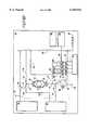
- a preferred enclosable single vessel system useful in the methods of the present invention that is capable of, for example, directly displacing one process liquid with another process liquid, and forming process liquids in-lineis shown in the FIGURE.
- the FIGUREshows an enclosable single vessel system 10 useful in the methods of the present invention.
- the single vessel system 10includes the following: a vessel module 2, a drying fluid module 50 for supplying a drying fluid stream 64 to vessel module 2, a pumping module 52 for pumping process fluid from and to vessel module 2, an injection module 54, a deionized water mix module 56, and a gas control unit 58 for controlling the level of gases in the deionized water.
- the vessel module 2contains a process vessel 20 having a support (not shown) for holding wafers 22, and top and bottom fluid ports 24, 26 respectively.
- the deionized water mix moduleprovides a stream of deionized water 30 that can optionally be further subdivided into deionized water streams 30A, 30B, 30C, and 30D.
- the injection module 54supplies one or more chemical streams 32A, 32B, 32C, and 32D to the vessel module 2.
- one or more chemical streams 32A, 32B, 32C, and 32Dmay optionally be combined at mixing valves 36A through 36D with deionized water streams 30A, 30B, 30C, and 30D respectively.
- the resulting one or more diluted chemical streamsmay then be directed into the process vessel 20 via valve 17 as process fluid stream 38.
- process fluid stream 38may contain deionized water alone, one or more chemicals, or a mixture of deionized water and one or more chemicals.
- such an injection module 54can provide point of use mixing as previously described herein.
- process fluid stream 38maybe directed to drain 98 via drain line 96 with bleed valve 18 open and valve 17 closed.
- Process fluid stream 38preferably enters process vessel 20 via line 25, through bottom fluid port 26, contacts wafers 22, and then exits top fluid port 24 via line 23. It is also possible to feed the process fluid stream 38 from top to bottom. Depending on the desired treatment, the process fluid exiting top fluid port 24 may then be directed to line 95, drain line 96 and drain 98 with valve 16 open and valve 12 closed. Pumping module 52 can be used for flushing deionized water 30 through the system lines via streams 53 and 55.
- Gas control unit 58is used to control the level of gases such as oxygen in the deionized water prior to being delivered to process vessel 20.
- the gas control unituses a Liqui-Cel® gas-liquid contactor manufactured by the Separation Products Group of Hoechst Celanese Corporation, Charlotte, N.C.
- the gas control unithas the capacity to pull and maintain a vacuum in a controlled fashion, add additional gases in a controlled fashion, and can handle process liquids having various flow rates. Further detail on suitable gas control units, and the operation of such units is disclosed in for example U.S. application Ser. No. 09/253,157, filed Feb. 19, 1999, the disclosure of which is hereby incorporated by reference in its entirety.
- the drying fluid module 50supplies a drying fluid stream 64 to process vessel 20 via valves 65 and 12 (with valve 16 closed).
- drying fluid stream 64is preferably fed to the process vessel 20 from top fluid port 24. Drying can be accomplished with the process vessel initially full of process fluid by directing the drying fluid stream 64, through valve 65 and valve 12 through top fluid port 24 and into process vessel 20. As the drying fluid stream displaces the process fluid, the drying fluid stream preferably mixes with the process fluid and forms a distinctive drying fluid layer (not shown) on top of the process fluid.
- the process fluid and drying fluid layerexits process vessel 20 through line 25 and is then directed through valves 14, 78, 79, and 81.
- a drain pump 80may optionally be used to allow better control of the descent rate of the process fluid and drying fluid stream to optimize drying.
- Valve 82is used to either direct the process fluid/drying fluid stream to a drying fluid recovery system (not shown) via line 83, or to drain 98 via line 85.
- the electronic componentsmay be removed from the vessel and further processed in any desired manner.
Landscapes
- Chemical & Material Sciences (AREA)
- Engineering & Computer Science (AREA)
- General Chemical & Material Sciences (AREA)
- Chemical Kinetics & Catalysis (AREA)
- Materials Engineering (AREA)
- Mechanical Engineering (AREA)
- Metallurgy (AREA)
- Organic Chemistry (AREA)
- Physics & Mathematics (AREA)
- Condensed Matter Physics & Semiconductors (AREA)
- General Physics & Mathematics (AREA)
- Manufacturing & Machinery (AREA)
- Computer Hardware Design (AREA)
- Microelectronics & Electronic Packaging (AREA)
- Power Engineering (AREA)
- Electrochemistry (AREA)
- Chemically Coating (AREA)
- Electrodes Of Semiconductors (AREA)
Abstract
Description
CH.sub.2 O+2OH→HCOO.sup.- +H.sub.ad +H.sub.2 O+e.sup.-(Eqn. 1)
2H.sub.ad →H.sub.2 (Eqn. 2) or
H.sub.ad +OH.sup.- →H.sub.2 O+e.sup.- (Eqn. 3)
Cu.sup.++ +2e.sup.- →Cu.sup.0 (Eqn. 4)
Cu.sup.+ +e.sup.- →Cu.sup.0 (Eqn. 5)
TABLE 1 ______________________________________ Preferred Compositions of Activation Solution Component in Activation Solution Amount ______________________________________ PdCl.sub.2 0.05 g/l to 0.8 g/l HCl 0.1 ml to 2 ml CH.sub.3 COOH 100 ml to 900 ml HF (50:1 volume, H.sub.2 O:HF) 50 ml to 500 ml H.sub.2O 50 ml to 500 ml ______________________________________
TABLE II ______________________________________ Examples of Compositions of Metal Deposition Solutions Metal pH Metal Ion Reducing Metal Adjusting Deposited Source Agent Complexant Additive ______________________________________ Cu about about about 0.01 M NaOH to 0.005 M 0.5 M to to about adjust pH to about about 5 M 0.15 M to about 0.05 M HCHO disodium 10.5 CuSO.sub.4 tartrate to about 12.5 Ni about about 0.5 g/l about 5.0 g/l NH.sub.4 OH 20.0 g/l to about to about to to about 4.0 g/l 35.0 g/l adjust the 60.0 g/l dimethyl sodium pH from NiSO.sub.4 6H.sub.2 O amine citrate about 5 borane to 7 Co about 5.0 g/l about 1.0 g/l about 15.0 g/l NH.sub.4 OH to to about to about to about adjust the 30.0 g/l 8.0 g/l 65.0 g/l pH from CoSO.sub.4 7H.sub.2 O dimethyl sodium about amine succinate 4.5 to 7.5 borane (6H.sub.2 O) CoWP about 5.0 g/l about 5.0 g/l about 40.0 g/l to trimethyl to about to about 120.0 g/l of ammonium 60.0 g/l 40.0 g/l Na.sub.3 C.sub.6 H.sub.4 O.sub.7 2H.sub.2 0 hydroxide CoCl.sub.2 6H.sub.2 O Na.sub.2 H.sub.2 PO.sub.2 and KOH and about to adjust 1.0 g/l pH to 9 to about to 9.6 20.0 g/l (NH.sub.4).sub.2 WO.sub.4 ______________________________________
Claims (20)
Priority Applications (8)
| Application Number | Priority Date | Filing Date | Title |
|---|---|---|---|
| US09/395,398US6165912A (en) | 1998-09-17 | 1999-09-14 | Electroless metal deposition of electronic components in an enclosable vessel |
| EP99969047AEP1115503A1 (en) | 1998-09-17 | 1999-09-16 | Electroless metal deposition of electronic components in an enclosable vessel |
| AU60437/99AAU6043799A (en) | 1998-09-17 | 1999-09-16 | Electroless metal deposition of electronic components in an enclosable vessel |
| CN99810935ACN1317997A (en) | 1998-09-17 | 1999-09-16 | Electroless metal deposition of electronic components in enclosable vessel |
| KR1020017003504AKR20010073173A (en) | 1998-09-17 | 1999-09-16 | Electroless Metal Deposition of Electronic Components in an Enclosable Vessel |
| PCT/US1999/021339WO2000015352A1 (en) | 1998-09-17 | 1999-09-16 | Electroless metal deposition of electronic components in an enclosable vessel |
| JP2000569928AJP2002524663A (en) | 1998-09-17 | 1999-09-16 | Electroless metal plating of electronic components in sealable containers |
| TW088116083ATW467767B (en) | 1998-09-17 | 1999-09-17 | Electroless metal deposition of electronic components in an enclosable vessel |
Applications Claiming Priority (2)
| Application Number | Priority Date | Filing Date | Title |
|---|---|---|---|
| US10087098P | 1998-09-17 | 1998-09-17 | |
| US09/395,398US6165912A (en) | 1998-09-17 | 1999-09-14 | Electroless metal deposition of electronic components in an enclosable vessel |
Publications (1)
| Publication Number | Publication Date |
|---|---|
| US6165912Atrue US6165912A (en) | 2000-12-26 |
Family
ID=26797637
Family Applications (1)
| Application Number | Title | Priority Date | Filing Date |
|---|---|---|---|
| US09/395,398Expired - Fee RelatedUS6165912A (en) | 1998-09-17 | 1999-09-14 | Electroless metal deposition of electronic components in an enclosable vessel |
Country Status (8)
| Country | Link |
|---|---|
| US (1) | US6165912A (en) |
| EP (1) | EP1115503A1 (en) |
| JP (1) | JP2002524663A (en) |
| KR (1) | KR20010073173A (en) |
| CN (1) | CN1317997A (en) |
| AU (1) | AU6043799A (en) |
| TW (1) | TW467767B (en) |
| WO (1) | WO2000015352A1 (en) |
Cited By (205)
| Publication number | Priority date | Publication date | Assignee | Title |
|---|---|---|---|---|
| US6391477B1 (en)* | 2000-07-06 | 2002-05-21 | Honeywell International Inc. | Electroless autocatalytic platinum plating |
| US6444583B2 (en)* | 1998-09-07 | 2002-09-03 | Nec Corporation | Substrate-cleaning method and substrate-cleaning solution |
| WO2002068717A1 (en)* | 2001-02-23 | 2002-09-06 | Scp Global Technologies | Method for etching electronic components containing tantalum |
| US20030017998A1 (en)* | 1997-05-16 | 2003-01-23 | Snow Alan D. | Proanthocyanidins for the treatment of amyloid and alpha-synuclein diseases |
| US6573183B2 (en) | 2001-09-28 | 2003-06-03 | Agere Systems Inc. | Method and apparatus for controlling contamination during the electroplating deposition of metals onto a semiconductor wafer surface |
| US20030190812A1 (en)* | 2002-04-03 | 2003-10-09 | Deenesh Padhi | Electroless deposition method |
| US20030189026A1 (en)* | 2002-04-03 | 2003-10-09 | Deenesh Padhi | Electroless deposition method |
| US20030190426A1 (en)* | 2002-04-03 | 2003-10-09 | Deenesh Padhi | Electroless deposition method |
| US20030188765A1 (en)* | 2002-04-03 | 2003-10-09 | Christenson Kurt Karl | Transition flow treatment process and apparatus |
| US20040018308A1 (en)* | 2001-12-14 | 2004-01-29 | Shipley Company, L.L.C. | Plating method |
| US20040033687A1 (en)* | 2002-08-19 | 2004-02-19 | Nishant Sinha | Activation of oxides for electroless plating |
| US6703712B2 (en) | 2001-11-13 | 2004-03-09 | Agere Systems, Inc. | Microelectronic device layer deposited with multiple electrolytes |
| US20040065540A1 (en)* | 2002-06-28 | 2004-04-08 | Novellus Systems, Inc. | Liquid treatment using thin liquid layer |
| US20040087141A1 (en)* | 2002-10-30 | 2004-05-06 | Applied Materials, Inc. | Post rinse to improve selective deposition of electroless cobalt on copper for ULSI application |
| US20040086656A1 (en)* | 2001-11-06 | 2004-05-06 | Kohl Paul A. | Electroless copper plating solutions and methods of use thereof |
| US6821324B2 (en)* | 2002-06-19 | 2004-11-23 | Ramot At Tel-Aviv University Ltd. | Cobalt tungsten phosphorus electroless deposition process and materials |
| US20050009340A1 (en)* | 2003-07-07 | 2005-01-13 | Yasuhiko Saijo | Method and apparatus for forming capping film |
| US20050022909A1 (en)* | 2003-03-20 | 2005-02-03 | Xinming Wang | Substrate processing method and substrate processing apparatus |
| US20050081785A1 (en)* | 2003-10-15 | 2005-04-21 | Applied Materials, Inc. | Apparatus for electroless deposition |
| US20050164497A1 (en)* | 2004-01-26 | 2005-07-28 | Sergey Lopatin | Pretreatment for electroless deposition |
| US20050227488A1 (en)* | 2004-03-31 | 2005-10-13 | O'brien Kevin P | Capping of copper structures in hydrophobic ILD using aqueous electro-less bath |
| US20060035016A1 (en)* | 2004-08-11 | 2006-02-16 | Chandra Tiwari | Electroless metal deposition methods |
| US7064065B2 (en) | 2003-10-15 | 2006-06-20 | Applied Materials, Inc. | Silver under-layers for electroless cobalt alloys |
| US20060165892A1 (en)* | 2005-01-27 | 2006-07-27 | Applied Materials, Inc. | Ruthenium containing layer deposition method |
| US7205233B2 (en) | 2003-11-07 | 2007-04-17 | Applied Materials, Inc. | Method for forming CoWRe alloys by electroless deposition |
| US20070218191A1 (en)* | 2006-03-10 | 2007-09-20 | Seiko Epson Corporation | Method for manufacturing wiring substrate |
| US20080057706A1 (en)* | 2006-08-30 | 2008-03-06 | Gyu Hyun Kim | Method for forming cyclinder type storage node for preventing creation of watermarks |
| US20080138508A1 (en)* | 2005-03-07 | 2008-06-12 | Daisuke Takagi | Substrate Processing Method and Substrate Processing Apparatus |
| US20080175986A1 (en)* | 2007-01-24 | 2008-07-24 | Kenneth Crouse | Second surface metallization |
| US7514353B2 (en) | 2005-03-18 | 2009-04-07 | Applied Materials, Inc. | Contact metallization scheme using a barrier layer over a silicide layer |
| US20090253262A1 (en)* | 2005-10-14 | 2009-10-08 | Blue29, Llc | Electroless plating system |
| US20090288593A1 (en)* | 2005-09-30 | 2009-11-26 | Blue 29, Llc | Electroless deposition system |
| US7651934B2 (en) | 2005-03-18 | 2010-01-26 | Applied Materials, Inc. | Process for electroless copper deposition |
| US7654221B2 (en) | 2003-10-06 | 2010-02-02 | Applied Materials, Inc. | Apparatus for electroless deposition of metals onto semiconductor substrates |
| US7659203B2 (en) | 2005-03-18 | 2010-02-09 | Applied Materials, Inc. | Electroless deposition process on a silicon contact |
| US7690324B1 (en) | 2002-06-28 | 2010-04-06 | Novellus Systems, Inc. | Small-volume electroless plating cell |
| US20100203731A1 (en)* | 2009-02-09 | 2010-08-12 | Bob Kong | Formation of a Zinc Passivation Layer on Titanium or Titanium Alloys Used in Semiconductor Processing |
| US7867900B2 (en) | 2007-09-28 | 2011-01-11 | Applied Materials, Inc. | Aluminum contact integration on cobalt silicide junction |
| US7981508B1 (en)* | 2006-09-12 | 2011-07-19 | Sri International | Flexible circuits |
| US7989029B1 (en) | 2007-06-21 | 2011-08-02 | Sri International | Reduced porosity copper deposition |
| US8110254B1 (en)* | 2006-09-12 | 2012-02-07 | Sri International | Flexible circuit chemistry |
| US8257781B1 (en) | 2002-06-28 | 2012-09-04 | Novellus Systems, Inc. | Electroless plating-liquid system |
| EP2407576A4 (en)* | 2009-03-13 | 2013-02-20 | Adeka Corp | METHOD FOR REMOVING WASTE WATER MOLECULES IN A PROCESS FOR PRODUCING THIN METAL FILM, AND PURGE SOLVENT |
| US8413320B2 (en) | 2011-01-28 | 2013-04-09 | Raytheon Company | Method of gold removal from electronic components |
| US8628818B1 (en)* | 2007-06-21 | 2014-01-14 | Sri International | Conductive pattern formation |
| US8679982B2 (en) | 2011-08-26 | 2014-03-25 | Applied Materials, Inc. | Selective suppression of dry-etch rate of materials containing both silicon and oxygen |
| US8679983B2 (en) | 2011-09-01 | 2014-03-25 | Applied Materials, Inc. | Selective suppression of dry-etch rate of materials containing both silicon and nitrogen |
| US20140154406A1 (en)* | 2012-11-30 | 2014-06-05 | Lam Research Corporation | Wet activation of ruthenium containing liner/barrier |
| US8754133B2 (en) | 2001-11-02 | 2014-06-17 | Proteotech, Inc. | Compounds, compositions and methods for the treatment of inflammatory diseases |
| US8765574B2 (en) | 2012-11-09 | 2014-07-01 | Applied Materials, Inc. | Dry etch process |
| US8771539B2 (en) | 2011-02-22 | 2014-07-08 | Applied Materials, Inc. | Remotely-excited fluorine and water vapor etch |
| US8801952B1 (en) | 2013-03-07 | 2014-08-12 | Applied Materials, Inc. | Conformal oxide dry etch |
| US8808563B2 (en) | 2011-10-07 | 2014-08-19 | Applied Materials, Inc. | Selective etch of silicon by way of metastable hydrogen termination |
| US8846163B2 (en) | 2004-02-26 | 2014-09-30 | Applied Materials, Inc. | Method for removing oxides |
| US8895874B1 (en) | 2009-03-10 | 2014-11-25 | Averatek Corp. | Indium-less transparent metalized layers |
| US8895449B1 (en) | 2013-05-16 | 2014-11-25 | Applied Materials, Inc. | Delicate dry clean |
| US8921234B2 (en) | 2012-12-21 | 2014-12-30 | Applied Materials, Inc. | Selective titanium nitride etching |
| US8927390B2 (en) | 2011-09-26 | 2015-01-06 | Applied Materials, Inc. | Intrench profile |
| US8951429B1 (en) | 2013-10-29 | 2015-02-10 | Applied Materials, Inc. | Tungsten oxide processing |
| US8956980B1 (en) | 2013-09-16 | 2015-02-17 | Applied Materials, Inc. | Selective etch of silicon nitride |
| US8969212B2 (en) | 2012-11-20 | 2015-03-03 | Applied Materials, Inc. | Dry-etch selectivity |
| US8975152B2 (en) | 2011-11-08 | 2015-03-10 | Applied Materials, Inc. | Methods of reducing substrate dislocation during gapfill processing |
| US8980763B2 (en) | 2012-11-30 | 2015-03-17 | Applied Materials, Inc. | Dry-etch for selective tungsten removal |
| US8999856B2 (en) | 2011-03-14 | 2015-04-07 | Applied Materials, Inc. | Methods for etch of sin films |
| US9023732B2 (en) | 2013-03-15 | 2015-05-05 | Applied Materials, Inc. | Processing systems and methods for halide scavenging |
| US9023734B2 (en) | 2012-09-18 | 2015-05-05 | Applied Materials, Inc. | Radical-component oxide etch |
| US9034770B2 (en) | 2012-09-17 | 2015-05-19 | Applied Materials, Inc. | Differential silicon oxide etch |
| US9040422B2 (en) | 2013-03-05 | 2015-05-26 | Applied Materials, Inc. | Selective titanium nitride removal |
| US20150155175A1 (en)* | 2013-11-29 | 2015-06-04 | Commissariat A L'energie Atomique Et Aux Ene Alt | Method for the metallization of a porous material |
| US20150162289A1 (en)* | 2013-12-09 | 2015-06-11 | Taiwan Semiconductor Manufacturing Company, Ltd. | Protective Layer for Contact Pads in Fan-out Interconnect Structure and Method of Forming Same |
| US9064816B2 (en) | 2012-11-30 | 2015-06-23 | Applied Materials, Inc. | Dry-etch for selective oxidation removal |
| US9064815B2 (en) | 2011-03-14 | 2015-06-23 | Applied Materials, Inc. | Methods for etch of metal and metal-oxide films |
| US9111877B2 (en) | 2012-12-18 | 2015-08-18 | Applied Materials, Inc. | Non-local plasma oxide etch |
| US9117855B2 (en) | 2013-12-04 | 2015-08-25 | Applied Materials, Inc. | Polarity control for remote plasma |
| US9114438B2 (en) | 2013-05-21 | 2015-08-25 | Applied Materials, Inc. | Copper residue chamber clean |
| US9132436B2 (en) | 2012-09-21 | 2015-09-15 | Applied Materials, Inc. | Chemical control features in wafer process equipment |
| US9136273B1 (en) | 2014-03-21 | 2015-09-15 | Applied Materials, Inc. | Flash gate air gap |
| US9159606B1 (en) | 2014-07-31 | 2015-10-13 | Applied Materials, Inc. | Metal air gap |
| US9165786B1 (en) | 2014-08-05 | 2015-10-20 | Applied Materials, Inc. | Integrated oxide and nitride recess for better channel contact in 3D architectures |
| US9190293B2 (en) | 2013-12-18 | 2015-11-17 | Applied Materials, Inc. | Even tungsten etch for high aspect ratio trenches |
| US9236266B2 (en) | 2011-08-01 | 2016-01-12 | Applied Materials, Inc. | Dry-etch for silicon-and-carbon-containing films |
| US9236265B2 (en) | 2013-11-04 | 2016-01-12 | Applied Materials, Inc. | Silicon germanium processing |
| US9245762B2 (en) | 2013-12-02 | 2016-01-26 | Applied Materials, Inc. | Procedure for etch rate consistency |
| US20160040294A1 (en)* | 2014-08-08 | 2016-02-11 | Uni-Pixel Displays, Inc. | Method of controlling oxygen levels for electroless plating of catalytic fine lines or features |
| US9263278B2 (en) | 2013-12-17 | 2016-02-16 | Applied Materials, Inc. | Dopant etch selectivity control |
| US9269590B2 (en) | 2014-04-07 | 2016-02-23 | Applied Materials, Inc. | Spacer formation |
| US9287134B2 (en) | 2014-01-17 | 2016-03-15 | Applied Materials, Inc. | Titanium oxide etch |
| US9287095B2 (en) | 2013-12-17 | 2016-03-15 | Applied Materials, Inc. | Semiconductor system assemblies and methods of operation |
| US9293568B2 (en) | 2014-01-27 | 2016-03-22 | Applied Materials, Inc. | Method of fin patterning |
| US9299537B2 (en) | 2014-03-20 | 2016-03-29 | Applied Materials, Inc. | Radial waveguide systems and methods for post-match control of microwaves |
| US9299582B2 (en) | 2013-11-12 | 2016-03-29 | Applied Materials, Inc. | Selective etch for metal-containing materials |
| US9299575B2 (en) | 2014-03-17 | 2016-03-29 | Applied Materials, Inc. | Gas-phase tungsten etch |
| US9299538B2 (en) | 2014-03-20 | 2016-03-29 | Applied Materials, Inc. | Radial waveguide systems and methods for post-match control of microwaves |
| US9299583B1 (en) | 2014-12-05 | 2016-03-29 | Applied Materials, Inc. | Aluminum oxide selective etch |
| US9309598B2 (en) | 2014-05-28 | 2016-04-12 | Applied Materials, Inc. | Oxide and metal removal |
| US9324576B2 (en) | 2010-05-27 | 2016-04-26 | Applied Materials, Inc. | Selective etch for silicon films |
| US9343272B1 (en) | 2015-01-08 | 2016-05-17 | Applied Materials, Inc. | Self-aligned process |
| US9349605B1 (en) | 2015-08-07 | 2016-05-24 | Applied Materials, Inc. | Oxide etch selectivity systems and methods |
| US9355862B2 (en) | 2014-09-24 | 2016-05-31 | Applied Materials, Inc. | Fluorine-based hardmask removal |
| US9355856B2 (en) | 2014-09-12 | 2016-05-31 | Applied Materials, Inc. | V trench dry etch |
| US9362130B2 (en) | 2013-03-01 | 2016-06-07 | Applied Materials, Inc. | Enhanced etching processes using remote plasma sources |
| US9368364B2 (en) | 2014-09-24 | 2016-06-14 | Applied Materials, Inc. | Silicon etch process with tunable selectivity to SiO2 and other materials |
| US9373517B2 (en) | 2012-08-02 | 2016-06-21 | Applied Materials, Inc. | Semiconductor processing with DC assisted RF power for improved control |
| US9373522B1 (en) | 2015-01-22 | 2016-06-21 | Applied Mateials, Inc. | Titanium nitride removal |
| US9378969B2 (en) | 2014-06-19 | 2016-06-28 | Applied Materials, Inc. | Low temperature gas-phase carbon removal |
| US9378978B2 (en) | 2014-07-31 | 2016-06-28 | Applied Materials, Inc. | Integrated oxide recess and floating gate fin trimming |
| US9385028B2 (en) | 2014-02-03 | 2016-07-05 | Applied Materials, Inc. | Air gap process |
| US9390937B2 (en) | 2012-09-20 | 2016-07-12 | Applied Materials, Inc. | Silicon-carbon-nitride selective etch |
| US9396989B2 (en) | 2014-01-27 | 2016-07-19 | Applied Materials, Inc. | Air gaps between copper lines |
| US9406523B2 (en) | 2014-06-19 | 2016-08-02 | Applied Materials, Inc. | Highly selective doped oxide removal method |
| US9425058B2 (en) | 2014-07-24 | 2016-08-23 | Applied Materials, Inc. | Simplified litho-etch-litho-etch process |
| US9449846B2 (en) | 2015-01-28 | 2016-09-20 | Applied Materials, Inc. | Vertical gate separation |
| US9478432B2 (en) | 2014-09-25 | 2016-10-25 | Applied Materials, Inc. | Silicon oxide selective removal |
| US9493879B2 (en) | 2013-07-12 | 2016-11-15 | Applied Materials, Inc. | Selective sputtering for pattern transfer |
| US9496167B2 (en) | 2014-07-31 | 2016-11-15 | Applied Materials, Inc. | Integrated bit-line airgap formation and gate stack post clean |
| US9499898B2 (en) | 2014-03-03 | 2016-11-22 | Applied Materials, Inc. | Layered thin film heater and method of fabrication |
| US9502258B2 (en) | 2014-12-23 | 2016-11-22 | Applied Materials, Inc. | Anisotropic gap etch |
| US9553102B2 (en) | 2014-08-19 | 2017-01-24 | Applied Materials, Inc. | Tungsten separation |
| US9576809B2 (en) | 2013-11-04 | 2017-02-21 | Applied Materials, Inc. | Etch suppression with germanium |
| US9659753B2 (en) | 2014-08-07 | 2017-05-23 | Applied Materials, Inc. | Grooved insulator to reduce leakage current |
| US9691645B2 (en) | 2015-08-06 | 2017-06-27 | Applied Materials, Inc. | Bolted wafer chuck thermal management systems and methods for wafer processing systems |
| US9721789B1 (en) | 2016-10-04 | 2017-08-01 | Applied Materials, Inc. | Saving ion-damaged spacers |
| US9728437B2 (en) | 2015-02-03 | 2017-08-08 | Applied Materials, Inc. | High temperature chuck for plasma processing systems |
| US9741593B2 (en) | 2015-08-06 | 2017-08-22 | Applied Materials, Inc. | Thermal management systems and methods for wafer processing systems |
| US9768034B1 (en) | 2016-11-11 | 2017-09-19 | Applied Materials, Inc. | Removal methods for high aspect ratio structures |
| US9773648B2 (en) | 2013-08-30 | 2017-09-26 | Applied Materials, Inc. | Dual discharge modes operation for remote plasma |
| US9847289B2 (en) | 2014-05-30 | 2017-12-19 | Applied Materials, Inc. | Protective via cap for improved interconnect performance |
| US9865484B1 (en) | 2016-06-29 | 2018-01-09 | Applied Materials, Inc. | Selective etch using material modification and RF pulsing |
| US9881805B2 (en) | 2015-03-02 | 2018-01-30 | Applied Materials, Inc. | Silicon selective removal |
| US9885117B2 (en) | 2014-03-31 | 2018-02-06 | Applied Materials, Inc. | Conditioned semiconductor system parts |
| US9934942B1 (en) | 2016-10-04 | 2018-04-03 | Applied Materials, Inc. | Chamber with flow-through source |
| US9947549B1 (en) | 2016-10-10 | 2018-04-17 | Applied Materials, Inc. | Cobalt-containing material removal |
| US10026621B2 (en) | 2016-11-14 | 2018-07-17 | Applied Materials, Inc. | SiN spacer profile patterning |
| US10043684B1 (en) | 2017-02-06 | 2018-08-07 | Applied Materials, Inc. | Self-limiting atomic thermal etching systems and methods |
| US10043674B1 (en) | 2017-08-04 | 2018-08-07 | Applied Materials, Inc. | Germanium etching systems and methods |
| US10049891B1 (en) | 2017-05-31 | 2018-08-14 | Applied Materials, Inc. | Selective in situ cobalt residue removal |
| US10062575B2 (en) | 2016-09-09 | 2018-08-28 | Applied Materials, Inc. | Poly directional etch by oxidation |
| US10062585B2 (en) | 2016-10-04 | 2018-08-28 | Applied Materials, Inc. | Oxygen compatible plasma source |
| US10062587B2 (en) | 2012-07-18 | 2018-08-28 | Applied Materials, Inc. | Pedestal with multi-zone temperature control and multiple purge capabilities |
| US10062579B2 (en) | 2016-10-07 | 2018-08-28 | Applied Materials, Inc. | Selective SiN lateral recess |
| US10128086B1 (en) | 2017-10-24 | 2018-11-13 | Applied Materials, Inc. | Silicon pretreatment for nitride removal |
| US10163696B2 (en) | 2016-11-11 | 2018-12-25 | Applied Materials, Inc. | Selective cobalt removal for bottom up gapfill |
| US10170336B1 (en) | 2017-08-04 | 2019-01-01 | Applied Materials, Inc. | Methods for anisotropic control of selective silicon removal |
| US10170282B2 (en) | 2013-03-08 | 2019-01-01 | Applied Materials, Inc. | Insulated semiconductor faceplate designs |
| US10224210B2 (en) | 2014-12-09 | 2019-03-05 | Applied Materials, Inc. | Plasma processing system with direct outlet toroidal plasma source |
| US10242908B2 (en) | 2016-11-14 | 2019-03-26 | Applied Materials, Inc. | Airgap formation with damage-free copper |
| US10256079B2 (en) | 2013-02-08 | 2019-04-09 | Applied Materials, Inc. | Semiconductor processing systems having multiple plasma configurations |
| US10256112B1 (en) | 2017-12-08 | 2019-04-09 | Applied Materials, Inc. | Selective tungsten removal |
| US10283321B2 (en) | 2011-01-18 | 2019-05-07 | Applied Materials, Inc. | Semiconductor processing system and methods using capacitively coupled plasma |
| US10283324B1 (en) | 2017-10-24 | 2019-05-07 | Applied Materials, Inc. | Oxygen treatment for nitride etching |
| US10297458B2 (en) | 2017-08-07 | 2019-05-21 | Applied Materials, Inc. | Process window widening using coated parts in plasma etch processes |
| US10319600B1 (en) | 2018-03-12 | 2019-06-11 | Applied Materials, Inc. | Thermal silicon etch |
| US10319649B2 (en) | 2017-04-11 | 2019-06-11 | Applied Materials, Inc. | Optical emission spectroscopy (OES) for remote plasma monitoring |
| US10319739B2 (en) | 2017-02-08 | 2019-06-11 | Applied Materials, Inc. | Accommodating imperfectly aligned memory holes |
| US10354889B2 (en) | 2017-07-17 | 2019-07-16 | Applied Materials, Inc. | Non-halogen etching of silicon-containing materials |
| US10403507B2 (en) | 2017-02-03 | 2019-09-03 | Applied Materials, Inc. | Shaped etch profile with oxidation |
| US10431429B2 (en) | 2017-02-03 | 2019-10-01 | Applied Materials, Inc. | Systems and methods for radial and azimuthal control of plasma uniformity |
| US10468267B2 (en) | 2017-05-31 | 2019-11-05 | Applied Materials, Inc. | Water-free etching methods |
| US10490406B2 (en) | 2018-04-10 | 2019-11-26 | Appled Materials, Inc. | Systems and methods for material breakthrough |
| US10490418B2 (en) | 2014-10-14 | 2019-11-26 | Applied Materials, Inc. | Systems and methods for internal surface conditioning assessment in plasma processing equipment |
| US10497573B2 (en) | 2018-03-13 | 2019-12-03 | Applied Materials, Inc. | Selective atomic layer etching of semiconductor materials |
| US10504700B2 (en) | 2015-08-27 | 2019-12-10 | Applied Materials, Inc. | Plasma etching systems and methods with secondary plasma injection |
| US10504754B2 (en) | 2016-05-19 | 2019-12-10 | Applied Materials, Inc. | Systems and methods for improved semiconductor etching and component protection |
| US10508351B2 (en)* | 2017-03-16 | 2019-12-17 | Lam Research Corporation | Layer-by-layer deposition using hydrogen |
| US10522371B2 (en) | 2016-05-19 | 2019-12-31 | Applied Materials, Inc. | Systems and methods for improved semiconductor etching and component protection |
| US10541246B2 (en) | 2017-06-26 | 2020-01-21 | Applied Materials, Inc. | 3D flash memory cells which discourage cross-cell electrical tunneling |
| US10541184B2 (en) | 2017-07-11 | 2020-01-21 | Applied Materials, Inc. | Optical emission spectroscopic techniques for monitoring etching |
| US10546729B2 (en) | 2016-10-04 | 2020-01-28 | Applied Materials, Inc. | Dual-channel showerhead with improved profile |
| US10566206B2 (en) | 2016-12-27 | 2020-02-18 | Applied Materials, Inc. | Systems and methods for anisotropic material breakthrough |
| US10573527B2 (en) | 2018-04-06 | 2020-02-25 | Applied Materials, Inc. | Gas-phase selective etching systems and methods |
| US10573496B2 (en) | 2014-12-09 | 2020-02-25 | Applied Materials, Inc. | Direct outlet toroidal plasma source |
| US10577692B2 (en)* | 2017-01-05 | 2020-03-03 | International Business Machines Corporation | Pretreatment of iron-based substrates for electroless plating |
| US10593523B2 (en) | 2014-10-14 | 2020-03-17 | Applied Materials, Inc. | Systems and methods for internal surface conditioning in plasma processing equipment |
| US10593560B2 (en) | 2018-03-01 | 2020-03-17 | Applied Materials, Inc. | Magnetic induction plasma source for semiconductor processes and equipment |
| US10615047B2 (en) | 2018-02-28 | 2020-04-07 | Applied Materials, Inc. | Systems and methods to form airgaps |
| US10629473B2 (en) | 2016-09-09 | 2020-04-21 | Applied Materials, Inc. | Footing removal for nitride spacer |
| US10672642B2 (en) | 2018-07-24 | 2020-06-02 | Applied Materials, Inc. | Systems and methods for pedestal configuration |
| US10679870B2 (en) | 2018-02-15 | 2020-06-09 | Applied Materials, Inc. | Semiconductor processing chamber multistage mixing apparatus |
| US10699879B2 (en) | 2018-04-17 | 2020-06-30 | Applied Materials, Inc. | Two piece electrode assembly with gap for plasma control |
| US10727080B2 (en) | 2017-07-07 | 2020-07-28 | Applied Materials, Inc. | Tantalum-containing material removal |
| US10755941B2 (en) | 2018-07-06 | 2020-08-25 | Applied Materials, Inc. | Self-limiting selective etching systems and methods |
| US10854426B2 (en) | 2018-01-08 | 2020-12-01 | Applied Materials, Inc. | Metal recess for semiconductor structures |
| US10872778B2 (en) | 2018-07-06 | 2020-12-22 | Applied Materials, Inc. | Systems and methods utilizing solid-phase etchants |
| US10886137B2 (en) | 2018-04-30 | 2021-01-05 | Applied Materials, Inc. | Selective nitride removal |
| US10892198B2 (en) | 2018-09-14 | 2021-01-12 | Applied Materials, Inc. | Systems and methods for improved performance in semiconductor processing |
| US10903054B2 (en) | 2017-12-19 | 2021-01-26 | Applied Materials, Inc. | Multi-zone gas distribution systems and methods |
| US10920320B2 (en) | 2017-06-16 | 2021-02-16 | Applied Materials, Inc. | Plasma health determination in semiconductor substrate processing reactors |
| US10920319B2 (en) | 2019-01-11 | 2021-02-16 | Applied Materials, Inc. | Ceramic showerheads with conductive electrodes |
| US10943834B2 (en) | 2017-03-13 | 2021-03-09 | Applied Materials, Inc. | Replacement contact process |
| US10964512B2 (en) | 2018-02-15 | 2021-03-30 | Applied Materials, Inc. | Semiconductor processing chamber multistage mixing apparatus and methods |
| US11049755B2 (en) | 2018-09-14 | 2021-06-29 | Applied Materials, Inc. | Semiconductor substrate supports with embedded RF shield |
| US11062887B2 (en) | 2018-09-17 | 2021-07-13 | Applied Materials, Inc. | High temperature RF heater pedestals |
| US11121002B2 (en) | 2018-10-24 | 2021-09-14 | Applied Materials, Inc. | Systems and methods for etching metals and metal derivatives |
| US11239061B2 (en) | 2014-11-26 | 2022-02-01 | Applied Materials, Inc. | Methods and systems to enhance process uniformity |
| US11257693B2 (en) | 2015-01-09 | 2022-02-22 | Applied Materials, Inc. | Methods and systems to improve pedestal temperature control |
| US11276590B2 (en) | 2017-05-17 | 2022-03-15 | Applied Materials, Inc. | Multi-zone semiconductor substrate supports |
| US11276559B2 (en) | 2017-05-17 | 2022-03-15 | Applied Materials, Inc. | Semiconductor processing chamber for multiple precursor flow |
| US11328909B2 (en) | 2017-12-22 | 2022-05-10 | Applied Materials, Inc. | Chamber conditioning and removal processes |
| US11417534B2 (en) | 2018-09-21 | 2022-08-16 | Applied Materials, Inc. | Selective material removal |
| US11437242B2 (en) | 2018-11-27 | 2022-09-06 | Applied Materials, Inc. | Selective removal of silicon-containing materials |
| US11594428B2 (en) | 2015-02-03 | 2023-02-28 | Applied Materials, Inc. | Low temperature chuck for plasma processing systems |
| US11682560B2 (en) | 2018-10-11 | 2023-06-20 | Applied Materials, Inc. | Systems and methods for hafnium-containing film removal |
| US11721527B2 (en) | 2019-01-07 | 2023-08-08 | Applied Materials, Inc. | Processing chamber mixing systems |
| US20240218519A1 (en)* | 2023-01-04 | 2024-07-04 | Applied Materials, Inc. | Electroless plating with a floating potential |
| US12340979B2 (en) | 2017-05-17 | 2025-06-24 | Applied Materials, Inc. | Semiconductor processing chamber for improved precursor flow |
Families Citing this family (2)
| Publication number | Priority date | Publication date | Assignee | Title |
|---|---|---|---|---|
| WO2003085166A2 (en)* | 2002-04-03 | 2003-10-16 | Applied Materials, Inc. | Electroless deposition methods |
| CN101152652B (en)* | 2006-09-29 | 2011-02-16 | 北京北方微电子基地设备工艺研究中心有限责任公司 | Method for cleaning surface of anodize parts |
Citations (33)
| Publication number | Priority date | Publication date | Assignee | Title |
|---|---|---|---|---|
| US3801368A (en)* | 1970-11-25 | 1974-04-02 | Toray Industries | Process of electroless plating and article made thereby |
| US4152467A (en)* | 1978-03-10 | 1979-05-01 | International Business Machines Corporation | Electroless copper plating process with dissolved oxygen maintained in bath |
| US4466864A (en)* | 1983-12-16 | 1984-08-21 | At&T Technologies, Inc. | Methods of and apparatus for electroplating preselected surface regions of electrical articles |
| US4574095A (en)* | 1984-11-19 | 1986-03-04 | International Business Machines Corporation | Selective deposition of copper |
| US4577650A (en)* | 1984-05-21 | 1986-03-25 | Mcconnell Christopher F | Vessel and system for treating wafers with fluids |
| US4633893A (en)* | 1984-05-21 | 1987-01-06 | Cfm Technologies Limited Partnership | Apparatus for treating semiconductor wafers |
| US4738272A (en)* | 1984-05-21 | 1988-04-19 | Mcconnell Christopher F | Vessel and system for treating wafers with fluids |
| US4778532A (en)* | 1985-06-24 | 1988-10-18 | Cfm Technologies Limited Partnership | Process and apparatus for treating wafers with process fluids |
| US4795497A (en)* | 1985-08-13 | 1989-01-03 | Mcconnell Christopher F | Method and system for fluid treatment of semiconductor wafers |
| US4885056A (en)* | 1988-09-02 | 1989-12-05 | Motorola Inc. | Method of reducing defects on semiconductor wafers |
| US4894260A (en)* | 1987-09-19 | 1990-01-16 | Pioneer Electronic Corporation | Electroless plating method and apparatus |
| US4899767A (en)* | 1984-05-21 | 1990-02-13 | Cfm Technologies, Inc. | Method and system for fluid treatment of semiconductor wafers |
| US4967690A (en)* | 1986-02-10 | 1990-11-06 | International Business Machines Corporation | Electroless plating with bi-level control of dissolved oxygen, with specific location of chemical maintenance means |
| US4984597A (en)* | 1984-05-21 | 1991-01-15 | Cfm Technologies Research Associates | Apparatus for rinsing and drying surfaces |
| US5071518A (en)* | 1989-10-24 | 1991-12-10 | Microelectronics And Computer Technology Corporation | Method of making an electrical multilayer interconnect |
| US5075259A (en)* | 1989-08-22 | 1991-12-24 | Motorola, Inc. | Method for forming semiconductor contacts by electroless plating |
| US5171709A (en)* | 1988-07-25 | 1992-12-15 | International Business Machines Corporation | Laser methods for circuit repair on integrated circuits and substrates |
| US5294572A (en)* | 1989-03-06 | 1994-03-15 | Asm International N.V. | Method and apparatus for depositing a layer on a substrate |
| US5308796A (en)* | 1991-09-30 | 1994-05-03 | At&T Bell Laboratories | Fabrication of electronic devices by electroless plating of copper onto a metal silicide |
| US5358907A (en)* | 1990-01-30 | 1994-10-25 | Xerox Corporation | Method of electrolessly depositing metals on a silicon substrate by immersing the substrate in hydrofluoric acid containing a buffered metal salt solution |
| US5383484A (en)* | 1993-07-16 | 1995-01-24 | Cfmt, Inc. | Static megasonic cleaning system for cleaning objects |
| US5424252A (en)* | 1991-10-04 | 1995-06-13 | Kabushiki Kaisha Toyota Chuo Kenkyusho | Photo-plating solution and process |
| US5544773A (en)* | 1991-09-06 | 1996-08-13 | Haruta; Youichi | Method for making multilayer printed circuit board having blind holes and resin-coated copper foil used for the method |
| US5569330A (en)* | 1994-04-15 | 1996-10-29 | Steag Microtech Gmbh Donaueschingen | Method and device for chemically treating substrates |
| US5571337A (en)* | 1994-11-14 | 1996-11-05 | Yieldup International | Method for cleaning and drying a semiconductor wafer |
| US5648125A (en)* | 1995-11-16 | 1997-07-15 | Cane; Frank N. | Electroless plating process for the manufacture of printed circuit boards |
| US5660706A (en)* | 1996-07-30 | 1997-08-26 | Sematech, Inc. | Electric field initiated electroless metal deposition |
| WO1998003273A1 (en)* | 1996-07-19 | 1998-01-29 | Cfmt, Inc. | Wet processing methods for the manufacture of electronic components using sequential chemical processing |
| US5743280A (en)* | 1995-12-19 | 1998-04-28 | Lg Semicon Co., Ltd. | Apparatus for cleansing semiconductor wafer |
| US5830805A (en)* | 1996-11-18 | 1998-11-03 | Cornell Research Foundation | Electroless deposition equipment or apparatus and method of performing electroless deposition |
| US5865894A (en)* | 1997-06-11 | 1999-02-02 | Reynolds Tech Fabricators, Inc. | Megasonic plating system |
| US5882498A (en)* | 1997-10-16 | 1999-03-16 | Advanced Micro Devices, Inc. | Method for reducing oxidation of electroplating chamber contacts and improving uniform electroplating of a substrate |
| WO1999030355A1 (en)* | 1997-12-10 | 1999-06-17 | Cfmt, Inc. | Wet processing methods for the manufacture of electronic components |
- 1999
- 1999-09-14USUS09/395,398patent/US6165912A/ennot_activeExpired - Fee Related
- 1999-09-16AUAU60437/99Apatent/AU6043799A/ennot_activeAbandoned
- 1999-09-16CNCN99810935Apatent/CN1317997A/enactivePending
- 1999-09-16KRKR1020017003504Apatent/KR20010073173A/ennot_activeWithdrawn
- 1999-09-16WOPCT/US1999/021339patent/WO2000015352A1/ennot_activeApplication Discontinuation
- 1999-09-16JPJP2000569928Apatent/JP2002524663A/enactivePending
- 1999-09-16EPEP99969047Apatent/EP1115503A1/ennot_activeWithdrawn
- 1999-09-17TWTW088116083Apatent/TW467767B/ennot_activeIP Right Cessation
Patent Citations (36)
| Publication number | Priority date | Publication date | Assignee | Title |
|---|---|---|---|---|
| US3801368A (en)* | 1970-11-25 | 1974-04-02 | Toray Industries | Process of electroless plating and article made thereby |
| US4152467A (en)* | 1978-03-10 | 1979-05-01 | International Business Machines Corporation | Electroless copper plating process with dissolved oxygen maintained in bath |
| US4466864A (en)* | 1983-12-16 | 1984-08-21 | At&T Technologies, Inc. | Methods of and apparatus for electroplating preselected surface regions of electrical articles |
| US4911761A (en)* | 1984-05-21 | 1990-03-27 | Cfm Technologies Research Associates | Process and apparatus for drying surfaces |
| US4917123A (en)* | 1984-05-21 | 1990-04-17 | Cfm Technologies Limited Partnership | Apparatus for treating wafers with process fluids |
| US4633893A (en)* | 1984-05-21 | 1987-01-06 | Cfm Technologies Limited Partnership | Apparatus for treating semiconductor wafers |
| US4738272A (en)* | 1984-05-21 | 1988-04-19 | Mcconnell Christopher F | Vessel and system for treating wafers with fluids |
| US4577650A (en)* | 1984-05-21 | 1986-03-25 | Mcconnell Christopher F | Vessel and system for treating wafers with fluids |
| US4984597B1 (en)* | 1984-05-21 | 1999-10-26 | Cfmt Inc | Apparatus for rinsing and drying surfaces |
| US4984597A (en)* | 1984-05-21 | 1991-01-15 | Cfm Technologies Research Associates | Apparatus for rinsing and drying surfaces |
| US4899767A (en)* | 1984-05-21 | 1990-02-13 | Cfm Technologies, Inc. | Method and system for fluid treatment of semiconductor wafers |
| US4574095A (en)* | 1984-11-19 | 1986-03-04 | International Business Machines Corporation | Selective deposition of copper |
| US4778532A (en)* | 1985-06-24 | 1988-10-18 | Cfm Technologies Limited Partnership | Process and apparatus for treating wafers with process fluids |
| US4795497A (en)* | 1985-08-13 | 1989-01-03 | Mcconnell Christopher F | Method and system for fluid treatment of semiconductor wafers |
| US4967690A (en)* | 1986-02-10 | 1990-11-06 | International Business Machines Corporation | Electroless plating with bi-level control of dissolved oxygen, with specific location of chemical maintenance means |
| US4894260A (en)* | 1987-09-19 | 1990-01-16 | Pioneer Electronic Corporation | Electroless plating method and apparatus |
| US5171709A (en)* | 1988-07-25 | 1992-12-15 | International Business Machines Corporation | Laser methods for circuit repair on integrated circuits and substrates |
| US4885056A (en)* | 1988-09-02 | 1989-12-05 | Motorola Inc. | Method of reducing defects on semiconductor wafers |
| US5294572A (en)* | 1989-03-06 | 1994-03-15 | Asm International N.V. | Method and apparatus for depositing a layer on a substrate |
| US5075259A (en)* | 1989-08-22 | 1991-12-24 | Motorola, Inc. | Method for forming semiconductor contacts by electroless plating |
| US5071518A (en)* | 1989-10-24 | 1991-12-10 | Microelectronics And Computer Technology Corporation | Method of making an electrical multilayer interconnect |
| US5358907A (en)* | 1990-01-30 | 1994-10-25 | Xerox Corporation | Method of electrolessly depositing metals on a silicon substrate by immersing the substrate in hydrofluoric acid containing a buffered metal salt solution |
| US5544773A (en)* | 1991-09-06 | 1996-08-13 | Haruta; Youichi | Method for making multilayer printed circuit board having blind holes and resin-coated copper foil used for the method |
| US5308796A (en)* | 1991-09-30 | 1994-05-03 | At&T Bell Laboratories | Fabrication of electronic devices by electroless plating of copper onto a metal silicide |
| US5424252A (en)* | 1991-10-04 | 1995-06-13 | Kabushiki Kaisha Toyota Chuo Kenkyusho | Photo-plating solution and process |
| US5383484A (en)* | 1993-07-16 | 1995-01-24 | Cfmt, Inc. | Static megasonic cleaning system for cleaning objects |
| US5569330A (en)* | 1994-04-15 | 1996-10-29 | Steag Microtech Gmbh Donaueschingen | Method and device for chemically treating substrates |
| US5571337A (en)* | 1994-11-14 | 1996-11-05 | Yieldup International | Method for cleaning and drying a semiconductor wafer |
| US5648125A (en)* | 1995-11-16 | 1997-07-15 | Cane; Frank N. | Electroless plating process for the manufacture of printed circuit boards |
| US5743280A (en)* | 1995-12-19 | 1998-04-28 | Lg Semicon Co., Ltd. | Apparatus for cleansing semiconductor wafer |
| WO1998003273A1 (en)* | 1996-07-19 | 1998-01-29 | Cfmt, Inc. | Wet processing methods for the manufacture of electronic components using sequential chemical processing |
| US5660706A (en)* | 1996-07-30 | 1997-08-26 | Sematech, Inc. | Electric field initiated electroless metal deposition |
| US5830805A (en)* | 1996-11-18 | 1998-11-03 | Cornell Research Foundation | Electroless deposition equipment or apparatus and method of performing electroless deposition |
| US5865894A (en)* | 1997-06-11 | 1999-02-02 | Reynolds Tech Fabricators, Inc. | Megasonic plating system |
| US5882498A (en)* | 1997-10-16 | 1999-03-16 | Advanced Micro Devices, Inc. | Method for reducing oxidation of electroplating chamber contacts and improving uniform electroplating of a substrate |
| WO1999030355A1 (en)* | 1997-12-10 | 1999-06-17 | Cfmt, Inc. | Wet processing methods for the manufacture of electronic components |
Non-Patent Citations (16)
| Title |
|---|
| "Full-Flow™ Wet Processing" brochure, 1993, CFM Technologies, Inc., West Chester, PA. |
| Full Flow Wet Processing brochure, 1993, CFM Technologies, Inc., West Chester, PA.* |
| Gale et al., "Experimental Study of Ultrasonic and Megasonic Particle Removal", Precision Cleaning, Apr. 1994, vol. 2, No. 4, 32 pages. |
| Gale et al., Experimental Study of Ultrasonic and Megasonic Particle Removal , Precision Cleaning, Apr. 1994, vol. 2, No. 4, 32 pages.* |
| Kern, W. et al., "Chemical Etching", Thin Film Processes, Vosser, J.L. (ed.), Academic Press, NY, 1978, vol. 1, pp. 403-447 and 452-481. |
| Kern, W. et al., Chemical Etching , Thin Film Processes , Vosser, J.L. (ed.), Academic Press, NY, 1978, vol. 1, pp. 403 447 and 452 481.* |
| Kirk Othmer Concise Encylcopedia of Chemical Technology, John Wiley & Sons, NY, 1985, 1142 1144.* |
| Kirk-Othmer Concise Encylcopedia of Chemical Technology, John Wiley & Sons, NY, 1985, 1142-1144. |
| Palmans, R. et al., "Development of an Electroless Copper Deposition Bath for Via Fill Applications on Tin Seed Layers," Conference Proceedings ULSI-X Materials Research Society, 1995, 87-94. |
| Palmans, R. et al., "Feasibility Study of Electroless Copper Deposition for VLSI," Applied Surface Science, 1991, 53, 345-352. |
| Palmans, R. et al., Development of an Electroless Copper Deposition Bath for Via Fill Applications on Tin Seed Layers, Conference Proceedings ULSI X Materials Research Society , 1995, 87 94.* |
| Palmans, R. et al., Feasibility Study of Electroless Copper Deposition for VLSI, Applied Surface Science , 1991, 53, 345 352.* |
| Ting, C.H. et al., "Selective Electroless Metal Deposition for via Hole Filling in VLSI Multilevel Interconnection Structures," J. Electrochem. Soc., 1989, 136(2), 462-466. |
| Ting, C.H. et al., Selective Electroless Metal Deposition for via Hole Filling in VLSI Multilevel Interconnection Structures, J. Electrochem. Soc. , 1989, 136(2), 462 466.* |
| Verhaverbeke, S. et al., "Scientific Rinsing and Drying on Macro and Microscale," in Semiconductor Pure Water and Chemicals Conference 1996, Balazs, m.K. (ed.), Santa Clara, CA Mar. 4-7, 1996, 14 pages. |
| Verhaverbeke, S. et al., Scientific Rinsing and Drying on Macro and Microscale, in Semiconductor Pure Water and Chemicals Conference 1996, Balazs, m.K. (ed.), Santa Clara, CA Mar. 4 7, 1996, 14 pages.* |
Cited By (309)
| Publication number | Priority date | Publication date | Assignee | Title |
|---|---|---|---|---|
| US20030017998A1 (en)* | 1997-05-16 | 2003-01-23 | Snow Alan D. | Proanthocyanidins for the treatment of amyloid and alpha-synuclein diseases |
| US6444583B2 (en)* | 1998-09-07 | 2002-09-03 | Nec Corporation | Substrate-cleaning method and substrate-cleaning solution |
| US6391477B1 (en)* | 2000-07-06 | 2002-05-21 | Honeywell International Inc. | Electroless autocatalytic platinum plating |
| WO2002068717A1 (en)* | 2001-02-23 | 2002-09-06 | Scp Global Technologies | Method for etching electronic components containing tantalum |
| US6573183B2 (en) | 2001-09-28 | 2003-06-03 | Agere Systems Inc. | Method and apparatus for controlling contamination during the electroplating deposition of metals onto a semiconductor wafer surface |
| US8754133B2 (en) | 2001-11-02 | 2014-06-17 | Proteotech, Inc. | Compounds, compositions and methods for the treatment of inflammatory diseases |
| US6875474B2 (en)* | 2001-11-06 | 2005-04-05 | Georgia Tech Research Corporation | Electroless copper plating solutions and methods of use thereof |
| US20040086656A1 (en)* | 2001-11-06 | 2004-05-06 | Kohl Paul A. | Electroless copper plating solutions and methods of use thereof |
| US6703712B2 (en) | 2001-11-13 | 2004-03-09 | Agere Systems, Inc. | Microelectronic device layer deposited with multiple electrolytes |
| US20040018308A1 (en)* | 2001-12-14 | 2004-01-29 | Shipley Company, L.L.C. | Plating method |
| US6911230B2 (en)* | 2001-12-14 | 2005-06-28 | Shipley Company, L.L.C. | Plating method |
| US20030189026A1 (en)* | 2002-04-03 | 2003-10-09 | Deenesh Padhi | Electroless deposition method |
| US20030190426A1 (en)* | 2002-04-03 | 2003-10-09 | Deenesh Padhi | Electroless deposition method |
| US20030188765A1 (en)* | 2002-04-03 | 2003-10-09 | Christenson Kurt Karl | Transition flow treatment process and apparatus |
| US20030190812A1 (en)* | 2002-04-03 | 2003-10-09 | Deenesh Padhi | Electroless deposition method |
| US6905622B2 (en) | 2002-04-03 | 2005-06-14 | Applied Materials, Inc. | Electroless deposition method |
| US7156927B2 (en) | 2002-04-03 | 2007-01-02 | Fsi International, Inc. | Transition flow treatment process and apparatus |
| US6899816B2 (en) | 2002-04-03 | 2005-05-31 | Applied Materials, Inc. | Electroless deposition method |
| US6821324B2 (en)* | 2002-06-19 | 2004-11-23 | Ramot At Tel-Aviv University Ltd. | Cobalt tungsten phosphorus electroless deposition process and materials |
| US8257781B1 (en) | 2002-06-28 | 2012-09-04 | Novellus Systems, Inc. | Electroless plating-liquid system |
| US7690324B1 (en) | 2002-06-28 | 2010-04-06 | Novellus Systems, Inc. | Small-volume electroless plating cell |
| US20040065540A1 (en)* | 2002-06-28 | 2004-04-08 | Novellus Systems, Inc. | Liquid treatment using thin liquid layer |
| US20050205933A1 (en)* | 2002-08-19 | 2005-09-22 | Nishant Sinha | Intermediate semiconductor device having activated oxide-based layer for electroless plating |
| US6900128B2 (en) | 2002-08-19 | 2005-05-31 | Micron Technology, Inc. | Activation of oxides for electroless plating |
| US20050023687A1 (en)* | 2002-08-19 | 2005-02-03 | Nishant Sinha | Activation of oxides for electroless plating |
| US20040033687A1 (en)* | 2002-08-19 | 2004-02-19 | Nishant Sinha | Activation of oxides for electroless plating |
| US6872659B2 (en) | 2002-08-19 | 2005-03-29 | Micron Technology, Inc. | Activation of oxides for electroless plating |
| US7042010B2 (en) | 2002-08-19 | 2006-05-09 | Micron Technology, Inc. | Intermediate semiconductor device having activated oxide-based layer for electroless plating |
| US6821909B2 (en)* | 2002-10-30 | 2004-11-23 | Applied Materials, Inc. | Post rinse to improve selective deposition of electroless cobalt on copper for ULSI application |
| US20040087141A1 (en)* | 2002-10-30 | 2004-05-06 | Applied Materials, Inc. | Post rinse to improve selective deposition of electroless cobalt on copper for ULSI application |
| US20050022909A1 (en)* | 2003-03-20 | 2005-02-03 | Xinming Wang | Substrate processing method and substrate processing apparatus |
| US20050009340A1 (en)* | 2003-07-07 | 2005-01-13 | Yasuhiko Saijo | Method and apparatus for forming capping film |
| US7654221B2 (en) | 2003-10-06 | 2010-02-02 | Applied Materials, Inc. | Apparatus for electroless deposition of metals onto semiconductor substrates |
| US7064065B2 (en) | 2003-10-15 | 2006-06-20 | Applied Materials, Inc. | Silver under-layers for electroless cobalt alloys |
| US7341633B2 (en) | 2003-10-15 | 2008-03-11 | Applied Materials, Inc. | Apparatus for electroless deposition |
| US20050081785A1 (en)* | 2003-10-15 | 2005-04-21 | Applied Materials, Inc. | Apparatus for electroless deposition |
| US7205233B2 (en) | 2003-11-07 | 2007-04-17 | Applied Materials, Inc. | Method for forming CoWRe alloys by electroless deposition |
| US20050164497A1 (en)* | 2004-01-26 | 2005-07-28 | Sergey Lopatin | Pretreatment for electroless deposition |
| US7256111B2 (en) | 2004-01-26 | 2007-08-14 | Applied Materials, Inc. | Pretreatment for electroless deposition |
| US8846163B2 (en) | 2004-02-26 | 2014-09-30 | Applied Materials, Inc. | Method for removing oxides |
| US20050227488A1 (en)* | 2004-03-31 | 2005-10-13 | O'brien Kevin P | Capping of copper structures in hydrophobic ILD using aqueous electro-less bath |
| US7119019B2 (en)* | 2004-03-31 | 2006-10-10 | Intel Corporation | Capping of copper structures in hydrophobic ILD using aqueous electro-less bath |
| US20070085162A1 (en)* | 2004-03-31 | 2007-04-19 | O'brien Kevin P | Capping of copper structures in hydrophobic ild using aqueous electro-less bath |
| US20060263528A1 (en)* | 2004-08-11 | 2006-11-23 | Chandra Tiwari | Electroless metal deposition methods |
| US20060035016A1 (en)* | 2004-08-11 | 2006-02-16 | Chandra Tiwari | Electroless metal deposition methods |
| US7438949B2 (en) | 2005-01-27 | 2008-10-21 | Applied Materials, Inc. | Ruthenium containing layer deposition method |
| US20060165892A1 (en)* | 2005-01-27 | 2006-07-27 | Applied Materials, Inc. | Ruthenium containing layer deposition method |
| US20080138508A1 (en)* | 2005-03-07 | 2008-06-12 | Daisuke Takagi | Substrate Processing Method and Substrate Processing Apparatus |
| US7514353B2 (en) | 2005-03-18 | 2009-04-07 | Applied Materials, Inc. | Contact metallization scheme using a barrier layer over a silicide layer |
| US7651934B2 (en) | 2005-03-18 | 2010-01-26 | Applied Materials, Inc. | Process for electroless copper deposition |
| US7659203B2 (en) | 2005-03-18 | 2010-02-09 | Applied Materials, Inc. | Electroless deposition process on a silicon contact |
| US8308858B2 (en) | 2005-03-18 | 2012-11-13 | Applied Materials, Inc. | Electroless deposition process on a silicon contact |
| US7913644B2 (en) | 2005-09-30 | 2011-03-29 | Lam Research Corporation | Electroless deposition system |
| US20090288593A1 (en)* | 2005-09-30 | 2009-11-26 | Blue 29, Llc | Electroless deposition system |
| US20110135824A1 (en)* | 2005-09-30 | 2011-06-09 | Ron Rulkens | Electroless Deposition System |
| US8622017B2 (en)* | 2005-10-14 | 2014-01-07 | Lam Research Corporation | Electroless plating system |
| US7972652B2 (en)* | 2005-10-14 | 2011-07-05 | Lam Research Corporation | Electroless plating system |
| US20090253262A1 (en)* | 2005-10-14 | 2009-10-08 | Blue29, Llc | Electroless plating system |
| US20110214608A1 (en)* | 2005-10-14 | 2011-09-08 | Igor Ivanov | Electroless Plating System |
| US20070218191A1 (en)* | 2006-03-10 | 2007-09-20 | Seiko Epson Corporation | Method for manufacturing wiring substrate |
| US20080057706A1 (en)* | 2006-08-30 | 2008-03-06 | Gyu Hyun Kim | Method for forming cyclinder type storage node for preventing creation of watermarks |
| US8911608B1 (en)* | 2006-09-12 | 2014-12-16 | Sri International | Flexible circuit formation |
| US7981508B1 (en)* | 2006-09-12 | 2011-07-19 | Sri International | Flexible circuits |
| US20110174524A1 (en)* | 2006-09-12 | 2011-07-21 | Sri International | Flexible circuits |
| US8110254B1 (en)* | 2006-09-12 | 2012-02-07 | Sri International | Flexible circuit chemistry |
| US8124226B2 (en) | 2006-09-12 | 2012-02-28 | Sri International | Flexible circuits |
| US20080175986A1 (en)* | 2007-01-24 | 2008-07-24 | Kenneth Crouse | Second surface metallization |
| US8628818B1 (en)* | 2007-06-21 | 2014-01-14 | Sri International | Conductive pattern formation |
| US7989029B1 (en) | 2007-06-21 | 2011-08-02 | Sri International | Reduced porosity copper deposition |
| US20140083748A1 (en)* | 2007-06-21 | 2014-03-27 | Sri International | Conductive pattern formation |
| US7867900B2 (en) | 2007-09-28 | 2011-01-11 | Applied Materials, Inc. | Aluminum contact integration on cobalt silicide junction |
| US8143164B2 (en)* | 2009-02-09 | 2012-03-27 | Intermolecular, Inc. | Formation of a zinc passivation layer on titanium or titanium alloys used in semiconductor processing |
| US20100203731A1 (en)* | 2009-02-09 | 2010-08-12 | Bob Kong | Formation of a Zinc Passivation Layer on Titanium or Titanium Alloys Used in Semiconductor Processing |
| US8895874B1 (en) | 2009-03-10 | 2014-11-25 | Averatek Corp. | Indium-less transparent metalized layers |
| EP2407576A4 (en)* | 2009-03-13 | 2013-02-20 | Adeka Corp | METHOD FOR REMOVING WASTE WATER MOLECULES IN A PROCESS FOR PRODUCING THIN METAL FILM, AND PURGE SOLVENT |
| US9754800B2 (en) | 2010-05-27 | 2017-09-05 | Applied Materials, Inc. | Selective etch for silicon films |
| US9324576B2 (en) | 2010-05-27 | 2016-04-26 | Applied Materials, Inc. | Selective etch for silicon films |
| US10283321B2 (en) | 2011-01-18 | 2019-05-07 | Applied Materials, Inc. | Semiconductor processing system and methods using capacitively coupled plasma |
| US8943662B2 (en) | 2011-01-28 | 2015-02-03 | Raytheon Company | Method for gold removal from electronic components |
| US8413320B2 (en) | 2011-01-28 | 2013-04-09 | Raytheon Company | Method of gold removal from electronic components |
| US8771539B2 (en) | 2011-02-22 | 2014-07-08 | Applied Materials, Inc. | Remotely-excited fluorine and water vapor etch |
| US8999856B2 (en) | 2011-03-14 | 2015-04-07 | Applied Materials, Inc. | Methods for etch of sin films |
| US9064815B2 (en) | 2011-03-14 | 2015-06-23 | Applied Materials, Inc. | Methods for etch of metal and metal-oxide films |
| US10062578B2 (en) | 2011-03-14 | 2018-08-28 | Applied Materials, Inc. | Methods for etch of metal and metal-oxide films |
| US9842744B2 (en) | 2011-03-14 | 2017-12-12 | Applied Materials, Inc. | Methods for etch of SiN films |
| US9236266B2 (en) | 2011-08-01 | 2016-01-12 | Applied Materials, Inc. | Dry-etch for silicon-and-carbon-containing films |
| US8679982B2 (en) | 2011-08-26 | 2014-03-25 | Applied Materials, Inc. | Selective suppression of dry-etch rate of materials containing both silicon and oxygen |
| US8679983B2 (en) | 2011-09-01 | 2014-03-25 | Applied Materials, Inc. | Selective suppression of dry-etch rate of materials containing both silicon and nitrogen |
| US8927390B2 (en) | 2011-09-26 | 2015-01-06 | Applied Materials, Inc. | Intrench profile |
| US9012302B2 (en) | 2011-09-26 | 2015-04-21 | Applied Materials, Inc. | Intrench profile |
| US9418858B2 (en) | 2011-10-07 | 2016-08-16 | Applied Materials, Inc. | Selective etch of silicon by way of metastable hydrogen termination |
| US8808563B2 (en) | 2011-10-07 | 2014-08-19 | Applied Materials, Inc. | Selective etch of silicon by way of metastable hydrogen termination |
| US8975152B2 (en) | 2011-11-08 | 2015-03-10 | Applied Materials, Inc. | Methods of reducing substrate dislocation during gapfill processing |
| US10062587B2 (en) | 2012-07-18 | 2018-08-28 | Applied Materials, Inc. | Pedestal with multi-zone temperature control and multiple purge capabilities |
| US10032606B2 (en) | 2012-08-02 | 2018-07-24 | Applied Materials, Inc. | Semiconductor processing with DC assisted RF power for improved control |
| US9373517B2 (en) | 2012-08-02 | 2016-06-21 | Applied Materials, Inc. | Semiconductor processing with DC assisted RF power for improved control |
| US9887096B2 (en) | 2012-09-17 | 2018-02-06 | Applied Materials, Inc. | Differential silicon oxide etch |
| US9034770B2 (en) | 2012-09-17 | 2015-05-19 | Applied Materials, Inc. | Differential silicon oxide etch |
| US9437451B2 (en) | 2012-09-18 | 2016-09-06 | Applied Materials, Inc. | Radical-component oxide etch |
| US9023734B2 (en) | 2012-09-18 | 2015-05-05 | Applied Materials, Inc. | Radical-component oxide etch |
| US9390937B2 (en) | 2012-09-20 | 2016-07-12 | Applied Materials, Inc. | Silicon-carbon-nitride selective etch |
| US10354843B2 (en) | 2012-09-21 | 2019-07-16 | Applied Materials, Inc. | Chemical control features in wafer process equipment |
| US11264213B2 (en) | 2012-09-21 | 2022-03-01 | Applied Materials, Inc. | Chemical control features in wafer process equipment |
| US9978564B2 (en) | 2012-09-21 | 2018-05-22 | Applied Materials, Inc. | Chemical control features in wafer process equipment |
| US9132436B2 (en) | 2012-09-21 | 2015-09-15 | Applied Materials, Inc. | Chemical control features in wafer process equipment |
| US8765574B2 (en) | 2012-11-09 | 2014-07-01 | Applied Materials, Inc. | Dry etch process |
| US8969212B2 (en) | 2012-11-20 | 2015-03-03 | Applied Materials, Inc. | Dry-etch selectivity |
| US9384997B2 (en) | 2012-11-20 | 2016-07-05 | Applied Materials, Inc. | Dry-etch selectivity |
| US20140154406A1 (en)* | 2012-11-30 | 2014-06-05 | Lam Research Corporation | Wet activation of ruthenium containing liner/barrier |
| US9412608B2 (en) | 2012-11-30 | 2016-08-09 | Applied Materials, Inc. | Dry-etch for selective tungsten removal |
| US9064816B2 (en) | 2012-11-30 | 2015-06-23 | Applied Materials, Inc. | Dry-etch for selective oxidation removal |
| US8980763B2 (en) | 2012-11-30 | 2015-03-17 | Applied Materials, Inc. | Dry-etch for selective tungsten removal |
| US9111877B2 (en) | 2012-12-18 | 2015-08-18 | Applied Materials, Inc. | Non-local plasma oxide etch |
| US9355863B2 (en) | 2012-12-18 | 2016-05-31 | Applied Materials, Inc. | Non-local plasma oxide etch |
| US9449845B2 (en) | 2012-12-21 | 2016-09-20 | Applied Materials, Inc. | Selective titanium nitride etching |
| US8921234B2 (en) | 2012-12-21 | 2014-12-30 | Applied Materials, Inc. | Selective titanium nitride etching |
| US10256079B2 (en) | 2013-02-08 | 2019-04-09 | Applied Materials, Inc. | Semiconductor processing systems having multiple plasma configurations |
| US11024486B2 (en) | 2013-02-08 | 2021-06-01 | Applied Materials, Inc. | Semiconductor processing systems having multiple plasma configurations |
| US9362130B2 (en) | 2013-03-01 | 2016-06-07 | Applied Materials, Inc. | Enhanced etching processes using remote plasma sources |
| US10424485B2 (en) | 2013-03-01 | 2019-09-24 | Applied Materials, Inc. | Enhanced etching processes using remote plasma sources |
| US9040422B2 (en) | 2013-03-05 | 2015-05-26 | Applied Materials, Inc. | Selective titanium nitride removal |
| US9607856B2 (en) | 2013-03-05 | 2017-03-28 | Applied Materials, Inc. | Selective titanium nitride removal |
| US8801952B1 (en) | 2013-03-07 | 2014-08-12 | Applied Materials, Inc. | Conformal oxide dry etch |
| US9093390B2 (en) | 2013-03-07 | 2015-07-28 | Applied Materials, Inc. | Conformal oxide dry etch |
| US10170282B2 (en) | 2013-03-08 | 2019-01-01 | Applied Materials, Inc. | Insulated semiconductor faceplate designs |
| US9449850B2 (en) | 2013-03-15 | 2016-09-20 | Applied Materials, Inc. | Processing systems and methods for halide scavenging |
| US9184055B2 (en) | 2013-03-15 | 2015-11-10 | Applied Materials, Inc. | Processing systems and methods for halide scavenging |
| US9659792B2 (en) | 2013-03-15 | 2017-05-23 | Applied Materials, Inc. | Processing systems and methods for halide scavenging |
| US9991134B2 (en) | 2013-03-15 | 2018-06-05 | Applied Materials, Inc. | Processing systems and methods for halide scavenging |
| US9704723B2 (en) | 2013-03-15 | 2017-07-11 | Applied Materials, Inc. | Processing systems and methods for halide scavenging |
| US9093371B2 (en) | 2013-03-15 | 2015-07-28 | Applied Materials, Inc. | Processing systems and methods for halide scavenging |
| US9023732B2 (en) | 2013-03-15 | 2015-05-05 | Applied Materials, Inc. | Processing systems and methods for halide scavenging |
| US9153442B2 (en) | 2013-03-15 | 2015-10-06 | Applied Materials, Inc. | Processing systems and methods for halide scavenging |
| US8895449B1 (en) | 2013-05-16 | 2014-11-25 | Applied Materials, Inc. | Delicate dry clean |
| US9114438B2 (en) | 2013-05-21 | 2015-08-25 | Applied Materials, Inc. | Copper residue chamber clean |
| US9493879B2 (en) | 2013-07-12 | 2016-11-15 | Applied Materials, Inc. | Selective sputtering for pattern transfer |
| US9773648B2 (en) | 2013-08-30 | 2017-09-26 | Applied Materials, Inc. | Dual discharge modes operation for remote plasma |
| US8956980B1 (en) | 2013-09-16 | 2015-02-17 | Applied Materials, Inc. | Selective etch of silicon nitride |
| US9209012B2 (en) | 2013-09-16 | 2015-12-08 | Applied Materials, Inc. | Selective etch of silicon nitride |
| US8951429B1 (en) | 2013-10-29 | 2015-02-10 | Applied Materials, Inc. | Tungsten oxide processing |
| US9236265B2 (en) | 2013-11-04 | 2016-01-12 | Applied Materials, Inc. | Silicon germanium processing |
| US9576809B2 (en) | 2013-11-04 | 2017-02-21 | Applied Materials, Inc. | Etch suppression with germanium |
| US9472417B2 (en) | 2013-11-12 | 2016-10-18 | Applied Materials, Inc. | Plasma-free metal etch |
| US9520303B2 (en) | 2013-11-12 | 2016-12-13 | Applied Materials, Inc. | Aluminum selective etch |
| US9711366B2 (en) | 2013-11-12 | 2017-07-18 | Applied Materials, Inc. | Selective etch for metal-containing materials |
| US9299582B2 (en) | 2013-11-12 | 2016-03-29 | Applied Materials, Inc. | Selective etch for metal-containing materials |
| US20150155175A1 (en)* | 2013-11-29 | 2015-06-04 | Commissariat A L'energie Atomique Et Aux Ene Alt | Method for the metallization of a porous material |
| US9472412B2 (en) | 2013-12-02 | 2016-10-18 | Applied Materials, Inc. | Procedure for etch rate consistency |
| US9245762B2 (en) | 2013-12-02 | 2016-01-26 | Applied Materials, Inc. | Procedure for etch rate consistency |
| US9117855B2 (en) | 2013-12-04 | 2015-08-25 | Applied Materials, Inc. | Polarity control for remote plasma |
| US9941244B2 (en)* | 2013-12-09 | 2018-04-10 | Taiwan Semiconductor Manufacturing Company, Ltd. | Protective layer for contact pads in fan-out interconnect structure and method of forming same |
| US20150162289A1 (en)* | 2013-12-09 | 2015-06-11 | Taiwan Semiconductor Manufacturing Company, Ltd. | Protective Layer for Contact Pads in Fan-out Interconnect Structure and Method of Forming Same |
| US10748869B2 (en) | 2013-12-09 | 2020-08-18 | Taiwan Semiconductor Manufacturing Company, Ltd. | Protective layer for contact pads in fan-out interconnect structure and method of forming same |
| US11515288B2 (en) | 2013-12-09 | 2022-11-29 | Taiwan Semiconductor Manufacturing Company, Ltd. | Protective layer for contact pads in fan-out interconnect structure and method of forming same |
| US9263278B2 (en) | 2013-12-17 | 2016-02-16 | Applied Materials, Inc. | Dopant etch selectivity control |
| US9287095B2 (en) | 2013-12-17 | 2016-03-15 | Applied Materials, Inc. | Semiconductor system assemblies and methods of operation |
| US9190293B2 (en) | 2013-12-18 | 2015-11-17 | Applied Materials, Inc. | Even tungsten etch for high aspect ratio trenches |
| US9287134B2 (en) | 2014-01-17 | 2016-03-15 | Applied Materials, Inc. | Titanium oxide etch |
| US9293568B2 (en) | 2014-01-27 | 2016-03-22 | Applied Materials, Inc. | Method of fin patterning |
| US9396989B2 (en) | 2014-01-27 | 2016-07-19 | Applied Materials, Inc. | Air gaps between copper lines |
| US9385028B2 (en) | 2014-02-03 | 2016-07-05 | Applied Materials, Inc. | Air gap process |
| US9499898B2 (en) | 2014-03-03 | 2016-11-22 | Applied Materials, Inc. | Layered thin film heater and method of fabrication |
| US9299575B2 (en) | 2014-03-17 | 2016-03-29 | Applied Materials, Inc. | Gas-phase tungsten etch |
| US9837249B2 (en) | 2014-03-20 | 2017-12-05 | Applied Materials, Inc. | Radial waveguide systems and methods for post-match control of microwaves |
| US9299538B2 (en) | 2014-03-20 | 2016-03-29 | Applied Materials, Inc. | Radial waveguide systems and methods for post-match control of microwaves |
| US9564296B2 (en) | 2014-03-20 | 2017-02-07 | Applied Materials, Inc. | Radial waveguide systems and methods for post-match control of microwaves |
| US9299537B2 (en) | 2014-03-20 | 2016-03-29 | Applied Materials, Inc. | Radial waveguide systems and methods for post-match control of microwaves |
| US9136273B1 (en) | 2014-03-21 | 2015-09-15 | Applied Materials, Inc. | Flash gate air gap |
| US9903020B2 (en) | 2014-03-31 | 2018-02-27 | Applied Materials, Inc. | Generation of compact alumina passivation layers on aluminum plasma equipment components |
| US9885117B2 (en) | 2014-03-31 | 2018-02-06 | Applied Materials, Inc. | Conditioned semiconductor system parts |
| US9269590B2 (en) | 2014-04-07 | 2016-02-23 | Applied Materials, Inc. | Spacer formation |
| US9309598B2 (en) | 2014-05-28 | 2016-04-12 | Applied Materials, Inc. | Oxide and metal removal |
| US10465294B2 (en) | 2014-05-28 | 2019-11-05 | Applied Materials, Inc. | Oxide and metal removal |
| US9847289B2 (en) | 2014-05-30 | 2017-12-19 | Applied Materials, Inc. | Protective via cap for improved interconnect performance |
| US9378969B2 (en) | 2014-06-19 | 2016-06-28 | Applied Materials, Inc. | Low temperature gas-phase carbon removal |
| US9406523B2 (en) | 2014-06-19 | 2016-08-02 | Applied Materials, Inc. | Highly selective doped oxide removal method |
| US9425058B2 (en) | 2014-07-24 | 2016-08-23 | Applied Materials, Inc. | Simplified litho-etch-litho-etch process |
| US9496167B2 (en) | 2014-07-31 | 2016-11-15 | Applied Materials, Inc. | Integrated bit-line airgap formation and gate stack post clean |
| US9773695B2 (en) | 2014-07-31 | 2017-09-26 | Applied Materials, Inc. | Integrated bit-line airgap formation and gate stack post clean |
| US9378978B2 (en) | 2014-07-31 | 2016-06-28 | Applied Materials, Inc. | Integrated oxide recess and floating gate fin trimming |
| US9159606B1 (en) | 2014-07-31 | 2015-10-13 | Applied Materials, Inc. | Metal air gap |
| US9165786B1 (en) | 2014-08-05 | 2015-10-20 | Applied Materials, Inc. | Integrated oxide and nitride recess for better channel contact in 3D architectures |
| US9659753B2 (en) | 2014-08-07 | 2017-05-23 | Applied Materials, Inc. | Grooved insulator to reduce leakage current |
| US20160040294A1 (en)* | 2014-08-08 | 2016-02-11 | Uni-Pixel Displays, Inc. | Method of controlling oxygen levels for electroless plating of catalytic fine lines or features |
| US9553102B2 (en) | 2014-08-19 | 2017-01-24 | Applied Materials, Inc. | Tungsten separation |
| US9355856B2 (en) | 2014-09-12 | 2016-05-31 | Applied Materials, Inc. | V trench dry etch |
| US9478434B2 (en) | 2014-09-24 | 2016-10-25 | Applied Materials, Inc. | Chlorine-based hardmask removal |
| US9355862B2 (en) | 2014-09-24 | 2016-05-31 | Applied Materials, Inc. | Fluorine-based hardmask removal |
| US9368364B2 (en) | 2014-09-24 | 2016-06-14 | Applied Materials, Inc. | Silicon etch process with tunable selectivity to SiO2 and other materials |
| US9478432B2 (en) | 2014-09-25 | 2016-10-25 | Applied Materials, Inc. | Silicon oxide selective removal |
| US9837284B2 (en) | 2014-09-25 | 2017-12-05 | Applied Materials, Inc. | Oxide etch selectivity enhancement |
| US9613822B2 (en) | 2014-09-25 | 2017-04-04 | Applied Materials, Inc. | Oxide etch selectivity enhancement |
| US10490418B2 (en) | 2014-10-14 | 2019-11-26 | Applied Materials, Inc. | Systems and methods for internal surface conditioning assessment in plasma processing equipment |
| US10796922B2 (en) | 2014-10-14 | 2020-10-06 | Applied Materials, Inc. | Systems and methods for internal surface conditioning assessment in plasma processing equipment |
| US10593523B2 (en) | 2014-10-14 | 2020-03-17 | Applied Materials, Inc. | Systems and methods for internal surface conditioning in plasma processing equipment |
| US10707061B2 (en) | 2014-10-14 | 2020-07-07 | Applied Materials, Inc. | Systems and methods for internal surface conditioning in plasma processing equipment |
| US11637002B2 (en) | 2014-11-26 | 2023-04-25 | Applied Materials, Inc. | Methods and systems to enhance process uniformity |
| US11239061B2 (en) | 2014-11-26 | 2022-02-01 | Applied Materials, Inc. | Methods and systems to enhance process uniformity |
| US9299583B1 (en) | 2014-12-05 | 2016-03-29 | Applied Materials, Inc. | Aluminum oxide selective etch |
| US10224210B2 (en) | 2014-12-09 | 2019-03-05 | Applied Materials, Inc. | Plasma processing system with direct outlet toroidal plasma source |
| US10573496B2 (en) | 2014-12-09 | 2020-02-25 | Applied Materials, Inc. | Direct outlet toroidal plasma source |
| US9502258B2 (en) | 2014-12-23 | 2016-11-22 | Applied Materials, Inc. | Anisotropic gap etch |
| US9343272B1 (en) | 2015-01-08 | 2016-05-17 | Applied Materials, Inc. | Self-aligned process |
| US11257693B2 (en) | 2015-01-09 | 2022-02-22 | Applied Materials, Inc. | Methods and systems to improve pedestal temperature control |
| US9373522B1 (en) | 2015-01-22 | 2016-06-21 | Applied Mateials, Inc. | Titanium nitride removal |
| US9449846B2 (en) | 2015-01-28 | 2016-09-20 | Applied Materials, Inc. | Vertical gate separation |
| US12009228B2 (en) | 2015-02-03 | 2024-06-11 | Applied Materials, Inc. | Low temperature chuck for plasma processing systems |
| US9728437B2 (en) | 2015-02-03 | 2017-08-08 | Applied Materials, Inc. | High temperature chuck for plasma processing systems |
| US11594428B2 (en) | 2015-02-03 | 2023-02-28 | Applied Materials, Inc. | Low temperature chuck for plasma processing systems |
| US10468285B2 (en) | 2015-02-03 | 2019-11-05 | Applied Materials, Inc. | High temperature chuck for plasma processing systems |
| US9881805B2 (en) | 2015-03-02 | 2018-01-30 | Applied Materials, Inc. | Silicon selective removal |
| US11158527B2 (en) | 2015-08-06 | 2021-10-26 | Applied Materials, Inc. | Thermal management systems and methods for wafer processing systems |
| US10468276B2 (en) | 2015-08-06 | 2019-11-05 | Applied Materials, Inc. | Thermal management systems and methods for wafer processing systems |
| US10607867B2 (en) | 2015-08-06 | 2020-03-31 | Applied Materials, Inc. | Bolted wafer chuck thermal management systems and methods for wafer processing systems |
| US9741593B2 (en) | 2015-08-06 | 2017-08-22 | Applied Materials, Inc. | Thermal management systems and methods for wafer processing systems |
| US10147620B2 (en) | 2015-08-06 | 2018-12-04 | Applied Materials, Inc. | Bolted wafer chuck thermal management systems and methods for wafer processing systems |
| US9691645B2 (en) | 2015-08-06 | 2017-06-27 | Applied Materials, Inc. | Bolted wafer chuck thermal management systems and methods for wafer processing systems |
| US10424463B2 (en) | 2015-08-07 | 2019-09-24 | Applied Materials, Inc. | Oxide etch selectivity systems and methods |
| US9349605B1 (en) | 2015-08-07 | 2016-05-24 | Applied Materials, Inc. | Oxide etch selectivity systems and methods |
| US10424464B2 (en) | 2015-08-07 | 2019-09-24 | Applied Materials, Inc. | Oxide etch selectivity systems and methods |
| US11476093B2 (en) | 2015-08-27 | 2022-10-18 | Applied Materials, Inc. | Plasma etching systems and methods with secondary plasma injection |
| US10504700B2 (en) | 2015-08-27 | 2019-12-10 | Applied Materials, Inc. | Plasma etching systems and methods with secondary plasma injection |
| US10504754B2 (en) | 2016-05-19 | 2019-12-10 | Applied Materials, Inc. | Systems and methods for improved semiconductor etching and component protection |
| US10522371B2 (en) | 2016-05-19 | 2019-12-31 | Applied Materials, Inc. | Systems and methods for improved semiconductor etching and component protection |
| US11735441B2 (en) | 2016-05-19 | 2023-08-22 | Applied Materials, Inc. | Systems and methods for improved semiconductor etching and component protection |
| US12057329B2 (en) | 2016-06-29 | 2024-08-06 | Applied Materials, Inc. | Selective etch using material modification and RF pulsing |
| US9865484B1 (en) | 2016-06-29 | 2018-01-09 | Applied Materials, Inc. | Selective etch using material modification and RF pulsing |
| US10062575B2 (en) | 2016-09-09 | 2018-08-28 | Applied Materials, Inc. | Poly directional etch by oxidation |
| US10629473B2 (en) | 2016-09-09 | 2020-04-21 | Applied Materials, Inc. | Footing removal for nitride spacer |
| US10546729B2 (en) | 2016-10-04 | 2020-01-28 | Applied Materials, Inc. | Dual-channel showerhead with improved profile |
| US10541113B2 (en) | 2016-10-04 | 2020-01-21 | Applied Materials, Inc. | Chamber with flow-through source |
| US9934942B1 (en) | 2016-10-04 | 2018-04-03 | Applied Materials, Inc. | Chamber with flow-through source |
| US10224180B2 (en) | 2016-10-04 | 2019-03-05 | Applied Materials, Inc. | Chamber with flow-through source |
| US11049698B2 (en) | 2016-10-04 | 2021-06-29 | Applied Materials, Inc. | Dual-channel showerhead with improved profile |
| US9721789B1 (en) | 2016-10-04 | 2017-08-01 | Applied Materials, Inc. | Saving ion-damaged spacers |
| US10062585B2 (en) | 2016-10-04 | 2018-08-28 | Applied Materials, Inc. | Oxygen compatible plasma source |
| US10062579B2 (en) | 2016-10-07 | 2018-08-28 | Applied Materials, Inc. | Selective SiN lateral recess |
| US10319603B2 (en) | 2016-10-07 | 2019-06-11 | Applied Materials, Inc. | Selective SiN lateral recess |
| US9947549B1 (en) | 2016-10-10 | 2018-04-17 | Applied Materials, Inc. | Cobalt-containing material removal |
| US10770346B2 (en) | 2016-11-11 | 2020-09-08 | Applied Materials, Inc. | Selective cobalt removal for bottom up gapfill |
| US10186428B2 (en) | 2016-11-11 | 2019-01-22 | Applied Materials, Inc. | Removal methods for high aspect ratio structures |
| US9768034B1 (en) | 2016-11-11 | 2017-09-19 | Applied Materials, Inc. | Removal methods for high aspect ratio structures |
| US10163696B2 (en) | 2016-11-11 | 2018-12-25 | Applied Materials, Inc. | Selective cobalt removal for bottom up gapfill |
| US10242908B2 (en) | 2016-11-14 | 2019-03-26 | Applied Materials, Inc. | Airgap formation with damage-free copper |
| US10026621B2 (en) | 2016-11-14 | 2018-07-17 | Applied Materials, Inc. | SiN spacer profile patterning |
| US10600639B2 (en) | 2016-11-14 | 2020-03-24 | Applied Materials, Inc. | SiN spacer profile patterning |
| US10566206B2 (en) | 2016-12-27 | 2020-02-18 | Applied Materials, Inc. | Systems and methods for anisotropic material breakthrough |
| US10577692B2 (en)* | 2017-01-05 | 2020-03-03 | International Business Machines Corporation | Pretreatment of iron-based substrates for electroless plating |
| US10903052B2 (en) | 2017-02-03 | 2021-01-26 | Applied Materials, Inc. | Systems and methods for radial and azimuthal control of plasma uniformity |
| US10431429B2 (en) | 2017-02-03 | 2019-10-01 | Applied Materials, Inc. | Systems and methods for radial and azimuthal control of plasma uniformity |
| US10403507B2 (en) | 2017-02-03 | 2019-09-03 | Applied Materials, Inc. | Shaped etch profile with oxidation |
| US10043684B1 (en) | 2017-02-06 | 2018-08-07 | Applied Materials, Inc. | Self-limiting atomic thermal etching systems and methods |
| US10319739B2 (en) | 2017-02-08 | 2019-06-11 | Applied Materials, Inc. | Accommodating imperfectly aligned memory holes |
| US10529737B2 (en) | 2017-02-08 | 2020-01-07 | Applied Materials, Inc. | Accommodating imperfectly aligned memory holes |
| US10325923B2 (en) | 2017-02-08 | 2019-06-18 | Applied Materials, Inc. | Accommodating imperfectly aligned memory holes |
| US10943834B2 (en) | 2017-03-13 | 2021-03-09 | Applied Materials, Inc. | Replacement contact process |
| US10508351B2 (en)* | 2017-03-16 | 2019-12-17 | Lam Research Corporation | Layer-by-layer deposition using hydrogen |
| US10319649B2 (en) | 2017-04-11 | 2019-06-11 | Applied Materials, Inc. | Optical emission spectroscopy (OES) for remote plasma monitoring |
| US11276559B2 (en) | 2017-05-17 | 2022-03-15 | Applied Materials, Inc. | Semiconductor processing chamber for multiple precursor flow |
| US11276590B2 (en) | 2017-05-17 | 2022-03-15 | Applied Materials, Inc. | Multi-zone semiconductor substrate supports |
| US11361939B2 (en) | 2017-05-17 | 2022-06-14 | Applied Materials, Inc. | Semiconductor processing chamber for multiple precursor flow |
| US11915950B2 (en) | 2017-05-17 | 2024-02-27 | Applied Materials, Inc. | Multi-zone semiconductor substrate supports |
| US12340979B2 (en) | 2017-05-17 | 2025-06-24 | Applied Materials, Inc. | Semiconductor processing chamber for improved precursor flow |
| US10497579B2 (en) | 2017-05-31 | 2019-12-03 | Applied Materials, Inc. | Water-free etching methods |
| US10468267B2 (en) | 2017-05-31 | 2019-11-05 | Applied Materials, Inc. | Water-free etching methods |
| US10049891B1 (en) | 2017-05-31 | 2018-08-14 | Applied Materials, Inc. | Selective in situ cobalt residue removal |
| US10920320B2 (en) | 2017-06-16 | 2021-02-16 | Applied Materials, Inc. | Plasma health determination in semiconductor substrate processing reactors |
| US10541246B2 (en) | 2017-06-26 | 2020-01-21 | Applied Materials, Inc. | 3D flash memory cells which discourage cross-cell electrical tunneling |
| US10727080B2 (en) | 2017-07-07 | 2020-07-28 | Applied Materials, Inc. | Tantalum-containing material removal |
| US10541184B2 (en) | 2017-07-11 | 2020-01-21 | Applied Materials, Inc. | Optical emission spectroscopic techniques for monitoring etching |
| US10354889B2 (en) | 2017-07-17 | 2019-07-16 | Applied Materials, Inc. | Non-halogen etching of silicon-containing materials |
| US10043674B1 (en) | 2017-08-04 | 2018-08-07 | Applied Materials, Inc. | Germanium etching systems and methods |
| US10593553B2 (en) | 2017-08-04 | 2020-03-17 | Applied Materials, Inc. | Germanium etching systems and methods |
| US10170336B1 (en) | 2017-08-04 | 2019-01-01 | Applied Materials, Inc. | Methods for anisotropic control of selective silicon removal |
| US10297458B2 (en) | 2017-08-07 | 2019-05-21 | Applied Materials, Inc. | Process window widening using coated parts in plasma etch processes |
| US11101136B2 (en) | 2017-08-07 | 2021-08-24 | Applied Materials, Inc. | Process window widening using coated parts in plasma etch processes |
| US10128086B1 (en) | 2017-10-24 | 2018-11-13 | Applied Materials, Inc. | Silicon pretreatment for nitride removal |
| US10283324B1 (en) | 2017-10-24 | 2019-05-07 | Applied Materials, Inc. | Oxygen treatment for nitride etching |
| US10256112B1 (en) | 2017-12-08 | 2019-04-09 | Applied Materials, Inc. | Selective tungsten removal |
| US10903054B2 (en) | 2017-12-19 | 2021-01-26 | Applied Materials, Inc. | Multi-zone gas distribution systems and methods |
| US12148597B2 (en) | 2017-12-19 | 2024-11-19 | Applied Materials, Inc. | Multi-zone gas distribution systems and methods |
| US11328909B2 (en) | 2017-12-22 | 2022-05-10 | Applied Materials, Inc. | Chamber conditioning and removal processes |
| US10861676B2 (en) | 2018-01-08 | 2020-12-08 | Applied Materials, Inc. | Metal recess for semiconductor structures |
| US10854426B2 (en) | 2018-01-08 | 2020-12-01 | Applied Materials, Inc. | Metal recess for semiconductor structures |
| US10964512B2 (en) | 2018-02-15 | 2021-03-30 | Applied Materials, Inc. | Semiconductor processing chamber multistage mixing apparatus and methods |
| US10699921B2 (en) | 2018-02-15 | 2020-06-30 | Applied Materials, Inc. | Semiconductor processing chamber multistage mixing apparatus |
| US10679870B2 (en) | 2018-02-15 | 2020-06-09 | Applied Materials, Inc. | Semiconductor processing chamber multistage mixing apparatus |
| US10615047B2 (en) | 2018-02-28 | 2020-04-07 | Applied Materials, Inc. | Systems and methods to form airgaps |
| US10593560B2 (en) | 2018-03-01 | 2020-03-17 | Applied Materials, Inc. | Magnetic induction plasma source for semiconductor processes and equipment |
| US11004689B2 (en) | 2018-03-12 | 2021-05-11 | Applied Materials, Inc. | Thermal silicon etch |
| US10319600B1 (en) | 2018-03-12 | 2019-06-11 | Applied Materials, Inc. | Thermal silicon etch |
| US10497573B2 (en) | 2018-03-13 | 2019-12-03 | Applied Materials, Inc. | Selective atomic layer etching of semiconductor materials |
| US10573527B2 (en) | 2018-04-06 | 2020-02-25 | Applied Materials, Inc. | Gas-phase selective etching systems and methods |
| US10490406B2 (en) | 2018-04-10 | 2019-11-26 | Appled Materials, Inc. | Systems and methods for material breakthrough |
| US10699879B2 (en) | 2018-04-17 | 2020-06-30 | Applied Materials, Inc. | Two piece electrode assembly with gap for plasma control |
| US10886137B2 (en) | 2018-04-30 | 2021-01-05 | Applied Materials, Inc. | Selective nitride removal |
| US10755941B2 (en) | 2018-07-06 | 2020-08-25 | Applied Materials, Inc. | Self-limiting selective etching systems and methods |
| US10872778B2 (en) | 2018-07-06 | 2020-12-22 | Applied Materials, Inc. | Systems and methods utilizing solid-phase etchants |
| US10672642B2 (en) | 2018-07-24 | 2020-06-02 | Applied Materials, Inc. | Systems and methods for pedestal configuration |
| US11049755B2 (en) | 2018-09-14 | 2021-06-29 | Applied Materials, Inc. | Semiconductor substrate supports with embedded RF shield |
| US10892198B2 (en) | 2018-09-14 | 2021-01-12 | Applied Materials, Inc. | Systems and methods for improved performance in semiconductor processing |
| US11062887B2 (en) | 2018-09-17 | 2021-07-13 | Applied Materials, Inc. | High temperature RF heater pedestals |
| US11417534B2 (en) | 2018-09-21 | 2022-08-16 | Applied Materials, Inc. | Selective material removal |
| US11682560B2 (en) | 2018-10-11 | 2023-06-20 | Applied Materials, Inc. | Systems and methods for hafnium-containing film removal |
| US11121002B2 (en) | 2018-10-24 | 2021-09-14 | Applied Materials, Inc. | Systems and methods for etching metals and metal derivatives |
| US11437242B2 (en) | 2018-11-27 | 2022-09-06 | Applied Materials, Inc. | Selective removal of silicon-containing materials |
| US11721527B2 (en) | 2019-01-07 | 2023-08-08 | Applied Materials, Inc. | Processing chamber mixing systems |
| US10920319B2 (en) | 2019-01-11 | 2021-02-16 | Applied Materials, Inc. | Ceramic showerheads with conductive electrodes |
| US20240218519A1 (en)* | 2023-01-04 | 2024-07-04 | Applied Materials, Inc. | Electroless plating with a floating potential |
Also Published As
| Publication number | Publication date |
|---|---|
| JP2002524663A (en) | 2002-08-06 |
| TW467767B (en) | 2001-12-11 |
| AU6043799A (en) | 2000-04-03 |
| KR20010073173A (en) | 2001-07-31 |
| WO2000015352A1 (en) | 2000-03-23 |
| EP1115503A1 (en) | 2001-07-18 |
| CN1317997A (en) | 2001-10-17 |
Similar Documents
| Publication | Publication Date | Title |
|---|---|---|
| US6165912A (en) | Electroless metal deposition of electronic components in an enclosable vessel | |
| EP0811083B1 (en) | Electroless deposition of metal films with spray processor | |
| US20040152303A1 (en) | Copper bath composition for electroless and/or electrolytic filling of vias and trenches for integrated circuit fabrication | |
| KR101407218B1 (en) | Apparatus for applying a plating solution for electroless deposition | |
| US20040118697A1 (en) | Metal deposition process with pre-cleaning before electrochemical deposition | |
| US20060102485A1 (en) | Electroless plating method, electroless plating device, and production method and production device of semiconductor device | |
| KR20060101484A (en) | Method and apparatus for selectively self-initiating electroless capping of copper with cobalt-containing alloys | |
| JP3985858B2 (en) | Plating equipment | |
| TWI525690B (en) | Cleaning method of semiconductor substrate and semiconductor substrate cleaning system | |
| US8377217B2 (en) | Systems and methods for charging a cleaning solution used for cleaning integrated circuit substrates | |
| RU2492279C2 (en) | Nonelectrolytic deposition of barrier layers | |
| JP2001032073A (en) | Method and apparatus for controlling process and purge materials in a substrate processing system | |
| US4554184A (en) | Method for plating from an electroless plating bath | |
| US20060063382A1 (en) | Method to fabricate copper-cobalt interconnects | |
| US20040234777A1 (en) | Method for electroless plating without precious metal sensitization | |
| US20090253262A1 (en) | Electroless plating system | |
| US20090288593A1 (en) | Electroless deposition system | |
| KR20070070688A (en) | Cobalt-based alloy electroless plating solution for cap layer formation and electroless plating method using the same | |
| KR101179118B1 (en) | Heating plate with AlN-hBN composite substrate and manufacturing method of the same | |
| US6372081B1 (en) | Process to prevent copper contamination of semiconductor fabs | |
| JP2021118351A (en) | Substrate processing equipment, substrate processing method and chemicals | |
| JP2004200272A (en) | Process and system for fabricating semiconductor device | |
| KR20110134739A (en) | High-temperature ceramic heaters and their manufacturing method | |
| KR20090110643A (en) | Self-catalyzed electroless nickel-in-cobalt plating solution to which a small amount of dimethylamine borane is added and preparation method thereof |
Legal Events
| Date | Code | Title | Description |
|---|---|---|---|
| AS | Assignment | Owner name:CFMT, INC., DELAWARE Free format text:ASSIGNMENT OF ASSIGNORS INTEREST;ASSIGNORS:VERHAVERBEKE, STEVEN;MCCONNELL, CHRISTOPHER F.;REEL/FRAME:010337/0118 Effective date:19991005 | |
| AS | Assignment | Owner name:COMERICA BANK, SUCCESSOR BY MERGER TO COMERICA BAN Free format text:SECURITY AGREEMENT;ASSIGNOR:SCP IP, INC.;REEL/FRAME:014699/0492 Effective date:20030314 | |
| FPAY | Fee payment | Year of fee payment:4 | |
| AS | Assignment | Owner name:SCP IP, INC., IDAHO Free format text:REASSIGNMENT AND RELEASE OF SECURITY INTEREST;ASSIGNOR:COMERICA BANK, SUCCESSOR BY MERGER TO COMERICA BANK-CALIFORNIA;REEL/FRAME:016172/0525 Effective date:20050621 | |
| AS | Assignment | Owner name:SCP SERVICES, INC., PENNSYLVANIA Free format text:ASSIGNMENT OF ASSIGNORS INTEREST;ASSIGNOR:SCP IP, INC.;REEL/FRAME:019171/0463 Effective date:20061002 | |
| AS | Assignment | Owner name:BHC INTERIM FUNDING II, L.P., NEW YORK Free format text:SECURITY AGREEMENT;ASSIGNOR:AKRION SCP ACQUISITION CORP.;REEL/FRAME:020279/0925 Effective date:20061002 | |
| REMI | Maintenance fee reminder mailed | ||
| LAPS | Lapse for failure to pay maintenance fees | ||
| STCH | Information on status: patent discontinuation | Free format text:PATENT EXPIRED DUE TO NONPAYMENT OF MAINTENANCE FEES UNDER 37 CFR 1.362 | |
| FP | Lapsed due to failure to pay maintenance fee | Effective date:20081226 |