US6165836A - Circuit and method for an open bit line memory cell with a vertical transistor and trench plate trench capacitor - Google Patents
Circuit and method for an open bit line memory cell with a vertical transistor and trench plate trench capacitorDownload PDFInfo
- Publication number
- US6165836A US6165836AUS09/138,794US13879498AUS6165836AUS 6165836 AUS6165836 AUS 6165836AUS 13879498 AUS13879498 AUS 13879498AUS 6165836 AUS6165836 AUS 6165836A
- Authority
- US
- United States
- Prior art keywords
- layer
- array
- forming
- plate
- transistor
- Prior art date
- Legal status (The legal status is an assumption and is not a legal conclusion. Google has not performed a legal analysis and makes no representation as to the accuracy of the status listed.)
- Expired - Fee Related
Links
- 239000003990capacitorSubstances0.000titleclaimsabstractdescription38
- 238000000034methodMethods0.000titleclaimsdescription16
- 239000004065semiconductorSubstances0.000claimsabstractdescription19
- 210000000746body regionAnatomy0.000claimsabstractdescription16
- 239000000463materialSubstances0.000claimsabstractdescription15
- 239000000758substrateSubstances0.000claimsdescription19
- 238000004519manufacturing processMethods0.000claimsdescription3
- 239000012212insulatorSubstances0.000abstractdescription8
- 239000013078crystalSubstances0.000abstractdescription5
- 229910021420polycrystalline siliconInorganic materials0.000description32
- 150000004767nitridesChemical class0.000description26
- 238000002955isolationMethods0.000description19
- 229910052710siliconInorganic materials0.000description11
- 239000010703siliconSubstances0.000description11
- 238000005229chemical vapour depositionMethods0.000description9
- 238000003860storageMethods0.000description9
- 229920002120photoresistant polymerPolymers0.000description8
- XUIMIQQOPSSXEZ-UHFFFAOYSA-NSiliconChemical compound[Si]XUIMIQQOPSSXEZ-UHFFFAOYSA-N0.000description7
- 125000006850spacer groupChemical group0.000description5
- VYPSYNLAJGMNEJ-UHFFFAOYSA-NSilicium dioxideChemical compoundO=[Si]=OVYPSYNLAJGMNEJ-UHFFFAOYSA-N0.000description4
- 239000002210silicon-based materialSubstances0.000description4
- 238000003491arrayMethods0.000description3
- 239000004020conductorSubstances0.000description3
- 239000002184metalSubstances0.000description3
- 229910052751metalInorganic materials0.000description3
- 239000000126substanceSubstances0.000description3
- 229910007277Si3 N4Inorganic materials0.000description2
- 229910052581Si3N4Inorganic materials0.000description2
- 238000001311chemical methods and processMethods0.000description2
- 238000000151depositionMethods0.000description2
- 238000010586diagramMethods0.000description2
- -1e.g.Substances0.000description2
- 238000007521mechanical polishing techniqueMethods0.000description2
- 229910021421monocrystalline siliconInorganic materials0.000description2
- 238000001020plasma etchingMethods0.000description2
- 230000001681protective effectEffects0.000description2
- 239000000377silicon dioxideSubstances0.000description2
- HQVNEWCFYHHQES-UHFFFAOYSA-Nsilicon nitrideChemical compoundN12[Si]34N5[Si]62N3[Si]51N64HQVNEWCFYHHQES-UHFFFAOYSA-N0.000description2
- 230000001360synchronised effectEffects0.000description2
- 230000006978adaptationEffects0.000description1
- 238000004891communicationMethods0.000description1
- 230000000295complement effectEffects0.000description1
- 238000013500data storageMethods0.000description1
- 230000008021depositionEffects0.000description1
- 239000002019doping agentSubstances0.000description1
- 238000005516engineering processMethods0.000description1
- 238000011067equilibrationMethods0.000description1
- 238000005530etchingMethods0.000description1
- 230000005669field effectEffects0.000description1
- 239000011810insulating materialSubstances0.000description1
- 238000005468ion implantationMethods0.000description1
- 238000001459lithographyMethods0.000description1
- 238000005498polishingMethods0.000description1
- 239000003870refractory metalSubstances0.000description1
- 230000004044responseEffects0.000description1
- 235000012239silicon dioxideNutrition0.000description1
- 239000010409thin filmSubstances0.000description1
Images


Classifications
- H—ELECTRICITY
- H10—SEMICONDUCTOR DEVICES; ELECTRIC SOLID-STATE DEVICES NOT OTHERWISE PROVIDED FOR
- H10B—ELECTRONIC MEMORY DEVICES
- H10B12/00—Dynamic random access memory [DRAM] devices
- H10B12/30—DRAM devices comprising one-transistor - one-capacitor [1T-1C] memory cells
- H10B12/39—DRAM devices comprising one-transistor - one-capacitor [1T-1C] memory cells the capacitor and the transistor being in a same trench
- H10B12/395—DRAM devices comprising one-transistor - one-capacitor [1T-1C] memory cells the capacitor and the transistor being in a same trench the transistor being vertical
- H—ELECTRICITY
- H10—SEMICONDUCTOR DEVICES; ELECTRIC SOLID-STATE DEVICES NOT OTHERWISE PROVIDED FOR
- H10B—ELECTRONIC MEMORY DEVICES
- H10B12/00—Dynamic random access memory [DRAM] devices
- H10B12/01—Manufacture or treatment
- H10B12/02—Manufacture or treatment for one transistor one-capacitor [1T-1C] memory cells
- H10B12/03—Making the capacitor or connections thereto
- H10B12/038—Making the capacitor or connections thereto the capacitor being in a trench in the substrate
- H10B12/0383—Making the capacitor or connections thereto the capacitor being in a trench in the substrate wherein the transistor is vertical
Definitions
- the present inventionrelates generally to the field of memory devices and, in particular, to a circuit and method for an open bit line memory cell with a vertical transistor and trench plate trench capacitor
- DRAMdynamic random access memory
- a DRAMis an integrated circuit that stores data in binary form (e.g., "1" or "0") in a large number of cells.
- the datais stored in a cell as a charge on a capacitor located within the cell.
- a high logic levelis approximately equal to the power supply voltage and a low logic level is approximately equal to ground.
- the cells of a conventional DRAMare arranged in an array so that individual cells can be addressed and accessed.
- the arraycan be thought of as rows and columns of cells.
- Each rowincludes a word line that interconnects cells on the row with a common control signal.
- each columnincludes a bit line that is coupled to at most one cell in each row.
- the word and bit linescan be controlled so as to individually access each cell of the array.
- a memory arrayis typically implemented as an integrated circuit on a semiconductor substrate in one of a number of conventional layouts.
- One such layoutis referred to as an "open digit line" architecture.
- the arrayis divided into at least two separate parts or “sub-arrays.”
- Each sub-arrayincludes a number of rows and columns of memory cells.
- Each memory cell in a rowis coupled to a common word line and each transistor in a column is coupled to a common bit line.
- Each bit line in the first sub-arrayis paired with a bit line in the second sub-array so as to feed into a common sense amplifier.
- the sense amplifierdetects and amplifies differences in voltage on a pair of bit lines as described in more detail below.
- the capacitor of a cellis accessed by selecting the word line associated with the cell.
- a complementary bit line that is paired with the bit line for the selected cellis equilibrated with the voltage on the bit line for the selected cell.
- the equilibration voltageis typically midway between the high and low logic levels.
- the bit linesare equilibrated to one-half of the power supply voltage, V CC /2.
- the sense amplifierdetects and amplifies the difference in voltage on the pair of bit lines.
- the sense amplifiertypically includes two main components: an n-sense amplifier and a p-sense amplifier.
- the n-sense amplifierincludes a cross-coupled pair of n-channel transistors that drive the low bit line to ground.
- the p-sense amplifierincludes a cross-coupled pair of p-channel transistors and is used to drive the high bit line to the power supply voltage.
- An input/output device for the arraytypically an n-channel transistor, passes the voltage on the bit line for the selected cell to an input/output line for communication to, for example, a processor of a computer or other electronic system associated with the DRAM.
- datais passed from the input/output lines to the bit lines by the input/output device of the array for storage on the capacitor in the selected cell.
- Each of the components of a memory deviceare conventionally formed as part of an integrated circuit on a "chip" or wafer of semiconductor material.
- One of the limiting factors in increasing the capacity of a memory deviceis the amount of surface area of chip used to form each memory cell.
- the surface area required for a memory cellis characterized in terms of the minimum feature size, "F,” that is obtainable by the lithography technology used to form the memory cell.
- Fminimum feature size
- the memory cellis laid out with a transistor that includes first and second source/drain regions separated by a body or gate region that are disposed horizontally along a surface of the chip. When isolation between adjacent transistors is considered, the surface area required for such a transistor is generally 8F 2 or 6F 2 .
- V ⁇ TVertical ⁇ -shape transistor
- Other vertical transistor cellsinclude a contact between the pass transistor and a poly-silicon plate in the trench. Such vertical transistor cells are difficult to implement due to the contact and should produce a low yield.
- a memory cellwhich includes a vertical transistor with a trench plate trench capacitor and a body contact.
- the present inventionprovides a memory cell.
- the memory cellincludes an access transistor.
- the access transistoris formed in a pillar of single crystal semiconductor material.
- the transistorhas first and second source/drain regions and a body region that are vertically aligned.
- the memory cellalso includes a body contact that is coupled to the body region.
- a gate of the transistoris disposed on a side of the pillar that is opposite from the body contact.
- a trench capacitoris also included.
- the trench capacitorincludes a first plate that is formed integral with the first source/drain region of the access transistor and a second plate that is disposed adjacent to the first plate and separated from the first plate by a gate oxide.
- An insulator layerseparates the access transistor and the trench capacitor from an underlying layer of semiconductor material.
- a memory devicein another embodiment, includes an array of memory cells. Each cell includes a vertical access transistor formed of a semiconductor pillar that extends outwardly from an insulator layer on a substrate.
- the access transistorhas body and first and second source/drain regions, a gate disposed adjacent to a side of the pillar adjacent to the body region, and a trench capacitor.
- the first plate of the trench capacitoris integral with the first source/drain region and a second plate of the capacitor is disposed adjacent to the first plate.
- a number of bit linesare each selectively coupled to a number of the memory cells at the second source/drain region of the access transistor so as to form columns of memory cells.
- a number of word linesare also provided.
- Each word lineis disposed orthogonally to the bit lines in a trench between rows of the memory cells for addressing gates of the access transistors of the memory cells that are adjacent to the word line.
- a number of body linesis also provided. Each body line is disposed in a trench between rows of memory cells so as to contact the body regions of access transistors on a side of the trench opposite the word line in the trench.
- the memory deviceincludes a row decoder that is coupled to the word lines and body lines and a column decoder that is coupled to the bit lines so as to selectively access the cells of the array.
- a memory arrayin another embodiment, includes an array of memory cells. Each memory cell includes an access transistor.
- the access transistorhas body and first and second source/drain regions that are vertically formed outwardly from an insulator layer on a substrate in a single crystalline semiconductor pillar and a gate that is disposed adjacent to a side of the transistor.
- the second source/drain regionincludes an upper semiconductor surface.
- a number of word linesare included that interconnect gates of selected access transistors so as to form a number of rows of memory cells.
- a number of body address linesalso interconnect body regions of selected access transistors in the rows of memory cells.
- a number of first isolation trenchesseparate adjacent rows of memory cells. Each isolation trench houses a word line and a body address line.
- a number of second isolation trenchesare also provided. Each second isolation trench is substantially orthogonal to the first isolation trenches and interposed between adjacent memory cells so as to form a number of columns of the array.
- a method of fabricating a memory arrayis provided.
- a number of access transistorsare formed. Each access transistor is formed in a pillar of semiconductor material that extends outwardly from a substrate.
- the access transistorincludes a first source/drain region, a body region and a second source/drain region formed vertically thereupon.
- a trench capacitor for each access transistoris also formed. A first plate of the trench capacitor is integral with the first source/drain region of the access transistor.
- a number of word linesinterconnect the gates of a number of access transistors to form a row of the array.
- the word linesare disposed in a number of trenches that separate adjacent rows of access transistors.
- a number of body address lines that interconnect body regions of access transistors along the rows of the arrayare also formed.
- a number of bit lines that interconnect second source/drain regions of selected access transistorsare formed so as to form a number of columns of the array.
- FIG. 1is a block/schematic diagram of an illustrative embodiment of the present invention that includes a memory device that is coupled to an electronic system.
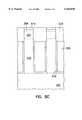
- FIG. 2is a plan view of an illustrative embodiment of a layout for a memory array according to the teachings of the present invention.
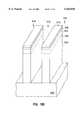
- FIG. 3is a perspective view of the illustrative embodiment of FIG. 2.
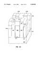
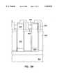
- FIG. 4is an elevational view of an illustrative embodiment of a memory cell with a body contact according to the teachings of the present invention.
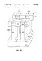
- FIGS. 5A through 5Oare perspective and elevational views of an embodiment of an integrated circuit that illustrate processing steps for fabricating the integrated circuit according to the teachings of the present invention.
- wafer and substrateare interchangeably used to refer generally to any structure on which integrated circuits are formed, and also to such structures during various stages of integrated circuit fabrication. Both terms include doped and undoped semiconductors, epitaxial layers of a semiconductor on a supporting semiconductor or insulating material, combinations of such layers, as well as other such structures that are known in the art.
- horizontalas used in this application is defined as a plane parallel to the conventional plane or surface of a wafer or substrate, regardless of the orientation of the wafer or substrate.
- verticalrefers to a direction perpendicular to the horizonal as defined above. Prepositions, such as “on”, “side” (as in “sidewall”), “higher”, “lower”, “over” and “under” are defined with respect to the conventional plane or surface being on the top surface of the wafer or substrate, regardless of the orientation of the wafer or substrate.
- FIG. 1is a block/schematic diagram that illustrates generally one embodiment of a memory device 100 incorporating an array of memory cells constructed according to the teachings of the present invention.
- Memory device 100is coupled to electronic system 101.
- Electronic system 101may comprise, for example, a microprocessor, a memory controller, a chip set or other appropriate electronic system.
- Memory device 100illustrates, by way of example but not by way of limitation, a dynamic random access memory (DRAM), in an open bit line configuration.
- Memory device 100includes memory arrays 110A and 110B. Each array includes N rows and M columns of memory cells 112-ij, where i refers to the row of the cell and j refers to the column of the cell.
- DRAMdynamic random access memory
- each of memory cells 112-ijhas a substantially identical structure, and accordingly, only one memory cell is described herein.
- These memory cells 112-ijinclude a vertical transistor where one plate of a capacitor is integral with the transistor.
- Memory cell 112-11includes vertical transistor 130-11.
- a source/drain region of transistor 130-11is formed in a deep trench and extends to a sufficient depth to form a storage node of storage capacitor 132-11.
- the other terminal of storage capacitor 132-11is part of a mesh or grid of poly-silicon that surrounds the source/drain region of transistor 130-11 and is coupled to ground potential.
- Each of the N rows of memory cellsincludes one of word lines WL-1 through WL-N that is formed in a trench separating adjacent rows of memory cells 112-ij. Portions of word lines WL-1 through WL-N adjacent to transistors 130-ij act as gate regions for the respective transistors.
- Each of the M columnsincludes one of bit lines BL-1 through BL-M.
- Bit lines BL-1 through BL-Mare used to write to and read data from memory cells 112-ij.
- Word lines WL-1 through WL-Nare used to access a particular row of memory cells 112-ij that is to be written or read.
- Addressing circuitryis also included.
- address buffer 114is coupled to control column decoder 118, which also includes sense amplifiers and input/output circuitry that is coupled to bit lines BL-1 through BL-M of arrays 110A and 110B.
- Address buffer 114also is coupled to control row decoders 116A and 116B. Row decoders 116A and B and column decoder 118 selectably access memory cells 112-ij in response to address signals that are provided on address lines 120 from electronic system 101 during write and read operations.
- Memory 100also includes body address line R-1 through R-N. As illustrated, the body address lines are coupled to word line decoder 116 so as to selectively control the potential applied to the body of the vertical transistors.
- the body address line and the word address linecan be driven with in a synchronous body address technique in which the body is driven slightly positive when the cell is addressed and slightly negative when not addressed.
- thisprovides more overdrive when the cell is addressed and less leakage when the cell is in standby. This also reduces the requirements on threshold voltage control of the access transistor. Any threshold voltage without body bias around zero volts is sufficient.
- memory 100receives an address of a particular memory cell at address buffer 114.
- electronic system 101may provide address buffer 114 with the address for cell 112-11 of array 110A.
- Address buffer 114identifies word line WL-1 for memory cell 112-11 to row decoder 116A.
- Row decoder 116Aselectively activates word line WL-1 to activate access transistor 130-1j of each memory cell 112-1j that is connected to word line WL-1.
- Column decoder 118selects bit lines BL-1 for memory cell 112-11.
- data received by input/output circuitryis coupled to bit lines BL-1 and through the access transistor 130-11 to charge or discharge storage capacitor 132-11 of memory cell 112-11 to represent binary data.
- bit line BL-1 of array 110Ais equilibrated with bit line BL-1 of array 110B.
- Data stored in memory cell 112-11, as represented by the charge on its storage capacitor 132-11,is coupled to bit line BL-1 of array 110A.
- the difference in charge in bit lines BL-1 of array 110A and bit line BL-1 of array 110Bis amplified, and a corresponding voltage level is provided to the input/output circuits.
- Body address linesare driven according to the synchronous technique described above.
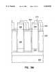
- FIGS. 2 through 4illustrate an embodiment of a memory cell with a vertical transistor and trench capacitor for use, for example, in memory device 100 of FIG. 1.
- FIG. 2is a plan view of a layout of a number of memory cells indicated generally at 202A through 202D in array 200.
- FIG. 2depicts only four memory cells. It is understood, however, that array 200 may include a larger number of memory cells even though only four are depicted here.
- Memory cell 202Dincludes pillar 204 of single crystal semiconductor material, e.g., silicon that is divided into first source/drain region 206, body region 208, and second source/drain region 210 to form access transistor 211. Pillar 204 extends vertically outward from substrate 213, for example, p- silicon. First source/drain region 206 and second source/drain region 210 each comprise, for example, n+ silicon and body region 208 comprises p- silicon.
- Word line 212passes body region 208 of access transistor 211 in isolation trench 214.
- Word line 212is separated from body region 208 of access transistor 204 by gate oxide 216 such that the portion of word line 212 adjacent to body region 208 operates as a gate for access transistor 211.
- Word line 212may comprise, for example, n+ poly-silicon material that is deposited in isolation trench 214 using a technique such that word line 212 is less than a minimum feature size, F, for the lithographic technique used to fabricate array 200.
- Cell 202Dis coupled in a column with cell 202A by bit line 218.
- Memory cell 202Dalso includes storage capacitor 219 for storing data in the cell.
- a first plate of capacitor 219 for memory cell 202Dis integral with second source/drain region 210 of access transistor 211.
- Second plate 220 of capacitor 219is common to all of the capacitors of array 200.
- Second plate 220comprises a mesh or grid of n+ poly-silicon formed in deep trenches that surrounds at least a portion of second source/drain region 210 of each pillar 204A through 204D.
- Second plate 220is grounded by contact with substrate 213 underneath the trenches.
- Second plate 220is separated from source/drain region 210 by gate oxide 222.
- the access transistors of memory array 200are also coupled to body address lines.
- FIG. 2depicts body address line 230 that is coupled to cells 202A and 202B.
- FIG. 4also illustrates that the body address line for a particular memory cell is located on a side opposite the word line for the cell.
- the memory cells of array 200are four-square feature (4F 2 ) memory cells.
- the surface area of cell 202Dis calculated based on linear dimensions in the bit line and word line directions. In the bit line direction, the distance from one edge of cell 202D to a common edge of adjacent cell 202A is approximately 2 minimum feature sizes (2F). In the word line direction, the dimension is taken from the midpoint of isolation trenches on either side of memory cell 202D. Again, this is approximately two minimum feature sizes (2F). Thus, the size of the cell is 4F 2 . This size is much smaller than the current cells with stacked capacitors or trench capacitors.
- FIGS. 5A through 5Oillustrate one embodiment of a process for fabricating an array of memory cells, indicated generally at 299, according to the teachings of the present invention.
- dimensionsare given that are appropriate to a 0.2 micrometer lithographic image size.
- the horizontal and vertical dimensionscan be scaled accordingly.
- Substrate 300comprises, for example, a P-type silicon wafer, layer of P- silicon material, or other appropriate substrate material.
- Layer 302is formed, for example, by epitaxial growth outwardly from layer 300.
- Layer 302comprises single crystalline N+ silicon that is approximately 3.5 micrometers thick.
- Layer 304is formed outwardly from layer 302 by epitaxial growth of single crystalline P- silicon of approximately 0.5 microns.
- Layer 306is formed by ion implantation of donor dopant into layer 304 such that layer 306 comprises single crystalline N+ silicon with a depth of approximately 0.1 microns.
- Pad oxide 308has a thickness of approximately 10 nanometers.
- Pad nitride 310has a thickness of approximately 200 nanometers.
- Photo resist layer 312is deposited outwardly from layer 310. Photo resist layer 312 is patterned with a mask to define openings 314 in layer 312 to be used in selective etching. As shown in FIG. 5B, column isolation trenches 316 are etched through openings 314 in photo resist layer 312 in a direction parallel to which the bit lines will be formed. Column isolation trenches 316 extend down through nitride layer 310, oxide layer 308, N+ layer 306, P- layer 304, N+ layer 302, and into substrate 300.
- a thin thermal protective oxide layer 318is grown on exposed surfaces of substrate 300 and layers 302, 304, and 306. Layer 318 is used to protect substrate 300 and layers 302, 304 and 306 during subsequent process step.
- a layer of intrinsic poly-silicon 320is deposited by chemical vapor deposition (CVD) to fill column isolation trenches 316.
- Layer 320is etched by reactive ion etching (RIE) such that layer 320 is recessed below a top of layer 302.
- RIEreactive ion etching
- Layer 322 of silicon nitride (Si 3 N 4 )is deposited by, for example, chemical vapor deposition to fill trenches 316.
- Layer 322is planarized back to a level of layer 310 using, for example, chemical mechanical polishing (CMP) or other suitable planarization technique to produce the structure shown in FIG. 5C.
- CMPchemical mechanical polishing
- layer 324 of photo resist materialis deposited outwardly from nitride layers 322 and 310.
- Layer 324is exposed through a mask to define openings 326 in layer 324. Openings 326 are orthogonal to trenches 316 that were filled by intrinsic poly-silicon layer 320 and nitride layer 322.
- nitride layers 310 and 322are etched to a depth sufficient to expose a working surface 328 of layer 306. It is noted that at this point layer 320 of intrinsic poly-silicon is still covered by a portion of nitride layer 322.
- the portion of layers 306, 304, and 302 that are exposed in openings 326are selectively etched down to a distance approximately equal to column isolation trenches 316.
- the remaining nitride layer 322 exposed in openings 326is directionally etched to expose layer of intrinsic poly-silicon 320. It is noted that nitride layer 322 and nitride layer 310 remain intact under the photo resist layer 324. Layer 324 is removed.
- Thermal oxide layer 330is formed by, for example, growing a 20 nanometer layer of oxide on exposed silicon and intrinsic poly-silicon in openings 326. Intrinsic poly-silicon is deposited through openings 326 to refill the trenches. The intrinsic poly-silicon in openings 326 is directionally etched, selective to nitride. A brief oxide etch is used to clear oxide layer 330 from intrinsic poly-silicon 320. The intrinsic poly-silicon in openings 326 is etched to the same depth as trenches 316 so as to form row isolation trenches 332. The structure is now as shown in FIG. 5G.
- Nitrideis deposited by chemical vapor deposition in trenches 332 to a thickness of approximately 20 nanometers.
- the nitrideis directionally etched to leave on the vertical sidewalls of trenches 332.
- an isotropic oxide etchis used to remove all exposed thin oxide, clearing oxide from the bottom of trenches 332.
- Thermal oxide layer 333is formed beneath single crystal silicon pillars 334A through 334D. This is accomplished by first doing an isotropic silicon etch that etches both single crystal and intrinsic poly-silicon downward and laterally to completely undercut pillars 334A through 334D. Although completely undercut, pillars 334A through 334D are supported by contact with original crystal at the ends. Next, thermal oxide layer 333 is grown with a thickness of approximately 0.1 micrometers (for 0.2 micrometer CD) beneath pillars 334A through 334D. The nitride is removed from the sidewalls of trenches 332 to expose the remaining intrinsic poly-silicon of layer 320. It is noted that pillars 334A through 334D are still covered with protective oxide 330. At this point the structure is as shown in FIG. 5H.
- the remaining portions of intrinsic poly-siliconare removed by an isotropic etch. Further, all exposed thin thermal oxide is removed from the walls of pillars 334A through 334D with an isotropic etch leaving the structure shown in FIG. 5I.
- This structureincludes nitride bridges 335 formed from nitride layers 310 and 322 that extend orthogonal to column isolation trenches 316 and cover the remaining portions of layers 302, 304, and 306.
- the structurealso includes row isolation trenches 332 that are orthogonal to column isolation trenches 316.
- the structure of FIG. 5Ialso includes pillars 334A through 334D of single crystal silicon material. Pillars 334A through 334D form the basis for individual memory cells for the memory array formed by the process.
- Conductor mesh or grid 340is formed in trenches 332 and 316. Exposed oxide layer 333 in trenches 332 is directionally etched down to expose underlying layer 300 in trenches 332.
- a refractory metale.g., Ti, W, is deposited by collimated deposition onto the exposed surface of layer 300 to form metal contact 331.
- insulator layer 338is formed by depositing an insulator material in trenches 316 and 332. Layer 338 is used as the insulator layer for the storage capacitors in array 299. In embodiments involving metal contact 331, layer 338 is directionally etched to remove layer 338 from the bottom of trenches 332 to expose metal contact 331.
- a common plate for all of the memory cells of array 299is formed by a chemical vapor deposition of N+ poly-silicon or other appropriate refractory conductor in column isolation trenches 316 and row isolation trenches 332. In this manner, conductor mesh or grid 340 is formed so as to surround each of pillars 334A through 334D.
- Mesh 340is planarized and etched back to a level approximately at the bottom of bridges 335 as shown in FIG. 5J. An additional etch is performed to remove any remaining exposed insulator material of layer 338 from the sides of semiconductor pillars 334A through 334D above mesh 340.
- Nitrideis deposited by, for example, chemical vapor deposition into channels 332 to a thickness of approximately 20 nanometers. The nitride is directionally etched to leave on sidewalls 350 of pillars 334A through 334D.
- Thermal oxide cap 352is formed by, for example, growing a layer of oxide on exposed portions of poly-silicon mesh 340 in trenches 332. The nitride is stripped from sidewalls 350 of pillars 334A through 334D.
- gate oxide 354is formed on surface 350 of pillars 334A through 334D.
- a layer of n+ poly-siliconis deposited in trenches 332 to a thickness of approximately one-third of the critical dimension of the processing technique.
- the n+ poly-siliconis directionally etched to leave as word lines 356 on one side of pillars 334A through 334D.
- the n+ poly-siliconforms spacers that will be replaced with body contacts in subsequent processing steps. It is noted that the portions of word lines 356 that are disposed adjacent to pillars 334A through 334D act as gates for the access transistors of array 299.
- nitride layer 358is formed by, for example, chemical vapor deposition of nitride so as to fill trenches 358 and cover array 299.
- Nitride layer 358is planarized, e.g., using a chemical/mechanical polishing technique.
- Photo resist layeris deposited and exposed through a mask to define stripes in layer 360 that expose approximately half of each trench 332 that contains spacers 357. This leaves the structure as shown in FIG. 5L.
- Nitride layer 358is directionally etched through openings 362 in photoresist layer 360 to a depth sufficient to expose the top of poly-silicon spacers 357. It is noted that a portion of layer 310 may also be removed. Poly-silicon spacers 357 are etched so as to remove the spacers. Gate oxide layer 354 is isotropically etched so as to remove the gate oxide from exposed sidewall 350 of pillars 334A through 334D. Photo resist layer 360 is removed. Oxide layer 364 is deposited, by for example, chemical vapor deposition to fill the space vacated by spacers 357. Oxide layer 364 is planarized using, for example, a chemical/mechanical polishing technique to planarize with the surface of the nitride. Oxide layer 364 is further etched to a depth sufficient to expose p- silicon in layer 304 as shown in FIG. 5M.
- P+ poly-siliconis deposited by, for example, chemical vapor deposition to fill the space vacated by oxide layer 364.
- the p+ poly-siliconis planarized with the surface of the nitride.
- the p+ poly-silicon materialis etched to below the top of layer 304 to form body contacts 366 for array 299 as shown in FIG. 5N.
- Oxideis deposited to fill and is planarized to be level with a top surface of the nitride.
- the remaining exposed nitrideis stripped with an isotropic etch.
- the exposed word lines 358are etched to recess the word lines below the top surface of pillars 334A through 334C. This produces the final structure as shown in FIG. 5O with transistors 368A through 368D and bit lines 370.
Landscapes
- Engineering & Computer Science (AREA)
- Manufacturing & Machinery (AREA)
- Semiconductor Memories (AREA)
Abstract
Description
This application is a divisional of U.S. Ser. No. 08/939,732 now U.S. Pat. No. 5,907,170 filed Oct. 6, 1997.
The present invention relates generally to the field of memory devices and, in particular, to a circuit and method for an open bit line memory cell with a vertical transistor and trench plate trench capacitor
Electronic systems typically store data during operation in a memory device. In recent years, the dynamic random access memory (DRAM) has become a popular data storage device for such systems. Basically, a DRAM is an integrated circuit that stores data in binary form (e.g., "1" or "0") in a large number of cells. The data is stored in a cell as a charge on a capacitor located within the cell. Typically, a high logic level is approximately equal to the power supply voltage and a low logic level is approximately equal to ground.
The cells of a conventional DRAM are arranged in an array so that individual cells can be addressed and accessed. The array can be thought of as rows and columns of cells. Each row includes a word line that interconnects cells on the row with a common control signal. Similarly, each column includes a bit line that is coupled to at most one cell in each row. Thus, the word and bit lines can be controlled so as to individually access each cell of the array.
A memory array is typically implemented as an integrated circuit on a semiconductor substrate in one of a number of conventional layouts. One such layout is referred to as an "open digit line" architecture. In this architecture, the array is divided into at least two separate parts or "sub-arrays." Each sub-array includes a number of rows and columns of memory cells. Each memory cell in a row is coupled to a common word line and each transistor in a column is coupled to a common bit line. Each bit line in the first sub-array is paired with a bit line in the second sub-array so as to feed into a common sense amplifier. The sense amplifier detects and amplifies differences in voltage on a pair of bit lines as described in more detail below.
To read data out of a cell, the capacitor of a cell is accessed by selecting the word line associated with the cell. A complementary bit line that is paired with the bit line for the selected cell is equilibrated with the voltage on the bit line for the selected cell. The equilibration voltage is typically midway between the high and low logic levels. Thus, conventionally, the bit lines are equilibrated to one-half of the power supply voltage, VCC /2. When the word line is activated for the selected cell, the capacitor of the selected cell discharges the stored voltage onto the bit line, thus changing the voltage on the bit line.
The sense amplifier detects and amplifies the difference in voltage on the pair of bit lines. The sense amplifier typically includes two main components: an n-sense amplifier and a p-sense amplifier. The n-sense amplifier includes a cross-coupled pair of n-channel transistors that drive the low bit line to ground. The p-sense amplifier includes a cross-coupled pair of p-channel transistors and is used to drive the high bit line to the power supply voltage.
An input/output device for the array, typically an n-channel transistor, passes the voltage on the bit line for the selected cell to an input/output line for communication to, for example, a processor of a computer or other electronic system associated with the DRAM. In a write operation, data is passed from the input/output lines to the bit lines by the input/output device of the array for storage on the capacitor in the selected cell.
Each of the components of a memory device are conventionally formed as part of an integrated circuit on a "chip" or wafer of semiconductor material. One of the limiting factors in increasing the capacity of a memory device is the amount of surface area of chip used to form each memory cell. In the industry terminology, the surface area required for a memory cell is characterized in terms of the minimum feature size, "F," that is obtainable by the lithography technology used to form the memory cell. Conventionally, the memory cell is laid out with a transistor that includes first and second source/drain regions separated by a body or gate region that are disposed horizontally along a surface of the chip. When isolation between adjacent transistors is considered, the surface area required for such a transistor is generally 8F2 or 6F2.
Some researchers have proposed using a vertical transistor in the memory cell in order to reduce the surface area of the chip required for the cell. Each of these proposed memory cells, although smaller in size from conventional cells, fails to provide adequate operational characteristics when compared to more conventional structures. For example, U.S. Pat. No. 4,673,962 (the '962 Patent) issued to Texas Instruments on Jun. 16, 1997. The '962 Patent discloses the use of a thin poly-silicon field effect transistor (FET) in a memory cell. The poly-silicon FET is formed along a sidewall of a trench which runs vertically into a substrate. At a minimum, the poly-silicon FET includes a junction between poly-silicon channel (58) and the bit line (20) as shown in FIG. 3 of the '962 Patent. Unfortunately, this junction is prone to charge leakage and thus the poly-silicon FET may have inadequate operational qualities to control the charge on the storage capacitor. Other known disadvantages of such thin film poly-silicon devices may also hamper the operation of the proposed cell.
Other researchers have proposed use of a "surrounding gate transistor" in which a gate or word line completely surrounds a vertical transistor. See, e.g., Impact of a Vertical Φ-shape transistor (VΦT) Cell for 1 Gbit DRAM and Beyond, IEEE Trans. On Elec. Devices, Vol 42, No.12, December, 1995, pp. 2117-2123. Unfortunately, these devices suffer from problems with access speed due to high gate capacitance caused by the increased surface area of the gate which slows down the rise time of the word lines. Other vertical transistor cells include a contact between the pass transistor and a poly-silicon plate in the trench. Such vertical transistor cells are difficult to implement due to the contact and should produce a low yield.
For the reasons stated above, and for other reasons stated below which will become apparent to those skilled in the art upon reading and understanding the present specification, there is a need in the art for realizable memory cell that uses less surface area than conventional memory cells.
The above mentioned problems with memory cells and other problems are addressed by the present invention and which will be understood by reading and studying the following specification. A memory cell is described which includes a vertical transistor with a trench plate trench capacitor and a body contact.
In particular, one embodiment of the present invention provides a memory cell. The memory cell includes an access transistor. The access transistor is formed in a pillar of single crystal semiconductor material. The transistor has first and second source/drain regions and a body region that are vertically aligned. The memory cell also includes a body contact that is coupled to the body region. A gate of the transistor is disposed on a side of the pillar that is opposite from the body contact. A trench capacitor is also included. The trench capacitor includes a first plate that is formed integral with the first source/drain region of the access transistor and a second plate that is disposed adjacent to the first plate and separated from the first plate by a gate oxide. An insulator layer separates the access transistor and the trench capacitor from an underlying layer of semiconductor material.
In another embodiment, a memory device is provided. The memory device includes an array of memory cells. Each cell includes a vertical access transistor formed of a semiconductor pillar that extends outwardly from an insulator layer on a substrate. The access transistor has body and first and second source/drain regions, a gate disposed adjacent to a side of the pillar adjacent to the body region, and a trench capacitor. The first plate of the trench capacitor is integral with the first source/drain region and a second plate of the capacitor is disposed adjacent to the first plate. A number of bit lines are each selectively coupled to a number of the memory cells at the second source/drain region of the access transistor so as to form columns of memory cells. A number of word lines are also provided. Each word line is disposed orthogonally to the bit lines in a trench between rows of the memory cells for addressing gates of the access transistors of the memory cells that are adjacent to the word line. A number of body lines is also provided. Each body line is disposed in a trench between rows of memory cells so as to contact the body regions of access transistors on a side of the trench opposite the word line in the trench. Further the memory device includes a row decoder that is coupled to the word lines and body lines and a column decoder that is coupled to the bit lines so as to selectively access the cells of the array.
In another embodiment, a memory array is provided. The memory array includes an array of memory cells. Each memory cell includes an access transistor. The access transistor has body and first and second source/drain regions that are vertically formed outwardly from an insulator layer on a substrate in a single crystalline semiconductor pillar and a gate that is disposed adjacent to a side of the transistor. The second source/drain region includes an upper semiconductor surface. A number of word lines are included that interconnect gates of selected access transistors so as to form a number of rows of memory cells. A number of body address lines also interconnect body regions of selected access transistors in the rows of memory cells. A number of first isolation trenches separate adjacent rows of memory cells. Each isolation trench houses a word line and a body address line. A number of second isolation trenches are also provided. Each second isolation trench is substantially orthogonal to the first isolation trenches and interposed between adjacent memory cells so as to form a number of columns of the array.
In another embodiment, a method of fabricating a memory array is provided. A number of access transistors are formed. Each access transistor is formed in a pillar of semiconductor material that extends outwardly from a substrate. The access transistor includes a first source/drain region, a body region and a second source/drain region formed vertically thereupon. A trench capacitor for each access transistor is also formed. A first plate of the trench capacitor is integral with the first source/drain region of the access transistor. A number of word lines interconnect the gates of a number of access transistors to form a row of the array. The word lines are disposed in a number of trenches that separate adjacent rows of access transistors. A number of body address lines that interconnect body regions of access transistors along the rows of the array are also formed. A number of bit lines that interconnect second source/drain regions of selected access transistors are formed so as to form a number of columns of the array.
FIG. 1 is a block/schematic diagram of an illustrative embodiment of the present invention that includes a memory device that is coupled to an electronic system.
FIG. 2 is a plan view of an illustrative embodiment of a layout for a memory array according to the teachings of the present invention.
FIG. 3 is a perspective view of the illustrative embodiment of FIG. 2.
FIG. 4 is an elevational view of an illustrative embodiment of a memory cell with a body contact according to the teachings of the present invention.
FIGS. 5A through 5O are perspective and elevational views of an embodiment of an integrated circuit that illustrate processing steps for fabricating the integrated circuit according to the teachings of the present invention.
In the following detailed description of the invention, reference is made to the accompanying drawings which form a part hereof, and in which is shown, by way of illustration, specific embodiments in which the invention may be practiced. The embodiments are intended to describe aspects of the invention in sufficient detail to enable those skilled in the art to practice the invention. Other embodiments may be utilized and logical, mechanical and electrical changes may be made without departing from the scope of the present invention. The following detailed description is, therefore, not to be taken in; a limiting sense.
In the following description, the terms wafer and substrate are interchangeably used to refer generally to any structure on which integrated circuits are formed, and also to such structures during various stages of integrated circuit fabrication. Both terms include doped and undoped semiconductors, epitaxial layers of a semiconductor on a supporting semiconductor or insulating material, combinations of such layers, as well as other such structures that are known in the art.
The term "horizontal" as used in this application is defined as a plane parallel to the conventional plane or surface of a wafer or substrate, regardless of the orientation of the wafer or substrate. The term "vertical" refers to a direction perpendicular to the horizonal as defined above. Prepositions, such as "on", "side" (as in "sidewall"), "higher", "lower", "over" and "under" are defined with respect to the conventional plane or surface being on the top surface of the wafer or substrate, regardless of the orientation of the wafer or substrate.
FIG. 1 is a block/schematic diagram that illustrates generally one embodiment of amemory device 100 incorporating an array of memory cells constructed according to the teachings of the present invention.Memory device 100 is coupled toelectronic system 101.Electronic system 101 may comprise, for example, a microprocessor, a memory controller, a chip set or other appropriate electronic system.Memory device 100 illustrates, by way of example but not by way of limitation, a dynamic random access memory (DRAM), in an open bit line configuration.Memory device 100 includesmemory arrays
In the exemplary embodiment of FIG. 1, each of memory cells 112-ij has a substantially identical structure, and accordingly, only one memory cell is described herein. These memory cells 112-ij include a vertical transistor where one plate of a capacitor is integral with the transistor. Memory cell 112-11 includes vertical transistor 130-11. A source/drain region of transistor 130-11 is formed in a deep trench and extends to a sufficient depth to form a storage node of storage capacitor 132-11. The other terminal of storage capacitor 132-11 is part of a mesh or grid of poly-silicon that surrounds the source/drain region of transistor 130-11 and is coupled to ground potential.
Each of the N rows of memory cells includes one of word lines WL-1 through WL-N that is formed in a trench separating adjacent rows of memory cells 112-ij. Portions of word lines WL-1 through WL-N adjacent to transistors 130-ij act as gate regions for the respective transistors. Each of the M columns includes one of bit lines BL-1 through BL-M.
Bit lines BL-1 through BL-M are used to write to and read data from memory cells 112-ij. Word lines WL-1 through WL-N are used to access a particular row of memory cells 112-ij that is to be written or read. Addressing circuitry is also included. For example,address buffer 114 is coupled to controlcolumn decoder 118, which also includes sense amplifiers and input/output circuitry that is coupled to bit lines BL-1 through BL-M ofarrays Address buffer 114 also is coupled to controlrow decoders Row decoders 116A and B andcolumn decoder 118 selectably access memory cells 112-ij in response to address signals that are provided onaddress lines 120 fromelectronic system 101 during write and read operations.
In operation,memory 100 receives an address of a particular memory cell ataddress buffer 114. For example,electronic system 101 may provideaddress buffer 114 with the address for cell 112-11 ofarray 110A.Address buffer 114 identifies word line WL-1 for memory cell 112-11 to rowdecoder 116A.Row decoder 116A selectively activates word line WL-1 to activate access transistor 130-1j of each memory cell 112-1j that is connected to word line WL-1.Column decoder 118 selects bit lines BL-1 for memory cell 112-11. For a write operation, data received by input/output circuitry is coupled to bit lines BL-1 and through the access transistor 130-11 to charge or discharge storage capacitor 132-11 of memory cell 112-11 to represent binary data. For a read operation, bit line BL-1 ofarray 110A is equilibrated with bit line BL-1 ofarray 110B. Data stored in memory cell 112-11, as represented by the charge on its storage capacitor 132-11, is coupled to bit line BL-1 ofarray 110A. The difference in charge in bit lines BL-1 ofarray 110A and bit line BL-1 ofarray 110B is amplified, and a corresponding voltage level is provided to the input/output circuits. Body address lines are driven according to the synchronous technique described above.
FIGS. 2 through 4 illustrate an embodiment of a memory cell with a vertical transistor and trench capacitor for use, for example, inmemory device 100 of FIG. 1. Specifically, FIG. 2 is a plan view of a layout of a number of memory cells indicated generally at 202A through 202D inarray 200. FIG. 2 depicts only four memory cells. It is understood, however, thatarray 200 may include a larger number of memory cells even though only four are depicted here.
Each memory cell is constructed in a similar manner. Thus, onlymemory cell 202D in FIG. 3 is described herein in detail.Memory cell 202D includespillar 204 of single crystal semiconductor material, e.g., silicon that is divided into first source/drain region 206,body region 208, and second source/drain region 210 to formaccess transistor 211.Pillar 204 extends vertically outward fromsubstrate 213, for example, p- silicon. First source/drain region 206 and second source/drain region 210 each comprise, for example, n+ silicon andbody region 208 comprises p- silicon.
The access transistors ofmemory array 200 are also coupled to body address lines. For example, FIG. 2 depictsbody address line 230 that is coupled tocells
As shown in FIG. 2, the memory cells ofarray 200 are four-square feature (4F2) memory cells. Usingcell 202D as an example, the surface area ofcell 202D is calculated based on linear dimensions in the bit line and word line directions. In the bit line direction, the distance from one edge ofcell 202D to a common edge ofadjacent cell 202A is approximately 2 minimum feature sizes (2F). In the word line direction, the dimension is taken from the midpoint of isolation trenches on either side ofmemory cell 202D. Again, this is approximately two minimum feature sizes (2F). Thus, the size of the cell is 4F2. This size is much smaller than the current cells with stacked capacitors or trench capacitors.
FIGS. 5A through 5O illustrate one embodiment of a process for fabricating an array of memory cells, indicated generally at 299, according to the teachings of the present invention. In this example, dimensions are given that are appropriate to a 0.2 micrometer lithographic image size. For other image sizes, the horizontal and vertical dimensions can be scaled accordingly.
As shown in FIG. 5A, the method begins withsubstrate 300.Substrate 300 comprises, for example, a P-type silicon wafer, layer of P- silicon material, or other appropriate substrate material.Layer 302 is formed, for example, by epitaxial growth outwardly fromlayer 300.Layer 302 comprises single crystalline N+ silicon that is approximately 3.5 micrometers thick.Layer 304 is formed outwardly fromlayer 302 by epitaxial growth of single crystalline P- silicon of approximately 0.5 microns.Layer 306 is formed by ion implantation of donor dopant intolayer 304 such thatlayer 306 comprises single crystalline N+ silicon with a depth of approximately 0.1 microns.
A thin layer of silicon dioxide (SiO2), referred to aspad oxide 308, is deposited or grown onlayer 306.Pad oxide 308 has a thickness of approximately 10 nanometers. A layer of silicon nitride (Si3 N4), referred to aspad nitride 310, is deposited onpad oxide 308.Pad nitride 310 has a thickness of approximately 200 nanometers.
Photo resistlayer 312 is deposited outwardly fromlayer 310. Photo resistlayer 312 is patterned with a mask to defineopenings 314 inlayer 312 to be used in selective etching. As shown in FIG. 5B,column isolation trenches 316 are etched throughopenings 314 in photo resistlayer 312 in a direction parallel to which the bit lines will be formed.Column isolation trenches 316 extend down throughnitride layer 310,oxide layer 308,N+ layer 306, P-layer 304,N+ layer 302, and intosubstrate 300.
A thin thermalprotective oxide layer 318 is grown on exposed surfaces ofsubstrate 300 andlayers Layer 318 is used to protectsubstrate 300 andlayers
A layer of intrinsic poly-silicon 320 is deposited by chemical vapor deposition (CVD) to fillcolumn isolation trenches 316.Layer 320 is etched by reactive ion etching (RIE) such thatlayer 320 is recessed below a top oflayer 302.Layer 322 of silicon nitride (Si3 N4) is deposited by, for example, chemical vapor deposition to filltrenches 316.Layer 322 is planarized back to a level oflayer 310 using, for example, chemical mechanical polishing (CMP) or other suitable planarization technique to produce the structure shown in FIG. 5C.
As shown in FIG. 5D,layer 324 of photo resist material is deposited outwardly fromnitride layers Layer 324 is exposed through a mask to defineopenings 326 inlayer 324.Openings 326 are orthogonal totrenches 316 that were filled by intrinsic poly-silicon layer 320 andnitride layer 322. Next, nitride layers 310 and 322 are etched to a depth sufficient to expose a workingsurface 328 oflayer 306. It is noted that at thispoint layer 320 of intrinsic poly-silicon is still covered by a portion ofnitride layer 322.
As shown in FIG. 5E, the portion oflayers openings 326 are selectively etched down to a distance approximately equal tocolumn isolation trenches 316.
As shown in FIG. 5F, the remainingnitride layer 322 exposed inopenings 326 is directionally etched to expose layer of intrinsic poly-silicon 320. It is noted thatnitride layer 322 andnitride layer 310 remain intact under the photo resistlayer 324.Layer 324 is removed.Thermal oxide layer 330 is formed by, for example, growing a 20 nanometer layer of oxide on exposed silicon and intrinsic poly-silicon inopenings 326. Intrinsic poly-silicon is deposited throughopenings 326 to refill the trenches. The intrinsic poly-silicon inopenings 326 is directionally etched, selective to nitride. A brief oxide etch is used toclear oxide layer 330 from intrinsic poly-silicon 320. The intrinsic poly-silicon inopenings 326 is etched to the same depth astrenches 316 so as to formrow isolation trenches 332. The structure is now as shown in FIG. 5G.
Nitride is deposited by chemical vapor deposition intrenches 332 to a thickness of approximately 20 nanometers. The nitride is directionally etched to leave on the vertical sidewalls oftrenches 332. Next, an isotropic oxide etch is used to remove all exposed thin oxide, clearing oxide from the bottom oftrenches 332.
The remaining portions of intrinsic poly-silicon are removed by an isotropic etch. Further, all exposed thin thermal oxide is removed from the walls ofpillars 334A through 334D with an isotropic etch leaving the structure shown in FIG. 5I. This structure includes nitride bridges 335 formed fromnitride layers column isolation trenches 316 and cover the remaining portions oflayers row isolation trenches 332 that are orthogonal tocolumn isolation trenches 316. The structure of FIG. 5I also includespillars 334A through 334D of single crystal silicon material.Pillars 334A through 334D form the basis for individual memory cells for the memory array formed by the process.
Conductor mesh orgrid 340 is formed intrenches Exposed oxide layer 333 intrenches 332 is directionally etched down to exposeunderlying layer 300 intrenches 332. A refractory metal, e.g., Ti, W, is deposited by collimated deposition onto the exposed surface oflayer 300 to formmetal contact 331.
Next,insulator layer 338 is formed by depositing an insulator material intrenches Layer 338 is used as the insulator layer for the storage capacitors inarray 299. In embodiments involvingmetal contact 331,layer 338 is directionally etched to removelayer 338 from the bottom oftrenches 332 to exposemetal contact 331. A common plate for all of the memory cells ofarray 299 is formed by a chemical vapor deposition of N+ poly-silicon or other appropriate refractory conductor incolumn isolation trenches 316 and rowisolation trenches 332. In this manner, conductor mesh orgrid 340 is formed so as to surround each ofpillars 334A through 334D.Mesh 340 is planarized and etched back to a level approximately at the bottom ofbridges 335 as shown in FIG. 5J. An additional etch is performed to remove any remaining exposed insulator material oflayer 338 from the sides ofsemiconductor pillars 334A through 334D abovemesh 340.
Nitride is deposited by, for example, chemical vapor deposition intochannels 332 to a thickness of approximately 20 nanometers. The nitride is directionally etched to leave onsidewalls 350 ofpillars 334A through 334D.Thermal oxide cap 352 is formed by, for example, growing a layer of oxide on exposed portions of poly-silicon mesh 340 intrenches 332. The nitride is stripped fromsidewalls 350 ofpillars 334A through 334D.
As shown in FIG. 5K,gate oxide 354 is formed onsurface 350 ofpillars 334A through 334D. A layer of n+ poly-silicon is deposited intrenches 332 to a thickness of approximately one-third of the critical dimension of the processing technique. The n+ poly-silicon is directionally etched to leave as word lines 356 on one side ofpillars 334A through 334D. On the opposite side ofpillars 334A through 334D, the n+ poly-silicon forms spacers that will be replaced with body contacts in subsequent processing steps. It is noted that the portions ofword lines 356 that are disposed adjacent topillars 334A through 334D act as gates for the access transistors ofarray 299.
As shown in FIG. 5L,nitride layer 358 is formed by, for example, chemical vapor deposition of nitride so as to filltrenches 358 andcover array 299.Nitride layer 358 is planarized, e.g., using a chemical/mechanical polishing technique. Photo resist layer is deposited and exposed through a mask to define stripes inlayer 360 that expose approximately half of eachtrench 332 that containsspacers 357. This leaves the structure as shown in FIG. 5L.
P+ poly-silicon is deposited by, for example, chemical vapor deposition to fill the space vacated byoxide layer 364. The p+ poly-silicon is planarized with the surface of the nitride. The p+ poly-silicon material is etched to below the top oflayer 304 to formbody contacts 366 forarray 299 as shown in FIG. 5N.
Oxide is deposited to fill and is planarized to be level with a top surface of the nitride. The remaining exposed nitride is stripped with an isotropic etch. The exposedword lines 358 are etched to recess the word lines below the top surface ofpillars 334A through 334C. This produces the final structure as shown in FIG. 5O withtransistors 368A through 368D and bitlines 370.
Although specific embodiments have been illustrated and described herein, it will be appreciated by those of ordinary skill in the art that any arrangement which is calculated to achieve the same purpose may be substituted for the specific embodiment shown. This application is intended to cover any adaptations or variations of the present invention. For example, the semiconductor materials specified in this application are given by way of example and not by way of limitation. Other appropriate materials can be substituted without departing from the spirit and scope of the invention.
Claims (4)
1. A method of fabricating a memory array, the method comprising the steps of:
forming a number of access transistors, each access transistor formed in a pillar of semiconductor material that extends outwardly from a substrate wherein the access transistor includes a first source/drain region, a body region and a second source/drain region formed vertically thereupon;
forming a trench capacitor for each access transistor, wherein a first plate of the trench capacitor is integral with the first source/drain region of the access transistor;
forming a number of word lines that interconnect the gates of a number of access transistors to form a row of the array, the word lines disposed in a number of trenches that separate adjacent rows of access transistors;
forming a number of body address lines that interconnect body regions of access transistors along the rows of the array; and
forming a number of bit lines that interconnect second source/drain regions of selected access transistors so as to form a number of columns of the array.
2. The method of claim 1, wherein the step of forming a trench capacitor further includes the step of forming a second plate that surrounds the first plate.
3. The method of claim 1, and further comprising the step of forming a contact that couples a second plate of the trench capacitor to an underlying semiconductor layer.
4. The method of claim 1, where the step of forming a trench capacitor comprises the step of forming a second plate that forms a grid pattern in a layer of semiconductor material such that the grid surrounds each of the pillars that form the access transistors.
Priority Applications (2)
| Application Number | Priority Date | Filing Date | Title |
|---|---|---|---|
| US09/138,794US6165836A (en) | 1997-10-06 | 1998-08-24 | Circuit and method for an open bit line memory cell with a vertical transistor and trench plate trench capacitor |
| US09/742,568US6537871B2 (en) | 1997-10-06 | 2000-12-20 | Circuit and method for an open bit line memory cell with a vertical transistor and trench plate trench capacitor |
Applications Claiming Priority (2)
| Application Number | Priority Date | Filing Date | Title |
|---|---|---|---|
| US08/939,732US5907170A (en) | 1997-10-06 | 1997-10-06 | Circuit and method for an open bit line memory cell with a vertical transistor and trench plate trench capacitor |
| US09/138,794US6165836A (en) | 1997-10-06 | 1998-08-24 | Circuit and method for an open bit line memory cell with a vertical transistor and trench plate trench capacitor |
Related Parent Applications (1)
| Application Number | Title | Priority Date | Filing Date |
|---|---|---|---|
| US08/939,732DivisionUS5907170A (en) | 1997-10-06 | 1997-10-06 | Circuit and method for an open bit line memory cell with a vertical transistor and trench plate trench capacitor |
Related Child Applications (1)
| Application Number | Title | Priority Date | Filing Date |
|---|---|---|---|
| US09/742,568ContinuationUS6537871B2 (en) | 1997-10-06 | 2000-12-20 | Circuit and method for an open bit line memory cell with a vertical transistor and trench plate trench capacitor |
Publications (1)
| Publication Number | Publication Date |
|---|---|
| US6165836Atrue US6165836A (en) | 2000-12-26 |
Family
ID=25473622
Family Applications (3)
| Application Number | Title | Priority Date | Filing Date |
|---|---|---|---|
| US08/939,732Expired - LifetimeUS5907170A (en) | 1997-10-06 | 1997-10-06 | Circuit and method for an open bit line memory cell with a vertical transistor and trench plate trench capacitor |
| US09/138,794Expired - Fee RelatedUS6165836A (en) | 1997-10-06 | 1998-08-24 | Circuit and method for an open bit line memory cell with a vertical transistor and trench plate trench capacitor |
| US09/742,568Expired - LifetimeUS6537871B2 (en) | 1997-10-06 | 2000-12-20 | Circuit and method for an open bit line memory cell with a vertical transistor and trench plate trench capacitor |
Family Applications Before (1)
| Application Number | Title | Priority Date | Filing Date |
|---|---|---|---|
| US08/939,732Expired - LifetimeUS5907170A (en) | 1997-10-06 | 1997-10-06 | Circuit and method for an open bit line memory cell with a vertical transistor and trench plate trench capacitor |
Family Applications After (1)
| Application Number | Title | Priority Date | Filing Date |
|---|---|---|---|
| US09/742,568Expired - LifetimeUS6537871B2 (en) | 1997-10-06 | 2000-12-20 | Circuit and method for an open bit line memory cell with a vertical transistor and trench plate trench capacitor |
Country Status (1)
| Country | Link |
|---|---|
| US (3) | US5907170A (en) |
Cited By (17)
| Publication number | Priority date | Publication date | Assignee | Title |
|---|---|---|---|---|
| US6437383B1 (en)* | 2000-12-21 | 2002-08-20 | Intel Corporation | Dual trench isolation for a phase-change memory cell and method of making same |
| US6476434B1 (en) | 1997-07-08 | 2002-11-05 | Micron Tecnology, Inc. | 4 F2 folded bit line dram cell structure having buried bit and word lines |
| US6486703B2 (en) | 1998-08-04 | 2002-11-26 | Micron Technology, Inc. | Programmable logic array with vertical transistors |
| US6498065B1 (en) | 1998-08-04 | 2002-12-24 | Micron Technology, Inc. | Memory address decode array with vertical transistors |
| US6528837B2 (en) | 1997-10-06 | 2003-03-04 | Micron Technology, Inc. | Circuit and method for an open bit line memory cell with a vertical transistor and trench plate trench capacitor |
| US6534781B2 (en) | 2000-12-26 | 2003-03-18 | Ovonyx, Inc. | Phase-change memory bipolar array utilizing a single shallow trench isolation for creating an individual active area region for two memory array elements and one bipolar base contact |
| US6537871B2 (en)* | 1997-10-06 | 2003-03-25 | Micron Technology, Inc. | Circuit and method for an open bit line memory cell with a vertical transistor and trench plate trench capacitor |
| US6556068B2 (en) | 1998-02-26 | 2003-04-29 | Micron Technology, Inc. | Threshold voltage compensation circuits for low voltage and low power CMOS integrated circuits |
| US6566219B2 (en)* | 2000-09-22 | 2003-05-20 | Infineon Technologies Ag | Method of forming a self aligned trench in a semiconductor using a patterned sacrificial layer for defining the trench opening |
| US6764901B2 (en) | 1997-10-06 | 2004-07-20 | Micron Technology, Inc. | Circuit and method for a folded bit line memory cell with vertical transistor and trench capacitor |
| US6777744B2 (en) | 1998-02-24 | 2004-08-17 | Micron Technology, Inc. | Circuits and methods using vertical, complementary transistors |
| US6812516B2 (en) | 1998-02-27 | 2004-11-02 | Micron Technology, Inc. | Field programmable logic arrays with vertical transistors |
| US7005346B2 (en) | 2001-11-22 | 2006-02-28 | Infineon Technologies Ag | Method for producing a memory cell of a memory cell field in a semiconductor memory |
| US7049196B2 (en) | 1998-02-24 | 2006-05-23 | Micron Technology, Inc. | Vertical gain cell and array for a dynamic random access memory and method for forming the same |
| US7084451B2 (en) | 1998-01-22 | 2006-08-01 | Micron Technology, Inc. | Circuits with a trench capacitor having micro-roughened semiconductor surfaces |
| US7247876B2 (en) | 2000-06-30 | 2007-07-24 | Intel Corporation | Three dimensional programmable device and method for fabricating the same |
| US20110169064A1 (en)* | 2010-01-11 | 2011-07-14 | International Business Machines Corporation | Read transistor for single poly non-volatile memory using body contacted soi device |
Families Citing this family (98)
| Publication number | Priority date | Publication date | Assignee | Title |
|---|---|---|---|---|
| US6218237B1 (en) | 1996-01-03 | 2001-04-17 | Micron Technology, Inc. | Method of forming a capacitor |
| US6150687A (en) | 1997-07-08 | 2000-11-21 | Micron Technology, Inc. | Memory cell having a vertical transistor with buried source/drain and dual gates |
| DE59814170D1 (en)* | 1997-12-17 | 2008-04-03 | Qimonda Ag | Memory cell arrangement and method for its production |
| US5963469A (en) | 1998-02-24 | 1999-10-05 | Micron Technology, Inc. | Vertical bipolar read access for low voltage memory cell |
| US6448615B1 (en) | 1998-02-26 | 2002-09-10 | Micron Technology, Inc. | Methods, structures, and circuits for transistors with gate-to-body capacitive coupling |
| US5991225A (en) | 1998-02-27 | 1999-11-23 | Micron Technology, Inc. | Programmable memory address decode array with vertical transistors |
| US6172390B1 (en) | 1998-03-25 | 2001-01-09 | Siemens Aktiengesellschaft | Semiconductor device with vertical transistor and buried word line |
| US6075272A (en) | 1998-03-30 | 2000-06-13 | Micron Technology, Inc. | Structure for gated lateral bipolar transistors |
| US6307235B1 (en) | 1998-03-30 | 2001-10-23 | Micron Technology, Inc. | Another technique for gated lateral bipolar transistors |
| US6104066A (en) | 1998-03-30 | 2000-08-15 | Micron Technology, Inc. | Circuit and method for low voltage, voltage sense amplifier |
| US6229342B1 (en) | 1998-03-30 | 2001-05-08 | Micron Technology, Inc. | Circuits and method for body contacted and backgated transistors |
| US6043527A (en) | 1998-04-14 | 2000-03-28 | Micron Technology, Inc. | Circuits and methods for a memory cell with a trench plate trench capacitor and a vertical bipolar read device |
| US6018175A (en)* | 1998-09-03 | 2000-01-25 | Micron Technology, Inc. | Gapped-plate capacitor |
| US6214687B1 (en) | 1999-02-17 | 2001-04-10 | Micron Technology, Inc. | Method of forming a capacitor and a capacitor construction |
| TW409407B (en)* | 1999-03-09 | 2000-10-21 | United Microelectronics Corp | DRAM structure and its manufacture method |
| DE19929211B4 (en)* | 1999-06-25 | 2005-10-06 | Infineon Technologies Ag | A method of manufacturing a MOS transistor and a DRAM cell array |
| KR100324594B1 (en) | 1999-06-28 | 2002-02-16 | 박종섭 | FeRAM Device |
| US6245615B1 (en)* | 1999-08-31 | 2001-06-12 | Micron Technology, Inc. | Method and apparatus on (110) surfaces of silicon structures with conduction in the <110> direction |
| DE19941401C1 (en) | 1999-08-31 | 2001-03-08 | Infineon Technologies Ag | Method of making a DRAM cell array |
| US6383871B1 (en)* | 1999-08-31 | 2002-05-07 | Micron Technology, Inc. | Method of forming multiple oxide thicknesses for merged memory and logic applications |
| US6559491B2 (en)* | 2001-02-09 | 2003-05-06 | Micron Technology, Inc. | Folded bit line DRAM with ultra thin body transistors |
| US6424001B1 (en)* | 2001-02-09 | 2002-07-23 | Micron Technology, Inc. | Flash memory with ultra thin vertical body transistors |
| US6531727B2 (en)* | 2001-02-09 | 2003-03-11 | Micron Technology, Inc. | Open bit line DRAM with ultra thin body transistors |
| US6496034B2 (en)* | 2001-02-09 | 2002-12-17 | Micron Technology, Inc. | Programmable logic arrays with ultra thin body transistors |
| US6566682B2 (en)* | 2001-02-09 | 2003-05-20 | Micron Technology, Inc. | Programmable memory address and decode circuits with ultra thin vertical body transistors |
| DE10111755C1 (en)* | 2001-03-12 | 2002-05-16 | Infineon Technologies Ag | Production of a storage cell used in DRAMs comprises using a multiple step process in which a word line contact is eventually formed to electrically connect the gate to the word line |
| DE10125967C1 (en)* | 2001-05-29 | 2002-07-11 | Infineon Technologies Ag | DRAM cell arrangement used for a semiconductor storage device comprises a matrix arrangement of storage cells stacked over each other as layers, and a capacitor connected to the MOS transistor |
| US7589029B2 (en) | 2002-05-02 | 2009-09-15 | Micron Technology, Inc. | Atomic layer deposition and conversion |
| US7160577B2 (en) | 2002-05-02 | 2007-01-09 | Micron Technology, Inc. | Methods for atomic-layer deposition of aluminum oxides in integrated circuits |
| DE10255866B4 (en)* | 2002-11-29 | 2006-11-23 | Infineon Technologies Ag | Methods and structures for increasing the pattern density and the storage capacity in a semiconductor wafer |
| US7073139B2 (en)* | 2003-06-03 | 2006-07-04 | International Business Machines Corporation | Method for determining cell body and biasing plate contact locations for embedded dram in SOI |
| US7098520B2 (en)* | 2003-06-24 | 2006-08-29 | Hynix Semiconductor, Inc. | Semiconductor memory device having pick-up structure |
| KR100505712B1 (en)* | 2003-10-22 | 2005-08-02 | 삼성전자주식회사 | Method for fabricating recess channel array transistor |
| US7288809B1 (en) | 2003-12-16 | 2007-10-30 | Spansion Llc | Flash memory with buried bit lines |
| US7473596B2 (en) | 2003-12-19 | 2009-01-06 | Micron Technology, Inc. | Methods of forming memory cells |
| US7518182B2 (en) | 2004-07-20 | 2009-04-14 | Micron Technology, Inc. | DRAM layout with vertical FETs and method of formation |
| US7042047B2 (en)* | 2004-09-01 | 2006-05-09 | Micron Technology, Inc. | Memory cell, array, device and system with overlapping buried digit line and active area and method for forming same |
| US7285812B2 (en)* | 2004-09-02 | 2007-10-23 | Micron Technology, Inc. | Vertical transistors |
| US7199419B2 (en)* | 2004-12-13 | 2007-04-03 | Micron Technology, Inc. | Memory structure for reduced floating body effect |
| US7120046B1 (en) | 2005-05-13 | 2006-10-10 | Micron Technology, Inc. | Memory array with surrounding gate access transistors and capacitors with global and staggered local bit lines |
| US7371627B1 (en) | 2005-05-13 | 2008-05-13 | Micron Technology, Inc. | Memory array with ultra-thin etched pillar surround gate access transistors and buried data/bit lines |
| US7888721B2 (en) | 2005-07-06 | 2011-02-15 | Micron Technology, Inc. | Surround gate access transistors with grown ultra-thin bodies |
| US7927948B2 (en) | 2005-07-20 | 2011-04-19 | Micron Technology, Inc. | Devices with nanocrystals and methods of formation |
| US7768051B2 (en) | 2005-07-25 | 2010-08-03 | Micron Technology, Inc. | DRAM including a vertical surround gate transistor |
| US7579615B2 (en)* | 2005-08-09 | 2009-08-25 | Micron Technology, Inc. | Access transistor for memory device |
| US7696567B2 (en) | 2005-08-31 | 2010-04-13 | Micron Technology, Inc | Semiconductor memory device |
| US7606066B2 (en) | 2005-09-07 | 2009-10-20 | Innovative Silicon Isi Sa | Memory cell and memory cell array having an electrically floating body transistor, and methods of operating same |
| KR100685659B1 (en)* | 2006-01-26 | 2007-02-26 | 삼성전자주식회사 | Semiconductor device and manufacturing method thereof |
| US7492632B2 (en) | 2006-04-07 | 2009-02-17 | Innovative Silicon Isi Sa | Memory array having a programmable word length, and method of operating same |
| US7933142B2 (en)* | 2006-05-02 | 2011-04-26 | Micron Technology, Inc. | Semiconductor memory cell and array using punch-through to program and read same |
| US8069377B2 (en)* | 2006-06-26 | 2011-11-29 | Micron Technology, Inc. | Integrated circuit having memory array including ECC and column redundancy and method of operating the same |
| US7542340B2 (en)* | 2006-07-11 | 2009-06-02 | Innovative Silicon Isi Sa | Integrated circuit including memory array having a segmented bit line architecture and method of controlling and/or operating same |
| KR101277402B1 (en) | 2007-01-26 | 2013-06-20 | 마이크론 테크놀로지, 인코포레이티드 | Floating-body dram transistor comprising source/drain regions separated from the gated body region |
| US8518774B2 (en)* | 2007-03-29 | 2013-08-27 | Micron Technology, Inc. | Manufacturing process for zero-capacitor random access memory circuits |
| TWI340432B (en)* | 2007-04-03 | 2011-04-11 | Nanya Technology Corp | Process flow of dynamic random access memory |
| US8064274B2 (en)* | 2007-05-30 | 2011-11-22 | Micron Technology, Inc. | Integrated circuit having voltage generation circuitry for memory cell array, and method of operating and/or controlling same |
| US8085594B2 (en)* | 2007-06-01 | 2011-12-27 | Micron Technology, Inc. | Reading technique for memory cell with electrically floating body transistor |
| US7923373B2 (en) | 2007-06-04 | 2011-04-12 | Micron Technology, Inc. | Pitch multiplication using self-assembling materials |
| KR101190074B1 (en) | 2007-08-31 | 2012-10-11 | 도쿄엘렉트론가부시키가이샤 | Semiconductor device manufacturing method |
| WO2009039169A1 (en) | 2007-09-17 | 2009-03-26 | Innovative Silicon S.A. | Refreshing data of memory cells with electrically floating body transistors |
| US8536628B2 (en)* | 2007-11-29 | 2013-09-17 | Micron Technology, Inc. | Integrated circuit having memory cell array including barriers, and method of manufacturing same |
| US8349662B2 (en)* | 2007-12-11 | 2013-01-08 | Micron Technology, Inc. | Integrated circuit having memory cell array, and method of manufacturing same |
| US8773933B2 (en) | 2012-03-16 | 2014-07-08 | Micron Technology, Inc. | Techniques for accessing memory cells |
| US8014195B2 (en) | 2008-02-06 | 2011-09-06 | Micron Technology, Inc. | Single transistor memory cell |
| US8189376B2 (en)* | 2008-02-08 | 2012-05-29 | Micron Technology, Inc. | Integrated circuit having memory cells including gate material having high work function, and method of manufacturing same |
| US7957206B2 (en) | 2008-04-04 | 2011-06-07 | Micron Technology, Inc. | Read circuitry for an integrated circuit having memory cells and/or a memory cell array, and method of operating same |
| US7947543B2 (en)* | 2008-09-25 | 2011-05-24 | Micron Technology, Inc. | Recessed gate silicon-on-insulator floating body device with self-aligned lateral isolation |
| US7933140B2 (en) | 2008-10-02 | 2011-04-26 | Micron Technology, Inc. | Techniques for reducing a voltage swing |
| US7924630B2 (en)* | 2008-10-15 | 2011-04-12 | Micron Technology, Inc. | Techniques for simultaneously driving a plurality of source lines |
| US8223574B2 (en)* | 2008-11-05 | 2012-07-17 | Micron Technology, Inc. | Techniques for block refreshing a semiconductor memory device |
| US8213226B2 (en) | 2008-12-05 | 2012-07-03 | Micron Technology, Inc. | Vertical transistor memory cell and array |
| US8319294B2 (en)* | 2009-02-18 | 2012-11-27 | Micron Technology, Inc. | Techniques for providing a source line plane |
| WO2010102106A2 (en)* | 2009-03-04 | 2010-09-10 | Innovative Silicon Isi Sa | Techniques for forming a contact to a buried diffusion layer in a semiconductor memory device |
| US8748959B2 (en)* | 2009-03-31 | 2014-06-10 | Micron Technology, Inc. | Semiconductor memory device |
| US8139418B2 (en)* | 2009-04-27 | 2012-03-20 | Micron Technology, Inc. | Techniques for controlling a direct injection semiconductor memory device |
| US8508994B2 (en) | 2009-04-30 | 2013-08-13 | Micron Technology, Inc. | Semiconductor device with floating gate and electrically floating body |
| US8498157B2 (en) | 2009-05-22 | 2013-07-30 | Micron Technology, Inc. | Techniques for providing a direct injection semiconductor memory device |
| US8537610B2 (en)* | 2009-07-10 | 2013-09-17 | Micron Technology, Inc. | Techniques for providing a semiconductor memory device |
| US9076543B2 (en) | 2009-07-27 | 2015-07-07 | Micron Technology, Inc. | Techniques for providing a direct injection semiconductor memory device |
| US8199595B2 (en)* | 2009-09-04 | 2012-06-12 | Micron Technology, Inc. | Techniques for sensing a semiconductor memory device |
| US8174881B2 (en) | 2009-11-24 | 2012-05-08 | Micron Technology, Inc. | Techniques for reducing disturbance in a semiconductor device |
| US8310893B2 (en)* | 2009-12-16 | 2012-11-13 | Micron Technology, Inc. | Techniques for reducing impact of array disturbs in a semiconductor memory device |
| US8416636B2 (en)* | 2010-02-12 | 2013-04-09 | Micron Technology, Inc. | Techniques for controlling a semiconductor memory device |
| US8411513B2 (en)* | 2010-03-04 | 2013-04-02 | Micron Technology, Inc. | Techniques for providing a semiconductor memory device having hierarchical bit lines |
| US8576631B2 (en)* | 2010-03-04 | 2013-11-05 | Micron Technology, Inc. | Techniques for sensing a semiconductor memory device |
| US8369177B2 (en)* | 2010-03-05 | 2013-02-05 | Micron Technology, Inc. | Techniques for reading from and/or writing to a semiconductor memory device |
| US8547738B2 (en) | 2010-03-15 | 2013-10-01 | Micron Technology, Inc. | Techniques for providing a semiconductor memory device |
| JP2011205030A (en)* | 2010-03-26 | 2011-10-13 | Elpida Memory Inc | Semiconductor device and method of manufacturing the same |
| US8411524B2 (en) | 2010-05-06 | 2013-04-02 | Micron Technology, Inc. | Techniques for refreshing a semiconductor memory device |
| KR101723864B1 (en)* | 2010-10-08 | 2017-04-07 | 삼성전자주식회사 | Semiconductor Device With Vertical Channel Transistor And Method Of Fabricating The Same |
| KR101140057B1 (en)* | 2010-12-16 | 2012-05-02 | 에스케이하이닉스 주식회사 | Semiconductor device and method for manufacturing the same |
| US8531878B2 (en) | 2011-05-17 | 2013-09-10 | Micron Technology, Inc. | Techniques for providing a semiconductor memory device |
| US9559216B2 (en) | 2011-06-06 | 2017-01-31 | Micron Technology, Inc. | Semiconductor memory device and method for biasing same |
| US9401363B2 (en) | 2011-08-23 | 2016-07-26 | Micron Technology, Inc. | Vertical transistor devices, memory arrays, and methods of forming vertical transistor devices |
| US8969154B2 (en)* | 2011-08-23 | 2015-03-03 | Micron Technology, Inc. | Methods for fabricating semiconductor device structures and arrays of vertical transistor devices |
| CN102522407B (en)* | 2011-12-23 | 2014-04-09 | 清华大学 | Memory array structure with vertical transistor and forming method thereof |
| US9236394B2 (en)* | 2013-11-08 | 2016-01-12 | Conversant Intellectual Property Management Inc. | Three dimensional nonvolatile memory cell structure with upper body connection |
| US10964701B2 (en)* | 2017-03-31 | 2021-03-30 | Intel Corporation | Vertical shared gate thin-film transistor-based charge storage memory |
Citations (94)
| Publication number | Priority date | Publication date | Assignee | Title |
|---|---|---|---|---|
| US4020364A (en)* | 1974-09-28 | 1977-04-26 | U.S. Philips Corporation | Resistance read amplifier |
| US4051354A (en)* | 1975-07-03 | 1977-09-27 | Texas Instruments Incorporated | Fault-tolerant cell addressable array |
| US4313106A (en)* | 1980-06-30 | 1982-01-26 | Rca Corporation | Electrically programmable logic array |
| US4604162A (en)* | 1983-06-13 | 1986-08-05 | Ncr Corporation | Formation and planarization of silicon-on-insulator structures |
| US4617649A (en)* | 1981-11-17 | 1986-10-14 | Ricoh Company, Ltd. | Erasable FPLA |
| US4663831A (en)* | 1985-10-08 | 1987-05-12 | Motorola, Inc. | Method of forming transistors with poly-sidewall contacts utilizing deposition of polycrystalline and insulating layers combined with selective etching and oxidation of said layers |
| US4673962A (en)* | 1985-03-21 | 1987-06-16 | Texas Instruments Incorporated | Vertical DRAM cell and method |
| US4701423A (en)* | 1985-12-20 | 1987-10-20 | Ncr Corporation | Totally self-aligned CMOS process |
| US4716314A (en)* | 1974-10-09 | 1987-12-29 | U.S. Philips Corporation | Integrated circuit |
| US4761768A (en)* | 1985-03-04 | 1988-08-02 | Lattice Semiconductor Corporation | Programmable logic device |
| US4766569A (en)* | 1985-03-04 | 1988-08-23 | Lattice Semiconductor Corporation | Programmable logic array |
| US4845537A (en)* | 1986-12-01 | 1989-07-04 | Mitsubishi Denki Kabushiki Kaisha | Vertical type MOS transistor and method of formation thereof |
| US4888735A (en)* | 1987-12-30 | 1989-12-19 | Elite Semiconductor & Systems Int'l., Inc. | ROM cell and array configuration |
| US4920515A (en)* | 1987-10-23 | 1990-04-24 | Ricoh Company, Ltd. | Programmable logic array having an improved testing arrangement |
| US4920065A (en)* | 1988-10-31 | 1990-04-24 | International Business Machines Corporation | Method of making ultra dense dram cells |
| US4949138A (en)* | 1987-10-27 | 1990-08-14 | Texas Instruments Incorporated | Semiconductor integrated circuit device |
| US4965651A (en)* | 1973-02-01 | 1990-10-23 | U.S. Philips Corporation | CMOS logic array layout |
| US4987089A (en)* | 1990-07-23 | 1991-01-22 | Micron Technology, Inc. | BiCMOS process and process for forming bipolar transistors on wafers also containing FETs |
| US5001526A (en)* | 1987-11-10 | 1991-03-19 | Fujitsu Limited | Dram cell formed on an insulating layer having a buried semiconductor pillar structure and a manufacturing method thereof |
| US5010386A (en)* | 1989-12-26 | 1991-04-23 | Texas Instruments Incorporated | Insulator separated vertical CMOS |
| US5017504A (en)* | 1986-12-01 | 1991-05-21 | Mitsubishi Denki Kabushiki Kaisha | Vertical type MOS transistor and method of formation thereof |
| US5021355A (en)* | 1989-05-22 | 1991-06-04 | International Business Machines Corporation | Method of fabricating cross-point lightly-doped drain-source trench transistor |
| US5028977A (en)* | 1989-06-16 | 1991-07-02 | Massachusetts Institute Of Technology | Merged bipolar and insulated gate transistors |
| US5057896A (en)* | 1988-05-28 | 1991-10-15 | Fujitsu Limited | Semiconductor device and method of producing same |
| US5072269A (en)* | 1988-03-15 | 1991-12-10 | Kabushiki Kaisha Toshiba | Dynamic ram and method of manufacturing the same |
| US5083047A (en)* | 1989-10-26 | 1992-01-21 | Kabushiki Kaisha Toshiba | Precharged-type logic circuit having dummy precharge line |
| US5087581A (en)* | 1990-10-31 | 1992-02-11 | Texas Instruments Incorporated | Method of forming vertical FET device with low gate to source overlap capacitance |
| US5102817A (en)* | 1985-03-21 | 1992-04-07 | Texas Instruments Incorporated | Vertical DRAM cell and method |
| US5110752A (en)* | 1991-07-10 | 1992-05-05 | Industrial Technology Research Institute | Roughened polysilicon surface capacitor electrode plate for high denity dram |
| US5156987A (en)* | 1991-12-18 | 1992-10-20 | Micron Technology, Inc. | High performance thin film transistor (TFT) by solid phase epitaxial regrowth |
| US5177028A (en)* | 1991-10-22 | 1993-01-05 | Micron Technology, Inc. | Trench isolation method having a double polysilicon gate formed on mesas |
| US5202278A (en)* | 1991-09-10 | 1993-04-13 | Micron Technology, Inc. | Method of forming a capacitor in semiconductor wafer processing |
| US5208657A (en)* | 1984-08-31 | 1993-05-04 | Texas Instruments Incorporated | DRAM Cell with trench capacitor and vertical channel in substrate |
| US5216266A (en)* | 1990-04-11 | 1993-06-01 | Mitsubishi Denki Kabushiki Kaisha | Semiconductor memory device having memory cells formed in trench and manufacturing method therefor |
| US5221867A (en)* | 1991-10-11 | 1993-06-22 | Intel Corporation | Programmable logic array with internally generated precharge and evaluation timing |
| US5223081A (en)* | 1991-07-03 | 1993-06-29 | Doan Trung T | Method for roughening a silicon or polysilicon surface for a semiconductor substrate |
| US5226514A (en)* | 1992-04-23 | 1993-07-13 | Eaton Corporation | Mounting for rotating spiral spring |
| US5308782A (en)* | 1992-03-02 | 1994-05-03 | Motorola | Semiconductor memory device and method of formation |
| US5316962A (en)* | 1989-08-15 | 1994-05-31 | Matsushita Electric Industrial Co., Ltd. | Method of producing a semiconductor device having trench capacitors and vertical switching transistors |
| US5320880A (en)* | 1992-10-20 | 1994-06-14 | Micron Technology, Inc. | Method of providing a silicon film having a roughened outer surface |
| US5327380A (en)* | 1988-10-31 | 1994-07-05 | Texas Instruments Incorporated | Method and apparatus for inhibiting a predecoder when selecting a redundant row line |
| US5376575A (en)* | 1991-09-26 | 1994-12-27 | Hyundai Electronics Industries, Inc. | Method of making dynamic random access memory having a vertical transistor |
| US5391911A (en)* | 1993-03-29 | 1995-02-21 | International Business Machines Corporation | Reach-through isolation silicon-on-insulator device |
| US5392245A (en)* | 1993-08-13 | 1995-02-21 | Micron Technology, Inc. | Redundancy elements using thin film transistors (TFTs) |
| US5393704A (en)* | 1993-12-13 | 1995-02-28 | United Microelectronics Corporation | Self-aligned trenched contact (satc) process |
| US5396093A (en)* | 1994-02-14 | 1995-03-07 | Industrial Technology Research Institute | Vertical DRAM cross point memory cell and fabrication method |
| US5410169A (en)* | 1990-02-26 | 1995-04-25 | Kabushiki Kaisha Toshiba | Dynamic random access memory having bit lines buried in semiconductor substrate |
| US5414287A (en)* | 1994-04-25 | 1995-05-09 | United Microelectronics Corporation | Process for high density split-gate memory cell for flash or EPROM |
| US5416736A (en)* | 1992-07-28 | 1995-05-16 | Motorola, Inc. | Vertical field-effect transistor and a semiconductor memory cell having the transistor |
| US5416350A (en)* | 1993-03-15 | 1995-05-16 | Kabushiki Kaisha Toshiba | Semiconductor device with vertical transistors connected in series between bit lines |
| US5422499A (en)* | 1993-02-22 | 1995-06-06 | Micron Semiconductor, Inc. | Sixteen megabit static random access memory (SRAM) cell |
| US5422296A (en)* | 1994-04-25 | 1995-06-06 | Motorola, Inc. | Process for forming a static-random-access memory cell |
| US5427972A (en)* | 1987-02-13 | 1995-06-27 | Mitsubishi Denki Kabushiki Kaisha | Method of making a sidewall contact |
| US5438009A (en)* | 1993-04-02 | 1995-08-01 | United Microelectronics Corporation | Method of fabrication of MOSFET device with buried bit line |
| US5440158A (en)* | 1994-07-05 | 1995-08-08 | Taiwan Semiconductor Manufacturing Company Ltd. | Electrically programmable memory device with improved dual floating gates |
| US5445986A (en)* | 1993-09-03 | 1995-08-29 | Nec Corporation | Method of forming a roughened surface capacitor with two etching steps |
| US5460988A (en)* | 1994-04-25 | 1995-10-24 | United Microelectronics Corporation | Process for high density flash EPROM cell |
| US5460316A (en)* | 1993-09-15 | 1995-10-24 | At&T Global Information Solutions Company | Stencils having enhanced wear-resistance and methods of manufacturing the same |
| US5466625A (en)* | 1992-06-17 | 1995-11-14 | International Business Machines Corporation | Method of making a high-density DRAM structure on SOI |
| US5483094A (en)* | 1993-09-20 | 1996-01-09 | Motorola, Inc. | Electrically programmable read-only memory cell |
| US5492853A (en)* | 1994-03-11 | 1996-02-20 | Micron Semiconductor, Inc. | Method of forming a contact using a trench and an insulation layer during the formation of a semiconductor device |
| US5495441A (en)* | 1994-05-18 | 1996-02-27 | United Microelectronics Corporation | Split-gate flash memory cell |
| US5497017A (en)* | 1995-01-26 | 1996-03-05 | Micron Technology, Inc. | Dynamic random access memory array having a cross-point layout, tungsten digit lines buried in the substrate, and vertical access transistors |
| US5508219A (en)* | 1995-06-05 | 1996-04-16 | International Business Machines Corporation | SOI DRAM with field-shield isolation and body contact |
| US5508542A (en)* | 1994-10-28 | 1996-04-16 | International Business Machines Corporation | Porous silicon trench and capacitor structures |
| US5574299A (en)* | 1994-03-28 | 1996-11-12 | Samsung Electronics Co., Ltd. | Semiconductor device having vertical conduction transistors and cylindrical cell gates |
| US5576238A (en)* | 1995-06-15 | 1996-11-19 | United Microelectronics Corporation | Process for fabricating static random access memory having stacked transistors |
| US5581101A (en)* | 1995-01-03 | 1996-12-03 | International Business Machines Corporation | FET and/or bipolar devices formed in thin vertical silicon on insulator (SOI) structures |
| US5593912A (en)* | 1994-10-06 | 1997-01-14 | International Business Machines Corporation | SOI trench DRAM cell for 256 MB DRAM and beyond |
| US5616934A (en)* | 1993-05-12 | 1997-04-01 | Micron Technology, Inc. | Fully planarized thin film transistor (TFT) and process to fabricate same |
| US5627097A (en)* | 1995-07-03 | 1997-05-06 | Motorola, Inc. | Method for making CMOS device having reduced parasitic capacitance |
| US5637898A (en)* | 1995-12-22 | 1997-06-10 | North Carolina State University | Vertical field effect transistors having improved breakdown voltage capability and low on-state resistance |
| US5640342A (en)* | 1995-11-20 | 1997-06-17 | Micron Technology, Inc. | Structure for cross coupled thin film transistors and static random access memory cell |
| US5646900A (en)* | 1995-01-12 | 1997-07-08 | Mitsubishi Denki Kabushiki Kaisha | Sense amplifier including MOS transistors having threshold voltages controlled dynamically in a semiconductor memory device |
| US5674769A (en)* | 1996-06-14 | 1997-10-07 | Siemens Aktiengesellschaft | Process for forming deep trench DRAMs with sub-groundrule gates |
| US5691230A (en)* | 1996-09-04 | 1997-11-25 | Micron Technology, Inc. | Technique for producing small islands of silicon on insulator |
| US5753947A (en)* | 1995-01-20 | 1998-05-19 | Micron Technology, Inc. | Very high-density DRAM cell structure and method for fabricating it |
| US5818084A (en)* | 1996-05-15 | 1998-10-06 | Siliconix Incorporated | Pseudo-Schottky diode |
| US5821578A (en)* | 1995-10-13 | 1998-10-13 | Rohm Co., Ltd. | Semiconductor switching element, programmable functional device, and operation methods for programmable functional device |
| US5827765A (en)* | 1996-02-22 | 1998-10-27 | Siemens Aktiengesellschaft | Buried-strap formation in a dram trench capacitor |
| US5864158A (en)* | 1997-04-04 | 1999-01-26 | Advanced Micro Devices, Inc. | Trench-gated vertical CMOS device |
| US5907170A (en)* | 1997-10-06 | 1999-05-25 | Micron Technology, Inc. | Circuit and method for an open bit line memory cell with a vertical transistor and trench plate trench capacitor |
| US5909618A (en)* | 1997-07-08 | 1999-06-01 | Micron Technology, Inc. | Method of making memory cell with vertical transistor and buried word and body lines |
| US5909400A (en)* | 1997-08-22 | 1999-06-01 | International Business Machines Corporation | Three device BICMOS gain cell |
| US5914511A (en)* | 1997-10-06 | 1999-06-22 | Micron Technology, Inc. | Circuit and method for a folded bit line memory using trench plate capacitor cells with body bias contacts |
| US5917342A (en)* | 1995-03-31 | 1999-06-29 | Nec Corporation | BiMOS integrated circuit |
| US5920088A (en)* | 1995-06-16 | 1999-07-06 | Interuniversitair Micro-Electronica Centrum (Imec Vzw) | Vertical MISFET devices |
| US5926412A (en)* | 1992-02-09 | 1999-07-20 | Raytheon Company | Ferroelectric memory structure |
| US5936274A (en)* | 1997-07-08 | 1999-08-10 | Micron Technology, Inc. | High density flash memory |
| US5946472A (en)* | 1996-10-31 | 1999-08-31 | International Business Machines Corporation | Apparatus and method for performing behavioral modeling in hardware emulation and simulation environments |
| US5963469A (en)* | 1998-02-24 | 1999-10-05 | Micron Technology, Inc. | Vertical bipolar read access for low voltage memory cell |
| US5973356A (en)* | 1997-07-08 | 1999-10-26 | Micron Technology, Inc. | Ultra high density flash memory |
| US5973352A (en)* | 1997-08-20 | 1999-10-26 | Micron Technology, Inc. | Ultra high density flash memory having vertically stacked devices |
| US6006166A (en)* | 1997-06-23 | 1999-12-21 | Micron Electronics, Inc. | Apparatus for testing a controller with random constraints |
Family Cites Families (58)
| Publication number | Priority date | Publication date | Assignee | Title |
|---|---|---|---|---|
| DE2111979A1 (en) | 1970-03-13 | 1971-10-21 | Hitachi Ltd | Field effect semiconductor device |
| US3806741A (en) | 1972-05-17 | 1974-04-23 | Standard Microsyst Smc | Self-biasing technique for mos substrate voltage |
| US4252579A (en) | 1979-05-07 | 1981-02-24 | International Business Machines Corporation | Method for making single electrode U-MOSFET random access memory utilizing reactive ion etching and polycrystalline deposition |
| US4740826A (en) | 1985-09-25 | 1988-04-26 | Texas Instruments Incorporated | Vertical inverter |
| US4761385A (en) | 1987-02-10 | 1988-08-02 | Motorola, Inc. | Forming a trench capacitor |
| JP2735193B2 (en) | 1987-08-25 | 1998-04-02 | 株式会社東芝 | Nonvolatile semiconductor device and method of manufacturing the same |
| US4958318A (en)* | 1988-07-08 | 1990-09-18 | Eliyahou Harari | Sidewall capacitor DRAM cell |
| US5181089A (en) | 1989-08-15 | 1993-01-19 | Matsushita Electric Industrial Co., Ltd. | Semiconductor memory device and a method for producing the same |
| US5006909A (en)* | 1989-10-30 | 1991-04-09 | Motorola, Inc. | Dram with a vertical capacitor and transistor |
| JPH0414868A (en)* | 1990-05-09 | 1992-01-20 | Hitachi Ltd | Semiconductor memory and manufacture thereof |
| US5140388A (en) | 1991-03-22 | 1992-08-18 | Hewlett-Packard Company | Vertical metal-oxide semiconductor devices |
| JPH05129554A (en) | 1991-07-01 | 1993-05-25 | Toshiba Corp | Dynamic semiconductor memory device |
| US5208172A (en) | 1992-03-02 | 1993-05-04 | Motorola, Inc. | Method for forming a raised vertical transistor |
| JP3173854B2 (en) | 1992-03-25 | 2001-06-04 | 株式会社半導体エネルギー研究所 | Method for manufacturing thin-film insulated gate semiconductor device and semiconductor device manufactured |
| JP3224215B2 (en) | 1992-03-25 | 2001-10-29 | 株式会社半導体エネルギー研究所 | Method for manufacturing thin-film insulated gate semiconductor device |
| US5365477A (en) | 1992-06-16 | 1994-11-15 | The United States Of America As Represented By The Secretary Of The Navy | Dynamic random access memory device |
| US5429955A (en) | 1992-10-26 | 1995-07-04 | Texas Instruments Incorporated | Method for constructing semiconductor-on-insulator |
| US5379255A (en) | 1992-12-14 | 1995-01-03 | Texas Instruments Incorporated | Three dimensional famos memory devices and methods of fabricating |
| US5266514A (en)* | 1992-12-21 | 1993-11-30 | Industrial Technology Research Institute | Method for producing a roughened surface capacitor |
| JPH07130871A (en)* | 1993-06-28 | 1995-05-19 | Toshiba Corp | Semiconductor memory device |
| US5396452A (en) | 1993-07-02 | 1995-03-07 | Wahlstrom; Sven E. | Dynamic random access memory |
| KR0141218B1 (en) | 1993-11-24 | 1998-07-15 | 윤종용 | Fabrication method of semkonductor device |
| DE4340967C1 (en) | 1993-12-01 | 1994-10-27 | Siemens Ag | Method for producing an integrated circuit arrangement having at least one MOS transistor |
| US5451889A (en) | 1994-03-14 | 1995-09-19 | Motorola, Inc. | CMOS output driver which can tolerate an output voltage greater than the supply voltage without latchup or increased leakage current |
| JP3282915B2 (en) | 1994-03-31 | 2002-05-20 | 富士通株式会社 | DC / DC converter and method of controlling back gate voltage of NMOS transistor |
| US5432739A (en)* | 1994-06-17 | 1995-07-11 | Philips Electronics North America Corporation | Non-volatile sidewall memory cell method of fabricating same |
| US5705415A (en)* | 1994-10-04 | 1998-01-06 | Motorola, Inc. | Process for forming an electrically programmable read-only memory cell |
| JPH08274612A (en) | 1995-03-31 | 1996-10-18 | Nec Corp | Semiconductor device |
| US5641691A (en) | 1995-04-03 | 1997-06-24 | The United States Of America As Represented By The Secretary Of The Navy | Method for fabricating complementary vertical bipolar junction transistors in silicon-on-sapphire |
| US5528173A (en) | 1995-05-10 | 1996-06-18 | Micron Technology, Inc. | Low power, high speed level shifter |
| KR0165398B1 (en) | 1995-05-26 | 1998-12-15 | 윤종용 | Vertical transistor manufacturing method |
| JP2937817B2 (en) | 1995-08-01 | 1999-08-23 | 松下電子工業株式会社 | Method of forming oxide film on semiconductor substrate surface and method of manufacturing MOS semiconductor device |
| US5879971A (en) | 1995-09-28 | 1999-03-09 | Motorola Inc. | Trench random access memory cell and method of formation |
| US5640350A (en) | 1996-05-01 | 1997-06-17 | Iga; Adam Sempa | Multi-bit dynamic random access memory cell storage |
| US5998263A (en) | 1996-05-16 | 1999-12-07 | Altera Corporation | High-density nonvolatile memory cell |
| US5821796A (en) | 1996-09-23 | 1998-10-13 | Texas Instruments Incorporated | Circuitry for providing a high impedance state when powering down a single port node |
| US5874760A (en) | 1997-01-22 | 1999-02-23 | International Business Machines Corporation | 4F-square memory cell having vertical floating-gate transistors with self-aligned shallow trench isolation |
| US5990509A (en) | 1997-01-22 | 1999-11-23 | International Business Machines Corporation | 2F-square memory cell for gigabit memory applications |
| US5852375A (en) | 1997-02-07 | 1998-12-22 | Silicon Systems Research Limited | 5v tolerant I/O circuit |
| US5981995A (en) | 1997-06-13 | 1999-11-09 | Advanced Micro Devices, Inc. | Static random access memory cell having buried sidewall transistors, buried bit lines, and buried vdd and vss nodes |
| US6150687A (en) | 1997-07-08 | 2000-11-21 | Micron Technology, Inc. | Memory cell having a vertical transistor with buried source/drain and dual gates |
| US6072209A (en) | 1997-07-08 | 2000-06-06 | Micro Technology, Inc. | Four F2 folded bit line DRAM cell structure having buried bit and word lines |
| EP0899790A3 (en) | 1997-08-27 | 2006-02-08 | Infineon Technologies AG | DRAM cell array and method of producing the same |
| US6066869A (en) | 1997-10-06 | 2000-05-23 | Micron Technology, Inc. | Circuit and method for a folded bit line memory cell with vertical transistor and trench capacitor |
| US6528837B2 (en) | 1997-10-06 | 2003-03-04 | Micron Technology, Inc. | Circuit and method for an open bit line memory cell with a vertical transistor and trench plate trench capacitor |
| US6255708B1 (en) | 1997-10-10 | 2001-07-03 | Rengarajan Sudharsanan | Semiconductor P-I-N detector |
| US5872032A (en) | 1997-11-03 | 1999-02-16 | Vanguard International Semiconductor Corporation | Fabrication method for a DRAM cell with bipolar charge amplification |
| US6181196B1 (en) | 1997-12-18 | 2001-01-30 | Texas Instruments Incorporated | Accurate bandgap circuit for a CMOS process without NPN devices |
| US6025225A (en) | 1998-01-22 | 2000-02-15 | Micron Technology, Inc. | Circuits with a trench capacitor having micro-roughened semiconductor surfaces and methods for forming the same |
| US5991225A (en) | 1998-02-27 | 1999-11-23 | Micron Technology, Inc. | Programmable memory address decode array with vertical transistors |
| US6043527A (en) | 1998-04-14 | 2000-03-28 | Micron Technology, Inc. | Circuits and methods for a memory cell with a trench plate trench capacitor and a vertical bipolar read device |
| US6026019A (en) | 1998-06-19 | 2000-02-15 | International Business Machines Corporation | Two square NVRAM cell |
| US6134175A (en) | 1998-08-04 | 2000-10-17 | Micron Technology, Inc. | Memory address decode array with vertical transistors |
| US6208164B1 (en) | 1998-08-04 | 2001-03-27 | Micron Technology, Inc. | Programmable logic array with vertical transistors |
| US6181121B1 (en) | 1999-03-04 | 2001-01-30 | Cypress Semiconductor Corp. | Low supply voltage BICMOS self-biased bandgap reference using a current summing architecture |
| US6172535B1 (en) | 1999-11-04 | 2001-01-09 | Analog Devices, Inc. | High-speed analog comparator structures and methods |
| US6121084A (en) | 2000-01-27 | 2000-09-19 | Micron Technology, Inc. | Semiconductor processing methods of forming hemispherical grain polysilicon layers, methods of forming capacitors, and capacitors |
| US6323719B1 (en) | 2000-05-08 | 2001-11-27 | National Science Council | Pseudo bipolar junction transistor |
- 1997
- 1997-10-06USUS08/939,732patent/US5907170A/ennot_activeExpired - Lifetime
- 1998
- 1998-08-24USUS09/138,794patent/US6165836A/ennot_activeExpired - Fee Related
- 2000
- 2000-12-20USUS09/742,568patent/US6537871B2/ennot_activeExpired - Lifetime
Patent Citations (100)
| Publication number | Priority date | Publication date | Assignee | Title |
|---|---|---|---|---|
| US4965651A (en)* | 1973-02-01 | 1990-10-23 | U.S. Philips Corporation | CMOS logic array layout |
| US4020364A (en)* | 1974-09-28 | 1977-04-26 | U.S. Philips Corporation | Resistance read amplifier |
| US4716314A (en)* | 1974-10-09 | 1987-12-29 | U.S. Philips Corporation | Integrated circuit |
| US4051354A (en)* | 1975-07-03 | 1977-09-27 | Texas Instruments Incorporated | Fault-tolerant cell addressable array |
| US4313106A (en)* | 1980-06-30 | 1982-01-26 | Rca Corporation | Electrically programmable logic array |
| US4617649B1 (en)* | 1981-11-17 | 1990-04-03 | Ricoh Kk | |
| US4617649A (en)* | 1981-11-17 | 1986-10-14 | Ricoh Company, Ltd. | Erasable FPLA |
| US4604162A (en)* | 1983-06-13 | 1986-08-05 | Ncr Corporation | Formation and planarization of silicon-on-insulator structures |
| US5208657A (en)* | 1984-08-31 | 1993-05-04 | Texas Instruments Incorporated | DRAM Cell with trench capacitor and vertical channel in substrate |
| US4761768A (en)* | 1985-03-04 | 1988-08-02 | Lattice Semiconductor Corporation | Programmable logic device |
| US4766569A (en)* | 1985-03-04 | 1988-08-23 | Lattice Semiconductor Corporation | Programmable logic array |
| US5102817A (en)* | 1985-03-21 | 1992-04-07 | Texas Instruments Incorporated | Vertical DRAM cell and method |
| US4673962A (en)* | 1985-03-21 | 1987-06-16 | Texas Instruments Incorporated | Vertical DRAM cell and method |
| US4663831A (en)* | 1985-10-08 | 1987-05-12 | Motorola, Inc. | Method of forming transistors with poly-sidewall contacts utilizing deposition of polycrystalline and insulating layers combined with selective etching and oxidation of said layers |
| US4701423A (en)* | 1985-12-20 | 1987-10-20 | Ncr Corporation | Totally self-aligned CMOS process |
| US4845537A (en)* | 1986-12-01 | 1989-07-04 | Mitsubishi Denki Kabushiki Kaisha | Vertical type MOS transistor and method of formation thereof |
| US5017504A (en)* | 1986-12-01 | 1991-05-21 | Mitsubishi Denki Kabushiki Kaisha | Vertical type MOS transistor and method of formation thereof |
| US5427972A (en)* | 1987-02-13 | 1995-06-27 | Mitsubishi Denki Kabushiki Kaisha | Method of making a sidewall contact |
| US4920515A (en)* | 1987-10-23 | 1990-04-24 | Ricoh Company, Ltd. | Programmable logic array having an improved testing arrangement |
| US4949138A (en)* | 1987-10-27 | 1990-08-14 | Texas Instruments Incorporated | Semiconductor integrated circuit device |
| US5001526A (en)* | 1987-11-10 | 1991-03-19 | Fujitsu Limited | Dram cell formed on an insulating layer having a buried semiconductor pillar structure and a manufacturing method thereof |
| US4888735A (en)* | 1987-12-30 | 1989-12-19 | Elite Semiconductor & Systems Int'l., Inc. | ROM cell and array configuration |
| US5072269A (en)* | 1988-03-15 | 1991-12-10 | Kabushiki Kaisha Toshiba | Dynamic ram and method of manufacturing the same |
| US5057896A (en)* | 1988-05-28 | 1991-10-15 | Fujitsu Limited | Semiconductor device and method of producing same |
| US5327380A (en)* | 1988-10-31 | 1994-07-05 | Texas Instruments Incorporated | Method and apparatus for inhibiting a predecoder when selecting a redundant row line |
| US4920065A (en)* | 1988-10-31 | 1990-04-24 | International Business Machines Corporation | Method of making ultra dense dram cells |
| US5327380B1 (en)* | 1988-10-31 | 1999-09-07 | Texas Instruments Inc | Method and apparatus for inhibiting a predecoder when selecting a redundant row line |
| US5021355A (en)* | 1989-05-22 | 1991-06-04 | International Business Machines Corporation | Method of fabricating cross-point lightly-doped drain-source trench transistor |
| US5028977A (en)* | 1989-06-16 | 1991-07-02 | Massachusetts Institute Of Technology | Merged bipolar and insulated gate transistors |
| US5316962A (en)* | 1989-08-15 | 1994-05-31 | Matsushita Electric Industrial Co., Ltd. | Method of producing a semiconductor device having trench capacitors and vertical switching transistors |
| US5083047A (en)* | 1989-10-26 | 1992-01-21 | Kabushiki Kaisha Toshiba | Precharged-type logic circuit having dummy precharge line |
| US5010386A (en)* | 1989-12-26 | 1991-04-23 | Texas Instruments Incorporated | Insulator separated vertical CMOS |
| US5410169A (en)* | 1990-02-26 | 1995-04-25 | Kabushiki Kaisha Toshiba | Dynamic random access memory having bit lines buried in semiconductor substrate |
| US5216266A (en)* | 1990-04-11 | 1993-06-01 | Mitsubishi Denki Kabushiki Kaisha | Semiconductor memory device having memory cells formed in trench and manufacturing method therefor |
| US4987089A (en)* | 1990-07-23 | 1991-01-22 | Micron Technology, Inc. | BiCMOS process and process for forming bipolar transistors on wafers also containing FETs |
| US5087581A (en)* | 1990-10-31 | 1992-02-11 | Texas Instruments Incorporated | Method of forming vertical FET device with low gate to source overlap capacitance |
| US5223081A (en)* | 1991-07-03 | 1993-06-29 | Doan Trung T | Method for roughening a silicon or polysilicon surface for a semiconductor substrate |
| US5110752A (en)* | 1991-07-10 | 1992-05-05 | Industrial Technology Research Institute | Roughened polysilicon surface capacitor electrode plate for high denity dram |
| US5202278A (en)* | 1991-09-10 | 1993-04-13 | Micron Technology, Inc. | Method of forming a capacitor in semiconductor wafer processing |
| US5376575A (en)* | 1991-09-26 | 1994-12-27 | Hyundai Electronics Industries, Inc. | Method of making dynamic random access memory having a vertical transistor |
| US5504357A (en)* | 1991-09-26 | 1996-04-02 | Hyundai Electronics Industries, Co., Ltd. | Dynamic random access memory having a vertical transistor |
| US5221867A (en)* | 1991-10-11 | 1993-06-22 | Intel Corporation | Programmable logic array with internally generated precharge and evaluation timing |
| US5177028A (en)* | 1991-10-22 | 1993-01-05 | Micron Technology, Inc. | Trench isolation method having a double polysilicon gate formed on mesas |
| US5156987A (en)* | 1991-12-18 | 1992-10-20 | Micron Technology, Inc. | High performance thin film transistor (TFT) by solid phase epitaxial regrowth |
| US5926412A (en)* | 1992-02-09 | 1999-07-20 | Raytheon Company | Ferroelectric memory structure |
| US5308782A (en)* | 1992-03-02 | 1994-05-03 | Motorola | Semiconductor memory device and method of formation |
| US5226514A (en)* | 1992-04-23 | 1993-07-13 | Eaton Corporation | Mounting for rotating spiral spring |
| US5528062A (en)* | 1992-06-17 | 1996-06-18 | International Business Machines Corporation | High-density DRAM structure on soi |
| US5466625A (en)* | 1992-06-17 | 1995-11-14 | International Business Machines Corporation | Method of making a high-density DRAM structure on SOI |
| US5416736A (en)* | 1992-07-28 | 1995-05-16 | Motorola, Inc. | Vertical field-effect transistor and a semiconductor memory cell having the transistor |
| US5320880A (en)* | 1992-10-20 | 1994-06-14 | Micron Technology, Inc. | Method of providing a silicon film having a roughened outer surface |
| US5422499A (en)* | 1993-02-22 | 1995-06-06 | Micron Semiconductor, Inc. | Sixteen megabit static random access memory (SRAM) cell |
| US5416350A (en)* | 1993-03-15 | 1995-05-16 | Kabushiki Kaisha Toshiba | Semiconductor device with vertical transistors connected in series between bit lines |
| US5391911A (en)* | 1993-03-29 | 1995-02-21 | International Business Machines Corporation | Reach-through isolation silicon-on-insulator device |
| US5438009A (en)* | 1993-04-02 | 1995-08-01 | United Microelectronics Corporation | Method of fabrication of MOSFET device with buried bit line |
| US5616934A (en)* | 1993-05-12 | 1997-04-01 | Micron Technology, Inc. | Fully planarized thin film transistor (TFT) and process to fabricate same |
| US5392245A (en)* | 1993-08-13 | 1995-02-21 | Micron Technology, Inc. | Redundancy elements using thin film transistors (TFTs) |
| US5644540A (en)* | 1993-08-13 | 1997-07-01 | Micron Technology, Inc. | Redundancy elements using thin film transistors (TFTs) |
| US5445986A (en)* | 1993-09-03 | 1995-08-29 | Nec Corporation | Method of forming a roughened surface capacitor with two etching steps |
| US5460316A (en)* | 1993-09-15 | 1995-10-24 | At&T Global Information Solutions Company | Stencils having enhanced wear-resistance and methods of manufacturing the same |
| US5483094A (en)* | 1993-09-20 | 1996-01-09 | Motorola, Inc. | Electrically programmable read-only memory cell |
| US5393704A (en)* | 1993-12-13 | 1995-02-28 | United Microelectronics Corporation | Self-aligned trenched contact (satc) process |
| US5396093A (en)* | 1994-02-14 | 1995-03-07 | Industrial Technology Research Institute | Vertical DRAM cross point memory cell and fabrication method |
| US5492853A (en)* | 1994-03-11 | 1996-02-20 | Micron Semiconductor, Inc. | Method of forming a contact using a trench and an insulation layer during the formation of a semiconductor device |
| US5574299A (en)* | 1994-03-28 | 1996-11-12 | Samsung Electronics Co., Ltd. | Semiconductor device having vertical conduction transistors and cylindrical cell gates |
| US5414287A (en)* | 1994-04-25 | 1995-05-09 | United Microelectronics Corporation | Process for high density split-gate memory cell for flash or EPROM |
| US5460988A (en)* | 1994-04-25 | 1995-10-24 | United Microelectronics Corporation | Process for high density flash EPROM cell |
| US5422296A (en)* | 1994-04-25 | 1995-06-06 | Motorola, Inc. | Process for forming a static-random-access memory cell |
| US5495441A (en)* | 1994-05-18 | 1996-02-27 | United Microelectronics Corporation | Split-gate flash memory cell |
| US5440158A (en)* | 1994-07-05 | 1995-08-08 | Taiwan Semiconductor Manufacturing Company Ltd. | Electrically programmable memory device with improved dual floating gates |
| US5483487A (en)* | 1994-07-05 | 1996-01-09 | Taiwan Semiconductor Manufacturing Comp. Ltd. | Electrically programmable memory device with improved dual floating gates |
| US5593912A (en)* | 1994-10-06 | 1997-01-14 | International Business Machines Corporation | SOI trench DRAM cell for 256 MB DRAM and beyond |
| US5508542A (en)* | 1994-10-28 | 1996-04-16 | International Business Machines Corporation | Porous silicon trench and capacitor structures |
| US5581101A (en)* | 1995-01-03 | 1996-12-03 | International Business Machines Corporation | FET and/or bipolar devices formed in thin vertical silicon on insulator (SOI) structures |
| US5646900A (en)* | 1995-01-12 | 1997-07-08 | Mitsubishi Denki Kabushiki Kaisha | Sense amplifier including MOS transistors having threshold voltages controlled dynamically in a semiconductor memory device |
| US5753947A (en)* | 1995-01-20 | 1998-05-19 | Micron Technology, Inc. | Very high-density DRAM cell structure and method for fabricating it |
| US5497017A (en)* | 1995-01-26 | 1996-03-05 | Micron Technology, Inc. | Dynamic random access memory array having a cross-point layout, tungsten digit lines buried in the substrate, and vertical access transistors |
| US5917342A (en)* | 1995-03-31 | 1999-06-29 | Nec Corporation | BiMOS integrated circuit |
| US5508219A (en)* | 1995-06-05 | 1996-04-16 | International Business Machines Corporation | SOI DRAM with field-shield isolation and body contact |
| US5576238A (en)* | 1995-06-15 | 1996-11-19 | United Microelectronics Corporation | Process for fabricating static random access memory having stacked transistors |
| US5920088A (en)* | 1995-06-16 | 1999-07-06 | Interuniversitair Micro-Electronica Centrum (Imec Vzw) | Vertical MISFET devices |
| US5627097A (en)* | 1995-07-03 | 1997-05-06 | Motorola, Inc. | Method for making CMOS device having reduced parasitic capacitance |
| US5821578A (en)* | 1995-10-13 | 1998-10-13 | Rohm Co., Ltd. | Semiconductor switching element, programmable functional device, and operation methods for programmable functional device |
| US5640342A (en)* | 1995-11-20 | 1997-06-17 | Micron Technology, Inc. | Structure for cross coupled thin film transistors and static random access memory cell |
| US5637898A (en)* | 1995-12-22 | 1997-06-10 | North Carolina State University | Vertical field effect transistors having improved breakdown voltage capability and low on-state resistance |
| US5827765A (en)* | 1996-02-22 | 1998-10-27 | Siemens Aktiengesellschaft | Buried-strap formation in a dram trench capacitor |
| US5818084A (en)* | 1996-05-15 | 1998-10-06 | Siliconix Incorporated | Pseudo-Schottky diode |
| US5674769A (en)* | 1996-06-14 | 1997-10-07 | Siemens Aktiengesellschaft | Process for forming deep trench DRAMs with sub-groundrule gates |
| US5691230A (en)* | 1996-09-04 | 1997-11-25 | Micron Technology, Inc. | Technique for producing small islands of silicon on insulator |
| US5946472A (en)* | 1996-10-31 | 1999-08-31 | International Business Machines Corporation | Apparatus and method for performing behavioral modeling in hardware emulation and simulation environments |
| US5864158A (en)* | 1997-04-04 | 1999-01-26 | Advanced Micro Devices, Inc. | Trench-gated vertical CMOS device |
| US6006166A (en)* | 1997-06-23 | 1999-12-21 | Micron Electronics, Inc. | Apparatus for testing a controller with random constraints |
| US5973356A (en)* | 1997-07-08 | 1999-10-26 | Micron Technology, Inc. | Ultra high density flash memory |
| US5909618A (en)* | 1997-07-08 | 1999-06-01 | Micron Technology, Inc. | Method of making memory cell with vertical transistor and buried word and body lines |
| US5936274A (en)* | 1997-07-08 | 1999-08-10 | Micron Technology, Inc. | High density flash memory |
| US5973352A (en)* | 1997-08-20 | 1999-10-26 | Micron Technology, Inc. | Ultra high density flash memory having vertically stacked devices |
| US5909400A (en)* | 1997-08-22 | 1999-06-01 | International Business Machines Corporation | Three device BICMOS gain cell |
| US5914511A (en)* | 1997-10-06 | 1999-06-22 | Micron Technology, Inc. | Circuit and method for a folded bit line memory using trench plate capacitor cells with body bias contacts |
| US5907170A (en)* | 1997-10-06 | 1999-05-25 | Micron Technology, Inc. | Circuit and method for an open bit line memory cell with a vertical transistor and trench plate trench capacitor |
| US5963469A (en)* | 1998-02-24 | 1999-10-05 | Micron Technology, Inc. | Vertical bipolar read access for low voltage memory cell |
Non-Patent Citations (156)
| Title |
|---|
| Adler, E., et al., "The Evolution of IBM CMOS DRAM Technology", IBM Journal of Research and Development, 39, 167-188, (Jan./Mar., 1995). |
| Adler, E., et al., The Evolution of IBM CMOS DRAM Technology , IBM Journal of Research and Development , 39, 167 188, (Jan./Mar., 1995).* |
| Asai, S., et al., "Technology Challenges for Integration Near and Below 0.1 micrometer", Proceedings of the IEEE, 85, Special Issue on Nanometer-Scale Science & Technology, 505-520, (Apr. 1997). |
| Asai, S., et al., Technology Challenges for Integration Near and Below 0.1 micrometer , Proceedings of the IEEE , 85, Special Issue on Nanometer Scale Science & Technology, 505 520, (Apr. 1997).* |
| Banerjee, S.K., et al., "Characterization of Trench Transistors for 3-D Memories", 1986 Symposium on VLSI Technology, Digest of Technical Papers, San Diego, CA, 79-80, (May 28-30, 1986). |
| Banerjee, S.K., et al., Characterization of Trench Transistors for 3 D Memories , 1986 Symposium on VLSI Technology, Digest of Technical Papers , San Diego, CA, 79 80, (May 28 30, 1986).* |
| Bomchil, G., et al., "Porous Silicon: The Material and its Applications in Silicon-On-Insulator Technologies", Applied Surface Science, 41/42, 604-613, (1989). |
| Bomchil, G., et al., Porous Silicon: The Material and its Applications in Silicon On Insulator Technologies , Applied Surface Science , 41/42, 604 613, (1989).* |
| Burnett, D., et al., "Implications of Fundamental Threshold Voltage Variations for High-Density SRAM and Logic Circuits", 1994 Symposium on VLSI Technology, Digest of Technical Papers, Honolulu, HI, 15-16, (Jun. 4-7, 1994). |
| Burnett, D., et al., "Statistical Threshold-Voltage Variation and its Impact on Supply-Voltage Scaling", Proceedings SPIE: Microelectronic Device and Multilevel Interconnection Technology, 2636, 83-90, (1995). |
| Burnett, D., et al., Implications of Fundamental Threshold Voltage Variations for High Density SRAM and Logic Circuits , 1994 Symposium on VLSI Technology, Digest of Technical Papers , Honolulu, HI, 15 16, (Jun. 4 7, 1994).* |
| Burnett, D., et al., Statistical Threshold Voltage Variation and its Impact on Supply Voltage Scaling , Proceedings SPIE: Microelectronic Device and Multilevel Interconnection Technology , 2636, 83 90, (1995).* |
| Chen, M.J., et al., "Back-Gate Forward Bias Method for Low-Voltage CMOS Digital Cicuits", IEEE Transactions on Electron Devices, 43, 904-909, (Jun. 1986). |
| Chen, M.J., et al., "Optimizing the Match in Weakly Inverted MOSFET's by Gated Lateral Bipolar Action", IEEE Transactions on Electron Devices, 43, 766-773, (May 1996). |
| Chen, M.J., et al., Back Gate Forward Bias Method for Low Voltage CMOS Digital Cicuits , IEEE Transactions on Electron Devices , 43, 904 909, (Jun. 1986).* |
| Chen, M.J., et al., Optimizing the Match in Weakly Inverted MOSFET s by Gated Lateral Bipolar Action , IEEE Transactions on Electron Devices , 43, 766 773, (May 1996).* |
| Chung, I.Y., et al., "A New SOI Inverter for Low Power Applications", Proceedings of the 1996 IEEE International SOI Conference, Sanibel Island, FL, 20-21 (Sep. 30-Oct. 3, 1996). |
| Chung, I.Y., et al., A New SOI Inverter for Low Power Applications , Proceedings of the 1996 IEEE International SOI Conference , Sanibel Island, FL, 20 21 (Sep. 30 Oct. 3, 1996).* |
| De, V.K., et al., "Random MOSFET Parameter Fluctuation Limits to Gigascale Integration (GSI)", 1996 Symposium on VLSI Technology, Digest of Technical Papers, Honolulu, HI, 198-199, (Jun. 11-13, 1996). |
| De, V.K., et al., Random MOSFET Parameter Fluctuation Limits to Gigascale Integration (GSI) , 1996 Symposium on VLSI Technology, Digest of Technical Papers , Honolulu, HI, 198 199, (Jun. 11 13, 1996).* |
| Denton, J.P., et al., "Fully Depleted Dual-Gated Thin-Film SOI P-MOSFET's Fabricated in SOI Islands with an Isolated Buried Polysilicon Backgate", IEEE Electron Device Letters, 17, 509-511, (Nov. 1996). |
| Denton, J.P., et al., Fully Depleted Dual Gated Thin Film SOI P MOSFET s Fabricated in SOI Islands with an Isolated Buried Polysilicon Backgate , IEEE Electron Device Letters , 17, 509 511, (Nov. 1996).* |
| Fong, Y., et al., "Oxides Grown on Textured Single-Crystal Silicon--Dependence on Process and Application in EEPROMs", IEEE Transactions on Electron Devices, 37, 583-590, (Mar. 1990). |
| Fong, Y., et al., Oxides Grown on Textured Single Crystal Silicon Dependence on Process and Application in EEPROMs , IEEE Transactions on Electron Devices , 37, 583 590, (Mar. 1990).* |
| Fuse, T., et al., "A 0.5V 200MHz 1-Stage 32b ALU Using a Body Bias Controlled SOI Pass-Gate Logic", 1997 IEEE International Solid-State Circuits Conference, Digest of Technical Papers, 286-287, (1997). |
| Fuse, T., et al., A 0.5V 200MHz 1 Stage 32b ALU Using a Body Bias Controlled SOI Pass Gate Logic , 1997 IEEE International Solid State Circuits Conference, Digest of Technical Papers , 286 287, (1997).* |
| Gong, S., et al., "Techniques for Reducing Switching Noise in High Speed Digital Systems", Proceedings of the 8th Annual IEEE International ASIC Conference and Exhibit, 21-24, (1995). |
| Gong, S., et al., Techniques for Reducing Switching Noise in High Speed Digital Systems , Proceedings of the 8th Annual IEEE International ASIC Conference and Exhibit , 21 24, (1995).* |
| Hao, M.Y., et al., "Electrical Characteristics of Oxynitrides Grown on Textured Single-Crystal Silicon", Appl. Phys. Lett., 60, 445-447, (Jan. 1992). |
| Hao, M.Y., et al., Electrical Characteristics of Oxynitrides Grown on Textured Single Crystal Silicon , Appl. Phys. Lett. , 60, 445 447, (Jan. 1992).* |
| Harada, M., et al., "Suppression of Threshold Voltage Variation in MTCMOS/SIMOX Circuit Operating Below 0.5 V", 1996 Symposium on VLSI Technology, Digest of Technical Papers, Honolulu, HI, 96-97, (Jun. 11-13, 1996). |
| Harada, M., et al., Suppression of Threshold Voltage Variation in MTCMOS/SIMOX Circuit Operating Below 0.5 V , 1996 Symposium on VLSI Technology, Digest of Technical Papers , Honolulu, HI, 96 97, (Jun. 11 13, 1996).* |
| Hisamoto, D., et al., "A New Stacked Cell Structure for Giga-Bit DRAMs using Vertical Ultra-Thin SOI (DELTA) MOSFETs", 1991 IEEE International Electron Devices Meeting, Technical Digest, Washington, D.C., 959-961, (Dec. 8-11, 1991). |
| Hisamoto, D., et al., A New Stacked Cell Structure for Giga Bit DRAMs using Vertical Ultra Thin SOI (DELTA) MOSFETs , 1991 IEEE International Electron Devices Meeting, Technical Digest , Washington, D.C., 959 961, (Dec. 8 11, 1991).* |
| Hodges, D.A., et al., "MOS Decoders", In: Analysis and Design of Digital Integrated Circuits, 2nd Edition, McGraw-Hill Book Co., New York, 354-357, (1988). |
| Hodges, D.A., et al., MOS Decoders , In: Analysis and Design of Digital Integrated Circuits, 2nd Edition , McGraw Hill Book Co., New York, 354 357, (1988).* |
| Holman, W.T., et al., "A Compact Low Noise Operational Amplifier for a 1.2 Micrometer Digital CMOS Technology", IEEE Journal of Solid-State Circuits, 30, 710-714, (Jun. 1995). |
| Holman, W.T., et al., A Compact Low Noise Operational Amplifier for a 1.2 Micrometer Digital CMOS Technology , IEEE Journal of Solid State Circuits , 30, 710 714, (Jun. 1995).* |
| Hu, G., et al., "Will Flash Memory Replace Hard Disk Drive?", 1994 IEEE International Electron Device Meeting, Panel Discussion, Session 24, Outline, 1 p., (Dec. 13, 1994). |
| Hu, G., et al., Will Flash Memory Replace Hard Disk Drive , 1994 IEEE International Electron Device Meeting , Panel Discussion, Session 24, Outline, 1 p., (Dec. 13, 1994).* |
| Huang, W.L., et al., "TFSOI Complementary BiCMOS Technology for Low Power Applications", IEEE Transactions on Electron Devices, 42, 506-512, (Mar. 1995). |
| Huang, W.L., et al., TFSOI Complementary BiCMOS Technology for Low Power Applications , IEEE Transactions on Electron Devices , 42, 506 512, (Mar. 1995).* |
| Jun, Y.K., et al., "The Fabrication and Electrical Properties of Modulated Stacked Capacitor for Advanced DRAM Applications", IEEE Electron Device Letters, 13, 430-432, (Aug. 1992). |
| Jun, Y.K., et al., The Fabrication and Electrical Properties of Modulated Stacked Capacitor for Advanced DRAM Applications , IEEE Electron Device Letters , 13, 430 432, (Aug. 1992).* |
| Jung, T.S., et al., "A 117-mm2 3.3-V Only 128-Mb Multilevel NAND Flash Memory for Mass Storage Applications", IEEE Journal of Solid-State Circuits, 31, 1575-1582, (Nov. 1996). |
| Jung, T.S., et al., A 117 mm2 3.3 V Only 128 Mb Multilevel NAND Flash Memory for Mass Storage Applications , IEEE Journal of Solid State Circuits , 31, 1575 1582, (Nov. 1996).* |
| Kang, H.K., et al., "Highly Manufacturable Process Technology for Reliable 256 Mbit and 1Gbit DRAMs", IEEE International Electron Devices Meeting, Technical Digest, San Francisco, CA, 635-638, (Dec. 11-14, 1994). |
| Kang, H.K., et al., Highly Manufacturable Process Technology for Reliable 256 Mbit and 1Gbit DRAMs , IEEE International Electron Devices Meeting, Technical Digest , San Francisco, CA, 635 638, (Dec. 11 14, 1994).* |
| Kim, Y.S., et al., "A Study on Pyrolysis DMEAA for Selective Deposition of Aluminum", In: Advanced Metallization and Interconnect Systems for ULSI Applications in 1995, R.C. Ellwanger, et al., (eds.), Materials Research Society, Pittsburgh, PA, 675-680, (1996). |
| Kim, Y.S., et al., A Study on Pyrolysis DMEAA for Selective Deposition of Aluminum , In: Advanced Metallization and Interconnect Systems for ULSI Applications in 1995 , R.C. Ellwanger, et al., (eds.), Materials Research Society, Pittsburgh, PA, 675 680, (1996).* |
| Kishimoto, T., et al., "Well Structure by High-Energy Boron Implantation for Soft-Error Reduction in Dymanic Random Access Memories (DRAMs)", Japanese Journal of Applied Physics, 34, 6899-6902, (Dec. 1995). |
| Kishimoto, T., et al., Well Structure by High Energy Boron Implantation for Soft Error Reduction in Dymanic Random Access Memories (DRAMs) , Japanese Journal of Applied Physics , 34, 6899 6902, (Dec. 1995).* |
| Kohyama, Y., et al., "Buried Bit-Line Cell for 64MB DRAMs", 1990 Symposium on VLSI Technology, Digest of Technical Papers, Honolulu, HI, 17-18, (Jun. 4-7, 1990). |
| Kohyama, Y., et al., Buried Bit Line Cell for 64MB DRAMs , 1990 Symposium on VLSI Technology, Digest of Technical Papers , Honolulu, HI, 17 18, (Jun. 4 7, 1990).* |
| Koshida, N., et al., "Efficient Visible Photoluminescence from Porous Silicon", Japanese Journal of Applied Physics, 30, L1221-L1223, (Jul. 1991). |
| Koshida, N., et al., Efficient Visible Photoluminescence from Porous Silicon , Japanese Journal of Applied Physics , 30, L1221 L1223, (Jul. 1991).* |
| Kuge, S., et al., "SOI-DRAM Circuit Technologies for Low Power High Speed Multigiga Scale Memories", IEEE Journal of Solid-State Circuits, 31, 586-591, (Apr. 1996). |
| Kuge, S., et al., SOI DRAM Circuit Technologies for Low Power High Speed Multigiga Scale Memories , IEEE Journal of Solid State Circuits , 31, 586 591, (Apr. 1996).* |
| Lantz, II, L., "Soft Errors Induced By Alpha Particles", IEEE Transactions on Reliability, 45, 174-179, (Jun. 1996). |
| Lantz, II, L., Soft Errors Induced By Alpha Particles , IEEE Transactions on Reliability , 45, 174 179, (Jun. 1996).* |
| Lehmann, V., "The Physics of Macropore Formation in Low Doped n-Type Silicon", J. Electrochem. Soc., 140, 2836-2843, (Oct. 1993). |
| Lehmann, V., The Physics of Macropore Formation in Low Doped n Type Silicon , J. Electrochem. Soc. , 140, 2836 2843, (Oct. 1993).* |
| Lu, N., et al., "The SPT Cell--A New Substrate-Plate Trench Cell for DRAMs", 1985 IEEE International Electron Devices Meeting, Technical Digest, Washington, D.C., 771-772, (Dec. 1-4, 1985). |
| Lu, N., et al., The SPT Cell A New Substrate Plate Trench Cell for DRAMs , 1985 IEEE International Electron Devices Meeting, Technical Digest , Washington, D.C., 771 772, (Dec. 1 4, 1985).* |
| MacSweeney, D., et al., "Modelling of Lateral Bipolar Devices in a CMOS Process", IEEE Bipolar Circuits and Technology Meeting, Minneapolis, MN, 27-30, (Sep. 1996). |
| MacSweeney, D., et al., Modelling of Lateral Bipolar Devices in a CMOS Process , IEEE Bipolar Circuits and Technology Meeting , Minneapolis, MN, 27 30, (Sep. 1996).* |
| Maeda, S., et al., "A Vertical Phi-Shape Transistor (VPhiT) Cell for 1 Gbit DRAM and Beyond", 1994 Symposium of VLSI Technology, Digest of Technical Papers, Honolulu, HI, 133-134, (Jun. 7-9, 1994). |
| Maeda, S., et al., "Impact of a Vertical Phi-Shape Transistor (VPhiT) Cell for 1 Gbit DRAM and Beyond", IEEE Transactions of Electron Devices, 42, 2117-2123, (Dec. 1995). |
| Maeda, S., et al., A Vertical Phi Shape Transistor (VPhiT) Cell for 1 Gbit DRAM and Beyond , 1994 Symposium of VLSI Technology, Digest of Technical Papers , Honolulu, HI, 133 134, (Jun. 7 9, 1994).* |
| Maeda, S., et al., Impact of a Vertical Phi Shape Transistor (VPhiT) Cell for 1 Gbit DRAM and Beyond , IEEE Transactions of Electron Devices , 42, 2117 2123, (Dec. 1995).* |
| Malaviya, S., IBM TBD , 15, p. 42, (Jul. 1972).* |
| Malaviya, S., IBM TBD, 15, p. 42, (Jul. 1972). |
| Nitayama, A., et al., "High Speed and Compact CMOS Circuits with Multipillar Surrounding Gate Transistors", IEEE Transactions of Electron Devices, 36, 2605-2606, (Nov. 1989). |
| Nitayama, A., et al., High Speed and Compact CMOS Circuits with Multipillar Surrounding Gate Transistors , IEEE Transactions of Electron Devices , 36, 2605 2606, (Nov. 1989).* |
| Ohno, Y., et al., "Estimation of the Charge Collection for the Soft-Error Immunity by the 3D-Device Simulation and the Quantitative Investigation", Simulation of Semiconductor Devices and Processes, 6, 302-305, (Sep. 1995). |
| Ohno, Y., et al., Estimation of the Charge Collection for the Soft Error Immunity by the 3D Device Simulation and the Quantitative Investigation , Simulation of Semiconductor Devices and Processes , 6, 302 305, (Sep. 1995).* |
| Oowaki, Y., et al., "New alpha-Particle Induced Soft Error Mechanism in a Three Dimensional Capacitor Cell", IEICE Transactions on Electronics, 78-C, 845-851, (Jul. 1995). |
| Oowaki, Y., et al., New alpha Particle Induced Soft Error Mechanism in a Three Dimensional Capacitor Cell , IEICE Transactions on Electronics , 78 C, 845 851, (Jul. 1995).* |
| Oshida, S., et al., "Minority Carrier Collection in 256 M-bit DRAM Cell on Incidence of Alpha-Particle Analyzed by Three-Dimensional Device Simulation", IEICE Transactions on Electronics, 76-C, 1604-1610, (Nov. 1993). |
| Oshida, S., et al., Minority Carrier Collection in 256 M bit DRAM Cell on Incidence of Alpha Particle Analyzed by Three Dimensional Device Simulation , IEICE Transactions on Electronics , 76 C, 1604 1610, (Nov. 1993).* |
| Ozaki, T., et al., "A Surrounding Isolation-Merged Plate Electrode (SIMPLE) Cell with Checkered Layout for 256Mbit DRAMs and Beyond", 1991 IEEE International Electron Devices Meeting, Washington, D.C., 469-472, (Dec. 8-11, 1991). |
| Ozaki, T., et al., A Surrounding Isolation Merged Plate Electrode (SIMPLE) Cell with Checkered Layout for 256Mbit DRAMs and Beyond , 1991 IEEE International Electron Devices Meeting , Washington, D.C., 469 472, (Dec. 8 11, 1991).* |
| Parke, S.A., et al., "A High-Performance Lateral Bipolar Transistor Fabricated on SIMOX", IEEE Electron Device Letters, 14, 33-35, (Jan. 1993). |
| Parke, S.A., et al., A High Performance Lateral Bipolar Transistor Fabricated on SIMOX , IEEE Electron Device Letters , 14, 33 35, (Jan. 1993).* |
| Pein, H., et al., "A 3-D Sidewall Flash EPROM Cell and Memory Array", IEEE Transactions on Electron Devices, 40, 2126-2127, (Nov. 1993). |
| Pein, H., et al., "Performance of the 3-D PENCIL Flash EPROM Cell and Memory Array", IEEE Transactions on Electron Devices, 42, 1982-1991, (Nov., 1995). |
| Pein, H., et al., A 3 D Sidewall Flash EPROM Cell and Memory Array , IEEE Transactions on Electron Devices , 40, 2126 2127, (Nov. 1993).* |
| Pein, H., et al., Performance of the 3 D PENCIL Flash EPROM Cell and Memory Array , IEEE Transactions on Electron Devices , 42, 1982 1991, (Nov., 1995).* |
| Pein, H.B., et al., "Performance of the 3-D Sidewall Flash EPROM Cell", IEEE International Electron Devices Meeting, Technical Digest, 11-14, (1993). |
| Pein, H.B., et al., Performance of the 3 D Sidewall Flash EPROM Cell , IEEE International Electron Devices Meeting, Technical Digest , 11 14, (1993).* |
| Rao, K.V., et al., "Trench Capacitor Design Issues in VLSI DRAM Cells", 1986 IEEE International Electron Devices Meeting, Technical Digest, Los Angeles, CA, 140-143, (Dec. 7-10, 1986). |
| Rao, K.V., et al., Trench Capacitor Design Issues in VLSI DRAM Cells , 1986 IEEE International Electron Devices Meeting, Technical Digest , Los Angeles, CA, 140 143, (Dec. 7 10, 1986).* |
| Richardson, W.F., et al., "A Trench Transistor Cross-Point DRAM Cell", IEEE International Electron Devices Meeting, Washington, D.C., 714-717, (Dec. 1-4, 1985). |
| Richardson, W.F., et al., A Trench Transistor Cross Point DRAM Cell , IEEE International Electron Devices Meeting , Washington, D.C., 714 717, (Dec. 1 4, 1985).* |
| Sagara, K., et al., "A 0.72 micro-meter2 Recessed STC (RSTC) Technology for 256Mbit DRAMs using Quarter-Micron Phase-Shift Lithography", 1992 Symposium on VLSI Technology, Digest of Technical Papers, Seattle, WA, 10-11, (Jun. 2-4, 1992). |
| Sagara, K., et al., A 0.72 micro meter2 Recessed STC (RSTC) Technology for 256Mbit DRAMs using Quarter Micron Phase Shift Lithography , 1992 Symposium on VLSI Technology, Digest of Technical Papers , Seattle, WA, 10 11, (Jun. 2 4, 1992).* |
| Saito, M., et al., "Technique for Controlling Effective Vth in Multi-Gbit DRAM Sense Amplifier", 1966 Symposium on VLSI Circuits, Digest of Technical Papers, Honolulu, HI, 106-107, (Jun. 13-15, 1996). |
| Saito, M., et al., Technique for Controlling Effective Vth in Multi Gbit DRAM Sense Amplifier , 1966 Symposium on VLSI Circuits, Digest of Technical Papers , Honolulu, HI, 106 107, (Jun. 13 15, 1996).* |
| Shah, A.H., et al., "A 4Mb DRAM with Cross-Point Trench Transistor Cell", 1986 IEEE International Solid-State Circuits Conference, Digest of Technical Papers, 268-269, (Feb. 21, 1986). |
| Shah, A.H., et al., "A 4-Mbit DRAM with Trench-Transistor Cell", IEEE Journal of Solid-State Circuits, SC-21, 618-625, (Oct. 1986). |
| Shah, A.H., et al., A 4 Mbit DRAM with Trench Transistor Cell , IEEE Journal of Solid State Circuits , SC 21, 618 625, (Oct. 1986).* |
| Shah, A.H., et al., A 4Mb DRAM with Cross Point Trench Transistor Cell , 1986 IEEE International Solid State Circuits Conference, Digest of Technical Papers , 268 269, (Feb. 21, 1986).* |
| Sherony, M.J., et al., "Reduction of Threshold Voltage Sensitivity in SOI MOSFET's", IEEE Electron Device Letters, 16, 100-102, (Mar. 1995). |
| Sherony, M.J., et al., Reduction of Threshold Voltage Sensitivity in SOI MOSFET s , IEEE Electron Device Letters , 16, 100 102, (Mar. 1995).* |
| Shimomura, K., et al., "A 1V 46ns 16Mb SOI-DRAM with Body Control Technique", 1997 IEEE International Solid-State Circuits Conference, Digest of Technical Papers, 68-69, (Feb. 6, 1997). |
| Shimomura, K., et al., A 1V 46ns 16Mb SOI DRAM with Body Control Technique , 1997 IEEE International Solid State Circuits Conference, Digest of Technical Papers , 68 69, (Feb. 6, 1997).* |
| Stellwag, T.B., et al., "A Vertically-Integrated GaAs Bipolar DRAM Cell", IEEE Transactions on Electron Devices, 38, 2704-2705, (Dec. 1991). |
| Stellwag, T.B., et al., A Vertically Integrated GaAs Bipolar DRAM Cell , IEEE Transactions on Electron Devices , 38, 2704 2705, (Dec. 1991).* |
| Suma, K., et al., "An SOI-DRAM with Wide Operating Voltage Range by CMOS/SIMOX Technology", IEEE Journal of Solid-State Circuits, 29, 1323-1329, (Nov. 1994). |
| Suma, K., et al., An SOI DRAM with Wide Operating Voltage Range by CMOS/SIMOX Technology , IEEE Journal of Solid State Circuits , 29, 1323 1329, (Nov. 1994).* |
| Sun, J., "CMOS Technology for 1.8V and Beyond", Int'l Symp. on VLSI Technology, Systems and Applications: Digest of Technical Papers, 293-297, (1997). |
| Sun, J., CMOS Technology for 1.8V and Beyond , Int l Symp. on VLSI Technology, Systems and Applications: Digest of Technical Papers , 293 297, (1997).* |
| Sunouchi, K., et al., "A Surrounding Gate Transistor (SGT) Cell for 64/256Mbit DRAMs", 1989 IEEE International Electron Devices Meeting, Technical Digest, Washington, D.C., 23-26, (Dec. 3-6, 1989). |
| Sunouchi, K., et al., "Process Integration for 64M DRAM Using an Asymmetrical Stacked Trench Capacitor (AST) Cell", 1990 IEEE International Electron Devices Meeting, San Francisco, CA, 647-650, (Dec. 9-12, 1990). |
| Sunouchi, K., et al., A Surrounding Gate Transistor (SGT) Cell for 64/256Mbit DRAMs , 1989 IEEE International Electron Devices Meeting, Technical Digest , Washington, D.C., 23 26, (Dec. 3 6, 1989).* |
| Sunouchi, K., et al., Process Integration for 64M DRAM Using an Asymmetrical Stacked Trench Capacitor (AST) Cell , 1990 IEEE International Electron Devices Meeting , San Francisco, CA, 647 650, (Dec. 9 12, 1990).* |
| Takai, M., et al., "Direct Measurement and Improvement of Local Soft Error Susceptibility in Dynamic Random Access Memories", Nuclear Instruments & Methods in Physics Research, B-99, Proceedings of the 13th International Conference on the Application of Accelerators in Research and Industry, Denton, TX, 562-565, (Nov. 7-10, 1994). |
| Takai, M., et al., Direct Measurement and Improvement of Local Soft Error Susceptibility in Dynamic Random Access Memories , Nuclear Instruments & Methods in Physics Research , B 99, Proceedings of the 13th International Conference on the Application of Accelerators in Research and Industry, Denton, TX, 562 565, (Nov. 7 10, 1994).* |
| Takao, Y., et al., "A 4-um(2) Full-CMOS SRAM Cell Technology for 0.2-um High Performance Logic LSIs", 1997 Symp. on VLSI Technology: Digest of Technical Papers, Kyoto, Japan, 11-12, (1997). |
| Takao, Y., et al., A 4 um(2) Full CMOS SRAM Cell Technology for 0.2 um High Performance Logic LSIs , 1997 Symp. on VLSI Technology: Digest of Technical Papers , Kyoto, Japan, 11 12, (1997).* |
| Takato, H., et al., "High Performance CMOS Surrounding Gate Transistor (SGT) for Ultra High Density LSIs", IEEE International Electron Devices Meeting, Technical Digest, 222-225, (1988). |
| Takato, H., et al., "Impact of Surrounding Gate Transistor (SGT) for Ultra-High Density LSI's", IEEE Transactions on Electron Devices, 38, 573-578, (Mar. 1991). |
| Takato, H., et al., High Performance CMOS Surrounding Gate Transistor (SGT) for Ultra High Density LSIs , IEEE International Electron Devices Meeting, Technical Digest , 222 225, (1988).* |
| Takato, H., et al., Impact of Surrounding Gate Transistor (SGT) for Ultra High Density LSI s , IEEE Transactions on Electron Devices , 38, 573 578, (Mar. 1991).* |
| Tanabe, N., et al., "A Ferroelectric Capacitor Over Bit-Line (F-COB) Cell for High Density Nonvolatile Ferroelectric Memories", 1995 Symposium on VLSI Technology, Digest of Technical Papers, Kyoto, Japan, 123-124, (Jun. 6-8, 1995). |
| Tanabe, N., et al., A Ferroelectric Capacitor Over Bit Line (F COB) Cell for High Density Nonvolatile Ferroelectric Memories , 1995 Symposium on VLSI Technology, Digest of Technical Papers , Kyoto, Japan, 123 124, (Jun. 6 8, 1995).* |
| Temmler, D., "Multilayer Vertical Stacked Capacitors (MVSTC) for 64Mbit and 256Mbit DRAMs", 1991 Symposium on VLSI Technology, Digest of Technical Papers, Oiso, 13-14, (May 28-30, 1991). |
| Temmler, D., Multilayer Vertical Stacked Capacitors (MVSTC) for 64Mbit and 256Mbit DRAMs , 1991 Symposium on VLSI Technology, Digest of Technical Papers , Oiso, 13 14, (May 28 30, 1991).* |
| Terauchi, M., et al., "A Surrounding Gate Transistor (SGT) Gain Cell for Ultra High Density DRAMs", 1993 Symposium on VLSI Technology, Digest of Technical Papers, Kyoto, Japan, 21-22, (1993). |
| Terauchi, M., et al., A Surrounding Gate Transistor (SGT) Gain Cell for Ultra High Density DRAMs , 1993 Symposium on VLSI Technology, Digest of Technical Papers , Kyoto, Japan, 21 22, (1993).* |
| Tsui, P.G., et al., "A Versatile Half-Micron Complementary BiCMOS Technology for Microprocessor-Based Smart Power Applications",IEEE Transactions on Electron Devices, 42, 564-570, (Mar. 1995). |
| Tsui, P.G., et al., A Versatile Half Micron Complementary BiCMOS Technology for Microprocessor Based Smart Power Applications , IEEE Transactions on Electron Devices , 42, 564 570, (Mar. 1995).* |
| Verdonckt Vandebroek, S., et al., High Gain Lateral Bipolar Action in a MOSFET Structure , IEEE Transactions on Electron Devices 38 , 2487 2496, (Nov. 1991).* |
| Verdonckt-Vandebroek, S., et al., "High-Gain Lateral Bipolar Action in a MOSFET Structure", IEEE Transactions on Electron Devices 38, 2487-2496, (Nov. 1991). |
| Wang, N., Digital MOS Integrated Circuits , Prentice Hall, Inc. , Englewood Cliffs, NJ, p. 328 333, (1989).* |
| Wang, N., Digital MOS Integrated Circuits, Prentice Hall, Inc. , Englewood Cliffs, NJ, p. 328-333, (1989). |
| Wang, P.W., et al., "Excellent Emission Characteristics of Tunneling Oxides Formed Using Ultrathin Silicon Films for Flash Memory Devices", Japanese Journal of Applied Physics, 35, 3369-3373, (Jun 1996). |
| Wang, P.W., et al., Excellent Emission Characteristics of Tunneling Oxides Formed Using Ultrathin Silicon Films for Flash Memory Devices , Japanese Journal of Applied Physics , 35, 3369 3373, (Jun 1996).* |
| Watanabe, H., et al., "A New Cylindrical Capacitor Using Hemispherical Grained Si (HSG-Si) for 256Mb DRAMs", IEEE International Electron Devices Meeting, Technical Digest, San Francisco, CA, 259-262, (Dec. 13-16, 1992). |
| Watanabe, H., et al., "A Novel Stacked Capacitor with Porous-Si Electrodes for High Density DRAMs", 1993 Symposium on VLSI Technology, Digest of Technical Papers, Kyoto, Japan, 17-18, (1993). |
| Watanabe, H., et al., "An Advanced Fabrication Technology of Hemispherical Grained (HSG) Poly-Si for High Capacitance Storage Electrodes", Extended Abstracts of the 1991 International Conference on Solid State Devices and Materials, Yokohama, Japan, 478-480, (1991). |
| Watanabe, H., et al., "Device Application and Structure Observation for Hemispherical-Grained Si", J. Appl. Phys., 71, 3538-3543, (Apr. 1992). |
| Watanabe, H., et al., "Hemispherical Grained Silicon (HSG-Si) Formation on In-Situ Phosphorous Doped Amorphous-Si Using the Seeding Method", Extended Abstracts of the 1992 International Conference on Solid State Devices and Materials, Tsukuba, Japan, 422-424, (1992). |
| Watanabe, H., et al., A New Cylindrical Capacitor Using Hemispherical Grained Si (HSG Si) for 256Mb DRAMs , IEEE International Electron Devices Meeting, Technical Digest , San Francisco, CA, 259 262, (Dec. 13 16, 1992).* |
| Watanabe, H., et al., A Novel Stacked Capacitor with Porous Si Electrodes for High Density DRAMs , 1993 Symposium on VLSI Technology, Digest of Technical Papers , Kyoto, Japan, 17 18, (1993).* |
| Watanabe, H., et al., An Advanced Fabrication Technology of Hemispherical Grained (HSG) Poly Si for High Capacitance Storage Electrodes , Extended Abstracts of the 1991 International Conference on Solid State Devices and Materials , Yokohama, Japan, 478 480, (1991).* |
| Watanabe, H., et al., Device Application and Structure Observation for Hemispherical Grained Si , J. Appl. Phys. , 71, 3538 3543, (Apr. 1992).* |
| Watanabe, H., et al., Hemispherical Grained Silicon (HSG Si) Formation on In Situ Phosphorous Doped Amorphous Si Using the Seeding Method , Extended Abstracts of the 1992 International Conference on Solid State Devices and Materials , Tsukuba, Japan, 422 424, (1992).* |
| Watanabe, S., et al., "A Novel Circuit Technology with Surrounding Gate Transistors (SGT's) for Ultra High Density Dram's" IEEE Journal of Solid-State Circuits, 30, 960-971, (Sep. 1995). |
| Watanabe, S., et al., A Novel Circuit Technology with Surrounding Gate Transistors (SGT s) for Ultra High Density Dram s IEEE Journal of Solid State Circuits , 30, 960 971, (Sep. 1995).* |
| Yamada, T., et al., "A New Cell Structure with a Spread Source/Drain (SSD) MOSFET and a Cylindrical Capacitor for 64-Mb DRAM's", IEEE Transactions on Electron Devices, 38, 2481-2486, (Nov. 1991). |
| Yamada, T., et al., "Spread Source/Drain (SSD) MOSFET Using Selective Silicon Growth for 64Mbit DRAMs", 1989 IEEE International Electron Devices Meeting, Technical Digest, Washington, D.C., 35-38, (Dec. 3-6, 1989). |
| Yamada, T., et al., A New Cell Structure with a Spread Source/Drain (SSD) MOSFET and a Cylindrical Capacitor for 64 Mb DRAM s , IEEE Transactions on Electron Devices , 38, 2481 2486, (Nov. 1991).* |
| Yamada, T., et al., Spread Source/Drain (SSD) MOSFET Using Selective Silicon Growth for 64Mbit DRAMs , 1989 IEEE International Electron Devices Meeting, Technical Digest , Washington, D.C., 35 38, (Dec. 3 6, 1989).* |
| Yoshikawa, K., "Impact of Cell Threshold Voltage Distribution in the Array of Flash Memories on Scaled and Multilevel Flash Cell Design", 1996 Symposium on VLSI Technology, Digest of Technical Papers, Honolulu, HI, 240-241, (Jun. 11-13, 1996). |
| Yoshikawa, K., Impact of Cell Threshold Voltage Distribution in the Array of Flash Memories on Scaled and Multilevel Flash Cell Design , 1996 Symposium on VLSI Technology, Digest of Technical Papers , Honolulu, HI, 240 241, (Jun. 11 13, 1996).* |
Cited By (26)
| Publication number | Priority date | Publication date | Assignee | Title |
|---|---|---|---|---|
| US6689660B1 (en) | 1997-07-08 | 2004-02-10 | Micron Technology, Inc. | 4 F2 folded bit line DRAM cell structure having buried bit and word lines |
| US6476434B1 (en) | 1997-07-08 | 2002-11-05 | Micron Tecnology, Inc. | 4 F2 folded bit line dram cell structure having buried bit and word lines |
| US7223678B2 (en) | 1997-10-06 | 2007-05-29 | Micron Technology, Inc. | Circuit and method for a folded bit line memory cell with vertical transistor and trench capacitor |
| US6528837B2 (en) | 1997-10-06 | 2003-03-04 | Micron Technology, Inc. | Circuit and method for an open bit line memory cell with a vertical transistor and trench plate trench capacitor |
| US6537871B2 (en)* | 1997-10-06 | 2003-03-25 | Micron Technology, Inc. | Circuit and method for an open bit line memory cell with a vertical transistor and trench plate trench capacitor |
| US7057223B2 (en) | 1997-10-06 | 2006-06-06 | Micron Technology, Inc | Circuit and method for a folded bit line memory cell with vertical transistor and trench capacitor |
| US6798009B2 (en) | 1997-10-06 | 2004-09-28 | Micron Technology, Inc. | Circuit and method for an open bit line memory cell with a vertical transistor and trench plate trench capacitor |
| US6764901B2 (en) | 1997-10-06 | 2004-07-20 | Micron Technology, Inc. | Circuit and method for a folded bit line memory cell with vertical transistor and trench capacitor |
| US7408216B2 (en) | 1998-01-22 | 2008-08-05 | Micron Technology, Inc. | Device, system, and method for a trench capacitor having micro-roughened semiconductor surfaces |
| US7084451B2 (en) | 1998-01-22 | 2006-08-01 | Micron Technology, Inc. | Circuits with a trench capacitor having micro-roughened semiconductor surfaces |
| US7049196B2 (en) | 1998-02-24 | 2006-05-23 | Micron Technology, Inc. | Vertical gain cell and array for a dynamic random access memory and method for forming the same |
| US6777744B2 (en) | 1998-02-24 | 2004-08-17 | Micron Technology, Inc. | Circuits and methods using vertical, complementary transistors |
| US6556068B2 (en) | 1998-02-26 | 2003-04-29 | Micron Technology, Inc. | Threshold voltage compensation circuits for low voltage and low power CMOS integrated circuits |
| US6674672B2 (en) | 1998-02-26 | 2004-01-06 | Micron Technology, Inc. | Threshold voltage compensation circuits for low voltage and low power CMOS integrated circuits |
| US6812516B2 (en) | 1998-02-27 | 2004-11-02 | Micron Technology, Inc. | Field programmable logic arrays with vertical transistors |
| US6498065B1 (en) | 1998-08-04 | 2002-12-24 | Micron Technology, Inc. | Memory address decode array with vertical transistors |
| US6747305B2 (en) | 1998-08-04 | 2004-06-08 | Micron Technology, Inc. | Memory address decode array with vertical transistors |
| US6486703B2 (en) | 1998-08-04 | 2002-11-26 | Micron Technology, Inc. | Programmable logic array with vertical transistors |
| US7247876B2 (en) | 2000-06-30 | 2007-07-24 | Intel Corporation | Three dimensional programmable device and method for fabricating the same |
| US6566219B2 (en)* | 2000-09-22 | 2003-05-20 | Infineon Technologies Ag | Method of forming a self aligned trench in a semiconductor using a patterned sacrificial layer for defining the trench opening |
| US6437383B1 (en)* | 2000-12-21 | 2002-08-20 | Intel Corporation | Dual trench isolation for a phase-change memory cell and method of making same |
| US6534781B2 (en) | 2000-12-26 | 2003-03-18 | Ovonyx, Inc. | Phase-change memory bipolar array utilizing a single shallow trench isolation for creating an individual active area region for two memory array elements and one bipolar base contact |
| US6593176B2 (en) | 2000-12-26 | 2003-07-15 | Ovonyx, Inc. | Method for forming phase-change memory bipolar array utilizing a single shallow trench isolation for creating an individual active area region for two memory array elements and one bipolar base contact |
| US7005346B2 (en) | 2001-11-22 | 2006-02-28 | Infineon Technologies Ag | Method for producing a memory cell of a memory cell field in a semiconductor memory |
| US20110169064A1 (en)* | 2010-01-11 | 2011-07-14 | International Business Machines Corporation | Read transistor for single poly non-volatile memory using body contacted soi device |
| US8299519B2 (en) | 2010-01-11 | 2012-10-30 | International Business Machines Corporation | Read transistor for single poly non-volatile memory using body contacted SOI device |
Also Published As
| Publication number | Publication date |
|---|---|
| US20010001722A1 (en) | 2001-05-24 |
| US5907170A (en) | 1999-05-25 |
| US6537871B2 (en) | 2003-03-25 |
Similar Documents
| Publication | Publication Date | Title |
|---|---|---|
| US6165836A (en) | Circuit and method for an open bit line memory cell with a vertical transistor and trench plate trench capacitor | |
| US6156604A (en) | Method for making an open bit line memory cell with a vertical transistor and trench plate trench capacitor | |
| US7223678B2 (en) | Circuit and method for a folded bit line memory cell with vertical transistor and trench capacitor | |
| US5914511A (en) | Circuit and method for a folded bit line memory using trench plate capacitor cells with body bias contacts | |
| US6890812B2 (en) | Method of forming a memory having a vertical transistor | |
| US6680864B2 (en) | Method for reading a vertical gain cell and array for a dynamic random access memory | |
| US6995057B2 (en) | Folded bit line DRAM with vertical ultra thin body transistors | |
| US6304483B1 (en) | Circuits and methods for a static random access memory using vertical transistors | |
| US5977579A (en) | Trench dram cell with vertical device and buried word lines | |
| US6104061A (en) | Memory cell with vertical transistor and buried word and body lines | |
| US6150687A (en) | Memory cell having a vertical transistor with buried source/drain and dual gates | |
| US20150262643A1 (en) | Vertical transistor, memory cell, device, system and method of forming same |
Legal Events
| Date | Code | Title | Description |
|---|---|---|---|
| FEPP | Fee payment procedure | Free format text:PAYOR NUMBER ASSIGNED (ORIGINAL EVENT CODE: ASPN); ENTITY STATUS OF PATENT OWNER: LARGE ENTITY | |
| CC | Certificate of correction | ||
| FPAY | Fee payment | Year of fee payment:4 | |
| FPAY | Fee payment | Year of fee payment:8 | |
| REMI | Maintenance fee reminder mailed | ||
| LAPS | Lapse for failure to pay maintenance fees | ||
| STCH | Information on status: patent discontinuation | Free format text:PATENT EXPIRED DUE TO NONPAYMENT OF MAINTENANCE FEES UNDER 37 CFR 1.362 | |
| FP | Lapsed due to failure to pay maintenance fee | Effective date:20121226 |