US6165056A - Polishing machine for flattening substrate surface - Google Patents
Polishing machine for flattening substrate surfaceDownload PDFInfo
- Publication number
- US6165056A US6165056AUS09/203,392US20339298AUS6165056AUS 6165056 AUS6165056 AUS 6165056AUS 20339298 AUS20339298 AUS 20339298AUS 6165056 AUS6165056 AUS 6165056A
- Authority
- US
- United States
- Prior art keywords
- polishing
- wafer
- head
- base plate
- machine
- Prior art date
- Legal status (The legal status is an assumption and is not a legal conclusion. Google has not performed a legal analysis and makes no representation as to the accuracy of the status listed.)
- Expired - Lifetime
Links
Images


Classifications
- B—PERFORMING OPERATIONS; TRANSPORTING
- B24—GRINDING; POLISHING
- B24B—MACHINES, DEVICES, OR PROCESSES FOR GRINDING OR POLISHING; DRESSING OR CONDITIONING OF ABRADING SURFACES; FEEDING OF GRINDING, POLISHING, OR LAPPING AGENTS
- B24B37/00—Lapping machines or devices; Accessories
- B24B37/11—Lapping tools
- B24B37/20—Lapping pads for working plane surfaces
- B24B37/26—Lapping pads for working plane surfaces characterised by the shape of the lapping pad surface, e.g. grooved
- B—PERFORMING OPERATIONS; TRANSPORTING
- B24—GRINDING; POLISHING
- B24B—MACHINES, DEVICES, OR PROCESSES FOR GRINDING OR POLISHING; DRESSING OR CONDITIONING OF ABRADING SURFACES; FEEDING OF GRINDING, POLISHING, OR LAPPING AGENTS
- B24B37/00—Lapping machines or devices; Accessories
- B24B37/04—Lapping machines or devices; Accessories designed for working plane surfaces
- B24B37/07—Lapping machines or devices; Accessories designed for working plane surfaces characterised by the movement of the work or lapping tool
- B24B37/10—Lapping machines or devices; Accessories designed for working plane surfaces characterised by the movement of the work or lapping tool for single side lapping
- B—PERFORMING OPERATIONS; TRANSPORTING
- B24—GRINDING; POLISHING
- B24B—MACHINES, DEVICES, OR PROCESSES FOR GRINDING OR POLISHING; DRESSING OR CONDITIONING OF ABRADING SURFACES; FEEDING OF GRINDING, POLISHING, OR LAPPING AGENTS
- B24B37/00—Lapping machines or devices; Accessories
- B24B37/27—Work carriers
- B24B37/30—Work carriers for single side lapping of plane surfaces
- B—PERFORMING OPERATIONS; TRANSPORTING
- B24—GRINDING; POLISHING
- B24B—MACHINES, DEVICES, OR PROCESSES FOR GRINDING OR POLISHING; DRESSING OR CONDITIONING OF ABRADING SURFACES; FEEDING OF GRINDING, POLISHING, OR LAPPING AGENTS
- B24B41/00—Component parts such as frames, beds, carriages, headstocks
- B24B41/06—Work supports, e.g. adjustable steadies
- B24B41/068—Table-like supports for panels, sheets or the like
Definitions
- the present inventionrelates to a polishing machine for flattening surfaces of substrates, especially surfaces of semiconductor wafers on which device patterns are formed.
- a polishing machine for flattening a surface layer of a semiconductor wafer on which devices are formedis disclosed in Japanese Unexamined Patent Publication (JP-A) No. 330261/1996.
- This machinehas a turntable, known as a rotatable platen with a polishing cloth or texture adhered on the surface of the platen, and a wafer holder placed above the platen.
- a semiconductor wafer attracted to the bottom surface of the holderis placed in direct contact with the polishing cloth on the platen.
- a fluidpressured air or water
- both platen and holderare rotated to polish the surface layer of the semiconductor wafer.
- a diameter of the platenis larger than that of the wafer.
- the polishing operationis performed by pressing the semiconductor wafer against the polishing cloth on the platen and rotating the platen and the wafer. During this operation, the wafer is held to the bottom surface of the holder having a nearly same diameter of the wafer. Therefore, it is impossible for an operator to directly view the polishing surface of the semiconductor wafer. And most of polishing slurry supplied onto the polishing cloth on the platen is splashed by the centrifugal force created by the rotation of the platen. In consequence, about 30% amount of the slurry is loss. So it is desired to make effective use of the polishing slurry.
- the film thickness uniformity and surface flatnessare the most important characteristics among quality characteristics. Namely, the flatness is the most important characteristic in bare silicon wafers.
- polish slurryis supplied by the conventional method (namely, the slurry is supplied on the platen through a pipe which is equipped outside the holder), it is difficult to make uniform the flow rate of polishing slurry across the total surface area of the wafer. Furthermore, even if wafer unduration or waviness is assumed to depend only to the viscoelastic characteristics of the polishing cloth, it is practically difficult to form the unduration of the wafer surface.
- the flatness of the wafercan not be observed or detected by the existing polishing machine during polishing.
- One method heretofore proposed for detecting the flatness of the wafer during polishingis to measure variations in the load on an electric motor that drives the platen or polishing head (JP-A-138529/1993, JP-A-70751/1997, and JP-A-262743/1997).
- Another proposed methodis to measure the reflection of the ray ejected on the film through the formed holes in the platen of the polishing machine (JP-A-309559/1993 and JP-A-160420/1998).
- JP-A-309559/1993 and JP-A-160420/1998)JP-A-309559/1993 and JP-A-160420/1998).
- the cost of polish slurrymainly dominates a large proportion of the variable cost. Indeed, the cost of slurry reaches 30% of the variable expenses. Furthermore, the efficiency of the slurry is only several percent and a decrease in the cost of slurry will reduce the amount of wastes. This will affect the environment greatly. Where slurry is supplied onto a large surface platen, limitations are imposed on the efficiency of utilization of the slurry. Therefore, there is an urgent demand for reducing the slurry cost.
- the present inventionprovides a polishing machine comprising: a table for holding a substrate to be polished in position such that the substrate faces upward; a polishing head having a bottom surface; a polishing surface means formed at least in a part of the bottom surface of the polishing head, which is capable of swinging in three dimensions for polishing the substrate held upon the table; and a polishing pad attached to the polishing surface means.
- FIG. 1is a side elevation of a polishing machine in accordance with the present invention
- FIG. 2is a plan view of the polishing machine shown in FIG. 1;
- FIG. 3is a schematic plan view of the polishing machine in accordance with the invention.
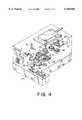
- FIG. 4is a perspective view of the polishing machine shown in FIG. 3;
- FIG. 5is a partially cutaway perspective view of the primary polishing station in the polishing machine in accordance with the invention.
- FIG. 6is a perspective view of a polishing head in the polishing machine in accordance with the invention, showing the internal structure of the head;
- FIG. 7is a perspective view of a vacuum chuck in the polishing machine in accordance with the invention.
- FIG. 8is an exploded perspective view of a polishing head in a polishing machine in accordance with the invention, showing the internal structure of the head;
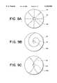
- FIG. 9Ais a plan view of a polishing cloth (pad) for use in the polishing machine in accordance with the invention, and in which the cloth is provided with slurry guide grooves;
- FIG. 9Bis a view similar to FIG. 9A, but in which the polishing cloth is provided with a spiral slurry guide groove;
- FIG. 9Cis a view similar to FIG. 9A, but in which the polishing cloth is provided with curved slurry guide grooves;
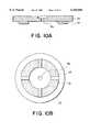
- FIG. 10Ais a cross-sectional view of another polishing cloth for use in the polishing machine in accordance with the invention, illustrating the manner in which the cloth is placed;
- FIG. 10Bis a bottom view of the polishing cloth shown in FIG. 10A;
- FIG. 11is a front elevation of a polishing head in the polishing machine in accordance with the invention, and in which the head starts to polish a wafer;
- FIG. 12is a front elevation of the polishing head shown in FIG. 11, and in which the head is polishing the wafer;
- FIG. 13is a front elevation similar to FIG. 12, but in which the polishing cloth is being conditioned.
- FIGS. 3 and 4there is shown an automatic polishing machine embodying the concept of the present invention.
- This machinehas an index table 1 for holding wafers.
- a loading station S 1a primary polishing station S 2 for performing a rough polishing removal, a second polishing station S 3 for providing the final polishing step, and an unloading station S 4 are established on the index table 1. These stations are circumferentially spaced from each other on the table.
- a plurality of wafer holders 2 for holding wafersare arranged around the center of the surface of the index table 1. These wafer holders are rotated into the stations S 1 -S 4 in turn. These stations S 1 -S 4 are assigned to stop positions, respectively, of the index table 1.
- the loading station S 1wafers are conveyed onto the index table 1.
- the unloading station S 4the wafers are transported out of the index table 1.
- the primary polishing station S 2provides a region where the surface of each wafer conveyed onto the index table 1 is flattened.
- the second polishing station S 3the surfaces of the flattened wafers undergo a final polishing step.
- the wafers W stored in a wafer cassette 10are picked and transported onto a pin clamp 11 one by one by a robot arm 7.
- the rear surface of the waferis cleaned by a wafer rear surface-cleaning means 8.
- Each cleaned wafer Wis transported onto the holder 2 at the loading station S 1 , using a wafer chuck 7a.
- the waferis attracted and held to a vacuum chuck 4.
- the index table 1rotates through 90°
- the wafer W on the holder 2is conveyed into the primary polishing station S 2 .
- the wafer Wcan be conveyed onto the holder 2 at the loading station S 1 by the robot arm 7.
- the holder 2is cleaned by a wafer chuck-cleaning number 8a, which may recede from a solid line circle to a dot-dash line circle.
- the wafer Wis flattened by a polishing head 18 and sent to the second polishing station S 3 , where the wafer is finally polished by a polishing head 35. Then, the wafer is shifted to the unloading station S 4 , where it is cleaned with a wafer surface-cleaning means 38.
- the wafer surface-cleaning means 38may recede form a solid line circle to a dot-dash line circle.
- each wafer Wis transported from the holder 2 onto a pin clamp 40 by a wafer chuck 39a.
- the rear surface of the waferis cleaned by a wafer rear surface-cleaning means 42.
- the wafer Wmay be moved onto the pin clamp 40 by a wafer chuck 39a, and the rear-surface of the wafer may be cleaned by the wafer rear surface-cleaning means 42.
- the wafermay be transported onto a conveyor 41 by the robot arm 39. Subsequently, the wafer is carried onto the conveyer 41 from the pin clamp 40 by the robot arm 39 and sent out for the next processing step.
- the index table 1rotates through a given angle and shifts the holder 2 free of the wafer W to the loading station S 1 , and makes preparations for entry of the next wafer.
- the primary polishing station S 1has the polishing head 18, the pad conditioning means 19, and the pad cleaning means 20, as shown in FIGS. 4 and 5.
- the polishing head 18consists of an assembly of a pressure application cylinder 21, a base plate 22, and a polishing plate 23 having a polishing surface to which polishing cloth 24 is attached.
- the polishing cloth 24is a hard circular polishing pad.
- the head 18depends from a spindle 17 that holds the pressure application cylinder 21.
- the polishing head 18advances from its retracted position into a position located above the vacuum chuck 4 at the primary polishing station S 2 .
- the headlowers onto the wafer W attracted to the vacuum chuck 4, pressing the polishing cloth 24 against the surface of the wafer W.
- the headroughly polishes the surface to flatten it.
- This rough polishingis done by rotating the holder 2 holding the wafer W to rotate the polishing head 18 in one direction and supplying the slurry from slurry supply holes 18a formed at the center position of rotation and the peripheral position onto the polishing cloth 24, the slurry being sent by a slurry supply pump.
- the slurryis dispersed uniformly between the polishing cloth 24 and the wafer W.
- the holder 2can be rotated at a high speed.
- the pressureis 0.01 to 0.1 kg/cm 2 .
- the surface of the polishing cloth 24is provided with at least one diffusive groove 32 in communication with the slurry supply hole 18a.
- the slurry sent from the slurry supply hole 18ais guided toward the outer periphery of the polishing cloth 24 by the diffusive grooves 32, whereby the slurry is dispersed uniformly over the polishing surface.
- the diffusive grooves 32extend radially from the slurry supply hole 18a.
- one diffusive groove 32extends spirally from the slurry supply hole 18a.
- the diffusive grooves 32are curved lines extending from the center to the outer periphery. In this way, the diffusive grooves can be any arbitrary straight lines or curved lines running from the center to the outer periphery.
- the optimum material of the polishing clothis a film of hard high polymer such as foamed polyurethane, such as IC-1000 manufactured by Rodale Nitta Co., Ltd., Japan.
- the shape of the polishing cloth 24is not limited to circular form.
- the polishing cloth 24may assume an annular shape formed by cutting out an outer portion of a disk.
- the cloth 24is attached to the polishing plate 23.
- This polishing cloth 24is also provided with diffusive grooves 32 for dispersing polish slurry.
- the diffusive grooves 32may not extend to the outer periphery. That is, the grooves 32 may be formed within the polishing cloth. In this case, the ends of the diffusive grooves 32 are inside the polishing cloth and so movement of the slurry out of the polishing pad is suppressed. That is, the slurry can stay in the cloth for a longer time.
- the outside diameter of the polishing clothis from a value comparable to the diameter of the wafer to a value about half of the diameter of the wafer.
- the thickness of the grooves 32is approximately 0.5 to 5 mm.
- the outside diameter of the polishing cloth 24is 150 mm.
- the thickness of the clothis 3 mm.
- the width of the diffusive grooves 32is 2 mm. In this example, four diffusive grooves 32 are regularly circumferentially spaced from each other. No limitations are placed on the number of the grooves or on the arrangement.
- the polishing clothmay be fabricated by placing polishing cloth of foamed polyurethane on polyester fiber polishing cloth (such as SUB 400 manufactured by Rodale Nitta Co., Ltd.). Where the polishing cloth is circular or annular, the slurry contacts the surface of the polishing plate 23. Therefore, the polishing plate 23 must have sufficient resistance to chemicals.
- the polishing plate 23is a sintered alumina plate or a stainless steel plate to which a sintered alumina plate is bonded.
- This chuck 4has a water seal chamber 27 that is annular in shape and provided with an opening on its topside.
- the seal chamber 27is formed outside the opening regions of the attracting holes 26.
- the seal chamber 27is in communication with a water channel 28 connected to a side surface of the vacuum chuck 4.
- the water channel 28is connected with a water supply hole 30 extending to the inner surface of a fixed seal ring 29 that is on the side of the index table. Wash water is forced into the water supply hole 30 and made to overflow from the water seal chamber 27. This prevents the slurry from passing under the wafer W; otherwise, the wafer W would adhere to the wafer-holding surface during polish. Furthermore, the slurry is prevented from entering the attracting holes 26 in the vacuum chuck 4.
- the polishing head 18is an assembly of the pressure application cylinder 21, the base plate 22, and the polishing plate 23.
- a drive plate 3 and a diaphragm 5are mounted between the pressure application cylinder 21 and the base plate 22.
- the fringes of the laminate of the drive plate 3 and the diaphragm 5are supported by a flange 6, which is clamped to the lower end of the cylinder 21 by bolts 12a.
- the flange 6is annular and has an inwardly extending overhang 6a.
- the base plate 22is held on the overhang 6a.
- the polishing plate 23is mounted to the base plate 22 by bolts 12b.
- the diaphragm 5maintains the hermeticity between the pressure application cylinder 21 and the base plate 22.
- the drive plate 3can follow the movement of the base plate 22 in three dimensions and gives support strength to the base plate 22.
- the optimum materials of the diaphragm 5are synthetic rubber, natural rubber, fluororubber, and Bakelite resin. Note that no limitations are imposed on the material of the diaphragm as long as it can maintain the hermeticity between the pressure application cylinder 21 and the base plate 22 and move quite small distances in three dimensions.
- the drive plate 3is a metal plate provided with three sets of arc-shaped holes 9a, 9b, 9c, etc. to impart flexibility to the plate.
- the drive plate 3 and the diaphragm 5are inserted between the pressure application cylinder 21 and the base plate 22 to permit the base plate 22 to swing relative to the pressure application cylinder 21 in three dimensions.
- the drive plate 3is capable of transmitting rotation of the spindle 17 to the base plate 22 and of moving quite small distances in three dimensions, especially in the vertical direction.
- the arc-shaped holes 9are formed in the metal plate having a thickness of about 0.5 to 3 mm.
- the three sets of arc-shaped holes 9a, 9b, and 9care formed along coaxial arcs having different radii.
- the holeshave widths of about 3 to 30 mm.
- the outermost holes 9a and the innermost holes 9care on the same radial lines within the drive plate 3.
- the intermediate holes 9bare on different radial lines. In this way, the drive plate 3 can move quite small distances in three dimensions, especially in the vertical direction, while maintaining the rigidity.
- the swinging movement of the polishing head 18allows fine movements in three dimensions. This is quite important for the polishing machine in accordance with the present invention.
- the polishing head 18is supported by the carrier 13, as shown in FIG. 5.
- the carrier 13depends from a frame 50, as shown in FIG. 1.
- the carrier 13reciprocates between the holder 2 at the primary polishing station S 2 of the index table 1 and its retracted position remote from the table 1 while guided by a rail 14 mounted above the index table 1. If the polishing head 18 is made of a completely rigid body, it is necessary that the wafer surface and the rail 14 be completely parallel to each other.
- the polishing head 18when the polishing head 18 is fed along the rail 14, the polishing pressure varies, making nonuniform the amount of the polishing across the wafer surface.
- three-dimensional structural playis given to the polishing head 18 to compensate for variations in the polishing pressure due to insufficient mechanical accuracy of the rail 14 or surface irregularities of the wafer.
- the fine movement of the polishing head 18can be controlled by adjusting the pressure inside the pressure application cylinder 21. Since the rail 14 depends from the frame 50, effective use is made of the space above the index table 1. This saves the space occupied.
- the frame 50is mounted to the housing of the polishing machine and located over the housing.
- an external air supply tube 15supplies high-pressure air into the spindle 17 through a nozzle 16.
- high-pressure airis supplied into a pressurizing chamber 31 within the pressure application cylinder 21. Fine movements in three dimensions can be adjusted by adjusting the pressure inside the cylinder 21.
- the aforementioned slurry supply hole 18ais in communication with the slurry supply tube 30 inserted in the spindle 17 as shown in FIG. 6.
- the polishing head 18is detachably mounted to the spindle 17 and placed in position on the carrier 13.
- This carrier 13comprises an air cylinder 46 forming a vertical drive mechanism and an electric motor 47 forming a rotary drive mechanism, as shown in FIGS. 1 and 5.
- the air cylinder 46moves the polishing head 18 up and down.
- the motor 47rotates the polishing head.
- Another motor 48is mounted on the side of the rail 14 to feed the carrier 13. As the motor 48 turns, a feed screw 49 is rotated.
- the carrier 13is moved from its retracted position along the rail 14 by the rotation of the feed screw 49. Then, the carrier 13 is sent over the holder 2 at the station S 2 shown in FIG. 11.
- the movement of the carrier 13is controlled by the vertical drive mechanism 46 and lowered above the holder 2, as shown in FIG. 12.
- the polishing head 18is driven straight along the rail 14 and, at the same time, is rotated by the rotary drive mechanism 47. Consequently, the polishing head 18 polishes the wafer W rotating on the holder 2.
- the feed mechanism 48consisting of the motor as described above reciprocates the polishing head 18 set on the carrier 13 along the rail.
- the feed speedis controlled according to the polishing position. For example, when the center of the wafer is being polished at a lower peripheral speed, the feed speed is made lower. When peripheries of the wafer are being polished, the feed speed is increased. In this manner, the whole wafer can be polished uniformly.
- the pressure applied to the vertical drive mechanism 46is 0.05 to 1 kg/cm 2 .
- the rotating speed of the head 18is approximately 30 to 1000 rpm.
- the rotating speed of the waferis about 10 to 300 rpm.
- the direction of rotation of the polishing head 18may be identical or opposite to the direction of rotation of the wafer. For instance, the polishing head 18 rotating in a counterclockwise direction at 500 rpm is reciprocated at 0.5 cm/second on the wafer rotating in a clockwise direction at 30 rpm.
- the scanning speed of the polishing head 18is not required to be kept constant. In practice, polishing conditions are established by entering a rotating speed of the wafer, scanning coordinates within the wafer, a scanning speed, a range of reciprocating movement, a rotating speed, and a polishing pressure of the polishing head into a control computer incorporated in the present polishing machine.
- the carrier 13 including the rail 14, the vertical drive mechanism 46, and the rotary drive mechanism 47, the feed screw 49, etc.are covered by a cover 51 mounted to the frame 50.
- the pressure inside the cover 51is made negative by performing local evacuation. Dust and powder might be created by wear of the rail 14 and the feed screw 49. Oily components might be splashed from the vertical drive mechanism 46 and from the rotary drive mechanism 47.
- the cover 51prevents such dust, powder, and oily components from dropping on the index table 1.
- the torqueis transmitted to the base plate 22 via the laminate of the drive plate 3 and the diaphragm 5 within the pressure application cylinder 21.
- the slurry fed from the pumpis forced into the supply tube 30 from the slurry supply tube 25.
- the slurryis supplied onto the wafer from the supply hole 18a.
- the valveis switched to supply pure water into the slurry supply tube 25, replacing the slurry inside the supply tube 30 with pure water.
- the slurry on the waferis replaced by pure water during decreasing polishing pressure. This stops the progress of the polish.
- the supply tube 30is a metal tube whose inner wall is coated with polyfluoroethylene.
- the polishing head 18is covered by a hood 33 mounted to the carrier 13.
- wash (rinse) water fis continued to flow along the inner surface of the hood 33. This prevents splashing slurry from solidifying; otherwise, solidified abrasive would fall, thus damaging the wafer W.
- pure wateris also supplied from a sealing portion mounted at the periphery of the holder 2. As a result, the slurry is prevented from going to the rear surface of the substrate all the way.
- the polishing cloth 24 of the polishing head 18becomes clogged (i.e., the mesh becomes nonuniform). This is corrected by returning the polishing head 18 into its retracted position and conditioning the cloth by the pad conditioning means 19.
- This pad conditioning means 19has a pad conditioning disk 34 that rotates. As shown in FIG. 13, this disk 34 is pressed against the polishing cloth 24 of the polishing head 18 while rotating the disk, thus conditioning the cloth. At this time, pure water is supplied into the slurry supply tube 25. The surface of the polishing cloth 24 is washed with pure water discharged from the supply hole 18a.
- the pad conditioning disk 34is made of a plate on which diamond particles of 10 to 500 ⁇ m are electrodeposited. During conditioning of the polishing cloth, the diamond particles might come off. In the present polishing machine, the cloth 24 faces downward. Therefore, released diamond particles do not easily adhere to the polishing cloth.
- the polishing cloth 24When the polishing cloth 24 is conditioned, further high-pressure air is admitted into the pressurization chamber 31 of the pressure application cylinder 21 in FIG. 6 to press protruding fringes 22a of the base plate 22 against the protruding fringes 6a of the flange 6 via the diaphragm 5 with a given pressure higher than the polishing pressure.
- the base plate 22 to which the polishing cloth 24 is attachedis clamped against the pressure application cylinder 21, fastening the cloth 24.
- the pad cleaning means 20consisting of a brush is reciprocated while rotated. This removes abrasive particles and powder adhering to the surface of the polishing cloth 24. In this way, preparations are made for rough polishing of the next wafer.
- the index table 1is rotated through a given angle of 90° to transport the wafer W flattened by the rough polishing into the second polishing station S 3 .
- final polishingis performed to reduce the roughness of the surface of the wafer that has been flattened by the primary (rough) polishing.
- a polishing slurry for the final polishingmay be different from the slurry used in the primary polishing at the first polishing station S 2 .
- an acidic alumina slurry with pH of about 1 to 2is used as the polishing slurry to etch the copper at a high etch rate during the primary polishing.
- a weakly acidic silica slurry with pH of about 4 to 6.5is used to suppress etching of the copper. This prevents the copper buried in the openings from dishing.
- the second polishing station S 3is also fitted with the pad conditioning means 36 and the pad cleaning means 37 as well as the polishing head 35 in the same way as the primary polishing station S 2 .
- the wafer W transported into the second polishing station S 3is finally polished by the polishing head 35.
- the pad conditioning means 36 and the pad cleaning means 37condition and clean the polishing cloth of the polishing head 35, in exactly the same way as the processing performed at the primary polishing station S 2 .
- the wash wateris kept supplied during, before, and after the rough and final polishing operations. Except during the polishing of the wafer, the used rinse water is once stored in a water vessel 43, as shown in FIGS. 11 and 13.
- a discharge valve 44is opened to discharge the water to the outside.
- a recycle valve 45is opened to recover the water into the recycling piping together with the slurry supplied to the polishing head, as shown in FIG. 12.
- the discharged slurry recovered into the recycling pipingis diluted with pure water. Therefore, the discharged slurry is condensed with an ultrafilter and then it is reused as a slurry. At this time, Cu 2+ ions and so on in the discharged slurry are removed if necessary.
- the polishing pad used on the polishing head 35 mounted at the second polishing station S 3consists of a polishing cloth that is harder than the polishing cloth used on the polishing head 18 at the primary polishing station S 2 .
- the final polishing stepis performed for a longer time than the rough polishing step.
- polyurethane-impregnated polyester fiber polishing clothsuch as SUBA800 manufactured by Rodale Nitta Co., Ltd.
- the same hard polishing cloth as used at the primary polishing stationcan also be used.
- the index table 1rotates through a given angle. This transports the wafer W into the unloading station S 4 at the same time as surface of the index table 1 is cleaned by cleaning liquid.
- the scrubberhas a first processing chamber in which both front and rear surfaces of the wafer are simultaneously washed with brushes to remove slurry particles.
- an electrolyteis used as cleaning liquid.
- the surface of the waferis cleaned with pin brushes having a diameter of 10 to 20 mm.
- a weakly acidic liquid or electrolyte containing citric acid or a mixture of about 0.01 to 0.1% buffered HF and 1 to 20% hydrogen peroxide wateris used to clean the copper-buried wafer surface.
- pure wateris supplied onto the surface of the wafer while rotating the wafer at a high speed.
- a mixture of about 0.1-5% buffered HF and 1-20% hydrogen peroxide wateris supplied to the rear surface of the wafer.
- the waferis spin-cleaned.
- Pure wateris supplied onto both surfaces of the wafer and cleaned.
- the waferis spin-dried.
- This series of processing steps inside the scrubbercompletely removes the slurry particles.
- metals such as copperare removed from the surface of the interlayer dielectric film on the surface of the wafer and from the rear surface of the wafer. Then, the wafer is transported into the LSI production line.
- the index tableis rotated in given angular increments of 90°.
- the waferis sent through the primary polishing station S 2 and the second polishing station S 3 to perform the rough polishing and the final polishing.
- the waferis transported to the outside from the unloading station S 4 .
- the wafers introduced in successionare polished roughly and finally on the same index table 1. Note that the present invention is not limited to this embodiment. The invention can be applied to wafers and other substrates held on the index table 1 for flattening.
- the polishing surface of a substrate on the index table 1is always held upwardly.
- a polishing cloth pressed against the substrate surfacecan be swung finely in three dimensions.
- the swinging movementcan be controlled.
- the polishingis performed while supplying the slurry onto the polishing cloth directly.
- the polished surface of the substratecan be observed from above and its flatness can be viewed or measured.
- the flatnesscan be modified without interrupting the polishing operation.
- the polishing headcan be used to polish with a disk having a smaller diameter than the outside diameter of the substrate while rotating the disk at a high speed.
- the polishing cloth attached to the polishing headdeforms viscoelastically during polish, and deformation occurs in proportion to the elapsed time within a short time (0.1 second). Accordingly, if the relative speed between the substrate and the polishing cloth is increased, the cloth becomes apparently harder and thus can enhance the accuracy at which the substrate surface is polished.
- the polishing accuracyhas heretofore depended on only the viscoelastic characteristics of the polishing cloth. Therefore, parameters that can be adjusted are limited.
- the polishing clothWith respect to local polishing uniformity, the polishing cloth becomes apparently harder because the relative speed between the cloth and the substrate is high. Hence, flattening providing quite high uniformity can be accomplished.
- the flatness, the thickness, and the temperature of the polished surfacecan be monitored and measured. Therefore, flatness corrective pattern can be calculated from the information about the polished surface.
- the polishing conditionscan be established according to the circumstances of the polish.
- the cost of the used slurry and polishing clothaccounts for a major portion of the running cost of the polish.
- slurryis supplied onto a platen to which polishing cloth is attached, most of the slurry is discharged without being used for the polishing of the substrate.
- the slurryis compressed between the polishing cloth and the substrate through a spindle. Consequently, the slurry is used at a high efficiency for the polishing of the wafer. Since the total surface of the polishing cloth touches the substrate, the whole surface of the polishing cloth is used uniformly. Hence, the cloth is not wasted.
- the polishing clothcan be rejuvenated by pressing a pad conditioning disk against the cloth. At this time, high-pressure air is admitted into the pressure application cylinder. The base plate is made stationary. The polishing cloth is prevented from vibrating during polish.
Landscapes
- Engineering & Computer Science (AREA)
- Mechanical Engineering (AREA)
- Finish Polishing, Edge Sharpening, And Grinding By Specific Grinding Devices (AREA)
- Mechanical Treatment Of Semiconductor (AREA)
- Grinding-Machine Dressing And Accessory Apparatuses (AREA)
Abstract
Description
Claims (17)
Applications Claiming Priority (2)
| Application Number | Priority Date | Filing Date | Title |
|---|---|---|---|
| JP9-332019 | 1997-12-02 | ||
| JP33201997AJP3076291B2 (en) | 1997-12-02 | 1997-12-02 | Polishing equipment |
Publications (1)
| Publication Number | Publication Date |
|---|---|
| US6165056Atrue US6165056A (en) | 2000-12-26 |
Family
ID=18250240
Family Applications (1)
| Application Number | Title | Priority Date | Filing Date |
|---|---|---|---|
| US09/203,392Expired - LifetimeUS6165056A (en) | 1997-12-02 | 1998-12-02 | Polishing machine for flattening substrate surface |
Country Status (4)
| Country | Link |
|---|---|
| US (1) | US6165056A (en) |
| JP (1) | JP3076291B2 (en) |
| KR (1) | KR100315722B1 (en) |
| GB (1) | GB2331948B (en) |
Cited By (46)
| Publication number | Priority date | Publication date | Assignee | Title |
|---|---|---|---|---|
| US6379230B1 (en) | 1997-04-28 | 2002-04-30 | Nec Corporation | Automatic polishing apparatus capable of polishing a substrate with a high planarization |
| US6398906B1 (en)* | 1999-03-15 | 2002-06-04 | Mitsubishi Materials Corporation | Wafer transfer apparatus and wafer polishing apparatus, and method for manufacturing wafer |
| US6406357B1 (en)* | 1999-03-10 | 2002-06-18 | Hitachi, Ltd. | Grinding method, semiconductor device and method of manufacturing semiconductor device |
| US20020083577A1 (en)* | 2000-12-28 | 2002-07-04 | Hiroo Suzuki | Polishing member and apparatus |
| US20020173244A1 (en)* | 2001-03-28 | 2002-11-21 | Sinnosuke Sekiya | Polishing tool and polishing method and apparatus using same |
| US20030232581A1 (en)* | 2002-06-16 | 2003-12-18 | Soo-Jin Ki | Surface planarization equipment for use in the manufacturing of semiconductor devices |
| US20040134789A1 (en)* | 2000-05-26 | 2004-07-15 | Koji Mishima | Substrate processing apparatus and substrate plating apparatus |
| US20050000943A1 (en)* | 2003-05-30 | 2005-01-06 | Nikon Corporation | Processing apparatus, method for fabrication of semiconductor device by using the processing apparatus, and semiconductor device fabricated by this method |
| US6857950B2 (en) | 2000-09-21 | 2005-02-22 | Nikon Corporation | Polishing apparatus, semiconductor device manufacturing method using the polishing apparatus, and semiconductor device manufactured by the manufacturing method |
| US20050107016A1 (en)* | 2002-03-20 | 2005-05-19 | Nikon Corporation | Polishing equipment, and method of manufacturing semiconductor device using the equipment |
| US7121919B2 (en) | 2001-08-30 | 2006-10-17 | Micron Technology, Inc. | Chemical mechanical polishing system and process |
| US20070093188A1 (en)* | 2005-10-21 | 2007-04-26 | Nemoto Timothy T | Dental crown polishing apparatus |
| US7238087B1 (en) | 2006-03-29 | 2007-07-03 | Okamoto Machine Tool Works, Ltd. | Planarizing device and a planarization method for semiconductor substrates |
| US20070284338A1 (en)* | 2006-06-08 | 2007-12-13 | Yukiteru Matsui | Chemical mechanical polishing method |
| US20090209176A1 (en)* | 2008-02-14 | 2009-08-20 | Ebara Corporation | Method and apparatus for polishing object |
| US20110223836A1 (en)* | 2010-03-12 | 2011-09-15 | Duescher Wayne O | Three-point fixed-spindle floating-platen abrasive system |
| US20110223835A1 (en)* | 2010-03-12 | 2011-09-15 | Duescher Wayne O | Three-point spindle-supported floating abrasive platen |
| US20110223838A1 (en)* | 2010-03-12 | 2011-09-15 | Duescher Wayne O | Fixed-spindle and floating-platen abrasive system using spherical mounts |
| US20110223837A1 (en)* | 2010-03-12 | 2011-09-15 | Duescher Wayne O | Fixed-spindle floating-platen workpiece loader apparatus |
| US20120088441A1 (en)* | 2010-10-12 | 2012-04-12 | Disco Corporation | Processing apparatus having four processing units |
| US8337280B2 (en) | 2010-09-14 | 2012-12-25 | Duescher Wayne O | High speed platen abrading wire-driven rotary workholder |
| US20130017762A1 (en)* | 2011-07-15 | 2013-01-17 | Infineon Technologies Ag | Method and Apparatus for Determining a Measure of a Thickness of a Polishing Pad of a Polishing Machine |
| US8430717B2 (en) | 2010-10-12 | 2013-04-30 | Wayne O. Duescher | Dynamic action abrasive lapping workholder |
| US20130217306A1 (en)* | 2012-02-16 | 2013-08-22 | Taiwan Semiconductor Manufacturing Co., Ltd. | CMP Groove Depth and Conditioning Disk Monitoring |
| US8641476B2 (en) | 2011-10-06 | 2014-02-04 | Wayne O. Duescher | Coplanar alignment apparatus for rotary spindles |
| US8647170B2 (en) | 2011-10-06 | 2014-02-11 | Wayne O. Duescher | Laser alignment apparatus for rotary spindles |
| US8647172B2 (en) | 2010-03-12 | 2014-02-11 | Wayne O. Duescher | Wafer pads for fixed-spindle floating-platen lapping |
| US8696405B2 (en) | 2010-03-12 | 2014-04-15 | Wayne O. Duescher | Pivot-balanced floating platen lapping machine |
| US8758088B2 (en) | 2011-10-06 | 2014-06-24 | Wayne O. Duescher | Floating abrading platen configuration |
| US8845394B2 (en) | 2012-10-29 | 2014-09-30 | Wayne O. Duescher | Bellows driven air floatation abrading workholder |
| US8998677B2 (en) | 2012-10-29 | 2015-04-07 | Wayne O. Duescher | Bellows driven floatation-type abrading workholder |
| US8998678B2 (en) | 2012-10-29 | 2015-04-07 | Wayne O. Duescher | Spider arm driven flexible chamber abrading workholder |
| US9011207B2 (en) | 2012-10-29 | 2015-04-21 | Wayne O. Duescher | Flexible diaphragm combination floating and rigid abrading workholder |
| US9039488B2 (en) | 2012-10-29 | 2015-05-26 | Wayne O. Duescher | Pin driven flexible chamber abrading workholder |
| US9199354B2 (en) | 2012-10-29 | 2015-12-01 | Wayne O. Duescher | Flexible diaphragm post-type floating and rigid abrading workholder |
| US9233452B2 (en) | 2012-10-29 | 2016-01-12 | Wayne O. Duescher | Vacuum-grooved membrane abrasive polishing wafer workholder |
| US9566687B2 (en) | 2014-10-13 | 2017-02-14 | Sunedison Semiconductor Limited (Uen201334164H) | Center flex single side polishing head having recess and cap |
| US9604339B2 (en) | 2012-10-29 | 2017-03-28 | Wayne O. Duescher | Vacuum-grooved membrane wafer polishing workholder |
| CN108994694A (en)* | 2018-09-21 | 2018-12-14 | 山东职业学院 | A kind of machine die surfacing processing device |
| CN112059899A (en)* | 2019-06-10 | 2020-12-11 | 罗门哈斯电子材料Cmp控股股份有限公司 | Thin Film Fluoropolymer Composite CMP Pads |
| US10926378B2 (en) | 2017-07-08 | 2021-02-23 | Wayne O. Duescher | Abrasive coated disk islands using magnetic font sheet |
| CN114643531A (en)* | 2020-12-18 | 2022-06-21 | 应用材料公司 | Pad carrier for horizontal pre-cleaning module |
| US11440161B2 (en)* | 2018-01-05 | 2022-09-13 | Ebara Corporation | Polishing head for face-up type polishing apparatus, polishing apparatus including the polishing head, and polishing method using the polishing apparatus |
| US11691241B1 (en)* | 2019-08-05 | 2023-07-04 | Keltech Engineering, Inc. | Abrasive lapping head with floating and rigid workpiece carrier |
| US12257666B2 (en)* | 2019-01-31 | 2025-03-25 | Ebara Corporation | Surface height measurement method using dummy disk |
| US12420376B2 (en) | 2021-12-23 | 2025-09-23 | Globalwafers Co., Ltd. | Polishing head assembly having recess and cap |
Families Citing this family (22)
| Publication number | Priority date | Publication date | Assignee | Title |
|---|---|---|---|---|
| KR100553834B1 (en)* | 1999-12-27 | 2006-02-24 | 삼성전자주식회사 | Chemical mechanical polishing pad with structure for easy discharge of abrasive residue |
| US6585572B1 (en) | 2000-08-22 | 2003-07-01 | Lam Research Corporation | Subaperture chemical mechanical polishing system |
| US6640155B2 (en) | 2000-08-22 | 2003-10-28 | Lam Research Corporation | Chemical mechanical polishing apparatus and methods with central control of polishing pressure applied by polishing head |
| US6652357B1 (en) | 2000-09-22 | 2003-11-25 | Lam Research Corporation | Methods for controlling retaining ring and wafer head tilt for chemical mechanical polishing |
| US7481695B2 (en) | 2000-08-22 | 2009-01-27 | Lam Research Corporation | Polishing apparatus and methods having high processing workload for controlling polishing pressure applied by polishing head |
| US6471566B1 (en) | 2000-09-18 | 2002-10-29 | Lam Research Corporation | Sacrificial retaining ring CMP system and methods for implementing the same |
| US6443815B1 (en) | 2000-09-22 | 2002-09-03 | Lam Research Corporation | Apparatus and methods for controlling pad conditioning head tilt for chemical mechanical polishing |
| JP4580118B2 (en)* | 2001-03-28 | 2010-11-10 | 株式会社ディスコ | Polishing method and grinding / polishing method |
| JP4594545B2 (en)* | 2001-03-28 | 2010-12-08 | 株式会社ディスコ | Polishing apparatus and grinding / polishing machine including the same |
| JP5293153B2 (en)* | 2002-03-14 | 2013-09-18 | 株式会社ニコン | Process amount prediction method |
| JP4465645B2 (en) | 2003-06-03 | 2010-05-19 | 株式会社ニコン | Polishing apparatus and semiconductor device manufacturing method using the same |
| KR100512179B1 (en)* | 2003-06-19 | 2005-09-02 | 삼성전자주식회사 | chemical and mechanical polishing apparatus for manufacturing a semiconductor |
| JPWO2005016595A1 (en)* | 2003-08-19 | 2006-10-12 | 株式会社ニコン | Polishing apparatus, semiconductor device manufacturing method using the same, and semiconductor device manufactured by the method |
| JP4732736B2 (en)* | 2004-11-08 | 2011-07-27 | 株式会社岡本工作機械製作所 | Device wafer vacuum chuck system and method for polishing back surface of device wafer using the same |
| JP5257729B2 (en)* | 2007-08-01 | 2013-08-07 | 株式会社ニコン | Polishing equipment |
| KR100910315B1 (en)* | 2007-10-08 | 2009-07-31 | 한국기초과학지원연구원 | Polishing apparatus for aspheric optical system for surface profile correction |
| JP5614723B2 (en)* | 2011-01-07 | 2014-10-29 | 旭硝子株式会社 | Polishing apparatus and polishing method for workpiece |
| WO2014128754A1 (en)* | 2013-02-19 | 2014-08-28 | 株式会社Leap | Cmp apparatus and cmp method |
| JP2013173226A (en)* | 2013-04-25 | 2013-09-05 | Nikon Corp | Polishing apparatus |
| JP6856335B2 (en)* | 2016-09-06 | 2021-04-07 | 株式会社ディスコ | Processing equipment |
| KR102435926B1 (en)* | 2020-06-08 | 2022-08-25 | 에스케이실트론 주식회사 | Apparatus and method for polishing wafer |
| JP2023114225A (en)* | 2022-02-04 | 2023-08-17 | 株式会社ディスコ | Polishing equipment |
Citations (18)
| Publication number | Priority date | Publication date | Assignee | Title |
|---|---|---|---|---|
| GB2175517A (en)* | 1985-05-23 | 1986-12-03 | Exnii Metallorezh Stankov | Vertical spindle jig grinder |
| GB2219536A (en)* | 1988-06-08 | 1989-12-13 | Tokiwa Seiki Ind Co | Ultra-precision grinding machine |
| US4890420A (en)* | 1988-03-21 | 1990-01-02 | Hossein Azimi | Grinding machine |
| US4916868A (en)* | 1987-09-14 | 1990-04-17 | Peter Wolters Ag | Honing, lapping or polishing machine |
| GB2250947A (en)* | 1990-12-17 | 1992-06-24 | Maria Dolores Marin Martos | Stone cutting and polishing machine |
| GB2259662A (en)* | 1991-09-20 | 1993-03-24 | Essilor Int | Method and multi-axis numerically-controlled machine for machining lenses |
| JPH05138529A (en)* | 1991-11-15 | 1993-06-01 | Yokogawa Electric Corp | Polishing equipment |
| US5216843A (en)* | 1992-09-24 | 1993-06-08 | Intel Corporation | Polishing pad conditioning apparatus for wafer planarization process |
| JPH05309559A (en)* | 1992-05-12 | 1993-11-22 | Speedfam Co Ltd | Plane surface polishing method and device |
| JPH0752033A (en)* | 1993-08-06 | 1995-02-28 | Sumitomo Metal Ind Ltd | Polishing equipment |
| JPH08330261A (en)* | 1995-05-30 | 1996-12-13 | Tokyo Electron Ltd | Polishing method and its device |
| JPH0970751A (en)* | 1995-09-06 | 1997-03-18 | Ebara Corp | Polishing equipment |
| JPH09262743A (en)* | 1996-03-27 | 1997-10-07 | Nec Corp | Device and method for detecting final point to be polished |
| JPH09277160A (en)* | 1996-02-15 | 1997-10-28 | Tadahiro Omi | Chemical machinery polishing device and method thereof |
| JPH10160420A (en)* | 1996-12-03 | 1998-06-19 | Tokyo Seimitsu Co Ltd | Instrument for measuring thickness and thickness variation of wafer |
| US5895270A (en)* | 1995-06-26 | 1999-04-20 | Texas Instruments Incorporated | Chemical mechanical polishing method and apparatus |
| US5921855A (en)* | 1997-05-15 | 1999-07-13 | Applied Materials, Inc. | Polishing pad having a grooved pattern for use in a chemical mechanical polishing system |
| US5927264A (en)* | 1998-01-08 | 1999-07-27 | Worley; Kenneth | Extended wear stone polishing disk |
- 1997
- 1997-12-02JPJP33201997Apatent/JP3076291B2/ennot_activeExpired - Lifetime
- 1998
- 1998-12-01KRKR1019980052323Apatent/KR100315722B1/ennot_activeExpired - Lifetime
- 1998-12-02GBGB9826497Apatent/GB2331948B/ennot_activeExpired - Lifetime
- 1998-12-02USUS09/203,392patent/US6165056A/ennot_activeExpired - Lifetime
Patent Citations (19)
| Publication number | Priority date | Publication date | Assignee | Title |
|---|---|---|---|---|
| GB2175517A (en)* | 1985-05-23 | 1986-12-03 | Exnii Metallorezh Stankov | Vertical spindle jig grinder |
| US4916868A (en)* | 1987-09-14 | 1990-04-17 | Peter Wolters Ag | Honing, lapping or polishing machine |
| US4890420A (en)* | 1988-03-21 | 1990-01-02 | Hossein Azimi | Grinding machine |
| GB2219536A (en)* | 1988-06-08 | 1989-12-13 | Tokiwa Seiki Ind Co | Ultra-precision grinding machine |
| GB2250947A (en)* | 1990-12-17 | 1992-06-24 | Maria Dolores Marin Martos | Stone cutting and polishing machine |
| GB2259662A (en)* | 1991-09-20 | 1993-03-24 | Essilor Int | Method and multi-axis numerically-controlled machine for machining lenses |
| JPH05138529A (en)* | 1991-11-15 | 1993-06-01 | Yokogawa Electric Corp | Polishing equipment |
| JPH05309559A (en)* | 1992-05-12 | 1993-11-22 | Speedfam Co Ltd | Plane surface polishing method and device |
| US5216843A (en)* | 1992-09-24 | 1993-06-08 | Intel Corporation | Polishing pad conditioning apparatus for wafer planarization process |
| JPH0752033A (en)* | 1993-08-06 | 1995-02-28 | Sumitomo Metal Ind Ltd | Polishing equipment |
| JPH08330261A (en)* | 1995-05-30 | 1996-12-13 | Tokyo Electron Ltd | Polishing method and its device |
| US5895270A (en)* | 1995-06-26 | 1999-04-20 | Texas Instruments Incorporated | Chemical mechanical polishing method and apparatus |
| JPH0970751A (en)* | 1995-09-06 | 1997-03-18 | Ebara Corp | Polishing equipment |
| JPH09277160A (en)* | 1996-02-15 | 1997-10-28 | Tadahiro Omi | Chemical machinery polishing device and method thereof |
| US5931722A (en)* | 1996-02-15 | 1999-08-03 | Tadahiro Ohmi | Chemical mechanical polishing apparatus |
| JPH09262743A (en)* | 1996-03-27 | 1997-10-07 | Nec Corp | Device and method for detecting final point to be polished |
| JPH10160420A (en)* | 1996-12-03 | 1998-06-19 | Tokyo Seimitsu Co Ltd | Instrument for measuring thickness and thickness variation of wafer |
| US5921855A (en)* | 1997-05-15 | 1999-07-13 | Applied Materials, Inc. | Polishing pad having a grooved pattern for use in a chemical mechanical polishing system |
| US5927264A (en)* | 1998-01-08 | 1999-07-27 | Worley; Kenneth | Extended wear stone polishing disk |
Cited By (62)
| Publication number | Priority date | Publication date | Assignee | Title |
|---|---|---|---|---|
| US6379230B1 (en) | 1997-04-28 | 2002-04-30 | Nec Corporation | Automatic polishing apparatus capable of polishing a substrate with a high planarization |
| US6406357B1 (en)* | 1999-03-10 | 2002-06-18 | Hitachi, Ltd. | Grinding method, semiconductor device and method of manufacturing semiconductor device |
| US6398906B1 (en)* | 1999-03-15 | 2002-06-04 | Mitsubishi Materials Corporation | Wafer transfer apparatus and wafer polishing apparatus, and method for manufacturing wafer |
| US7208074B2 (en)* | 2000-05-26 | 2007-04-24 | Ebara Corporation | Substrate processing apparatus and substrate plating apparatus |
| US20060027452A1 (en)* | 2000-05-26 | 2006-02-09 | Koji Mishima | Substrate processing apparatus and substrate plating apparatus |
| US20040134789A1 (en)* | 2000-05-26 | 2004-07-15 | Koji Mishima | Substrate processing apparatus and substrate plating apparatus |
| US6857950B2 (en) | 2000-09-21 | 2005-02-22 | Nikon Corporation | Polishing apparatus, semiconductor device manufacturing method using the polishing apparatus, and semiconductor device manufactured by the manufacturing method |
| US20020083577A1 (en)* | 2000-12-28 | 2002-07-04 | Hiroo Suzuki | Polishing member and apparatus |
| US7736215B2 (en) | 2001-03-28 | 2010-06-15 | Disco Corporation | Polishing tool and polishing method and apparatus using same |
| US20020173244A1 (en)* | 2001-03-28 | 2002-11-21 | Sinnosuke Sekiya | Polishing tool and polishing method and apparatus using same |
| US7713107B2 (en) | 2001-03-28 | 2010-05-11 | Disco Corporation | Polishing tool |
| US20070145011A1 (en)* | 2001-08-30 | 2007-06-28 | Micron Technology, Inc. | Chemical mechanical polishing system and process |
| US7121919B2 (en) | 2001-08-30 | 2006-10-17 | Micron Technology, Inc. | Chemical mechanical polishing system and process |
| US20060252350A1 (en)* | 2001-08-30 | 2006-11-09 | Micron Technology Inc. | Chemical mechanical polishing system and process |
| US20050107016A1 (en)* | 2002-03-20 | 2005-05-19 | Nikon Corporation | Polishing equipment, and method of manufacturing semiconductor device using the equipment |
| US20030232581A1 (en)* | 2002-06-16 | 2003-12-18 | Soo-Jin Ki | Surface planarization equipment for use in the manufacturing of semiconductor devices |
| US6846224B2 (en)* | 2002-07-16 | 2005-01-25 | Samsung Electronics Co., Ltd. | Surface planarization equipment for use in the manufacturing of semiconductor devices |
| US20050000943A1 (en)* | 2003-05-30 | 2005-01-06 | Nikon Corporation | Processing apparatus, method for fabrication of semiconductor device by using the processing apparatus, and semiconductor device fabricated by this method |
| US7422514B2 (en)* | 2005-10-21 | 2008-09-09 | Timothy Tamio Nemoto | Dental crown polishing apparatus |
| US20070093188A1 (en)* | 2005-10-21 | 2007-04-26 | Nemoto Timothy T | Dental crown polishing apparatus |
| US7238087B1 (en) | 2006-03-29 | 2007-07-03 | Okamoto Machine Tool Works, Ltd. | Planarizing device and a planarization method for semiconductor substrates |
| US20070284338A1 (en)* | 2006-06-08 | 2007-12-13 | Yukiteru Matsui | Chemical mechanical polishing method |
| US20090209176A1 (en)* | 2008-02-14 | 2009-08-20 | Ebara Corporation | Method and apparatus for polishing object |
| US8257143B2 (en) | 2008-02-14 | 2012-09-04 | Ebara Corporation | Method and apparatus for polishing object |
| US20110223838A1 (en)* | 2010-03-12 | 2011-09-15 | Duescher Wayne O | Fixed-spindle and floating-platen abrasive system using spherical mounts |
| US20110223835A1 (en)* | 2010-03-12 | 2011-09-15 | Duescher Wayne O | Three-point spindle-supported floating abrasive platen |
| US20110223837A1 (en)* | 2010-03-12 | 2011-09-15 | Duescher Wayne O | Fixed-spindle floating-platen workpiece loader apparatus |
| US8740668B2 (en) | 2010-03-12 | 2014-06-03 | Wayne O. Duescher | Three-point spindle-supported floating abrasive platen |
| US20110223836A1 (en)* | 2010-03-12 | 2011-09-15 | Duescher Wayne O | Three-point fixed-spindle floating-platen abrasive system |
| US8328600B2 (en) | 2010-03-12 | 2012-12-11 | Duescher Wayne O | Workpiece spindles supported floating abrasive platen |
| US8602842B2 (en) | 2010-03-12 | 2013-12-10 | Wayne O. Duescher | Three-point fixed-spindle floating-platen abrasive system |
| US8696405B2 (en) | 2010-03-12 | 2014-04-15 | Wayne O. Duescher | Pivot-balanced floating platen lapping machine |
| US8647171B2 (en) | 2010-03-12 | 2014-02-11 | Wayne O. Duescher | Fixed-spindle floating-platen workpiece loader apparatus |
| US8500515B2 (en) | 2010-03-12 | 2013-08-06 | Wayne O. Duescher | Fixed-spindle and floating-platen abrasive system using spherical mounts |
| US8647172B2 (en) | 2010-03-12 | 2014-02-11 | Wayne O. Duescher | Wafer pads for fixed-spindle floating-platen lapping |
| US8337280B2 (en) | 2010-09-14 | 2012-12-25 | Duescher Wayne O | High speed platen abrading wire-driven rotary workholder |
| US8430717B2 (en) | 2010-10-12 | 2013-04-30 | Wayne O. Duescher | Dynamic action abrasive lapping workholder |
| US8657648B2 (en)* | 2010-10-12 | 2014-02-25 | Disco Corporation | Processing apparatus having four processing units |
| US20120088441A1 (en)* | 2010-10-12 | 2012-04-12 | Disco Corporation | Processing apparatus having four processing units |
| US20130017762A1 (en)* | 2011-07-15 | 2013-01-17 | Infineon Technologies Ag | Method and Apparatus for Determining a Measure of a Thickness of a Polishing Pad of a Polishing Machine |
| US8641476B2 (en) | 2011-10-06 | 2014-02-04 | Wayne O. Duescher | Coplanar alignment apparatus for rotary spindles |
| US8647170B2 (en) | 2011-10-06 | 2014-02-11 | Wayne O. Duescher | Laser alignment apparatus for rotary spindles |
| US8758088B2 (en) | 2011-10-06 | 2014-06-24 | Wayne O. Duescher | Floating abrading platen configuration |
| US20130217306A1 (en)* | 2012-02-16 | 2013-08-22 | Taiwan Semiconductor Manufacturing Co., Ltd. | CMP Groove Depth and Conditioning Disk Monitoring |
| US9039488B2 (en) | 2012-10-29 | 2015-05-26 | Wayne O. Duescher | Pin driven flexible chamber abrading workholder |
| US8998678B2 (en) | 2012-10-29 | 2015-04-07 | Wayne O. Duescher | Spider arm driven flexible chamber abrading workholder |
| US9011207B2 (en) | 2012-10-29 | 2015-04-21 | Wayne O. Duescher | Flexible diaphragm combination floating and rigid abrading workholder |
| US8845394B2 (en) | 2012-10-29 | 2014-09-30 | Wayne O. Duescher | Bellows driven air floatation abrading workholder |
| US9199354B2 (en) | 2012-10-29 | 2015-12-01 | Wayne O. Duescher | Flexible diaphragm post-type floating and rigid abrading workholder |
| US9233452B2 (en) | 2012-10-29 | 2016-01-12 | Wayne O. Duescher | Vacuum-grooved membrane abrasive polishing wafer workholder |
| US9604339B2 (en) | 2012-10-29 | 2017-03-28 | Wayne O. Duescher | Vacuum-grooved membrane wafer polishing workholder |
| US8998677B2 (en) | 2012-10-29 | 2015-04-07 | Wayne O. Duescher | Bellows driven floatation-type abrading workholder |
| US9566687B2 (en) | 2014-10-13 | 2017-02-14 | Sunedison Semiconductor Limited (Uen201334164H) | Center flex single side polishing head having recess and cap |
| US10926378B2 (en) | 2017-07-08 | 2021-02-23 | Wayne O. Duescher | Abrasive coated disk islands using magnetic font sheet |
| US11440161B2 (en)* | 2018-01-05 | 2022-09-13 | Ebara Corporation | Polishing head for face-up type polishing apparatus, polishing apparatus including the polishing head, and polishing method using the polishing apparatus |
| CN108994694A (en)* | 2018-09-21 | 2018-12-14 | 山东职业学院 | A kind of machine die surfacing processing device |
| CN108994694B (en)* | 2018-09-21 | 2020-04-21 | 山东职业学院 | Mechanical die surfacing processing device |
| US12257666B2 (en)* | 2019-01-31 | 2025-03-25 | Ebara Corporation | Surface height measurement method using dummy disk |
| CN112059899A (en)* | 2019-06-10 | 2020-12-11 | 罗门哈斯电子材料Cmp控股股份有限公司 | Thin Film Fluoropolymer Composite CMP Pads |
| US11691241B1 (en)* | 2019-08-05 | 2023-07-04 | Keltech Engineering, Inc. | Abrasive lapping head with floating and rigid workpiece carrier |
| CN114643531A (en)* | 2020-12-18 | 2022-06-21 | 应用材料公司 | Pad carrier for horizontal pre-cleaning module |
| US12420376B2 (en) | 2021-12-23 | 2025-09-23 | Globalwafers Co., Ltd. | Polishing head assembly having recess and cap |
Also Published As
| Publication number | Publication date |
|---|---|
| GB2331948B (en) | 2002-07-31 |
| JP3076291B2 (en) | 2000-08-14 |
| KR19990062699A (en) | 1999-07-26 |
| JPH11156711A (en) | 1999-06-15 |
| GB2331948A (en) | 1999-06-09 |
| GB9826497D0 (en) | 1999-01-27 |
| KR100315722B1 (en) | 2002-01-15 |
Similar Documents
| Publication | Publication Date | Title |
|---|---|---|
| US6165056A (en) | Polishing machine for flattening substrate surface | |
| US6241585B1 (en) | Apparatus and method for chemical mechanical polishing | |
| US7241203B1 (en) | Six headed carousel | |
| US6722964B2 (en) | Polishing apparatus and method | |
| US6869337B2 (en) | System and method for polishing and planarizing semiconductor wafers using reduced surface area polishing pads and variable partial pad-wafer overlapping techniques | |
| EP0874390B1 (en) | Polishing method | |
| EP1250215B1 (en) | System and method for controlled polishing and planarization of semiconductor wafers | |
| JP2007260850A (en) | Flattening device of semiconductor substrate and flattening method | |
| JP2010064196A (en) | Substrate polishing device and substrate polishing method | |
| JP2001129754A (en) | Method and apparatus for measuring pad profile, and closed loop control of pad conditioning process | |
| US10256120B2 (en) | Systems, methods and apparatus for post-chemical mechanical planarization substrate buff pre-cleaning | |
| US20050070215A1 (en) | Chemical mechanical polishing apparatus having conditioning cleaning device | |
| US6758726B2 (en) | Partial-membrane carrier head | |
| US6908371B2 (en) | Ultrasonic conditioning device cleaner for chemical mechanical polishing systems | |
| KR100506814B1 (en) | Apparatus for polishing a wafer | |
| US20020016136A1 (en) | Conditioner for polishing pads | |
| KR20070077979A (en) | Chemical mechanical polishing apparatus and wafer polishing method using the same | |
| WO2004059714A1 (en) | Polishing device and method of producing semiconductor device | |
| JPH10264011A (en) | Precision polishing apparatus and method | |
| US20240383092A1 (en) | Polishing tool and method | |
| JP2001351884A (en) | Chemical mechanical polishing apparatus for substrate | |
| KR200201955Y1 (en) | Cmp for lager diameter of silicon wafer and method using the cmp machine | |
| JP2000254856A (en) | Polishing apparatus and polishing method | |
| EP1297927A2 (en) | Polishing apparatus |
Legal Events
| Date | Code | Title | Description |
|---|---|---|---|
| AS | Assignment | Owner name:OKAMOTO MACHINE TOOL WORKS, LTD., JAPAN Free format text:ASSIGNMENT OF ASSIGNORS INTEREST;ASSIGNORS:HAYASHI, YOSHIHIRO;ONODERA, TAKAHIRO;KOBAYASHI, KAZUO;REEL/FRAME:009626/0436 Effective date:19981127 Owner name:NEC CORPORATION, JAPAN Free format text:ASSIGNMENT OF ASSIGNORS INTEREST;ASSIGNORS:HAYASHI, YOSHIHIRO;ONODERA, TAKAHIRO;KOBAYASHI, KAZUO;REEL/FRAME:009626/0436 Effective date:19981127 | |
| AS | Assignment | Owner name:NIKON CORPORATION, JAPAN Free format text:ASSIGNMENT OF ASSIGNORS INTEREST;ASSIGNOR:OKAMOTO MACHINE TOOL WORKS, LTD.;REEL/FRAME:011048/0725 Effective date:20000331 | |
| FEPP | Fee payment procedure | Free format text:PAYOR NUMBER ASSIGNED (ORIGINAL EVENT CODE: ASPN); ENTITY STATUS OF PATENT OWNER: LARGE ENTITY | |
| STCF | Information on status: patent grant | Free format text:PATENTED CASE | |
| FPAY | Fee payment | Year of fee payment:4 | |
| FPAY | Fee payment | Year of fee payment:8 | |
| FPAY | Fee payment | Year of fee payment:12 |