US6164241A - Multiple coil antenna for inductively-coupled plasma generation systems - Google Patents
Multiple coil antenna for inductively-coupled plasma generation systemsDownload PDFInfo
- Publication number
- US6164241A US6164241AUS09/106,852US10685298AUS6164241AUS 6164241 AUS6164241 AUS 6164241AUS 10685298 AUS10685298 AUS 10685298AUS 6164241 AUS6164241 AUS 6164241A
- Authority
- US
- United States
- Prior art keywords
- antenna
- coil
- antenna segments
- plasma
- segments
- Prior art date
- Legal status (The legal status is an assumption and is not a legal conclusion. Google has not performed a legal analysis and makes no representation as to the accuracy of the status listed.)
- Expired - Lifetime
Links
- 239000003990capacitorSubstances0.000claimsabstractdescription86
- 230000008878couplingEffects0.000claimsabstractdescription34
- 238000010168coupling processMethods0.000claimsabstractdescription34
- 238000005859coupling reactionMethods0.000claimsabstractdescription34
- 238000000034methodMethods0.000claimsdescription19
- 230000008569processEffects0.000claimsdescription17
- 230000008859changeEffects0.000claimsdescription10
- 238000009826distributionMethods0.000claimsdescription8
- 238000009616inductively coupled plasmaMethods0.000claimsdescription6
- 230000007423decreaseEffects0.000claimsdescription4
- 238000006243chemical reactionMethods0.000claims7
- 230000005672electromagnetic fieldEffects0.000claims6
- 230000001939inductive effectEffects0.000abstractdescription13
- 210000002381plasmaAnatomy0.000description69
- 230000005684electric fieldEffects0.000description7
- 230000000694effectsEffects0.000description6
- 238000009792diffusion processMethods0.000description5
- 230000009977dual effectEffects0.000description5
- 230000005540biological transmissionEffects0.000description4
- 230000003247decreasing effectEffects0.000description3
- 239000004065semiconductorSubstances0.000description3
- 230000008901benefitEffects0.000description2
- 239000002131composite materialSubstances0.000description2
- 230000007812deficiencyEffects0.000description2
- 238000005530etchingMethods0.000description2
- 150000002500ionsChemical class0.000description2
- 238000012545processingMethods0.000description2
- 238000000151depositionMethods0.000description1
- 230000008021depositionEffects0.000description1
- 239000003989dielectric materialSubstances0.000description1
- 239000003574free electronSubstances0.000description1
- 238000010849ion bombardmentMethods0.000description1
- 238000004519manufacturing processMethods0.000description1
- 239000000463materialSubstances0.000description1
- 238000005259measurementMethods0.000description1
- 230000009467reductionEffects0.000description1
- 238000011160researchMethods0.000description1
- 239000007787solidSubstances0.000description1
- 239000000758substrateSubstances0.000description1
- 238000012546transferMethods0.000description1
Images


Classifications
- H—ELECTRICITY
- H01—ELECTRIC ELEMENTS
- H01J—ELECTRIC DISCHARGE TUBES OR DISCHARGE LAMPS
- H01J37/00—Discharge tubes with provision for introducing objects or material to be exposed to the discharge, e.g. for the purpose of examination or processing thereof
- H01J37/32—Gas-filled discharge tubes
- H—ELECTRICITY
- H01—ELECTRIC ELEMENTS
- H01J—ELECTRIC DISCHARGE TUBES OR DISCHARGE LAMPS
- H01J37/00—Discharge tubes with provision for introducing objects or material to be exposed to the discharge, e.g. for the purpose of examination or processing thereof
- H01J37/32—Gas-filled discharge tubes
- H01J37/32009—Arrangements for generation of plasma specially adapted for examination or treatment of objects, e.g. plasma sources
- H01J37/32082—Radio frequency generated discharge
- H01J37/321—Radio frequency generated discharge the radio frequency energy being inductively coupled to the plasma
Definitions
- the present inventionrelates to plasma reactors for processing materials such as semiconductor substrates. More particularly, the present invention relates to a system for improving the inductive coupling uniformity within plasma reactors.
- Plasma generationis useful in a variety of semiconductor fabrication processes, for example plasma enhanced etching and deposition.
- Plasmasare generally produced from a low pressure gas by electric field ionization and generation of free electrons which ionize individual gas molecules through the transfer of kinetic energy via individual electron-gas molecule collisions.
- the electronsare commonly accelerated in an electric field, typically a radio frequency electric field.
- FIG. 1schematically illustrates a plasma generating device 100 which includes an antenna system 105, a dielectric window 120, a gas distribution plate 130, a wafer to be processed 140, a vacuum chamber 150, an electrostatic chuck 160, and a lower electrode 170.
- a radio frequency source(not shown) is used to provide a radio frequency current to the antenna system 105, typically via a radio frequency matching circuit (also not shown).
- the radio frequency currentresonates through the antenna system 105, inducing an azimuthal electric field within the vacuum chamber 150.
- a process gasis introduced into the vacuum chamber 150 via the gas distribution plate 130, and the induced electric field ionizes the process gas to produce a plasma within the chamber 150.
- the plasmathen impinges upon the wafer 140 (which (which is held in place by way of the electrostatic chuck 160) and processes (e.g., etching) the wafer 140 as desired.
- Another radio frequencyat a frequency which is different from that applied to the antenna coil, is typically applied to the lower electrode 170 to provide a negative DC bias voltage for ion bombardment.
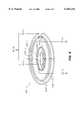
- FIGS. 2A and 2Bdepict two planar spiral coils 110a, 110b which make up the antenna system illustrated in the '458 patent.
- a first planar coil 110ais constructed as a singular conductive element formed into a planar spiral and connected to radio frequency taps 205, 215 for connection to radio frequency circuitry.
- an alternative planar coil 110bis constructed as a plurality of concentric rings 220 connected in series via inter-connectors 225 and coupled at each end to radio frequency taps 205, 215.
- the circular current pattern provided by such spiral coilscreates toroidal-shaped plasmas which can in turn cause radial non-uniformity in the etch rate at the wafer 140.
- the coil antenna 110produces a toroidal plasma having a lower density in the center, and must rely on plasma diffusion (i.e., the diffusion of electrons and ions into the center) in order to provide reasonable uniformity at the center of the toroid. In certain applications, however, the uniformity provided by plasma diffusion is insufficient.
- spiral coil antennastend to make azimuthal non-uniform plasma.
- the voltage and current wavestravel forward from the input end to the terminal end, and will be reflected back at the terminal end.
- the superposition of the forward and reflected wavesresults in a standing wave on the coil (i.e., the voltage and current vary periodically along the length of the coil). If the coil is grounded at the terminal end, the current at the terminal end is at a maximum value, and the voltage at the terminal end is zero.
- the planar coilis typically terminated with a capacitance such that the current in the coil is similar at both ends of the coil and increases to a maximum near the middle of the coil. Doing so can improve plasma uniformity, but azimuthal non-uniformity still exists because the current varies in the azimuthal direction along the length of the coil. For example, point P in FIG. 2A is the current maximum. On either side of point P the current drops off. Therefore, the power coupling to the plasma is higher beneath P and the corresponding plasma is denser. In contrast, the plasma density at point P' is relatively lower.
- the terminating capacitor valuecan be varied, doing so only changes the position of the voltage null along the coil.
- the coilcan be terminated with an inductance in order to provide the same polarity voltage along the coil length, a current null will exist somewhere in the central portion of the coil (with the current traveling in opposite directions on either side of the null), and the resulting plasma density can be unacceptably low and non-uniform.
- U.S. Pat. No. 5,401,350 to Patrick et al.attempts to overcome the above-described deficiencies. Therein, a multiple planar coil configuration is set forth in order to improve plasma uniformity. The RF power to the individual coils is independently controlled, requiring separate power supplies and separate matching networks which allow for independent adjustment of the power and phase.
- the present inventionovercomes the above-identified deficiencies in the art by providing a system for improving the inductive coupling uniformity within an antenna system. By controlling the positioning and current distribution of the antenna coils, plasma uniformity can be improved.
- two or more spiral coilsare positioned on a dielectric window of a plasma chamber.
- Each coilis either planar or a combination of both a planar coil and a vertically stacked helical coil.
- the input end of each coilis attached to an input variable capacitor and the output end is terminated to the ground through an output variable capacitor.
- the output capacitordetermines where the current is an extreme (i.e., a maximum or a minimum) or the voltage is an extreme, while the input capacitor can change the overall impedance of each coil, and therefore, the ratio of current magnitudes in these multiple coils can be adjusted.
- FIG. 1depicts a plasma reactor wherein an antenna system is placed at the top of the dielectric window and is used to couple radio frequency energy into a processing chamber;
- FIGS. 2A and 2Bdepict two conventional planar spiral coil antennas
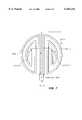
- FIG. 3depicts an exemplary arrangement of dual, single-turn planar coils according to a first embodiment of the present invention
- FIG. 4depicts an exemplary arrangement of dual, multiple-turn planar coils according to a second embodiment of the present invention
- FIG. 5depicts an exemplary arrangement of dual, multiple-turn planar coils with an inner helical coil according to a third embodiment of the present invention
- FIG. 6depicts an exemplary arrangement of dual, multiple-turn planar coils, with both inner and outer helical coils according to a fourth embodiment of the present invention.
- FIG. 7depicts an exemplary arrangement of dual, multiple-turn planar coils with parallel antenna elements according to a fifth embodiment of the present invention.
- FIG. 1depicts a plasma generating device 100 in which the antenna system of the present invention may be incorporated.
- the plasma generating device 100includes a dielectric window 120, a gas distribution plate 130, a wafer 140, a vacuum chamber 150, an electrostatic chuck 160, a lower electrode 170 and an antenna system 105.
- the antenna system 105includes a set of coils 110 which is connected to a RF matching network (not shown) and a RF generator (not shown).
- the antenna systemis a Transformer-Coupled Plasma (TCPTM, a registered trademark of Lam Research Corporation) antenna system.
- FIG. 3illustrates the TCPTM antenna system 300 according to a first embodiment of the present invention.
- the TCPTM system 300includes two single-turn coils. Coil 1 is preferably placed near the center while Coil 2 is preferably placed further toward the outer edge of the reactor's top opening.
- a radio frequency (RF) currentis simultaneously provided to one end of Coils 1 and 2 via two tuning capacitors C 1 and C 2 .
- the RF inputis generated by a RF source 310 and fed to capacitors C 1 and C 2 through a RF matching network 320.
- Tuning capacitors C 1 and C 2allow for the magnitude of currents I 1 , and I 2 in Coils 1 and 2, respectively, to be adjusted.
- the opposite ends of Coil 1 and Coil 2are tied together and terminated to ground through impedance Z T .
- a planar coil antennaproduces a toroidal plasma with a radius which is close to one half of the driving coil's radius. By placing two coils apart, this effectively generates a more gradual plasma toroid having a radius that is approximately equal to one half of the mean radii of the two coils.
- the power coupling to the plasma from the inner coilis localized in the inner region while the power coupling from the outer coil is localized in the outer region.
- plasma diffusioni.e., the diffusion of electrons and ions
- the circuitry associated with the two single-turn coilsi.e., the capacitors C 1 and C 2 and impedance Z T ) is capable of adjusting the ratio of current magnitudes in Coil 1 and Coil 2, i.e., I 1 and I 2 , respectively.
- I 1 and I 2the ratio of current magnitudes in Coil 1 and Coil 2, i.e., I 1 and I 2 , respectively.
- C 1 and C 2may be either fixed or variable capacitors.
- Input tuning capacitors C 1 and C 2partially cancel the input inductive reactance of each coil.
- the input reactance of each legis the same, resulting in equal input currents into Coil 1 and Coil 2 when fed from a common source. Adjusting C 1 higher and C 2 lower from these starting values causes decreased current in Coil 1 and increased current in Coil 2. Reversing the direction causes the current to be unbalanced in the opposite direction.
- the input impedance of the composite circuitremains nominally the same during the adjustment process since one leg has increased reactance while the other leg has decreased reactance.
- Z Tcan be a common capacitor, as in conventional TCPTM systems, or an electrically short connection to the ground. Z T could also be represented as separate capacitors terminated to the ground. If each coil has a different electrical length, the input impedance of each coil is also different. Separate terminating capacitors can be chosen so that the current maximum occurs nominally at the center of each coil length.
- the use of two single-turn coils as described aboveis provided merely for explanatory purposes.
- the general principles set forth aboveare equally applicable to multiple-coil, multiple-turn systems.
- the present inventionis not limited to two dimensional coil configurations (as illustrated in FIG. 3), but may alternatively be implemented as three dimensional coil configurations.
- the coilscan be arranged to conform to a dome-shaped dielectric window or arranged helically around a cylindrical dielectric window.
- the principles set forth aboveare equally applicable to domed, helical, or other three-dimensional configurations having multiple coils with multiple turns.
- FIG. 4illustrates the TCPTM antenna system 400 according to a second embodiment of the present invention.
- two multiple-turn coils(Coil 1 and Coil 2) are provided having four tuning capacitors C 1 -C 4 attached thereto.
- Coil 1is positioned in the center, while Coil 2 is preferably positioned further toward the outer edge of the reactor's top opening.
- the RF inputis simultaneously fed to a first end of Coils 1 and 2 through tuning capacitors C 1 and C 2 , respectively.
- the opposite ends of Coils 1 and 2are terminated through tuning capacitors C 3 and C 4 , respectively.
- the two coilseffectively generate a more gradual toroidal-shaped plasma.
- the power couplings to the plasma from the coilsspread out over the entire region and produce a single flattened toroidal-shaped plasma. If the currents are unbalanced, the toroidal field can be stronger in the center or at the outside.
- Two capacitorsare provided for each coil so as to obtain a more symmetric current distribution along the coil. For example, one can adjust C 1 together with C 3 so that the current maximum (as well as the purely resistive impedance point) occurs at the center of Coil 1. Moving from the center of the coil towards C 1 , the reactance is inductive, and moving from the center of the coil towards C 3 the reactance becomes capacitive, so that the current is maximum in the center and is reduced away from the center in a nominally sinusoidal fashion.
- adjustments of C 3 and C 4can compensate for the azimuthal non-uniform plasma described above. For example, one can adjust C 3 to achieve the maximum current at point P 1 of Coil 1 in FIG. 4. As a result, the power coupling to the plasma is higher beneath P 1 and the corresponding plasma density is higher. This tends to lead toward azimuthal non-uniformity. However, by adjusting C 4 , the maximum current can be achieved at location P 2 in Coil 2 along the same radial axis opposite P 1 . Therefore, a higher power coupling of Coil 2 at P 2 offsets the effect due to Coil 1, resulting in a more azimuthally uniform plasma. As an alternative to adjusting C 3 and C 4 , the azimuthal position of Coil 1 can be physically rotated relative to that of Coil 2, so that the current maxima in Coil 1 and Coil 2 occur at P 1 and P 2 , respectively.
- the tuning capacitors, C 1 and C 2can be arranged such that they turn in opposite directions with a single control.
- the current unbalance and hence, plasma uniformitycan be optimized with a single control from a single generator without disturbing the single conventional matching network at the input.
- adjusting C 3 and C 4 in opposite directionscan have the same effect as adjusting C 1 and C 2 .
- the mutual coupling between the coil and the plasmachanges in a manner similar to the mutual coupling between the primary coil (i.e., the driving coil) and secondary coil (i.e., the plasma) of a transformer (see Albert J. Lamm, "Observations of Standing Waves on an Inductive Plasma Coil Modeled as a Uniform Transmission Line," J. Vac. Sci. Tech. A, Vol. 15, No. 5, Sept./Oct. 1997, p. 2615).
- An increase/decrease in the number of turnsaffects the density of the plasma. For example, an increase in the number of turns can cause a reduction in the mutual coupling coefficient which thereby lowers the plasma density.
- the coil lengthis decreased, the overall plasma generation integrated over the coil length can be reduced. Therefore, one skilled in the art will appreciate that it is possible to optimize the number of turns and the overall length of each coil in order to balance these two factors.
- ⁇ , ⁇ and the effective characteristic impedance Zoare assumed to be the same throughout the three situations.
- Table Iprovides the values for ⁇ , ⁇ , Zo, the electrical length of each coil, and C 1 -C 4 .
- Z inrepresents the input impedance of each coil.
- the overall input impedance of the two coilsis 2.1+j10.5 ⁇ which is approximately half of Z in for each coil.
- Table IIlists the magnitudes and phase angles of I i , I i ', V i , and V i ' for the i-th coil when an input RF power of 1000 W and the parameters described in Table I are provided.
- I i 'represents the current at the output end (closer to C 3 and C 4 in FIG. 4) of the i-th coil
- V i and V i 'represent the voltage at the input and the output ends of the i-th coil, respectively.
- the RF current and voltageare unbalanced between the two coils, but are balanced within each coil.
- Both the current and voltage in the inner coil (Coil 1)are 34% less than those in the outer coil (Coil 2) since the overall impedance of the inner coil is higher than that of the outer coil.
- Each coilis symmetrically balanced around the coil center, so that the values of the input current and voltage in each coil are almost equal to the output values in magnitude. Away from each coil's center the impedance is inductively-dominated toward the input end of the coil and capacitively-dominated toward the output end; this is evident from the phase angle change between the input and output voltage.
- the overall input impedance of the two coilsis 2.0+j11.4 ⁇ which is approximately half of Z in for each coil.
- Table IVlists the magnitudes and phase angles of I i , I i ', V i , and V i ' for the i-th coil when an input RF power of 1000 W and the parameters described in Table III are provided.
- the final situationillustrates the effect of varying the values of C 1 and C 2 such that the value of C 1 is less than that of C 2 .
- the overall input impedance of the two coilsis 2.1+j10.5 ⁇ which is approximately half of Z in for each coil.
- Table VIlists the magnitudes and phase angles of I i , I i ', V i , and V i ' for the i-th coil when an input RF power of 1000 W and the parameters described in Table V are provided.
- both the RF current and voltage in the inner coil (Coil 1)are 51% greater than those in the outer coil (Coil 2).
- FIG. 5illustrates a third embodiment of the present invention.
- a helical coilin addition to two multiple-turn coils and four tuning capacitors C 1 -C 4 , is provided.
- the inner coil(Coil 1) consists of two parts.
- Part Irepresents the planar multiple-turn coil described above with respect to FIG. 4.
- Part IIrepresents a helical coil which is placed vertically with respect to the planar multiple-turn coil and has an axis identical to the axis of the planar coils (Part I of Coil 1 and Coil 2).
- the electrical length for the inner coilis increased so that Coil 1 and Coil 2 are more balanced in terms of their electrical lengths.
- the current to each coilcan be adjusted to a greater extent while maintaining a more constant composite input impedance.
- the helical coilaids in the inductive coupling to the plasma in the center.
- the E-field generated by the helical coilis also azimuthal and is zero in the center, the mean radius of this azimuthal E-field is in the order of the diameter of the helical coil. As a result, the plasma in the center can be made more dense to provide better overall uniformity.
- the cylinder in the middle of the helical coilis made of a dielectric material and can be either solid in which case the cylinder merely provides mechanical support for the helix or hollow along its axis. In the latter case, the hollow cylinder is vacuum sealed on the top end and opened on the bottom end so that the hollow section of the cylinder is directly connected to the chamber. In such a case, the process gas is introduced not only to the vacuum chamber, but also to the hollow cylinder.
- the cylinderwould be considered to be part of the dielectric window of the plasma reactor.
- the plasma density in the hollow cylindercan be higher than that in the chamber due to a relatively strong induced field and the hollow cathode effect.
- the plasma which is remotely produced in the hollow cylinderdiffuses into the chamber's center.
- relatively high voltagecan be adjusted by the termination capacitor C 3 , such that discharge can be easily struck at a low pressure regime, typically less than 10 m-Torr.
- FIG. 6illustrates a fourth embodiment of the present invention.
- each coil(Coil 1 and Coil 2) consists of two parts.
- Part 1is configured as a planar multiple-turn coil while
- Part 2is configured as a helical coil, which is placed vertically with respect to the planar multiple-turn coil (i.e., Part 1) and has an axis identical to the axis of Part 1.
- the input radio frequencyenters the antenna system 600 through the planar multiple-turn coils in Coil 1 and Coil 2, and exits through the helical coils, such that the current flows in the same direction in both coils.
- the helical coil (Part 2) in Coil 2preferably has the same radius as that of the most inner turn of the planar multiple-turn coil (Part 1 of Coil 2), while the helical coil (Part 2) in Coil 1 preferably has the same radius as that of the most outer turn of the planar multiple-turn coil (Part 1 of Coil 1).
- the number of turns of the helical coils in Coil 1 and Coil 2is selected such that the overall electrical lengths of Coil 1 and Coil 2 are substantially similar.
- the input tuning capacitors (C 1 and C 2 ) and the output tuning capacitors (C 3 and C 4 )allow for an adjustment of the current distribution in the coils in a manner similar to that discussed above with respect to FIGS. 3-5.
- the present embodimentadvantageously allows for the current in one coil to be independently adjusted.
- the current to each coilis primarily adjusted by the input tuning capacitor which changes the input impedance.
- the input impedance of one coilchanges, the overall input impedance changes, since the coils are electrically connected in parallel. This will in turn not only change the current in the one coil, but also change the current in the other coil.
- the current adjustments of two coilsare not independent.
- the matching networkhas to be re-tuned in order to compensate for such a change in the overall input impedance. This may not be practical in all applications since the tuning range of the matching network is finite and limited.
- the location of the current maximum in each coilcan be shifted by adjusting the output capacitor to either a location in the planar multiple-turn coil (Part 1) or to a location in the helical coil (Part 2).
- the power coupling of the radio frequency to the plasmais relatively large when the current maximum is somewhere in the planar multiple-turn coil, since the planar coil is closer to the plasma.
- the power coupling to the plasmais weaker since the helical coil is further away from the plasma and the current drops off in the planar multiple-turn coil. Therefore, an adjustment of only the output capacitor can simultaneously change the location of the maximum current and the magnitude of the power coupling to the plasma.
- the input capacitorcan be adjusted in the opposite direction so as to maintain a relatively unchanged input impedance of the coil.
- the overall input impedancewill remain relatively unchanged.
- FIG. 7illustrates a dual-coil coupling system according to a fifth embodiment of the present invention.
- the dual-coil coupling system of FIG. 7uses parallel antenna elements.
- the two coils(Coil 1 and Coil 2) are symmetric and each loop of the coils consists of a half circle and a parallel antenna element.
- the RFis fed simultaneously to the central parallel element of each coil (closer to the parallel axis) and the other ends of the coils are tied together and terminated to the ground through capacitor C T .
- the parallel antenna coupling schemeIn contrast to a planar spiral coil, the parallel antenna coupling scheme always produces a relatively large E-field in the center and can therefore intrinsically improve plasma uniformity (see J. J. Chen et al., "Parallel-Antenna Transformer-Coupled Plasma Generation Systems", U.S. patent application Ser. No. 09/052,144, filed Mar. 31, 1998). Similar to the conventional TCPTM coil, the plasma produced by each coil is toroidal and centered around o 1 for Coil 1, and o 2 for Coil 2.
- the radius of each plasma toroidis substantially shorter, thereby making it easier for plasma to diffuse into the center of the toroid compared to the conventional TCPTM system; the advantage of this coupling system is that there will be less variation of the RF current and voltage along each coil, since the electrical length of each coil is almost halved.
Landscapes
- Physics & Mathematics (AREA)
- Engineering & Computer Science (AREA)
- Plasma & Fusion (AREA)
- Chemical & Material Sciences (AREA)
- Analytical Chemistry (AREA)
- Plasma Technology (AREA)
- Drying Of Semiconductors (AREA)
- Chemical Vapour Deposition (AREA)
Abstract
Description
The present invention relates to plasma reactors for processing materials such as semiconductor substrates. More particularly, the present invention relates to a system for improving the inductive coupling uniformity within plasma reactors.
Plasma generation is useful in a variety of semiconductor fabrication processes, for example plasma enhanced etching and deposition. Plasmas are generally produced from a low pressure gas by electric field ionization and generation of free electrons which ionize individual gas molecules through the transfer of kinetic energy via individual electron-gas molecule collisions. The electrons are commonly accelerated in an electric field, typically a radio frequency electric field.
Numerous techniques have been proposed to accelerate the electrons in an RF electric field. For example, U.S. Pat. No. 4,948,458 discloses a plasma generating device in which electrons are excited in a radio frequency field within a chamber using a planar antenna coil that is situated parallel to the plane of a semiconductor wafer to be processed. FIG. 1 schematically illustrates aplasma generating device 100 which includes anantenna system 105, adielectric window 120, agas distribution plate 130, a wafer to be processed 140, avacuum chamber 150, anelectrostatic chuck 160, and alower electrode 170.
In operation, a radio frequency source (not shown) is used to provide a radio frequency current to theantenna system 105, typically via a radio frequency matching circuit (also not shown). The radio frequency current resonates through theantenna system 105, inducing an azimuthal electric field within thevacuum chamber 150. At the same time, a process gas is introduced into thevacuum chamber 150 via thegas distribution plate 130, and the induced electric field ionizes the process gas to produce a plasma within thechamber 150. The plasma then impinges upon the wafer 140 (which (which is held in place by way of the electrostatic chuck 160) and processes (e.g., etching) thewafer 140 as desired. Another radio frequency, at a frequency which is different from that applied to the antenna coil, is typically applied to thelower electrode 170 to provide a negative DC bias voltage for ion bombardment.
FIGS. 2A and 2B depict two planarspiral coils planar coil 110a is constructed as a singular conductive element formed into a planar spiral and connected toradio frequency taps planar coil 110b is constructed as a plurality ofconcentric rings 220 connected in series via inter-connectors 225 and coupled at each end toradio frequency taps
As is well known in the art, the circular current pattern provided by such spiral coils creates toroidal-shaped plasmas which can in turn cause radial non-uniformity in the etch rate at thewafer 140. In other words, the E-field inductively generated by theplanar coil antenna 110 is generally azimuthal (having a radial component Er =0 and an azimuthal component E.sub.θ ≠0), but zero at the center (Er =0 and E.sub.θ =0). Thus, thecoil antenna 110 produces a toroidal plasma having a lower density in the center, and must rely on plasma diffusion (i.e., the diffusion of electrons and ions into the center) in order to provide reasonable uniformity at the center of the toroid. In certain applications, however, the uniformity provided by plasma diffusion is insufficient.
Further, such spiral coil antennas tend to make azimuthal non-uniform plasma. This results from the fact that the relatively long lengths of coupling lines used to construct the planar antenna coils have significant electrical lengths at the radio frequency at which they typically operate. The voltage and current waves travel forward from the input end to the terminal end, and will be reflected back at the terminal end. The superposition of the forward and reflected waves results in a standing wave on the coil (i.e., the voltage and current vary periodically along the length of the coil). If the coil is grounded at the terminal end, the current at the terminal end is at a maximum value, and the voltage at the terminal end is zero. Proceeding along the coil toward the input, the voltage increases and the current decreases until, at 90 degrees of electrical length, the voltage is at a maximum and the current is at a minimum. Such a degree of variation results in a highly non-uniform plasma. Consequently, the planar coil is typically terminated with a capacitance such that the current in the coil is similar at both ends of the coil and increases to a maximum near the middle of the coil. Doing so can improve plasma uniformity, but azimuthal non-uniformity still exists because the current varies in the azimuthal direction along the length of the coil. For example, point P in FIG. 2A is the current maximum. On either side of point P the current drops off. Therefore, the power coupling to the plasma is higher beneath P and the corresponding plasma is denser. In contrast, the plasma density at point P' is relatively lower.
Note that, although the terminating capacitor value can be varied, doing so only changes the position of the voltage null along the coil. Further, although the coil can be terminated with an inductance in order to provide the same polarity voltage along the coil length, a current null will exist somewhere in the central portion of the coil (with the current traveling in opposite directions on either side of the null), and the resulting plasma density can be unacceptably low and non-uniform. U.S. Pat. No. 5,401,350 to Patrick et al. attempts to overcome the above-described deficiencies. Therein, a multiple planar coil configuration is set forth in order to improve plasma uniformity. The RF power to the individual coils is independently controlled, requiring separate power supplies and separate matching networks which allow for independent adjustment of the power and phase.
It is evident that a need exists for improved methods and apparatuses for controlling the inductive coupling uniformity within a plasma coupled system.
The present invention overcomes the above-identified deficiencies in the art by providing a system for improving the inductive coupling uniformity within an antenna system. By controlling the positioning and current distribution of the antenna coils, plasma uniformity can be improved.
According to exemplary embodiments, two or more spiral coils are positioned on a dielectric window of a plasma chamber. Each coil is either planar or a combination of both a planar coil and a vertically stacked helical coil. The input end of each coil is attached to an input variable capacitor and the output end is terminated to the ground through an output variable capacitor. The output capacitor determines where the current is an extreme (i.e., a maximum or a minimum) or the voltage is an extreme, while the input capacitor can change the overall impedance of each coil, and therefore, the ratio of current magnitudes in these multiple coils can be adjusted. By adjusting the magnitude of the current and the location of the maximum current in each coil, plasma density, and therefore, plasma uniformity, can be controlled.
The above-described and other features and advantages of the present invention are explained in detail hereinafter with reference to the illustrative examples shown in the accompanying drawings. Those skilled in the art will appreciate that the described embodiments are provided for purposes of illustration and understanding and that numerous equivalent embodiments are contemplated herein.
FIG. 1 depicts a plasma reactor wherein an antenna system is placed at the top of the dielectric window and is used to couple radio frequency energy into a processing chamber;
FIGS. 2A and 2B depict two conventional planar spiral coil antennas;
FIG. 3 depicts an exemplary arrangement of dual, single-turn planar coils according to a first embodiment of the present invention;
FIG. 4 depicts an exemplary arrangement of dual, multiple-turn planar coils according to a second embodiment of the present invention;
FIG. 5 depicts an exemplary arrangement of dual, multiple-turn planar coils with an inner helical coil according to a third embodiment of the present invention;
FIG. 6 depicts an exemplary arrangement of dual, multiple-turn planar coils, with both inner and outer helical coils according to a fourth embodiment of the present invention; and
FIG. 7 depicts an exemplary arrangement of dual, multiple-turn planar coils with parallel antenna elements according to a fifth embodiment of the present invention.
FIG. 1 depicts aplasma generating device 100 in which the antenna system of the present invention may be incorporated. As discussed above, theplasma generating device 100 includes adielectric window 120, agas distribution plate 130, awafer 140, avacuum chamber 150, anelectrostatic chuck 160, alower electrode 170 and anantenna system 105. Theantenna system 105 includes a set ofcoils 110 which is connected to a RF matching network (not shown) and a RF generator (not shown).
According to exemplary embodiments of the present invention, the antenna system is a Transformer-Coupled Plasma (TCP™, a registered trademark of Lam Research Corporation) antenna system. FIG. 3 illustrates the TCP™ antenna system 300 according to a first embodiment of the present invention. In this embodiment, theTCP™ system 300 includes two single-turn coils.Coil 1 is preferably placed near the center whileCoil 2 is preferably placed further toward the outer edge of the reactor's top opening. A radio frequency (RF) current is simultaneously provided to one end ofCoils RF source 310 and fed to capacitors C1 and C2 through aRF matching network 320. Tuning capacitors C1 and C2 allow for the magnitude of currents I1, and I2 inCoils Coil 1 andCoil 2 are tied together and terminated to ground through impedance ZT.
The electric field that is inductively generated by a single-turn, planar coil is azimuthal (the radial component Er =0 and an azimuthal component E.sub.θ ≠0) but zero at the center (Er =0 and E.sub.θ =0). Near the dielectric window surface, the induced E-field and induced current (J=σE) in the plasma are almost mirror images of the driving coil. A planar coil antenna produces a toroidal plasma with a radius which is close to one half of the driving coil's radius. By placing two coils apart, this effectively generates a more gradual plasma toroid having a radius that is approximately equal to one half of the mean radii of the two coils. The power coupling to the plasma from the inner coil is localized in the inner region while the power coupling from the outer coil is localized in the outer region. As a result, plasma diffusion (i.e., the diffusion of electrons and ions) tends to make the plasma density more uniform in the center and elsewhere.
As indicated above, the circuitry associated with the two single-turn coils (i.e., the capacitors C1 and C2 and impedance ZT) is capable of adjusting the ratio of current magnitudes inCoil 1 andCoil 2, i.e., I1 and I2, respectively. By adjusting the ratio of current magnitudes, the plasma uniformity between the reactor's center and the edge can be adjusted. As will be appreciated by one skilled in the art, C1 and C2 may be either fixed or variable capacitors.
Input tuning capacitors C1 and C2 partially cancel the input inductive reactance of each coil. With a proper choice of the values for C1 and C2, the input reactance of each leg is the same, resulting in equal input currents intoCoil 1 andCoil 2 when fed from a common source. Adjusting C1 higher and C2 lower from these starting values causes decreased current inCoil 1 and increased current inCoil 2. Reversing the direction causes the current to be unbalanced in the opposite direction. The input impedance of the composite circuit remains nominally the same during the adjustment process since one leg has increased reactance while the other leg has decreased reactance.
The opposite ends ofCoil 1 andCoil 2 may be terminated with an impedance ZT. ZT can be a common capacitor, as in conventional TCP™ systems, or an electrically short connection to the ground. ZT could also be represented as separate capacitors terminated to the ground. If each coil has a different electrical length, the input impedance of each coil is also different. Separate terminating capacitors can be chosen so that the current maximum occurs nominally at the center of each coil length.
When two coils are symmetrically balanced, the currents flowing to each coil are nominally identical. By varying the values of C1 and C2, one skilled in the art will appreciate that unbalanced current flows toCoil 1 andCoil 2 are achieved. Assuming that the input reactances, X1 and X2, are inductive, then when C2 is increased away from the balanced situation for example, X2 >X1, then I1 >I2. In this case, the current in the inner coil (Coil 1) is larger than the outer coil which causes stronger inductive coupling in the center of the reactor. As a result, relatively high plasma density is produced in the central region beneathCoil 1. In the alternative, the current in the outer coil (Coil 2) can be adjusted to be larger than that in the inner coil, in order to compensate for lower plasma density in an area surrounding the inner coil, such as near the reactor wall.
The use of two single-turn coils as described above is provided merely for explanatory purposes. One skilled in the art will appreciate that the general principles set forth above are equally applicable to multiple-coil, multiple-turn systems. Furthermore, the present invention is not limited to two dimensional coil configurations (as illustrated in FIG. 3), but may alternatively be implemented as three dimensional coil configurations. For example, the coils can be arranged to conform to a dome-shaped dielectric window or arranged helically around a cylindrical dielectric window. One skilled in the art will appreciate that the principles set forth above are equally applicable to domed, helical, or other three-dimensional configurations having multiple coils with multiple turns.
FIG. 4 illustrates the TCP™ antenna system 400 according to a second embodiment of the present invention. In FIG. 4, two multiple-turn coils (Coil 1 and Coil 2) are provided having four tuning capacitors C1 -C4 attached thereto. As is evident from the figure,Coil 1 is positioned in the center, whileCoil 2 is preferably positioned further toward the outer edge of the reactor's top opening. The RF input is simultaneously fed to a first end ofCoils Coils
Two capacitors are provided for each coil so as to obtain a more symmetric current distribution along the coil. For example, one can adjust C1 together with C3 so that the current maximum (as well as the purely resistive impedance point) occurs at the center ofCoil 1. Moving from the center of the coil towards C1, the reactance is inductive, and moving from the center of the coil towards C3 the reactance becomes capacitive, so that the current is maximum in the center and is reduced away from the center in a nominally sinusoidal fashion.
Furthermore, adjustments of C3 and C4 can compensate for the azimuthal non-uniform plasma described above. For example, one can adjust C3 to achieve the maximum current at point P1 ofCoil 1 in FIG. 4. As a result, the power coupling to the plasma is higher beneath P1 and the corresponding plasma density is higher. This tends to lead toward azimuthal non-uniformity. However, by adjusting C4, the maximum current can be achieved at location P2 inCoil 2 along the same radial axis opposite P1. Therefore, a higher power coupling ofCoil 2 at P2 offsets the effect due toCoil 1, resulting in a more azimuthally uniform plasma. As an alternative to adjusting C3 and C4, the azimuthal position ofCoil 1 can be physically rotated relative to that ofCoil 2, so that the current maxima inCoil 1 andCoil 2 occur at P1 and P2, respectively.
According to an exemplary embodiment of the present invention, the tuning capacitors, C1 and C2, can be arranged such that they turn in opposite directions with a single control. In this way, the current unbalance and hence, plasma uniformity, can be optimized with a single control from a single generator without disturbing the single conventional matching network at the input. Similarly, adjusting C3 and C4 in opposite directions can have the same effect as adjusting C1 and C2.
As the number of turns in the coils varies, the mutual coupling between the coil and the plasma changes in a manner similar to the mutual coupling between the primary coil (i.e., the driving coil) and secondary coil (i.e., the plasma) of a transformer (see Albert J. Lamm, "Observations of Standing Waves on an Inductive Plasma Coil Modeled as a Uniform Transmission Line," J. Vac. Sci. Tech. A, Vol. 15, No. 5, Sept./Oct. 1997, p. 2615). An increase/decrease in the number of turns affects the density of the plasma. For example, an increase in the number of turns can cause a reduction in the mutual coupling coefficient which thereby lowers the plasma density. On the other hand, if the coil length is decreased, the overall plasma generation integrated over the coil length can be reduced. Therefore, one skilled in the art will appreciate that it is possible to optimize the number of turns and the overall length of each coil in order to balance these two factors.
In order to illustrate the effect of varying the values of the input tuning capacitors C1 and C2, the following three situations are considered: an initial situation where the value of C1 is larger than that of C2, a second situation where the values of C1 and C2 are adjusted so that they are equal, and a final situation where the value of C1 is less than that of C2.
The complex propagation constant (k=α+jβ) for a TCP™ coil antenna can be deduced from the voltage and current waveform measurements at the input and output of the coil antenna (see Lamm). For purposes of discussion, α, β and the effective characteristic impedance Zo are assumed to be the same throughout the three situations. Table I provides the values for α, β, Zo, the electrical length of each coil, and C1 -C4.
TABLE I ______________________________________ Dual-Coil Antenna Circuit as a lossy transmission line - Case (a) α = 6.89 × 10.sup.-4 / β = 1.145 degree degree/in Zo = 110Ω Input Length Output Capacitors (pF) (degrees) Capacitors (pF) Z.sub.in (Ω) ______________________________________Coil 1 C.sub.1 = 615.2 45 C.sub.3 = 257.6 4.0 + j26.4Coil 2 C.sub.2 = 415.2 45 C.sub.4 = 257.6 4.0 + j17.2 ______________________________________
In Table I, Zin represents the input impedance of each coil. The overall input impedance of the two coils is 2.1+j10.5Ω which is approximately half of Zin for each coil. Table II lists the magnitudes and phase angles of Ii, Ii ', Vi, and Vi ' for the i-th coil when an input RF power of 1000 W and the parameters described in Table I are provided. In Table II, Ii represents the current at the input end (closer to RF input in FIG. 4) of the i-th coil (i=1, 2), Ii ' represents the current at the output end (closer to C3 and C4 in FIG. 4) of the i-th coil, and Vi and Vi ' represent the voltage at the input and the output ends of the i-th coil, respectively.
TABLE II __________________________________________________________________________The RF currents and voltages at the input and the output of the two coils Input Current Output Current Input Voltage Output Voltage i-th coil (I.sub.i)rms Angle (I.sub.i ')rms Angle (V.sub.i)rms Angle (V.sub.i ')rms Angle __________________________________________________________________________Coil 1 8.7 A -3° 8.7 A -3° 399 V +82° 398 V -93°Coil 2 13.2 A +2° 13.2 A +1° 603 V +87° 601 V -89° __________________________________________________________________________
As is evident from Table II, the RF current and voltage are unbalanced between the two coils, but are balanced within each coil. Both the current and voltage in the inner coil (Coil 1) are 34% less than those in the outer coil (Coil 2) since the overall impedance of the inner coil is higher than that of the outer coil. Each coil is symmetrically balanced around the coil center, so that the values of the input current and voltage in each coil are almost equal to the output values in magnitude. Away from each coil's center the impedance is inductively-dominated toward the input end of the coil and capacitively-dominated toward the output end; this is evident from the phase angle change between the input and output voltage.
The effect of varying the values of C1 and C2 (so that C1 =C2) on the currents I1 and I2 is set forth in Tables III and IV below.
TABLE III ______________________________________ Dual-Coil Antenna Circuit as a lossy transmission line - Case (b) α = 6.89 × 10.sup.-4 / β = 1.145 degree degree/in Zo = 110Ω Input Length Output Capacitors (pF) (degrees) Capacitors (pF) Z.sub.in (Ω) ______________________________________Coil 1 C.sub.1 = 515.2 45 C.sub.3 = 257.6 4.0 + j22.7Coil 2 C.sub.2 = 515.2 45 C.sub.4 = 257.6 4.0 + j22.7 ______________________________________
The overall input impedance of the two coils is 2.0+j11.4Ω which is approximately half of Zin for each coil. Table IV lists the magnitudes and phase angles of Ii, Ii ', Vi, and Vi ' for the i-th coil when an input RF power of 1000 W and the parameters described in Table III are provided.
TABLE IV __________________________________________________________________________The RF currents and voltages at the input and the output of the two coils Input Current Output Current Input Voltage Output Voltage i-th coil (I.sub.i)rms Angle (I.sub.i ')rms Angle (V.sub.i)rms Angle (V.sub.i ')rms Angle __________________________________________________________________________Coil 1 11.2 A 0° 11.2 A -1° 511 V +85° 510 V -91°Coil 2 11.2 A 0° 11.2 A -1° 511 V +85° 510 V -91° __________________________________________________________________________
Since C1 =C2 and C3 =C4, andCoil 1 is identical toCoil 2, the RF current and voltage are balanced between the two coils as well as within each coil.
The final situation illustrates the effect of varying the values of C1 and C2 such that the value of C1 is less than that of C2.
TABLE V __________________________________________________________________________Dual-Coil Antenna Circuit as a lossy transmission line - Case (c) α = 6.89 × 10.sup.-4 /degree β = 1.145 degree/in Zo = 110Ω Input Capacitors (pF) Length (degrees) Output Capacitors (pF) Z .sub.in (Ω) __________________________________________________________________________Coil 1 C.sub.1 = 415.2 45 C.sub.3 = 257.6 4.0 + j17.2Coil 2 C.sub.2 = 615.2 45 C.sub.4 = 257.6 4.0 + j26.4 __________________________________________________________________________
The overall input impedance of the two coils is 2.1+j10.5Ω which is approximately half of Zin for each coil. Table VI lists the magnitudes and phase angles of Ii, Ii ', Vi, and Vi ' for the i-th coil when an input RF power of 1000 W and the parameters described in Table V are provided.
TABLE VI __________________________________________________________________________The RF currents and voltages at the input and the output of the two coils Input Current Output Current Input Voltage Output Voltage i-th coil (I.sub.i)rms Angle (I.sub.i ')rms Angle (V.sub.i)rms Angle (V.sub.i ')rms Angle __________________________________________________________________________Coil 1 13.2 A +2° 13.2 A -1° 603 V +87° 601 V -89°Coil 2 8.7 A -3° 8.7 A -3° 399 V +82° 398 V -93° __________________________________________________________________________
In this case, both the RF current and voltage in the inner coil (Coil 1) are 51% greater than those in the outer coil (Coil 2).
It is evident from the above situations that, by only varying C1 and C2, the current as well as the voltage in a coil can be adjusted substantially with respect to the current and voltage in the other coil.
FIG. 5 illustrates a third embodiment of the present invention. In FIG. 5, a helical coil, in addition to two multiple-turn coils and four tuning capacitors C1 -C4, is provided. According to this embodiment, the inner coil (Coil 1) consists of two parts. Part I represents the planar multiple-turn coil described above with respect to FIG. 4. Part II represents a helical coil which is placed vertically with respect to the planar multiple-turn coil and has an axis identical to the axis of the planar coils (Part I ofCoil 1 and Coil 2).
In this embodiment, the electrical length for the inner coil is increased so thatCoil 1 andCoil 2 are more balanced in terms of their electrical lengths. When two electrical lengths are close to each other, the current to each coil can be adjusted to a greater extent while maintaining a more constant composite input impedance. The helical coil, according to the present invention, aids in the inductive coupling to the plasma in the center. Although the E-field generated by the helical coil is also azimuthal and is zero in the center, the mean radius of this azimuthal E-field is in the order of the diameter of the helical coil. As a result, the plasma in the center can be made more dense to provide better overall uniformity.
The cylinder in the middle of the helical coil is made of a dielectric material and can be either solid in which case the cylinder merely provides mechanical support for the helix or hollow along its axis. In the latter case, the hollow cylinder is vacuum sealed on the top end and opened on the bottom end so that the hollow section of the cylinder is directly connected to the chamber. In such a case, the process gas is introduced not only to the vacuum chamber, but also to the hollow cylinder. The cylinder would be considered to be part of the dielectric window of the plasma reactor. The plasma density in the hollow cylinder can be higher than that in the chamber due to a relatively strong induced field and the hollow cathode effect. The plasma which is remotely produced in the hollow cylinder diffuses into the chamber's center. Moreover, relatively high voltage can be adjusted by the termination capacitor C3, such that discharge can be easily struck at a low pressure regime, typically less than 10 m-Torr.
FIG. 6 illustrates a fourth embodiment of the present invention. According to this embodiment, each coil (Coil 1 and Coil 2) consists of two parts.Part 1 is configured as a planar multiple-turn coil whilePart 2 is configured as a helical coil, which is placed vertically with respect to the planar multiple-turn coil (i.e., Part 1) and has an axis identical to the axis ofPart 1.
The input radio frequency enters theantenna system 600 through the planar multiple-turn coils inCoil 1 andCoil 2, and exits through the helical coils, such that the current flows in the same direction in both coils. In order to have comparable electrical lengths forCoil 1 andCoil 2, the helical coil (Part 2) inCoil 2 preferably has the same radius as that of the most inner turn of the planar multiple-turn coil (Part 1 of Coil 2), while the helical coil (Part 2) inCoil 1 preferably has the same radius as that of the most outer turn of the planar multiple-turn coil (Part 1 of Coil 1). The number of turns of the helical coils inCoil 1 andCoil 2 is selected such that the overall electrical lengths ofCoil 1 andCoil 2 are substantially similar. It is evident from FIG. 6 that the small openings of the split rings ofCoils
The input tuning capacitors (C1 and C2) and the output tuning capacitors (C3 and C4) allow for an adjustment of the current distribution in the coils in a manner similar to that discussed above with respect to FIGS. 3-5. The present embodiment advantageously allows for the current in one coil to be independently adjusted. In the aforementioned embodiments set forth in FIGS. 3-5, the current to each coil is primarily adjusted by the input tuning capacitor which changes the input impedance. As the input impedance of one coil changes, the overall input impedance changes, since the coils are electrically connected in parallel. This will in turn not only change the current in the one coil, but also change the current in the other coil. In other words, the current adjustments of two coils are not independent. As a result, the matching network has to be re-tuned in order to compensate for such a change in the overall input impedance. This may not be practical in all applications since the tuning range of the matching network is finite and limited.
In FIG. 6, the location of the current maximum in each coil can be shifted by adjusting the output capacitor to either a location in the planar multiple-turn coil (Part 1) or to a location in the helical coil (Part 2). The power coupling of the radio frequency to the plasma is relatively large when the current maximum is somewhere in the planar multiple-turn coil, since the planar coil is closer to the plasma. Similarly, if the current maximum is at a location in the helical coil, the power coupling to the plasma is weaker since the helical coil is further away from the plasma and the current drops off in the planar multiple-turn coil. Therefore, an adjustment of only the output capacitor can simultaneously change the location of the maximum current and the magnitude of the power coupling to the plasma. At the same time the output capacitor is being adjusted, the input capacitor can be adjusted in the opposite direction so as to maintain a relatively unchanged input impedance of the coil. As a result, the overall input impedance will remain relatively unchanged. One skilled in the art will appreciate that by adjusting the input and output capacitors in this way, the current magnitude does not change substantially, but rather the current standing wave pattern in the coil shifts, which in turn effectively changes the power coupling to the plasma. As a result, plasma uniformity can be controllably maintained.
FIG. 7 illustrates a dual-coil coupling system according to a fifth embodiment of the present invention. The dual-coil coupling system of FIG. 7 uses parallel antenna elements. The two coils (Coil 1 and Coil 2) are symmetric and each loop of the coils consists of a half circle and a parallel antenna element. The RF is fed simultaneously to the central parallel element of each coil (closer to the parallel axis) and the other ends of the coils are tied together and terminated to the ground through capacitor CT.
In contrast to a planar spiral coil, the parallel antenna coupling scheme always produces a relatively large E-field in the center and can therefore intrinsically improve plasma uniformity (see J. J. Chen et al., "Parallel-Antenna Transformer-Coupled Plasma Generation Systems", U.S. patent application Ser. No. 09/052,144, filed Mar. 31, 1998). Similar to the conventional TCP™ coil, the plasma produced by each coil is toroidal and centered around o1 forCoil 1, and o2 forCoil 2. Compared with a single TCP™ coil, the radius of each plasma toroid is substantially shorter, thereby making it easier for plasma to diffuse into the center of the toroid compared to the conventional TCP™ system; the advantage of this coupling system is that there will be less variation of the RF current and voltage along each coil, since the electrical length of each coil is almost halved.
The foregoing has described the principles, preferred embodiments and modes of operation of the present invention. However, the invention should not be construed as being limited to the particular embodiments discussed above. Thus, the above-described embodiments should be regarded as illustrative rather than restrictive, and it should be appreciated that variations may be made in those embodiments by workers skilled in the art without departing from the scope of the present invention as defined by the following claims.
Claims (54)
1. An apparatus for generating an inductively coupled plasma, the apparatus comprising:
a plasma reaction chamber having a window forming an electro-magnetic field path into the chamber and a process gas supply configured to introduce process gas into the chamber;
a radio frequency antenna comprising at least first and second antenna segments disposed outside said plasma reaction chamber;
a radio frequency source coupled to the antenna segments and configured to resonate radio frequency currents in the antenna segments;
a first input capacitor connected to the first antenna segment and a second input capacitor connected to the second antenna segment; and
at least one output capacitor connected between the first and second antenna segments and ground, the first and second antenna segments being tied together and terminated to ground through an impedance;
wherein electromagnetic fields induced by the radio frequency currents are effective to pass through the window and excite and ionize the process gas to thereby generate the plasma within the chamber; and
wherein said first antenna segment surrounds said second antenna segment.
2. The apparatus of claim 1, wherein the at least first and second antenna segments are made of single-turn coils.
3. The apparatus of claim 1, wherein the first antenna segment is made of a single-turn coil and the second antenna segment is made of a multiple-turn coil.
4. The apparatus of claim 1, wherein the at least first and second antenna segments are made of multiple-turn coils.
5. The apparatus of claim 1, wherein the first and second input capacitors comprise at least one input tuning capacitor for adjusting the currents within said at least first and second antenna segments.
6. The apparatus of claim 5, wherein the at least one input tuning capacitor either increases the current in the at least first and second antenna segments resulting in higher radio frequency power coupling to a region of the plasma that is adjacent the at least first and second antenna segments or decreases the current resulting in lower power coupling to said region of the plasma.
7. The apparatus of claim 5, wherein the first and second input capacitors are used to adjust the currents in the at least first and second antenna segments and are arranged such that respective capacitance values of the first input capacitor and the second input capacitor are adjusted in opposite directions with a single control.
8. The apparatus of claim 1, wherein the radio frequency source consists of a single radio frequency power source tuned by a single matching network.
9. The apparatus of claim 1, wherein output ends of the first and second antenna segments are tied together and terminated to ground through an impedance.
10. The apparatus of claim 1, wherein output ends of the first and second antenna segments are terminated to ground through the at least one output capacitor which comprises fixed or variable capacitors.
11. The apparatus of claim 10, wherein the at least one output capacitor adjusts a location of a current maximum or minimum, or adjusts a voltage maximum or minimum along each of the first and second antenna segments.
12. The apparatus of claim 10, wherein locations of current maxima in the first and second antenna segments are a function of a rotational position of the first antenna segment relative to the second antenna segment, and
wherein said at least one output capacitor further adjusts said locations to be approximately 180 degrees apart azimuthally and opposite to each other radially, thereby substantially reducing plasma azimuthal non-uniformity due to an azimuthal non-uniform current distribution.
13. The apparatus of claim 10, wherein the at least one output capacitor comprises a pair of output capacitors which adjust the currents in the first and second antenna segments and are arranged such that respective capacitance values thereof are adjusted in opposite directions with a single control.
14. The apparatus of claim 1, wherein the first and second antenna segments are configured in a coplanar two dimensional configuration or a non-planar three dimensional configuration.
15. The apparatus of claim 1, wherein the first and second antenna segments are arranged concentrically with one of the antenna segments having a diameter smaller than another one of the antenna segments.
16. The apparatus of claim 14, wherein said three dimensional configuration is one of a dome or helical configuration.
17. The apparatus of claim 1, wherein each of the at least first and second antenna segments is approximately circular in shape.
18. The apparatus of claim 1, wherein said at least first and second antenna segments are disposed proximate an exterior surface of the window of the chamber.
19. The apparatus of claim 1, wherein the currents within the first and second antenna segments travel in a same azimuthal direction around said segments.
20. An apparatus for generating an inductively coupled plasma, the apparatus comprising:
a plasma reaction chamber having a window forming an electro-magnetic field path into the chamber and a process gas supply configured to introduce process gas into the chamber;
a radio frequency antenna comprising at least first and second multiple-turn antenna segments disposed outside said plasma reaction chamber;
a radio frequency source coupled to the antenna segments and configured to resonate radio frequency currents in the antenna segments;
a first input capacitor connected to the first antenna segment and a second input capacitor connected to the second antenna segment; and
at least one output capacitor connected between the first and second antenna segments and ground, the first and second antenna segments being tied together and terminated to ground through the at least one capacitor which comprises fixed or variable capacitors;
wherein electro-magnetic fields induced by the radio frequency currents are effective to pass through the window and excite and ionize the process gas to thereby generate the plasma within the chamber; and
wherein said first multiple-turn antenna segment is an outer coil which surrounds said second multiple-turn antenna segment.
21. The apparatus of claim 20, wherein the first multiple-turn antenna segment is configured as a planar multiple-turn coil and the second multiple-turn antenna segment has a first and second part.
22. The apparatus of claim 21, wherein said first part of the second multiple-turn antenna segment is configured as a planar multiple-turn coil and said second part of the second multiple-turn antenna segment is configured as a helical coil.
23. The apparatus of claim 22, wherein said apparatus further comprises a hollow dielectric cylinder within said helical coil and a hollow section of the hollow dielectric cylinder is directly connected to the process chamber.
24. The apparatus of claim 23, wherein the helical coil and the hollow dielectric cylinder are configured to allow the plasma to be struck at a lower pressure in the chamber than said pressure would be without the helical coil and the hollow dielectric cylinder, wherein the lower pressure results in an increased plasma density in the center of the process chamber.
25. The apparatus of claim 20, wherein the first multiple-turn antenna segment has a first planar part and a second non-planar part, and the second multiple-turn antenna segment has a first planar part and a second non-planar part.
26. The apparatus of claim 25, wherein said second part of the first multiple-turn antenna segment is configured as a helical coil.
27. The apparatus of claim 25, wherein said second part of the second multiple-turn antenna segment is configured as a helical coil.
28. The apparatus of claim 20, wherein an overall length of the first multiple-turn antenna segment substantially equals an overall length of the second multiple-turn antenna segment allowing currents in the antenna segments to be adjusted to a predetermined extent.
29. The apparatus of claim 20, wherein the first and second input capacitors comprise at least one input tuning capacitor for adjusting the currents within said at least first and second antenna segments.
30. The apparatus of claim 29, wherein the at least one input tuning capacitor either increases the current in each antenna segment resulting in a higher radio frequency power coupling to a region of the plasma that is adjacent the at least first and second antenna segments or decreases the current resulting in lower power coupling to said region of the plasma.
31. The apparatus of claim 29, wherein first and second input capacitors are used to adjust the currents in the first and second antenna segments and are arranged such that respective capacitance values of the first and second input capacitors are adjusted in opposite directions with a single control.
32. The apparatus of claim 20, wherein the radio frequency source consists of a single radio frequency power source tuned by a single matching network.
33. The apparatus of claim 20, wherein output ends of the first and second antenna segments are terminated to ground through the at least one output capacitor which comprises fixed or variable capacitors.
34. The apparatus of claim 33, wherein the at least one output capacitor adjusts a location of a current maximum or minimum, or adjusts a voltage maximum or minimum along each of the first and second antenna segments.
35. The apparatus of claim 33, wherein locations of current maxima in the first and second antenna segments are a function of a rotational position of the first antenna segment relative to the second antenna segment, and
wherein said at least one output capacitor further adjusts said locations to be approximately 180 degrees apart azimuthally and opposite to each other radially, thereby substantially reducing plasma azimuthal non-uniformity due to an azimuthal non-uniform current distribution.
36. The apparatus of claim 33, wherein the at least one output capacitor comprises a pair of output capacitors to adjust the currents in the first and second antenna segments and are arranged such that respective capacitance values thereof are adjusted in opposite directions with a single control.
37. The apparatus of claim 22, wherein the at least one output capacitor is used to shift a location of a current maximum to either the first or the second part of the second multiple-turn antenna segment resulting in a change in a power coupling from the second multiple-turn antenna segment to the plasma.
38. The apparatus of claim 26, wherein the at least one output capacitor is used to shift a location of a current maximum to either the first part or the second part of the second multiple-turn antenna segment resulting in a change in a power coupling from the second multiple-turn antenna segment to the plasma.
39. The apparatus of claim 27, wherein the at least one output capacitor is used to shift a location of a current maximum to either the first part or the second part of the second multiple-turn antenna segment resulting in a change in a power coupling from the second multiple-turn antenna segment to the plasma.
40. The apparatus of claim 37, wherein tuning of the first and second input capacitors results in an overall input impedance of the radio frequency being maintained relatively unchanged which allows the current in one of the at least first and second multiple-turn antenna segments not to affect current in an other of the at least first and second multiple-turn antenna segments.
41. The apparatus of claim 38, wherein tuning of the first and second input capacitors results in an overall input impedance of the radio frequency being maintained relatively unchanged which allows the current in one of the at least first and second multiple-turn antenna segments not to affect current in an other of the at least first and second multiple-turn antenna segments.
42. The apparatus of claim 39, wherein tuning of the first and second input capacitors results in an overall input impedance of the radio frequency being maintained relatively unchanged which allows the current in one of the at least first and second multiple-turn antenna segments not to affect current in an other of the at least first and second multiple-turn antenna segments.
43. The apparatus of claim 20, wherein the first and second antenna segments are arranged concentrically with one of the antenna segments having a diameter smaller than another one of the antenna segments.
44. The apparatus of claim 20, wherein said at least first and second antenna segments are disposed proximate an exterior surface of the window of the chamber.
45. The apparatus of claim 20, wherein the currents within the first and second antenna segments travel in a same azimuthal direction around said segments.
46. An apparatus for generating an inductively coupled plasma, the apparatus comprising:
a plasma reaction chamber having a window forming an electro-magnetic field path into the chamber and a process gas supply configured to introduce process gas into the chamber;
a radio frequency antenna comprising two similarly-shaped antenna segments disposed outside said plasma reaction chamber;
a radio frequency source coupled to the antenna segments and configured to resonate radio frequency currents in the antenna segments;
a first input capacitor connected to a first one of the antenna segments and a second input capacitor connected to a second one of the antenna segments; and
at least one output capacitor connected between the first and second antenna segments and ground, the two antenna segments being tied together and terminated to ground through a variable capacitor;
wherein electro-magnetic fields induced by the radio frequency currents are effective to pass through the window and excite and ionize the process gas to thereby generate the plasma within the chamber; and
wherein the two antenna segments are spaced apart and are symmetrical to each other about a central axis between the two antenna segments.
47. The apparatus of claim 46, wherein each one of the two antenna segments is D-shaped with a portion configured as a half circle and an other portion configured as a straight line.
48. The apparatus of claim 47, wherein the straight lines of said each one of the two antenna segments are parallel to each other and are located on a plane a distance from the window resulting in symmetric plasma densities around the central axis.
49. The apparatus of claim 46, wherein input ends of the two antenna segments are tied together, and output ends of the two antenna segments are tied together and terminated to ground through a variable capacitor.
50. The apparatus of claim 47, wherein the currents in the straight lines of the two antenna segments travel in a same direction.
51. The apparatus of claim 46, wherein the radio frequency source consists of a single radio frequency power source tuned by a single matching network.
52. The apparatus of claim 46, wherein said antenna segments are disposed proximate an exterior surface of the window of the chamber.
53. An inductively coupled plasma antenna system for a plasma reaction chamber comprising:
first and second concentric antenna segments which act as concentric current paths which are spaced apart;
a first input capacitor connected to the first antenna segment and a second input capacitor connected to the second antenna segment; and
at least one output capacitor connected between the first and second concentric antenna segments, which are tied together, and termination to and ground;
wherein current within adjacent portions of the first and second concentric antenna segments travels in a same direction.
54. The system of claim 53, wherein the concentric current paths are configured in a coplanar two dimensional configuration or a non-planar three dimensional configuration.
Priority Applications (11)
| Application Number | Priority Date | Filing Date | Title |
|---|---|---|---|
| US09/106,852US6164241A (en) | 1998-06-30 | 1998-06-30 | Multiple coil antenna for inductively-coupled plasma generation systems |
| DE69939321TDE69939321D1 (en) | 1998-06-30 | 1999-06-18 | MULTIPLE ANTENNA FOR INDUCTIVE COUPLING PLASMA PRODUCTION PLANT |
| JP2000557486AJP5165821B2 (en) | 1998-06-30 | 1999-06-18 | Multi-coil antenna for inductively coupled plasma generation system |
| EP99933499AEP1092229B1 (en) | 1998-06-30 | 1999-06-18 | Multiple coil antenna for inductively-coupled plasma generation systems |
| PCT/US1999/012808WO2000000993A1 (en) | 1998-06-30 | 1999-06-18 | Multiple coil antenna for inductively-coupled plasma generation systems |
| KR1020007015009AKR100645469B1 (en) | 1998-06-30 | 1999-06-18 | Multicoil Antenna for Inductively Coupled Plasma Generation System |
| AU49544/99AAU4954499A (en) | 1998-06-30 | 1999-06-18 | Multiple coil antenna for inductively-coupled plasma generation systems |
| TW088110874ATW510149B (en) | 1998-06-30 | 1999-06-28 | Multiple coil antenna for inductively coupled plasma-generation systems |
| US09/711,935US6463875B1 (en) | 1998-06-30 | 2000-11-15 | Multiple coil antenna for inductively-coupled plasma generation systems |
| JP2009181946AJP4750879B2 (en) | 1998-06-30 | 2009-08-04 | Plasma generator |
| JP2011024421AJP5881954B2 (en) | 1998-06-30 | 2011-02-07 | Plasma generator |
Applications Claiming Priority (1)
| Application Number | Priority Date | Filing Date | Title |
|---|---|---|---|
| US09/106,852US6164241A (en) | 1998-06-30 | 1998-06-30 | Multiple coil antenna for inductively-coupled plasma generation systems |
Related Child Applications (1)
| Application Number | Title | Priority Date | Filing Date |
|---|---|---|---|
| US09/711,935ContinuationUS6463875B1 (en) | 1998-06-30 | 2000-11-15 | Multiple coil antenna for inductively-coupled plasma generation systems |
Publications (1)
| Publication Number | Publication Date |
|---|---|
| US6164241Atrue US6164241A (en) | 2000-12-26 |
Family
ID=22313609
Family Applications (2)
| Application Number | Title | Priority Date | Filing Date |
|---|---|---|---|
| US09/106,852Expired - LifetimeUS6164241A (en) | 1998-06-30 | 1998-06-30 | Multiple coil antenna for inductively-coupled plasma generation systems |
| US09/711,935Expired - LifetimeUS6463875B1 (en) | 1998-06-30 | 2000-11-15 | Multiple coil antenna for inductively-coupled plasma generation systems |
Family Applications After (1)
| Application Number | Title | Priority Date | Filing Date |
|---|---|---|---|
| US09/711,935Expired - LifetimeUS6463875B1 (en) | 1998-06-30 | 2000-11-15 | Multiple coil antenna for inductively-coupled plasma generation systems |
Country Status (8)
| Country | Link |
|---|---|
| US (2) | US6164241A (en) |
| EP (1) | EP1092229B1 (en) |
| JP (3) | JP5165821B2 (en) |
| KR (1) | KR100645469B1 (en) |
| AU (1) | AU4954499A (en) |
| DE (1) | DE69939321D1 (en) |
| TW (1) | TW510149B (en) |
| WO (1) | WO2000000993A1 (en) |
Cited By (148)
| Publication number | Priority date | Publication date | Assignee | Title |
|---|---|---|---|---|
| US20010052394A1 (en)* | 2000-06-15 | 2001-12-20 | Soon-Bin Jung | High density plasma processing apparatus |
| US6401652B1 (en)* | 2000-05-04 | 2002-06-11 | Applied Materials, Inc. | Plasma reactor inductive coil antenna with flat surface facing the plasma |
| US6409933B1 (en)* | 2000-07-06 | 2002-06-25 | Applied Materials, Inc. | Plasma reactor having a symmetric parallel conductor coil antenna |
| US6414648B1 (en)* | 2000-07-06 | 2002-07-02 | Applied Materials, Inc. | Plasma reactor having a symmetric parallel conductor coil antenna |
| US6413359B1 (en)* | 2000-04-04 | 2002-07-02 | K2 Keller Consulting | Plasma reactor with high selectivity and reduced damage |
| US6447635B1 (en)* | 1999-08-24 | 2002-09-10 | Bethel Material Research | Plasma processing system and system using wide area planar antenna |
| US6462481B1 (en) | 2000-07-06 | 2002-10-08 | Applied Materials Inc. | Plasma reactor having a symmetric parallel conductor coil antenna |
| WO2002080219A1 (en)* | 2001-03-30 | 2002-10-10 | Lam Research Corporation | Stacked rf excitation coil for inductive plasma processor |
| WO2002080220A1 (en)* | 2001-03-30 | 2002-10-10 | Lam Research Corporation | Inductive plasma processor including current sensor for plasma excitation coil |
| US20020185228A1 (en)* | 2001-03-30 | 2002-12-12 | Chen Jian J. | Inductive plasma processor having coil with plural windings and method of controlling plasma density |
| US6510125B1 (en)* | 1997-06-19 | 2003-01-21 | Kabushiki Kaisha Optrom | Storage medium having electronic circuit, apparatus communicating information with the electronic circuit, and system including them |
| WO2003017738A1 (en)* | 2001-07-20 | 2003-02-27 | Sem Technology Co., Ltd. | Large-area plasma antenna(lapa) and plasma source for making uniform plasma |
| US6531031B1 (en)* | 1999-01-07 | 2003-03-11 | Robert Bosch Gmbh | Plasma etching installation |
| US6531029B1 (en)* | 2000-06-30 | 2003-03-11 | Lam Research Corporation | Vacuum plasma processor apparatus and method |
| US20030067273A1 (en)* | 2001-09-14 | 2003-04-10 | Neil Benjamin | Plasma processor coil |
| WO2002097854A3 (en)* | 2001-05-30 | 2003-07-31 | Plasma Tech Co Ltd | Plasma reactor |
| US6685798B1 (en) | 2000-07-06 | 2004-02-03 | Applied Materials, Inc | Plasma reactor having a symmetrical parallel conductor coil antenna |
| US6694915B1 (en) | 2000-07-06 | 2004-02-24 | Applied Materials, Inc | Plasma reactor having a symmetrical parallel conductor coil antenna |
| US20040079485A1 (en)* | 2002-10-15 | 2004-04-29 | Samsung Electronics Co., Ltd. | Inductively coupled plasma generating apparatus incorporating serpentine coil antenna |
| US20040149387A1 (en)* | 2003-01-03 | 2004-08-05 | Tae-Wan Kim | Inductively coupled antenna and plasma processing apparatus using the same |
| US6815633B1 (en) | 1997-06-26 | 2004-11-09 | Applied Science & Technology, Inc. | Inductively-coupled toroidal plasma source |
| US20040255864A1 (en)* | 2003-06-18 | 2004-12-23 | Samsung Electronics Co., Ltd. | ICP antenna and plasma generating apparatus using the same |
| WO2005025281A1 (en)* | 2003-09-09 | 2005-03-17 | Adaptive Plasma Technology Corporation | Adaptively plasma source for generating uniform plasma |
| KR100488362B1 (en)* | 2002-05-20 | 2005-05-11 | 주식회사 플라즈마트 | Low-Frequency Type Inductively Coupled Plasma Generating Device |
| KR100488360B1 (en)* | 2002-07-29 | 2005-05-11 | 주식회사 플라즈마트 | Antenna Structure of Inductively Coupled Plasma Generating Device for Flat Displayer |
| WO2004105078A3 (en)* | 2003-05-22 | 2005-05-12 | Helyssen Sarl | A high density plasma reactor |
| US6893907B2 (en) | 2002-06-05 | 2005-05-17 | Applied Materials, Inc. | Fabrication of silicon-on-insulator structure using plasma immersion ion implantation |
| US20050128154A1 (en)* | 2002-04-13 | 2005-06-16 | Hately Maurice C. | Radio antennas |
| US6924455B1 (en) | 1997-06-26 | 2005-08-02 | Applied Science & Technology, Inc. | Integrated plasma chamber and inductively-coupled toroidal plasma source |
| US6939434B2 (en) | 2000-08-11 | 2005-09-06 | Applied Materials, Inc. | Externally excited torroidal plasma source with magnetic control of ion distribution |
| EP1411540A3 (en)* | 2002-10-15 | 2005-09-07 | Archimedes Operating, LLC | Fluorine generation |
| US20050202183A1 (en)* | 2002-06-19 | 2005-09-15 | Mitsubishi Heavy Industries, Ltd. | Plasma processing system, plasma processing method, plasma film deposition system, and plasma film deposition method |
| US20050205211A1 (en)* | 2004-03-22 | 2005-09-22 | Vikram Singh | Plasma immersion ion implantion apparatus and method |
| US20060049138A1 (en)* | 2002-12-16 | 2006-03-09 | Shoji Miyake | Plasma generation device, plasma control method, and substrate manufacturing method |
| US7037813B2 (en) | 2000-08-11 | 2006-05-02 | Applied Materials, Inc. | Plasma immersion ion implantation process using a capacitively coupled plasma source having low dissociation and low minimum plasma voltage |
| US20060105114A1 (en)* | 2004-11-16 | 2006-05-18 | White John M | Multi-layer high quality gate dielectric for low-temperature poly-silicon TFTs |
| US7094670B2 (en) | 2000-08-11 | 2006-08-22 | Applied Materials, Inc. | Plasma immersion ion implantation process |
| US7109098B1 (en) | 2005-05-17 | 2006-09-19 | Applied Materials, Inc. | Semiconductor junction formation process including low temperature plasma deposition of an optical absorption layer and high speed optical annealing |
| US7137354B2 (en) | 2000-08-11 | 2006-11-21 | Applied Materials, Inc. | Plasma immersion ion implantation apparatus including a plasma source having low dissociation and low minimum plasma voltage |
| US7161112B2 (en) | 1997-06-26 | 2007-01-09 | Mks Instruments, Inc. | Toroidal low-field reactive gas source |
| US7166524B2 (en) | 2000-08-11 | 2007-01-23 | Applied Materials, Inc. | Method for ion implanting insulator material to reduce dielectric constant |
| US7166816B1 (en) | 1997-06-26 | 2007-01-23 | Mks Instruments, Inc. | Inductively-coupled torodial plasma source |
| CN1298198C (en)* | 2002-07-26 | 2007-01-31 | 株式会社普来马特 | Inductively coupled plasma generator having lower aspect ratio |
| US7183177B2 (en) | 2000-08-11 | 2007-02-27 | Applied Materials, Inc. | Silicon-on-insulator wafer transfer method using surface activation plasma immersion ion implantation for wafer-to-wafer adhesion enhancement |
| US20070080141A1 (en)* | 2005-10-07 | 2007-04-12 | Applied Materials, Inc. | Low-voltage inductively coupled source for plasma processing |
| US7223676B2 (en) | 2002-06-05 | 2007-05-29 | Applied Materials, Inc. | Very low temperature CVD process with independently variable conformality, stress and composition of the CVD layer |
| US7244474B2 (en) | 2004-03-26 | 2007-07-17 | Applied Materials, Inc. | Chemical vapor deposition plasma process using an ion shower grid |
| US7288491B2 (en) | 2000-08-11 | 2007-10-30 | Applied Materials, Inc. | Plasma immersion ion implantation process |
| US7291360B2 (en) | 2004-03-26 | 2007-11-06 | Applied Materials, Inc. | Chemical vapor deposition plasma process using plural ion shower grids |
| US7294563B2 (en) | 2000-08-10 | 2007-11-13 | Applied Materials, Inc. | Semiconductor on insulator vertical transistor fabrication and doping process |
| US7303982B2 (en) | 2000-08-11 | 2007-12-04 | Applied Materials, Inc. | Plasma immersion ion implantation process using an inductively coupled plasma source having low dissociation and low minimum plasma voltage |
| US7312162B2 (en) | 2005-05-17 | 2007-12-25 | Applied Materials, Inc. | Low temperature plasma deposition process for carbon layer deposition |
| US7312148B2 (en) | 2005-08-08 | 2007-12-25 | Applied Materials, Inc. | Copper barrier reflow process employing high speed optical annealing |
| US7320734B2 (en) | 2000-08-11 | 2008-01-22 | Applied Materials, Inc. | Plasma immersion ion implantation system including a plasma source having low dissociation and low minimum plasma voltage |
| US20080017317A1 (en)* | 2006-07-24 | 2008-01-24 | Samsung Electronics Co., Ltd. | Substrate processing apparatus |
| US7323401B2 (en) | 2005-08-08 | 2008-01-29 | Applied Materials, Inc. | Semiconductor substrate process using a low temperature deposited carbon-containing hard mask |
| US7335611B2 (en) | 2005-08-08 | 2008-02-26 | Applied Materials, Inc. | Copper conductor annealing process employing high speed optical annealing with a low temperature-deposited optical absorber layer |
| US20080118663A1 (en)* | 2006-10-12 | 2008-05-22 | Applied Materials, Inc. | Contamination reducing liner for inductively coupled chamber |
| US20080156264A1 (en)* | 2006-12-27 | 2008-07-03 | Novellus Systems, Inc. | Plasma Generator Apparatus |
| US7422775B2 (en) | 2005-05-17 | 2008-09-09 | Applied Materials, Inc. | Process for low temperature plasma deposition of an optical absorption layer and high speed optical annealing |
| US7428915B2 (en) | 2005-04-26 | 2008-09-30 | Applied Materials, Inc. | O-ringless tandem throttle valve for a plasma reactor chamber |
| US7429532B2 (en) | 2005-08-08 | 2008-09-30 | Applied Materials, Inc. | Semiconductor substrate process using an optically writable carbon-containing mask |
| US7430984B2 (en) | 2000-08-11 | 2008-10-07 | Applied Materials, Inc. | Method to drive spatially separate resonant structure with spatially distinct plasma secondaries using a single generator and switching elements |
| US7465478B2 (en) | 2000-08-11 | 2008-12-16 | Applied Materials, Inc. | Plasma immersion ion implantation process |
| US7474273B1 (en) | 2005-04-27 | 2009-01-06 | Imaging Systems Technology | Gas plasma antenna |
| US7479456B2 (en) | 2004-08-26 | 2009-01-20 | Applied Materials, Inc. | Gasless high voltage high contact force wafer contact-cooling electrostatic chuck |
| US20090231227A1 (en)* | 2007-12-12 | 2009-09-17 | Takanori Washiro | Antenna, communication device, antenna manufacturing method |
| US20090250334A1 (en)* | 2008-04-03 | 2009-10-08 | Novellus Systems, Inc. | Plasma generator systems and methods of forming plasma |
| US20090314434A1 (en)* | 2006-08-28 | 2009-12-24 | Qiaoli Song | Inductively coupled coil and inductively coupled plasma device using the same |
| US7666464B2 (en) | 2004-10-23 | 2010-02-23 | Applied Materials, Inc. | RF measurement feedback control and diagnostics for a plasma immersion ion implantation reactor |
| US7695590B2 (en) | 2004-03-26 | 2010-04-13 | Applied Materials, Inc. | Chemical vapor deposition plasma reactor having plural ion shower grids |
| US7719471B1 (en) | 2006-04-27 | 2010-05-18 | Imaging Systems Technology | Plasma-tube antenna |
| US7767561B2 (en) | 2004-07-20 | 2010-08-03 | Applied Materials, Inc. | Plasma immersion ion implantation reactor having an ion shower grid |
| US20100243162A1 (en)* | 2009-03-31 | 2010-09-30 | Tokyo Electron Limited | Plasma processing apparatus |
| US20110094996A1 (en)* | 2009-10-27 | 2011-04-28 | Tokyo Electron Limited | Plasma processing apparatus and plasma processing method |
| US20110104902A1 (en)* | 2009-10-27 | 2011-05-05 | Tokyo Electron Limited | Plasma processing apparatus and plasma processing method |
| US20110115380A1 (en)* | 2008-05-22 | 2011-05-19 | Yasunori Ando | Plasma generation device and plasma processing device |
| CN101640091B (en)* | 2008-07-28 | 2011-06-15 | 北京北方微电子基地设备工艺研究中心有限责任公司 | Inductive coupling coil and plasma processing device adopting same |
| US7999747B1 (en) | 2007-05-15 | 2011-08-16 | Imaging Systems Technology | Gas plasma microdischarge antenna |
| US8058156B2 (en) | 2004-07-20 | 2011-11-15 | Applied Materials, Inc. | Plasma immersion ion implantation reactor having multiple ion shower grids |
| US20120007503A1 (en)* | 2010-07-06 | 2012-01-12 | Samsung Electronics Co., Ltd. | Plasma Generating Apparatus |
| US8124906B2 (en) | 1997-06-26 | 2012-02-28 | Mks Instruments, Inc. | Method and apparatus for processing metal bearing gases |
| US20120091098A1 (en)* | 2010-10-19 | 2012-04-19 | Applied Materials, Inc. | High efficiency gas dissociation in inductively coupled plasma reactor with improved uniformity |
| KR20120100835A (en) | 2011-03-03 | 2012-09-12 | 도쿄엘렉트론가부시키가이샤 | Plasma processing apparatus and plasma processing method |
| KR20120112184A (en) | 2011-03-29 | 2012-10-11 | 도쿄엘렉트론가부시키가이샤 | Plasma processing apparatus and plasma processing method |
| US20120279450A1 (en)* | 2009-11-20 | 2012-11-08 | Oerlikon Trading Ag, Trubbach | Coil section assembly for simulating circular coils for vacuum devices |
| US20140152309A1 (en)* | 2011-08-01 | 2014-06-05 | MAX-PLANCK-Gesellschaft zur Förderung der Wissenschaften e.V. | Methods of preparing and operating an mri multi-channel coil |
| US8779322B2 (en) | 1997-06-26 | 2014-07-15 | Mks Instruments Inc. | Method and apparatus for processing metal bearing gases |
| US8916022B1 (en) | 2008-09-12 | 2014-12-23 | Novellus Systems, Inc. | Plasma generator systems and methods of forming plasma |
| US20150137815A1 (en)* | 2013-11-15 | 2015-05-21 | New York University | Circular dipole and surface coil loop structures and methods for using the same |
| US9218943B2 (en) | 2010-09-28 | 2015-12-22 | Toyko Electron Limited | Plasma processing apparatus and plasma processing method |
| US20160027617A1 (en)* | 2014-07-25 | 2016-01-28 | Semes Co., Ltd | Plasma generating unit and substrate treating apparatus having the same |
| US9293299B2 (en) | 2011-03-30 | 2016-03-22 | Tokyo Electron Limited | Plasma processing apparatus |
| US20160126063A1 (en)* | 2014-11-05 | 2016-05-05 | Tokyo Electron Limited | Plasma processing apparatus |
| CN105590823A (en)* | 2014-10-22 | 2016-05-18 | 上海凯世通半导体股份有限公司 | Rf ion source apparatus |
| DE102015003379A1 (en)* | 2015-03-17 | 2016-09-22 | Manz Ag | Plasma generating device with an induction coil |
| WO2016149515A1 (en)* | 2015-03-19 | 2016-09-22 | Mattson Technology, Inc. | Controlling azimuthal uniformity of etch process in plasma processing chamber |
| TWI561123B (en)* | 2013-01-04 | 2016-12-01 | Psk Inc | Plasma chamber and apparatus for treating substrate |
| TWI569691B (en)* | 2009-10-27 | 2017-02-01 | Tokyo Electron Ltd | Plasma processing device and plasma processing method |
| US9577349B2 (en)* | 2015-06-29 | 2017-02-21 | Near Field Magnetics, Inc. | Near-field magnetic communication antenna |
| US9728376B2 (en)* | 2013-03-15 | 2017-08-08 | Starfire Industries, Llc | Compact high-voltage plasma source for neutron generation |
| US20170243720A1 (en)* | 2016-02-23 | 2017-08-24 | Tokyo Electron Limited | Poly-phased Inductively Coupled Plasma Source |
| CN107134625A (en)* | 2016-02-26 | 2017-09-05 | 中微半导体设备(上海)有限公司 | A kind of control method, RF power divider and ICP equipment |
| CN107134400A (en)* | 2016-02-26 | 2017-09-05 | 中微半导体设备(上海)有限公司 | A kind of control method, RF power divider and ICP equipment |
| CN107134401A (en)* | 2016-02-26 | 2017-09-05 | 中微半导体设备(上海)有限公司 | A kind of control method, RF power divider and ICP equipment |
| US20170323766A1 (en)* | 2016-05-03 | 2017-11-09 | Vni Solution Co., Ltd. | Rf antenna structure for inductively coupled plasma processing apparatus |
| US20180122619A1 (en)* | 2016-11-03 | 2018-05-03 | EN2CORE technology, Inc | Inductive coil structure and inductively coupled plasma generation system |
| US9997332B2 (en) | 2009-10-27 | 2018-06-12 | Tokyo Electron Limited | Plasma processing apparatus and plasma processing method |
| TWI629919B (en)* | 2016-04-29 | 2018-07-11 | 大陸商中微半導體設備(上海)有限公司 | Inductively coupled plasma processing device and control method thereof |
| US20180374685A1 (en)* | 2017-06-22 | 2018-12-27 | Applied Materials, Inc. | Plasma reactor with electrode array in ceiling |
| KR20190036017A (en)* | 2017-09-27 | 2019-04-04 | 주식회사 유진테크 | Plasma processing apparatus and method |
| US10510515B2 (en) | 2017-06-22 | 2019-12-17 | Applied Materials, Inc. | Processing tool with electrically switched electrode assembly |
| US20200105502A1 (en)* | 2016-11-03 | 2020-04-02 | En2Core Technology, Inc. | Inductive coil structure and inductively coupled plasma generation system |
| US20200111641A1 (en)* | 2016-11-03 | 2020-04-09 | En2Core Technology, Inc. | Inductive coil structure and inductively coupled plasma generation system |
| US10636360B2 (en) | 2018-07-10 | 2020-04-28 | A.U. Vista, Inc. | Wireless display panel with multi-channel data transmission and display device using the same |
| CN111133552A (en)* | 2017-10-13 | 2020-05-08 | 株式会社Eugene科技 | Inductively coupled plasma antenna and plasma processing apparatus |
| CN111769062A (en)* | 2020-07-27 | 2020-10-13 | 上海邦芯半导体设备有限公司 | Inductively coupled reactor and its working method |
| TWI714366B (en)* | 2019-11-26 | 2020-12-21 | 聚昌科技股份有限公司 | Etching machine structure with the vertical position dynamically adjustable of the coil |
| US10998124B2 (en)* | 2016-05-06 | 2021-05-04 | Vishay Dale Electronics, Llc | Nested flat wound coils forming windings for transformers and inductors |
| US11107661B2 (en) | 2019-07-09 | 2021-08-31 | COMET Technologies USA, Inc. | Hybrid matching network topology |
| US11114279B2 (en) | 2019-06-28 | 2021-09-07 | COMET Technologies USA, Inc. | Arc suppression device for plasma processing equipment |
| US20210375587A1 (en)* | 2018-10-30 | 2021-12-02 | Beijing Naura Microelectronics Equipment Co., Ltd. | Induction coil assembly and reaction chamber |
| US11290080B2 (en) | 2017-11-29 | 2022-03-29 | COMET Technologies USA, Inc. | Retuning for impedance matching network control |
| US20220108871A1 (en)* | 2020-10-06 | 2022-04-07 | Tokyo Electron Limited | Plasma processing apparatus and plasma processing coil |
| US11355321B2 (en) | 2017-06-22 | 2022-06-07 | Applied Materials, Inc. | Plasma reactor with electrode assembly for moving substrate |
| US11373844B2 (en) | 2020-09-28 | 2022-06-28 | COMET Technologies USA, Inc. | Systems and methods for repetitive tuning of matching networks |
| US20220238304A1 (en)* | 2021-01-25 | 2022-07-28 | Np Holdings Co., Ltd. | Reactor, process processing apparatus including the same and method for manufacturing reactor |
| US11424104B2 (en) | 2017-04-24 | 2022-08-23 | Applied Materials, Inc. | Plasma reactor with electrode filaments extending from ceiling |
| US11521832B2 (en) | 2020-01-10 | 2022-12-06 | COMET Technologies USA, Inc. | Uniformity control for radio frequency plasma processing systems |
| US11527385B2 (en) | 2021-04-29 | 2022-12-13 | COMET Technologies USA, Inc. | Systems and methods for calibrating capacitors of matching networks |
| US11596309B2 (en) | 2019-07-09 | 2023-03-07 | COMET Technologies USA, Inc. | Hybrid matching network topology |
| US11605527B2 (en) | 2020-01-20 | 2023-03-14 | COMET Technologies USA, Inc. | Pulsing control match network |
| US20230124857A1 (en)* | 2021-10-20 | 2023-04-20 | Semes Co., Ltd. | Plasma processing apparatus and plasma processing method using the same |
| US11657980B1 (en) | 2022-05-09 | 2023-05-23 | COMET Technologies USA, Inc. | Dielectric fluid variable capacitor |
| US11670488B2 (en) | 2020-01-10 | 2023-06-06 | COMET Technologies USA, Inc. | Fast arc detecting match network |
| US11830708B2 (en) | 2020-01-10 | 2023-11-28 | COMET Technologies USA, Inc. | Inductive broad-band sensors for electromagnetic waves |
| US11887820B2 (en) | 2020-01-10 | 2024-01-30 | COMET Technologies USA, Inc. | Sector shunts for plasma-based wafer processing systems |
| US11923175B2 (en) | 2021-07-28 | 2024-03-05 | COMET Technologies USA, Inc. | Systems and methods for variable gain tuning of matching networks |
| US11961711B2 (en) | 2020-01-20 | 2024-04-16 | COMET Technologies USA, Inc. | Radio frequency match network and generator |
| US12002611B2 (en) | 2019-08-28 | 2024-06-04 | COMET Technologies USA, Inc. | High power low frequency coils |
| US12027351B2 (en) | 2020-01-10 | 2024-07-02 | COMET Technologies USA, Inc. | Plasma non-uniformity detection |
| US12040139B2 (en) | 2022-05-09 | 2024-07-16 | COMET Technologies USA, Inc. | Variable capacitor with linear impedance and high voltage breakdown |
| US12051549B2 (en) | 2022-08-02 | 2024-07-30 | COMET Technologies USA, Inc. | Coaxial variable capacitor |
| US12057296B2 (en) | 2021-02-22 | 2024-08-06 | COMET Technologies USA, Inc. | Electromagnetic field sensing device |
| US12074390B2 (en) | 2022-11-11 | 2024-08-27 | Tokyo Electron Limited | Parallel resonance antenna for radial plasma control |
| US12132435B2 (en) | 2022-10-27 | 2024-10-29 | COMET Technologies USA, Inc. | Method for repeatable stepper motor homing |
| US12243717B2 (en) | 2022-04-04 | 2025-03-04 | COMET Technologies USA, Inc. | Variable reactance device having isolated gate drive power supplies |
| US12288673B2 (en) | 2017-11-29 | 2025-04-29 | COMET Technologies USA, Inc. | Retuning for impedance matching network control |
Families Citing this family (67)
| Publication number | Priority date | Publication date | Assignee | Title |
|---|---|---|---|---|
| KR100338057B1 (en)* | 1999-08-26 | 2002-05-24 | 황 철 주 | Antenna device for generating inductively coupled plasma |
| US6320320B1 (en)* | 1999-11-15 | 2001-11-20 | Lam Research Corporation | Method and apparatus for producing uniform process rates |
| RU2171555C1 (en)* | 2000-03-06 | 2001-07-27 | Берлин Евгений Владимирович | High-frequency gaseous-discharge source of high-density ions with low-impedance antenna |
| DE10024883A1 (en)* | 2000-05-19 | 2001-11-29 | Bosch Gmbh Robert | Plasma etching system |
| JP2002008996A (en)* | 2000-06-23 | 2002-01-11 | Mitsubishi Heavy Ind Ltd | Feed antenna and feed method |
| KR100444189B1 (en)* | 2001-03-19 | 2004-08-18 | 주성엔지니어링(주) | Impedance matching circuit for inductive coupled plasma source |
| KR100404723B1 (en)* | 2001-04-26 | 2003-11-07 | 주식회사 플라즈마트 | Device for Generating Inductively Coupled Plasma with Lower Aspect Ratio |
| KR200253559Y1 (en)* | 2001-07-30 | 2001-11-22 | 주식회사 플라즈마트 | Antenna Structure of Inductively Coupled Plasma Generating Device |
| KR100464808B1 (en)* | 2001-08-28 | 2005-01-05 | 최대규 | Multi inductively coupled plasma inductor |
| KR100478106B1 (en)* | 2001-12-10 | 2005-03-24 | (주)울텍 | Apparatus of high density plasma |
| KR100486712B1 (en)* | 2002-09-04 | 2005-05-03 | 삼성전자주식회사 | Inductively coupled plasma generating apparatus with double layer coil antenna |
| WO2004108979A1 (en)* | 2003-06-02 | 2004-12-16 | Shincron Co., Ltd. | Thin film forming device and thin film forming method |
| US7573000B2 (en)* | 2003-07-11 | 2009-08-11 | Lincoln Global, Inc. | Power source for plasma device |
| CN1823396B (en)* | 2003-07-11 | 2010-05-12 | Nxp股份有限公司 | Inductive-system and manufacturing method thereof, printed circuit board and tuner |
| SG136148A1 (en)* | 2004-03-30 | 2007-10-29 | Adaptive Plasma Tech Corp | Plasma source coil and plasma chamber using the same |
| KR100530596B1 (en)* | 2004-03-30 | 2005-11-23 | 어댑티브프라즈마테크놀로지 주식회사 | Plasma apparatus comprising plasma source coil for high process uniformity on wafer |
| US20070287295A1 (en)* | 2004-09-14 | 2007-12-13 | Kim Nam H | Adaptively Plasma Source And Method Of Processing Semiconductor Wafer Using The Same |
| KR100716720B1 (en)* | 2004-10-13 | 2007-05-09 | 에이피티씨 주식회사 | Non-Circular Plasma Source Coil |
| JP2006221852A (en)* | 2005-02-08 | 2006-08-24 | Canon Anelva Corp | Inductively coupled plasma generator |
| KR100719804B1 (en)* | 2005-08-08 | 2007-05-18 | 주식회사 아이피에스 | Multi-antenna structure |
| KR101094919B1 (en)* | 2005-09-27 | 2011-12-16 | 삼성전자주식회사 | Plasma accelerator |
| TWI287318B (en) | 2005-12-07 | 2007-09-21 | Ind Tech Res Inst | Radio frequency identification (RFID) antenna and fabricating method thereof |
| JP2007311182A (en)* | 2006-05-18 | 2007-11-29 | Tokyo Electron Ltd | Inductively-coupled plasma processing device, and plasma processing method |
| US8956500B2 (en) | 2007-04-24 | 2015-02-17 | Applied Materials, Inc. | Methods to eliminate “M-shape” etch rate profile in inductively coupled plasma reactor |
| JP5399151B2 (en)* | 2008-10-27 | 2014-01-29 | 東京エレクトロン株式会社 | Inductively coupled plasma processing apparatus, plasma processing method, and storage medium |
| US8319436B2 (en)* | 2009-02-02 | 2012-11-27 | Advanced Energy Industries, Inc. | Passive power distribution for multiple electrode inductive plasma source |
| CN101887836B (en)* | 2009-05-14 | 2013-10-30 | 北京北方微电子基地设备工艺研究中心有限责任公司 | Method and device for regulating current distribution and plasma process equipment |
| JP5851682B2 (en)* | 2010-09-28 | 2016-02-03 | 東京エレクトロン株式会社 | Plasma processing equipment |
| US9966236B2 (en) | 2011-06-15 | 2018-05-08 | Lam Research Corporation | Powered grid for plasma chamber |
| WO2013046495A1 (en)* | 2011-09-30 | 2013-04-04 | パナソニック株式会社 | Atmospheric-pressure-plasma-generating device and method for generating atmospheric-pressure plasma |
| CN102395243A (en)* | 2011-10-19 | 2012-03-28 | 中微半导体设备(上海)有限公司 | Inductance coupling plasma device for improving uniformity and efficiency of plasmon |
| JP5878771B2 (en)* | 2012-02-07 | 2016-03-08 | 東京エレクトロン株式会社 | Inductively coupled plasma processing method and inductively coupled plasma processing apparatus |
| US9082591B2 (en) | 2012-04-24 | 2015-07-14 | Applied Materials, Inc. | Three-coil inductively coupled plasma source with individually controlled coil currents from a single RF power generator |
| US9111722B2 (en) | 2012-04-24 | 2015-08-18 | Applied Materials, Inc. | Three-coil inductively coupled plasma source with individually controlled coil currents from a single RF power generator |
| RU2503079C1 (en)* | 2012-04-24 | 2013-12-27 | Евгений Владимирович Берлин | Plasma generator (versions) |
| US9685297B2 (en) | 2012-08-28 | 2017-06-20 | Advanced Energy Industries, Inc. | Systems and methods for monitoring faults, anomalies, and other characteristics of a switched mode ion energy distribution system |
| KR101522891B1 (en) | 2014-04-29 | 2015-05-27 | 세메스 주식회사 | Plasma generating device and apparatus for treating substrate comprising the same |
| US9659751B2 (en) | 2014-07-25 | 2017-05-23 | Applied Materials, Inc. | System and method for selective coil excitation in inductively coupled plasma processing reactors |
| JP6539986B2 (en) | 2014-11-05 | 2019-07-10 | 東京エレクトロン株式会社 | PLASMA PROCESSING APPARATUS AND PLASMA PROCESSING METHOD |
| CN106463393B (en)* | 2015-01-16 | 2018-04-13 | 株式会社爱发科 | Plasma processing apparatus |
| JP6053881B2 (en)* | 2015-07-15 | 2016-12-27 | 東京エレクトロン株式会社 | Plasma processing equipment |
| US10187966B2 (en)* | 2015-07-24 | 2019-01-22 | Applied Materials, Inc. | Method and apparatus for gas abatement |
| WO2017104454A1 (en)* | 2015-12-14 | 2017-06-22 | 株式会社村田製作所 | High frequency module and transmission module |
| JP6675260B2 (en)* | 2016-04-27 | 2020-04-01 | 東京エレクトロン株式会社 | Transformer, plasma processing apparatus, and plasma processing method |
| KR101826883B1 (en)* | 2016-11-03 | 2018-02-08 | 인투코어테크놀로지 주식회사 | Inductive Coil Structure And Inductively Coupled Plasma Apparatus |
| JP6899507B2 (en)* | 2017-02-16 | 2021-07-07 | 中部電力株式会社 | Induction heating device and paint drying method |
| KR102015381B1 (en) | 2017-03-29 | 2019-08-29 | 세메스 주식회사 | Plasma generating device and apparatus for treating substrate comprising the same |
| US11651939B2 (en) | 2017-07-07 | 2023-05-16 | Advanced Energy Industries, Inc. | Inter-period control system for plasma power delivery system and method of operating same |
| US11615943B2 (en) | 2017-07-07 | 2023-03-28 | Advanced Energy Industries, Inc. | Inter-period control for passive power distribution of multiple electrode inductive plasma source |
| US11521828B2 (en) | 2017-10-09 | 2022-12-06 | Applied Materials, Inc. | Inductively coupled plasma source |
| US12230476B2 (en) | 2017-11-17 | 2025-02-18 | Advanced Energy Industries, Inc. | Integrated control of a plasma processing system |
| KR20250026880A (en) | 2017-11-17 | 2025-02-25 | 에이이에스 글로벌 홀딩스 피티이 리미티드 | Spatial and temporal control of ion bias voltage for plasma processing |
| US11437221B2 (en) | 2017-11-17 | 2022-09-06 | Advanced Energy Industries, Inc. | Spatial monitoring and control of plasma processing environments |
| KR101914902B1 (en) | 2018-02-14 | 2019-01-14 | 성균관대학교산학협력단 | Apparatus for generating plasma and apparatus for treating substrate having the same |
| JP7001958B2 (en)* | 2018-03-06 | 2022-01-20 | 日新電機株式会社 | Plasma processing equipment |
| KR102081686B1 (en)* | 2019-05-16 | 2020-02-26 | 주식회사 유진테크 | Substrate processing method using plasma |
| US20210020405A1 (en)* | 2019-07-18 | 2021-01-21 | Tokyo Electron Limited | Equipment and methods for plasma processing |
| JP7547861B2 (en)* | 2020-08-24 | 2024-09-10 | セイコーエプソン株式会社 | Liquid ejection device and drying device |
| KR102323580B1 (en)* | 2021-04-01 | 2021-11-09 | 피에스케이 주식회사 | Plasma generation unit and substrate processing apparatus |
| KR20230037315A (en)* | 2021-09-09 | 2023-03-16 | 삼성전자주식회사 | Electronic device including antenna structure disposed on supporting member |
| US12046448B2 (en) | 2022-01-26 | 2024-07-23 | Advanced Energy Industries, Inc. | Active switch on time control for bias supply |
| US11942309B2 (en) | 2022-01-26 | 2024-03-26 | Advanced Energy Industries, Inc. | Bias supply with resonant switching |
| US11670487B1 (en) | 2022-01-26 | 2023-06-06 | Advanced Energy Industries, Inc. | Bias supply control and data processing |
| US11978613B2 (en) | 2022-09-01 | 2024-05-07 | Advanced Energy Industries, Inc. | Transition control in a bias supply |
| KR102844223B1 (en)* | 2022-12-15 | 2025-08-08 | 세메스 주식회사 | Substrate processing apparatus and plasma density control method |
| US20240213005A1 (en)* | 2022-12-23 | 2024-06-27 | Tokyo Electron Limited | System and Method for Plasma Processing |
| US12284747B2 (en) | 2023-03-07 | 2025-04-22 | Finesse Technology Co., Ltd. | Hollow cathode discharge assistant transformer coupled plasma source and operation method of the same |
Citations (26)
| Publication number | Priority date | Publication date | Assignee | Title |
|---|---|---|---|---|
| US4948458A (en)* | 1989-08-14 | 1990-08-14 | Lam Research Corporation | Method and apparatus for producing magnetically-coupled planar plasma |
| US5231334A (en)* | 1992-04-15 | 1993-07-27 | Texas Instruments Incorporated | Plasma source and method of manufacturing |
| US5241245A (en)* | 1992-05-06 | 1993-08-31 | International Business Machines Corporation | Optimized helical resonator for plasma processing |
| US5261962A (en)* | 1991-06-05 | 1993-11-16 | Mitsubishi Jukogyo Kabushiki Kaisha | Plasma-chemical vapor-phase epitaxy system comprising a planar antenna |
| US5277751A (en)* | 1992-06-18 | 1994-01-11 | Ogle John S | Method and apparatus for producing low pressure planar plasma using a coil with its axis parallel to the surface of a coupling window |
| US5280154A (en)* | 1992-01-30 | 1994-01-18 | International Business Machines Corporation | Radio frequency induction plasma processing system utilizing a uniform field coil |
| US5392018A (en)* | 1991-06-27 | 1995-02-21 | Applied Materials, Inc. | Electronically tuned matching networks using adjustable inductance elements and resonant tank circuits |
| US5401350A (en)* | 1993-03-08 | 1995-03-28 | Lsi Logic Corporation | Coil configurations for improved uniformity in inductively coupled plasma systems |
| US5464476A (en)* | 1993-10-19 | 1995-11-07 | Central Research Laboratories Limited | Plasma processing device comprising plural RF inductive coils |
| US5522934A (en)* | 1994-04-26 | 1996-06-04 | Tokyo Electron Limited | Plasma processing apparatus using vertical gas inlets one on top of another |
| JPH08148476A (en)* | 1994-11-17 | 1996-06-07 | Sony Corp | Plasma etching cvd device |
| US5525159A (en)* | 1993-12-17 | 1996-06-11 | Tokyo Electron Limited | Plasma process apparatus |
| US5529657A (en)* | 1993-10-04 | 1996-06-25 | Tokyo Electron Limited | Plasma processing apparatus |
| US5580385A (en)* | 1994-06-30 | 1996-12-03 | Texas Instruments, Incorporated | Structure and method for incorporating an inductively coupled plasma source in a plasma processing chamber |
| US5587038A (en)* | 1994-06-16 | 1996-12-24 | Princeton University | Apparatus and process for producing high density axially extending plasmas |
| EP0759632A1 (en)* | 1995-08-17 | 1997-02-26 | Tokyo Electron Limited | Plasma processing apparatus |
| US5622635A (en)* | 1993-01-19 | 1997-04-22 | International Business Machines Corporation | Method for enhanced inductive coupling to plasmas with reduced sputter contamination |
| US5690781A (en)* | 1994-09-16 | 1997-11-25 | Nec Corporation | Plasma processing apparatus for manufacture of semiconductor devices |
| EP0810816A1 (en)* | 1996-05-30 | 1997-12-03 | Applied Materials, Inc. | Balanced source for plasma system |
| US5711850A (en)* | 1994-09-14 | 1998-01-27 | Matsuhita Electric Industrial Co., Ltd. | Plasma processing apparatus |
| EP0833367A2 (en)* | 1996-09-30 | 1998-04-01 | Applied Materials, Inc. | Inductively coupled plasma reactor with symmetrical parallel multiple coils having a common RF terminal |
| EP0838843A2 (en)* | 1996-10-24 | 1998-04-29 | Applied Materials, Inc. | Parallel-plate electrode plasma reactor having inductive antenna and adjustable radial distribution of plasma ion density |
| US5888413A (en)* | 1995-06-06 | 1999-03-30 | Matsushita Electric Industrial Co., Ltd. | Plasma processing method and apparatus |
| US5975013A (en)* | 1996-06-10 | 1999-11-02 | Lam Research Corporation | Vacuum plasma processor having coil with small magnetic field in its center |
| US6028395A (en)* | 1997-09-16 | 2000-02-22 | Lam Research Corporation | Vacuum plasma processor having coil with added conducting segments to its peripheral part |
| US6077384A (en)* | 1994-08-11 | 2000-06-20 | Applied Materials, Inc. | Plasma reactor having an inductive antenna coupling power through a parallel plate electrode |
Family Cites Families (12)
| Publication number | Priority date | Publication date | Assignee | Title |
|---|---|---|---|---|
| US6063233A (en)* | 1991-06-27 | 2000-05-16 | Applied Materials, Inc. | Thermal control apparatus for inductively coupled RF plasma reactor having an overhead solenoidal antenna |
| JPH06177058A (en)* | 1992-12-10 | 1994-06-24 | Kokusai Electric Co Ltd | Plasma generator |
| JP3254069B2 (en)* | 1993-01-12 | 2002-02-04 | 東京エレクトロン株式会社 | Plasma equipment |
| JP3150027B2 (en)* | 1993-12-17 | 2001-03-26 | 東京エレクトロン株式会社 | Plasma generator and plasma processing apparatus using this plasma generator |
| JPH0850998A (en)* | 1994-08-04 | 1996-02-20 | Kokusai Electric Co Ltd | Plasma processing device |
| JPH0878191A (en)* | 1994-09-06 | 1996-03-22 | Kobe Steel Ltd | Plasma treatment method and device therefor |
| US5589737A (en)* | 1994-12-06 | 1996-12-31 | Lam Research Corporation | Plasma processor for large workpieces |
| JP3104117B2 (en)* | 1995-01-13 | 2000-10-30 | 松下電器産業株式会社 | Plasma processing apparatus and method |
| JP3208079B2 (en)* | 1996-02-27 | 2001-09-10 | 松下電器産業株式会社 | High frequency power application device and plasma processing device |
| CA2207154A1 (en)* | 1996-06-10 | 1997-12-10 | Lam Research Corporation | Inductively coupled source for deriving substantially uniform plasma flux |
| US5846883A (en)* | 1996-07-10 | 1998-12-08 | Cvc, Inc. | Method for multi-zone high-density inductively-coupled plasma generation |
| JPH10172792A (en)* | 1996-12-05 | 1998-06-26 | Tokyo Electron Ltd | Plasma processing device |
- 1998
- 1998-06-30USUS09/106,852patent/US6164241A/ennot_activeExpired - Lifetime
- 1999
- 1999-06-18JPJP2000557486Apatent/JP5165821B2/ennot_activeExpired - Fee Related
- 1999-06-18WOPCT/US1999/012808patent/WO2000000993A1/enactiveIP Right Grant
- 1999-06-18DEDE69939321Tpatent/DE69939321D1/ennot_activeExpired - Lifetime
- 1999-06-18KRKR1020007015009Apatent/KR100645469B1/ennot_activeExpired - Lifetime
- 1999-06-18AUAU49544/99Apatent/AU4954499A/ennot_activeAbandoned
- 1999-06-18EPEP99933499Apatent/EP1092229B1/ennot_activeExpired - Lifetime
- 1999-06-28TWTW088110874Apatent/TW510149B/ennot_activeIP Right Cessation
- 2000
- 2000-11-15USUS09/711,935patent/US6463875B1/ennot_activeExpired - Lifetime
- 2009
- 2009-08-04JPJP2009181946Apatent/JP4750879B2/ennot_activeExpired - Lifetime
- 2011
- 2011-02-07JPJP2011024421Apatent/JP5881954B2/ennot_activeExpired - Fee Related
Patent Citations (26)
| Publication number | Priority date | Publication date | Assignee | Title |
|---|---|---|---|---|
| US4948458A (en)* | 1989-08-14 | 1990-08-14 | Lam Research Corporation | Method and apparatus for producing magnetically-coupled planar plasma |
| US5261962A (en)* | 1991-06-05 | 1993-11-16 | Mitsubishi Jukogyo Kabushiki Kaisha | Plasma-chemical vapor-phase epitaxy system comprising a planar antenna |
| US5392018A (en)* | 1991-06-27 | 1995-02-21 | Applied Materials, Inc. | Electronically tuned matching networks using adjustable inductance elements and resonant tank circuits |
| US5280154A (en)* | 1992-01-30 | 1994-01-18 | International Business Machines Corporation | Radio frequency induction plasma processing system utilizing a uniform field coil |
| US5231334A (en)* | 1992-04-15 | 1993-07-27 | Texas Instruments Incorporated | Plasma source and method of manufacturing |
| US5241245A (en)* | 1992-05-06 | 1993-08-31 | International Business Machines Corporation | Optimized helical resonator for plasma processing |
| US5277751A (en)* | 1992-06-18 | 1994-01-11 | Ogle John S | Method and apparatus for producing low pressure planar plasma using a coil with its axis parallel to the surface of a coupling window |
| US5622635A (en)* | 1993-01-19 | 1997-04-22 | International Business Machines Corporation | Method for enhanced inductive coupling to plasmas with reduced sputter contamination |
| US5401350A (en)* | 1993-03-08 | 1995-03-28 | Lsi Logic Corporation | Coil configurations for improved uniformity in inductively coupled plasma systems |
| US5529657A (en)* | 1993-10-04 | 1996-06-25 | Tokyo Electron Limited | Plasma processing apparatus |
| US5464476A (en)* | 1993-10-19 | 1995-11-07 | Central Research Laboratories Limited | Plasma processing device comprising plural RF inductive coils |
| US5525159A (en)* | 1993-12-17 | 1996-06-11 | Tokyo Electron Limited | Plasma process apparatus |
| US5522934A (en)* | 1994-04-26 | 1996-06-04 | Tokyo Electron Limited | Plasma processing apparatus using vertical gas inlets one on top of another |
| US5587038A (en)* | 1994-06-16 | 1996-12-24 | Princeton University | Apparatus and process for producing high density axially extending plasmas |
| US5580385A (en)* | 1994-06-30 | 1996-12-03 | Texas Instruments, Incorporated | Structure and method for incorporating an inductively coupled plasma source in a plasma processing chamber |
| US6077384A (en)* | 1994-08-11 | 2000-06-20 | Applied Materials, Inc. | Plasma reactor having an inductive antenna coupling power through a parallel plate electrode |
| US5711850A (en)* | 1994-09-14 | 1998-01-27 | Matsuhita Electric Industrial Co., Ltd. | Plasma processing apparatus |
| US5690781A (en)* | 1994-09-16 | 1997-11-25 | Nec Corporation | Plasma processing apparatus for manufacture of semiconductor devices |
| JPH08148476A (en)* | 1994-11-17 | 1996-06-07 | Sony Corp | Plasma etching cvd device |
| US5888413A (en)* | 1995-06-06 | 1999-03-30 | Matsushita Electric Industrial Co., Ltd. | Plasma processing method and apparatus |
| EP0759632A1 (en)* | 1995-08-17 | 1997-02-26 | Tokyo Electron Limited | Plasma processing apparatus |
| EP0810816A1 (en)* | 1996-05-30 | 1997-12-03 | Applied Materials, Inc. | Balanced source for plasma system |
| US5975013A (en)* | 1996-06-10 | 1999-11-02 | Lam Research Corporation | Vacuum plasma processor having coil with small magnetic field in its center |
| EP0833367A2 (en)* | 1996-09-30 | 1998-04-01 | Applied Materials, Inc. | Inductively coupled plasma reactor with symmetrical parallel multiple coils having a common RF terminal |
| EP0838843A2 (en)* | 1996-10-24 | 1998-04-29 | Applied Materials, Inc. | Parallel-plate electrode plasma reactor having inductive antenna and adjustable radial distribution of plasma ion density |
| US6028395A (en)* | 1997-09-16 | 2000-02-22 | Lam Research Corporation | Vacuum plasma processor having coil with added conducting segments to its peripheral part |
Non-Patent Citations (10)
| Title |
|---|
| Chapman, Brian, "Glow Discharge Processes," John Wiley & Sons, New York, 1980, pp. 156-163, no month. |
| Chapman, Brian, Glow Discharge Processes, John Wiley & Sons, New York, 1980, pp. 156 163, no month.* |
| Cristal, Edward G., "Coupled Circular Cylindrical Rods Between Parallel Ground Planes," IEEE Transactions on Microwave Theory and Techniques, vol. MTT-12, Jul. 1964, No. 4, pp. 428-439. |
| Cristal, Edward G., Coupled Circular Cylindrical Rods Between Parallel Ground Planes, IEEE Transactions on Microwave Theory and Techniques, vol. MTT 12, Jul. 1964, No. 4, pp. 428 439.* |
| International Telephone and Telegraph Corp., "Reference Data for Radio Engineers," 4th ed. (1957), pp. 588-599, (no month) New York, NY. |
| International Telephone and Telegraph Corp., Reference Data for Radio Engineers, 4 th ed. (1957), pp. 588 599, (no month) New York, NY.* |
| Lamm, Albert J., "Observations of Standing Waves on an Inductive Plasma Coil Modeled as a Uniform Transmission Line," J.Vac. Sci. Technol. A. 15(5), Sep./Oct. 1997, pp. 2615-2622. |
| Lamm, Albert J., Observations of Standing Waves on an Inductive Plasma Coil Modeled as a Uniform Transmission Line, J.Vac. Sci. Technol. A. 15(5), Sep./Oct. 1997, pp. 2615 2622.* |
| Liberman, Michael A., Lichtenberg, Allan J., "Principles of Plasma Discharges and Materials Processing," John Wiley & Sons, Inc., New York, 1994, pp. 394-395, no month. |
| Liberman, Michael A., Lichtenberg, Allan J., Principles of Plasma Discharges and Materials Processing, John Wiley & Sons, Inc., New York, 1994, pp. 394 395, no month.* |
Cited By (219)
| Publication number | Priority date | Publication date | Assignee | Title |
|---|---|---|---|---|
| US6510125B1 (en)* | 1997-06-19 | 2003-01-21 | Kabushiki Kaisha Optrom | Storage medium having electronic circuit, apparatus communicating information with the electronic circuit, and system including them |
| US8124906B2 (en) | 1997-06-26 | 2012-02-28 | Mks Instruments, Inc. | Method and apparatus for processing metal bearing gases |
| US6815633B1 (en) | 1997-06-26 | 2004-11-09 | Applied Science & Technology, Inc. | Inductively-coupled toroidal plasma source |
| US7541558B2 (en) | 1997-06-26 | 2009-06-02 | Mks Instruments, Inc. | Inductively-coupled toroidal plasma source |
| US6924455B1 (en) | 1997-06-26 | 2005-08-02 | Applied Science & Technology, Inc. | Integrated plasma chamber and inductively-coupled toroidal plasma source |
| US8779322B2 (en) | 1997-06-26 | 2014-07-15 | Mks Instruments Inc. | Method and apparatus for processing metal bearing gases |
| US7161112B2 (en) | 1997-06-26 | 2007-01-09 | Mks Instruments, Inc. | Toroidal low-field reactive gas source |
| US7166816B1 (en) | 1997-06-26 | 2007-01-23 | Mks Instruments, Inc. | Inductively-coupled torodial plasma source |
| US6531031B1 (en)* | 1999-01-07 | 2003-03-11 | Robert Bosch Gmbh | Plasma etching installation |
| US6447635B1 (en)* | 1999-08-24 | 2002-09-10 | Bethel Material Research | Plasma processing system and system using wide area planar antenna |
| US6413359B1 (en)* | 2000-04-04 | 2002-07-02 | K2 Keller Consulting | Plasma reactor with high selectivity and reduced damage |
| US6401652B1 (en)* | 2000-05-04 | 2002-06-11 | Applied Materials, Inc. | Plasma reactor inductive coil antenna with flat surface facing the plasma |
| US20010052394A1 (en)* | 2000-06-15 | 2001-12-20 | Soon-Bin Jung | High density plasma processing apparatus |
| US20030106645A1 (en)* | 2000-06-30 | 2003-06-12 | Lam Research Corporation | Vacuum plasma processor apparatus and method |
| US6531029B1 (en)* | 2000-06-30 | 2003-03-11 | Lam Research Corporation | Vacuum plasma processor apparatus and method |
| US6897156B2 (en) | 2000-06-30 | 2005-05-24 | Lam Research Corporation | Vacuum plasma processor method |
| US6893533B2 (en) | 2000-07-06 | 2005-05-17 | John Holland | Plasma reactor having a symmetric parallel conductor coil antenna |
| US6414648B1 (en)* | 2000-07-06 | 2002-07-02 | Applied Materials, Inc. | Plasma reactor having a symmetric parallel conductor coil antenna |
| US6409933B1 (en)* | 2000-07-06 | 2002-06-25 | Applied Materials, Inc. | Plasma reactor having a symmetric parallel conductor coil antenna |
| US6462481B1 (en) | 2000-07-06 | 2002-10-08 | Applied Materials Inc. | Plasma reactor having a symmetric parallel conductor coil antenna |
| US6685798B1 (en) | 2000-07-06 | 2004-02-03 | Applied Materials, Inc | Plasma reactor having a symmetrical parallel conductor coil antenna |
| US6694915B1 (en) | 2000-07-06 | 2004-02-24 | Applied Materials, Inc | Plasma reactor having a symmetrical parallel conductor coil antenna |
| US20040083971A1 (en)* | 2000-07-06 | 2004-05-06 | Applied Materials, Inc. | Plasma reactor having a symmetric parallel conductor coil antenna |
| US7294563B2 (en) | 2000-08-10 | 2007-11-13 | Applied Materials, Inc. | Semiconductor on insulator vertical transistor fabrication and doping process |
| US7166524B2 (en) | 2000-08-11 | 2007-01-23 | Applied Materials, Inc. | Method for ion implanting insulator material to reduce dielectric constant |
| US7288491B2 (en) | 2000-08-11 | 2007-10-30 | Applied Materials, Inc. | Plasma immersion ion implantation process |
| US7320734B2 (en) | 2000-08-11 | 2008-01-22 | Applied Materials, Inc. | Plasma immersion ion implantation system including a plasma source having low dissociation and low minimum plasma voltage |
| US7137354B2 (en) | 2000-08-11 | 2006-11-21 | Applied Materials, Inc. | Plasma immersion ion implantation apparatus including a plasma source having low dissociation and low minimum plasma voltage |
| US7094670B2 (en) | 2000-08-11 | 2006-08-22 | Applied Materials, Inc. | Plasma immersion ion implantation process |
| US7037813B2 (en) | 2000-08-11 | 2006-05-02 | Applied Materials, Inc. | Plasma immersion ion implantation process using a capacitively coupled plasma source having low dissociation and low minimum plasma voltage |
| US7430984B2 (en) | 2000-08-11 | 2008-10-07 | Applied Materials, Inc. | Method to drive spatially separate resonant structure with spatially distinct plasma secondaries using a single generator and switching elements |
| US7465478B2 (en) | 2000-08-11 | 2008-12-16 | Applied Materials, Inc. | Plasma immersion ion implantation process |
| US7291545B2 (en) | 2000-08-11 | 2007-11-06 | Applied Materials, Inc. | Plasma immersion ion implantation process using a capacitively couple plasma source having low dissociation and low minimum plasma voltage |
| US7183177B2 (en) | 2000-08-11 | 2007-02-27 | Applied Materials, Inc. | Silicon-on-insulator wafer transfer method using surface activation plasma immersion ion implantation for wafer-to-wafer adhesion enhancement |
| US7303982B2 (en) | 2000-08-11 | 2007-12-04 | Applied Materials, Inc. | Plasma immersion ion implantation process using an inductively coupled plasma source having low dissociation and low minimum plasma voltage |
| US6939434B2 (en) | 2000-08-11 | 2005-09-06 | Applied Materials, Inc. | Externally excited torroidal plasma source with magnetic control of ion distribution |
| US7096819B2 (en) | 2001-03-30 | 2006-08-29 | Lam Research Corporation | Inductive plasma processor having coil with plural windings and method of controlling plasma density |
| US20020185228A1 (en)* | 2001-03-30 | 2002-12-12 | Chen Jian J. | Inductive plasma processor having coil with plural windings and method of controlling plasma density |
| WO2002080219A1 (en)* | 2001-03-30 | 2002-10-10 | Lam Research Corporation | Stacked rf excitation coil for inductive plasma processor |
| CN1326190C (en)* | 2001-03-30 | 2007-07-11 | 拉姆研究有限公司 | Stacked RF excitation coil for inductive plasma processor |
| KR100899959B1 (en)* | 2001-03-30 | 2009-05-28 | 램 리써치 코포레이션 | Stacked RF Excitation Coils for Inductive Plasma Processors |
| WO2002080220A1 (en)* | 2001-03-30 | 2002-10-10 | Lam Research Corporation | Inductive plasma processor including current sensor for plasma excitation coil |
| US6527912B2 (en) | 2001-03-30 | 2003-03-04 | Lam Research Corporation | Stacked RF excitation coil for inductive plasma processor |
| US6583572B2 (en) | 2001-03-30 | 2003-06-24 | Lam Research Corporation | Inductive plasma processor including current sensor for plasma excitation coil |
| US20040045506A1 (en)* | 2001-03-30 | 2004-03-11 | Lam Research Corporation | Inductive plasma processor method |
| JP4859331B2 (en)* | 2001-03-30 | 2012-01-25 | ラム リサーチ コーポレーション | RF plasma excitation coil for vacuum plasma processing equipment |
| JP2004532504A (en)* | 2001-03-30 | 2004-10-21 | ラム リサーチ コーポレーション | Stacked RF excitation coil for induction plasma processing apparatus |
| WO2002097854A3 (en)* | 2001-05-30 | 2003-07-31 | Plasma Tech Co Ltd | Plasma reactor |
| WO2003017738A1 (en)* | 2001-07-20 | 2003-02-27 | Sem Technology Co., Ltd. | Large-area plasma antenna(lapa) and plasma source for making uniform plasma |
| US7571697B2 (en) | 2001-09-14 | 2009-08-11 | Lam Research Corporation | Plasma processor coil |
| US20030067273A1 (en)* | 2001-09-14 | 2003-04-10 | Neil Benjamin | Plasma processor coil |
| US7113138B2 (en)* | 2002-04-13 | 2006-09-26 | Maurice Clifford Hately | Radio antennas |
| US20050128154A1 (en)* | 2002-04-13 | 2005-06-16 | Hately Maurice C. | Radio antennas |
| KR100488362B1 (en)* | 2002-05-20 | 2005-05-11 | 주식회사 플라즈마트 | Low-Frequency Type Inductively Coupled Plasma Generating Device |
| US7393765B2 (en) | 2002-06-05 | 2008-07-01 | Applied Materials, Inc. | Low temperature CVD process with selected stress of the CVD layer on CMOS devices |
| US7700465B2 (en) | 2002-06-05 | 2010-04-20 | Applied Materials, Inc. | Plasma immersion ion implantation process using a plasma source having low dissociation and low minimum plasma voltage |
| US7223676B2 (en) | 2002-06-05 | 2007-05-29 | Applied Materials, Inc. | Very low temperature CVD process with independently variable conformality, stress and composition of the CVD layer |
| US6893907B2 (en) | 2002-06-05 | 2005-05-17 | Applied Materials, Inc. | Fabrication of silicon-on-insulator structure using plasma immersion ion implantation |
| US8662010B2 (en) | 2002-06-19 | 2014-03-04 | Mitsubishi Heavy Industries, Ltd. | Plasma processing apparatus, plasma processing method, plasma film deposition apparatus, and plasma film deposition method |
| US20050202183A1 (en)* | 2002-06-19 | 2005-09-15 | Mitsubishi Heavy Industries, Ltd. | Plasma processing system, plasma processing method, plasma film deposition system, and plasma film deposition method |
| US20070224364A1 (en)* | 2002-06-19 | 2007-09-27 | Ryuichi Matsuda | Plasma processing apparatus, plasma processing method, plasma film deposition apparatus, and plasma film deposition method |
| CN1298198C (en)* | 2002-07-26 | 2007-01-31 | 株式会社普来马特 | Inductively coupled plasma generator having lower aspect ratio |
| KR100488360B1 (en)* | 2002-07-29 | 2005-05-11 | 주식회사 플라즈마트 | Antenna Structure of Inductively Coupled Plasma Generating Device for Flat Displayer |
| EP1411540A3 (en)* | 2002-10-15 | 2005-09-07 | Archimedes Operating, LLC | Fluorine generation |
| US20040079485A1 (en)* | 2002-10-15 | 2004-04-29 | Samsung Electronics Co., Ltd. | Inductively coupled plasma generating apparatus incorporating serpentine coil antenna |
| US7381292B2 (en)* | 2002-10-15 | 2008-06-03 | Samsung Electronics Co., Ltd. | Inductively coupled plasma generating apparatus incorporating serpentine coil antenna |
| US20100304046A1 (en)* | 2002-12-16 | 2010-12-02 | Shoji Miyake | Plasma generator, plasma control method and method of producing substrate |
| US8444806B2 (en) | 2002-12-16 | 2013-05-21 | Japan Science And Technology Agency | Plasma generator, plasma control method and method of producing substrate |
| US7785441B2 (en) | 2002-12-16 | 2010-08-31 | Japan Science And Technology Agency | Plasma generator, plasma control method, and method of producing substrate |
| US20060049138A1 (en)* | 2002-12-16 | 2006-03-09 | Shoji Miyake | Plasma generation device, plasma control method, and substrate manufacturing method |
| US20040149387A1 (en)* | 2003-01-03 | 2004-08-05 | Tae-Wan Kim | Inductively coupled antenna and plasma processing apparatus using the same |
| US7740738B2 (en) | 2003-01-03 | 2010-06-22 | Samsung Electronics Co., Ltd. | Inductively coupled antenna and plasma processing apparatus using the same |
| WO2004105078A3 (en)* | 2003-05-22 | 2005-05-12 | Helyssen Sarl | A high density plasma reactor |
| CN1809911B (en)* | 2003-05-22 | 2011-06-15 | 赫利森有限责任公司 | A high density plasma reactor |
| US8974629B2 (en) | 2003-05-22 | 2015-03-10 | Helyssen Sarl | High density plasma reactor |
| US20040255864A1 (en)* | 2003-06-18 | 2004-12-23 | Samsung Electronics Co., Ltd. | ICP antenna and plasma generating apparatus using the same |
| WO2005025281A1 (en)* | 2003-09-09 | 2005-03-17 | Adaptive Plasma Technology Corporation | Adaptively plasma source for generating uniform plasma |
| US20070084405A1 (en)* | 2003-09-09 | 2007-04-19 | Adaptive Plasama Technology Corporation | Adaptive plasma source for generating uniform plasma |
| CN100438718C (en)* | 2003-09-09 | 2008-11-26 | 自适应等离子体技术株式会社 | Adaptively plasma source for generating uniform plasma |
| US20050205212A1 (en)* | 2004-03-22 | 2005-09-22 | Varian Semiconductor Equipment | RF Plasma Source With Conductive Top Section |
| US20050205211A1 (en)* | 2004-03-22 | 2005-09-22 | Vikram Singh | Plasma immersion ion implantion apparatus and method |
| US7695590B2 (en) | 2004-03-26 | 2010-04-13 | Applied Materials, Inc. | Chemical vapor deposition plasma reactor having plural ion shower grids |
| US7244474B2 (en) | 2004-03-26 | 2007-07-17 | Applied Materials, Inc. | Chemical vapor deposition plasma process using an ion shower grid |
| US7291360B2 (en) | 2004-03-26 | 2007-11-06 | Applied Materials, Inc. | Chemical vapor deposition plasma process using plural ion shower grids |
| US8058156B2 (en) | 2004-07-20 | 2011-11-15 | Applied Materials, Inc. | Plasma immersion ion implantation reactor having multiple ion shower grids |
| US7767561B2 (en) | 2004-07-20 | 2010-08-03 | Applied Materials, Inc. | Plasma immersion ion implantation reactor having an ion shower grid |
| US7479456B2 (en) | 2004-08-26 | 2009-01-20 | Applied Materials, Inc. | Gasless high voltage high contact force wafer contact-cooling electrostatic chuck |
| US7666464B2 (en) | 2004-10-23 | 2010-02-23 | Applied Materials, Inc. | RF measurement feedback control and diagnostics for a plasma immersion ion implantation reactor |
| US20060105114A1 (en)* | 2004-11-16 | 2006-05-18 | White John M | Multi-layer high quality gate dielectric for low-temperature poly-silicon TFTs |
| US7428915B2 (en) | 2005-04-26 | 2008-09-30 | Applied Materials, Inc. | O-ringless tandem throttle valve for a plasma reactor chamber |
| US7474273B1 (en) | 2005-04-27 | 2009-01-06 | Imaging Systems Technology | Gas plasma antenna |
| US7422775B2 (en) | 2005-05-17 | 2008-09-09 | Applied Materials, Inc. | Process for low temperature plasma deposition of an optical absorption layer and high speed optical annealing |
| US7109098B1 (en) | 2005-05-17 | 2006-09-19 | Applied Materials, Inc. | Semiconductor junction formation process including low temperature plasma deposition of an optical absorption layer and high speed optical annealing |
| US7312162B2 (en) | 2005-05-17 | 2007-12-25 | Applied Materials, Inc. | Low temperature plasma deposition process for carbon layer deposition |
| US7429532B2 (en) | 2005-08-08 | 2008-09-30 | Applied Materials, Inc. | Semiconductor substrate process using an optically writable carbon-containing mask |
| US7323401B2 (en) | 2005-08-08 | 2008-01-29 | Applied Materials, Inc. | Semiconductor substrate process using a low temperature deposited carbon-containing hard mask |
| US7335611B2 (en) | 2005-08-08 | 2008-02-26 | Applied Materials, Inc. | Copper conductor annealing process employing high speed optical annealing with a low temperature-deposited optical absorber layer |
| US7312148B2 (en) | 2005-08-08 | 2007-12-25 | Applied Materials, Inc. | Copper barrier reflow process employing high speed optical annealing |
| US20070080141A1 (en)* | 2005-10-07 | 2007-04-12 | Applied Materials, Inc. | Low-voltage inductively coupled source for plasma processing |
| US7719471B1 (en) | 2006-04-27 | 2010-05-18 | Imaging Systems Technology | Plasma-tube antenna |
| US8343309B2 (en)* | 2006-07-24 | 2013-01-01 | Samsung Electronics Co., Ltd. | Substrate processing apparatus |
| US20080017317A1 (en)* | 2006-07-24 | 2008-01-24 | Samsung Electronics Co., Ltd. | Substrate processing apparatus |
| US20090314434A1 (en)* | 2006-08-28 | 2009-12-24 | Qiaoli Song | Inductively coupled coil and inductively coupled plasma device using the same |
| US9552965B2 (en)* | 2006-08-28 | 2017-01-24 | Beijing Nmc Co., Ltd. | Inductively coupled coil and inductively coupled plasma device using the same |
| US10147586B2 (en)* | 2006-08-28 | 2018-12-04 | Beijing Naura Microelectronics Equipment Co., Ltd. | Inductively coupled coil and inductively coupled plasma device using the same |
| US20080118663A1 (en)* | 2006-10-12 | 2008-05-22 | Applied Materials, Inc. | Contamination reducing liner for inductively coupled chamber |
| US20080156264A1 (en)* | 2006-12-27 | 2008-07-03 | Novellus Systems, Inc. | Plasma Generator Apparatus |
| US8864935B2 (en) | 2006-12-27 | 2014-10-21 | Novellus Systems, Inc. | Plasma generator apparatus |
| US7999747B1 (en) | 2007-05-15 | 2011-08-16 | Imaging Systems Technology | Gas plasma microdischarge antenna |
| US20090231227A1 (en)* | 2007-12-12 | 2009-09-17 | Takanori Washiro | Antenna, communication device, antenna manufacturing method |
| US8599092B2 (en)* | 2007-12-12 | 2013-12-03 | Sony Corporation | Antenna, communication device, antenna manufacturing method |
| US9591738B2 (en) | 2008-04-03 | 2017-03-07 | Novellus Systems, Inc. | Plasma generator systems and methods of forming plasma |
| US20090250334A1 (en)* | 2008-04-03 | 2009-10-08 | Novellus Systems, Inc. | Plasma generator systems and methods of forming plasma |
| US20110115380A1 (en)* | 2008-05-22 | 2011-05-19 | Yasunori Ando | Plasma generation device and plasma processing device |
| US8917022B2 (en)* | 2008-05-22 | 2014-12-23 | Emd Corporation | Plasma generation device and plasma processing device |
| CN101640091B (en)* | 2008-07-28 | 2011-06-15 | 北京北方微电子基地设备工艺研究中心有限责任公司 | Inductive coupling coil and plasma processing device adopting same |
| US8916022B1 (en) | 2008-09-12 | 2014-12-23 | Novellus Systems, Inc. | Plasma generator systems and methods of forming plasma |
| US20100243162A1 (en)* | 2009-03-31 | 2010-09-30 | Tokyo Electron Limited | Plasma processing apparatus |
| TWI569691B (en)* | 2009-10-27 | 2017-02-01 | Tokyo Electron Ltd | Plasma processing device and plasma processing method |
| US20110094996A1 (en)* | 2009-10-27 | 2011-04-28 | Tokyo Electron Limited | Plasma processing apparatus and plasma processing method |
| US8741097B2 (en) | 2009-10-27 | 2014-06-03 | Tokyo Electron Limited | Plasma processing apparatus and plasma processing method |
| US20110104902A1 (en)* | 2009-10-27 | 2011-05-05 | Tokyo Electron Limited | Plasma processing apparatus and plasma processing method |
| US9899191B2 (en) | 2009-10-27 | 2018-02-20 | Tokyo Electron Limited | Plasma processing apparatus |
| US9941097B2 (en) | 2009-10-27 | 2018-04-10 | Tokyo Electron Limited | Plasma processing apparatus |
| US9313872B2 (en)* | 2009-10-27 | 2016-04-12 | Tokyo Electron Limited | Plasma processing apparatus and plasma processing method |
| US10804076B2 (en) | 2009-10-27 | 2020-10-13 | Tokyo Electron Limited | Plasma processing apparatus and plasma processing method |
| US9997332B2 (en) | 2009-10-27 | 2018-06-12 | Tokyo Electron Limited | Plasma processing apparatus and plasma processing method |
| US20120279450A1 (en)* | 2009-11-20 | 2012-11-08 | Oerlikon Trading Ag, Trubbach | Coil section assembly for simulating circular coils for vacuum devices |
| US9208999B2 (en)* | 2009-11-20 | 2015-12-08 | Oerlikon Surface Solultions Ag, Trubbach | Coil section assembly for simulating circular coils for vacuum devices |
| US20120007503A1 (en)* | 2010-07-06 | 2012-01-12 | Samsung Electronics Co., Ltd. | Plasma Generating Apparatus |
| US9218943B2 (en) | 2010-09-28 | 2015-12-22 | Toyko Electron Limited | Plasma processing apparatus and plasma processing method |
| US8920599B2 (en)* | 2010-10-19 | 2014-12-30 | Applied Materials, Inc. | High efficiency gas dissociation in inductively coupled plasma reactor with improved uniformity |
| US20120091098A1 (en)* | 2010-10-19 | 2012-04-19 | Applied Materials, Inc. | High efficiency gas dissociation in inductively coupled plasma reactor with improved uniformity |
| US9119282B2 (en) | 2011-03-03 | 2015-08-25 | Tokyo Electron Limited | Plasma processing apparatus and plasma processing method |
| KR20120100835A (en) | 2011-03-03 | 2012-09-12 | 도쿄엘렉트론가부시키가이샤 | Plasma processing apparatus and plasma processing method |
| CN102686005B (en)* | 2011-03-03 | 2016-05-25 | 东京毅力科创株式会社 | Plasma processing apparatus and method of plasma processing |
| CN102686005A (en)* | 2011-03-03 | 2012-09-19 | 东京毅力科创株式会社 | Plasma processing apparatus and plasma processing method |
| TWI585847B (en)* | 2011-03-03 | 2017-06-01 | Tokyo Electron Ltd | Plasma processing device and plasma processing method |
| US9953811B2 (en) | 2011-03-29 | 2018-04-24 | Tokyo Electron Limited | Plasma processing method |
| KR20120112184A (en) | 2011-03-29 | 2012-10-11 | 도쿄엘렉트론가부시키가이샤 | Plasma processing apparatus and plasma processing method |
| US9293299B2 (en) | 2011-03-30 | 2016-03-22 | Tokyo Electron Limited | Plasma processing apparatus |
| KR20180134322A (en) | 2011-03-30 | 2018-12-18 | 도쿄엘렉트론가부시키가이샤 | Plasma processing apparatus |
| US10020167B2 (en) | 2011-03-30 | 2018-07-10 | Tokyo Electron Limited | Plasma processing apparatus |
| US9791525B2 (en)* | 2011-08-01 | 2017-10-17 | MAX-PLANCK-Gesellschaft zur Förderung der Wissenschaften e.V. | Methods of preparing and operating an MRI multi-channel coil |
| US20140152309A1 (en)* | 2011-08-01 | 2014-06-05 | MAX-PLANCK-Gesellschaft zur Förderung der Wissenschaften e.V. | Methods of preparing and operating an mri multi-channel coil |
| TWI561123B (en)* | 2013-01-04 | 2016-12-01 | Psk Inc | Plasma chamber and apparatus for treating substrate |
| US9728376B2 (en)* | 2013-03-15 | 2017-08-08 | Starfire Industries, Llc | Compact high-voltage plasma source for neutron generation |
| US20150137815A1 (en)* | 2013-11-15 | 2015-05-21 | New York University | Circular dipole and surface coil loop structures and methods for using the same |
| US10132884B2 (en)* | 2013-11-15 | 2018-11-20 | New York University | Circular dipole and surface coil loop structures and methods for using the same |
| US20160027617A1 (en)* | 2014-07-25 | 2016-01-28 | Semes Co., Ltd | Plasma generating unit and substrate treating apparatus having the same |
| CN105590823A (en)* | 2014-10-22 | 2016-05-18 | 上海凯世通半导体股份有限公司 | Rf ion source apparatus |
| US20160126063A1 (en)* | 2014-11-05 | 2016-05-05 | Tokyo Electron Limited | Plasma processing apparatus |
| TWI679673B (en)* | 2014-11-05 | 2019-12-11 | 日商東京威力科創股份有限公司 | Plasma processing device |
| US10325758B2 (en)* | 2014-11-05 | 2019-06-18 | Tokyo Electron Limited | Plasma processing apparatus |
| DE102015003379A1 (en)* | 2015-03-17 | 2016-09-22 | Manz Ag | Plasma generating device with an induction coil |
| WO2016149515A1 (en)* | 2015-03-19 | 2016-09-22 | Mattson Technology, Inc. | Controlling azimuthal uniformity of etch process in plasma processing chamber |
| US9577349B2 (en)* | 2015-06-29 | 2017-02-21 | Near Field Magnetics, Inc. | Near-field magnetic communication antenna |
| WO2017146909A1 (en)* | 2016-02-23 | 2017-08-31 | Tokyo Electron Limited | Poly-phased inductively coupled plasma source |
| US10431425B2 (en)* | 2016-02-23 | 2019-10-01 | Tokyo Electron Limited | Poly-phased inductively coupled plasma source |
| US20170243720A1 (en)* | 2016-02-23 | 2017-08-24 | Tokyo Electron Limited | Poly-phased Inductively Coupled Plasma Source |
| CN107134400B (en)* | 2016-02-26 | 2019-02-22 | 中微半导体设备(上海)有限公司 | A kind of control method, RF power divider and ICP equipment |
| CN107134625A (en)* | 2016-02-26 | 2017-09-05 | 中微半导体设备(上海)有限公司 | A kind of control method, RF power divider and ICP equipment |
| CN107134400A (en)* | 2016-02-26 | 2017-09-05 | 中微半导体设备(上海)有限公司 | A kind of control method, RF power divider and ICP equipment |
| CN107134401A (en)* | 2016-02-26 | 2017-09-05 | 中微半导体设备(上海)有限公司 | A kind of control method, RF power divider and ICP equipment |
| TWI629919B (en)* | 2016-04-29 | 2018-07-11 | 大陸商中微半導體設備(上海)有限公司 | Inductively coupled plasma processing device and control method thereof |
| US20170323766A1 (en)* | 2016-05-03 | 2017-11-09 | Vni Solution Co., Ltd. | Rf antenna structure for inductively coupled plasma processing apparatus |
| US10998124B2 (en)* | 2016-05-06 | 2021-05-04 | Vishay Dale Electronics, Llc | Nested flat wound coils forming windings for transformers and inductors |
| US20200105502A1 (en)* | 2016-11-03 | 2020-04-02 | En2Core Technology, Inc. | Inductive coil structure and inductively coupled plasma generation system |
| US10896806B2 (en)* | 2016-11-03 | 2021-01-19 | En2Core Technology, Inc. | Inductive coil structure and inductively coupled plasma generation system |
| US10541114B2 (en)* | 2016-11-03 | 2020-01-21 | En2Core Technology, Inc. | Inductive coil structure and inductively coupled plasma generation system |
| US20240162004A1 (en)* | 2016-11-03 | 2024-05-16 | En2Core Technology, Inc. | Inductive coil structure and inductively coupled plasma generation system |
| US20200111641A1 (en)* | 2016-11-03 | 2020-04-09 | En2Core Technology, Inc. | Inductive coil structure and inductively coupled plasma generation system |
| US11521829B2 (en)* | 2016-11-03 | 2022-12-06 | En2Core Technology, Inc. | Inductive coil structure and inductively coupled plasma generation system |
| US20180122619A1 (en)* | 2016-11-03 | 2018-05-03 | EN2CORE technology, Inc | Inductive coil structure and inductively coupled plasma generation system |
| US10903046B2 (en)* | 2016-11-03 | 2021-01-26 | En2Core Technology, Inc. | Inductive coil structure and inductively coupled plasma generation system |
| US12394594B2 (en)* | 2016-11-03 | 2025-08-19 | En2core Technology Inc. | Inductive coil structure and inductively coupled plasma generation system |
| US11935725B2 (en)* | 2016-11-03 | 2024-03-19 | En2core Technology Inc. | Inductive coil structure and inductively coupled plasma generation system |
| US11424104B2 (en) | 2017-04-24 | 2022-08-23 | Applied Materials, Inc. | Plasma reactor with electrode filaments extending from ceiling |
| US11355321B2 (en) | 2017-06-22 | 2022-06-07 | Applied Materials, Inc. | Plasma reactor with electrode assembly for moving substrate |
| US20180374685A1 (en)* | 2017-06-22 | 2018-12-27 | Applied Materials, Inc. | Plasma reactor with electrode array in ceiling |
| US11114284B2 (en)* | 2017-06-22 | 2021-09-07 | Applied Materials, Inc. | Plasma reactor with electrode array in ceiling |
| US10510515B2 (en) | 2017-06-22 | 2019-12-17 | Applied Materials, Inc. | Processing tool with electrically switched electrode assembly |
| KR20190036017A (en)* | 2017-09-27 | 2019-04-04 | 주식회사 유진테크 | Plasma processing apparatus and method |
| CN111133552A (en)* | 2017-10-13 | 2020-05-08 | 株式会社Eugene科技 | Inductively coupled plasma antenna and plasma processing apparatus |
| US11290080B2 (en) | 2017-11-29 | 2022-03-29 | COMET Technologies USA, Inc. | Retuning for impedance matching network control |
| US12288673B2 (en) | 2017-11-29 | 2025-04-29 | COMET Technologies USA, Inc. | Retuning for impedance matching network control |
| US10636360B2 (en) | 2018-07-10 | 2020-04-28 | A.U. Vista, Inc. | Wireless display panel with multi-channel data transmission and display device using the same |
| US20210375587A1 (en)* | 2018-10-30 | 2021-12-02 | Beijing Naura Microelectronics Equipment Co., Ltd. | Induction coil assembly and reaction chamber |
| US11626268B2 (en)* | 2018-10-30 | 2023-04-11 | Beijing Naura Microelectronics Equipment Co., Ltd. | Induction coil assembly and reaction chamber |
| US11972928B2 (en) | 2019-06-28 | 2024-04-30 | COMET Technologies USA, Inc. | Method and system for plasma processing arc suppression |
| US11114279B2 (en) | 2019-06-28 | 2021-09-07 | COMET Technologies USA, Inc. | Arc suppression device for plasma processing equipment |
| US11574799B2 (en) | 2019-06-28 | 2023-02-07 | COMET Technologies USA, Inc. | Arc suppression device for plasma processing equipment |
| US11596309B2 (en) | 2019-07-09 | 2023-03-07 | COMET Technologies USA, Inc. | Hybrid matching network topology |
| US11107661B2 (en) | 2019-07-09 | 2021-08-31 | COMET Technologies USA, Inc. | Hybrid matching network topology |
| US12002611B2 (en) | 2019-08-28 | 2024-06-04 | COMET Technologies USA, Inc. | High power low frequency coils |
| TWI714366B (en)* | 2019-11-26 | 2020-12-21 | 聚昌科技股份有限公司 | Etching machine structure with the vertical position dynamically adjustable of the coil |
| US12027351B2 (en) | 2020-01-10 | 2024-07-02 | COMET Technologies USA, Inc. | Plasma non-uniformity detection |
| US11670488B2 (en) | 2020-01-10 | 2023-06-06 | COMET Technologies USA, Inc. | Fast arc detecting match network |
| US11830708B2 (en) | 2020-01-10 | 2023-11-28 | COMET Technologies USA, Inc. | Inductive broad-band sensors for electromagnetic waves |
| US11887820B2 (en) | 2020-01-10 | 2024-01-30 | COMET Technologies USA, Inc. | Sector shunts for plasma-based wafer processing systems |
| US11521832B2 (en) | 2020-01-10 | 2022-12-06 | COMET Technologies USA, Inc. | Uniformity control for radio frequency plasma processing systems |
| US11605527B2 (en) | 2020-01-20 | 2023-03-14 | COMET Technologies USA, Inc. | Pulsing control match network |
| US11961711B2 (en) | 2020-01-20 | 2024-04-16 | COMET Technologies USA, Inc. | Radio frequency match network and generator |
| CN111769062A (en)* | 2020-07-27 | 2020-10-13 | 上海邦芯半导体设备有限公司 | Inductively coupled reactor and its working method |
| US11373844B2 (en) | 2020-09-28 | 2022-06-28 | COMET Technologies USA, Inc. | Systems and methods for repetitive tuning of matching networks |
| US20220108871A1 (en)* | 2020-10-06 | 2022-04-07 | Tokyo Electron Limited | Plasma processing apparatus and plasma processing coil |
| US12068133B2 (en)* | 2021-01-25 | 2024-08-20 | Np Holdings Co., Ltd. | Reactor, process processing apparatus including the same and method for manufacturing reactor |
| US20220238304A1 (en)* | 2021-01-25 | 2022-07-28 | Np Holdings Co., Ltd. | Reactor, process processing apparatus including the same and method for manufacturing reactor |
| US12057296B2 (en) | 2021-02-22 | 2024-08-06 | COMET Technologies USA, Inc. | Electromagnetic field sensing device |
| US11527385B2 (en) | 2021-04-29 | 2022-12-13 | COMET Technologies USA, Inc. | Systems and methods for calibrating capacitors of matching networks |
| US11923175B2 (en) | 2021-07-28 | 2024-03-05 | COMET Technologies USA, Inc. | Systems and methods for variable gain tuning of matching networks |
| US20230124857A1 (en)* | 2021-10-20 | 2023-04-20 | Semes Co., Ltd. | Plasma processing apparatus and plasma processing method using the same |
| US12417897B2 (en)* | 2021-10-20 | 2025-09-16 | Semes Co., Ltd. | Plasma processing apparatus and plasma processing method using the same |
| US12243717B2 (en) | 2022-04-04 | 2025-03-04 | COMET Technologies USA, Inc. | Variable reactance device having isolated gate drive power supplies |
| US12040139B2 (en) | 2022-05-09 | 2024-07-16 | COMET Technologies USA, Inc. | Variable capacitor with linear impedance and high voltage breakdown |
| US11657980B1 (en) | 2022-05-09 | 2023-05-23 | COMET Technologies USA, Inc. | Dielectric fluid variable capacitor |
| US12051549B2 (en) | 2022-08-02 | 2024-07-30 | COMET Technologies USA, Inc. | Coaxial variable capacitor |
| US12132435B2 (en) | 2022-10-27 | 2024-10-29 | COMET Technologies USA, Inc. | Method for repeatable stepper motor homing |
| US12074390B2 (en) | 2022-11-11 | 2024-08-27 | Tokyo Electron Limited | Parallel resonance antenna for radial plasma control |
Also Published As
| Publication number | Publication date |
|---|---|
| US6463875B1 (en) | 2002-10-15 |
| KR100645469B1 (en) | 2006-11-13 |
| JP2010003699A (en) | 2010-01-07 |
| JP2002519861A (en) | 2002-07-02 |
| JP2011146721A (en) | 2011-07-28 |
| DE69939321D1 (en) | 2008-09-25 |
| EP1092229A1 (en) | 2001-04-18 |
| KR20010053288A (en) | 2001-06-25 |
| JP5881954B2 (en) | 2016-03-09 |
| JP5165821B2 (en) | 2013-03-21 |
| TW510149B (en) | 2002-11-11 |
| AU4954499A (en) | 2000-01-17 |
| JP4750879B2 (en) | 2011-08-17 |
| WO2000000993A1 (en) | 2000-01-06 |
| EP1092229B1 (en) | 2008-08-13 |
Similar Documents
| Publication | Publication Date | Title |
|---|---|---|
| US6164241A (en) | Multiple coil antenna for inductively-coupled plasma generation systems | |
| US6685798B1 (en) | Plasma reactor having a symmetrical parallel conductor coil antenna | |
| US6694915B1 (en) | Plasma reactor having a symmetrical parallel conductor coil antenna | |
| US6414648B1 (en) | Plasma reactor having a symmetric parallel conductor coil antenna | |
| US6462481B1 (en) | Plasma reactor having a symmetric parallel conductor coil antenna | |
| KR101873485B1 (en) | Plasma processing apparatus | |
| US6288493B1 (en) | Antenna device for generating inductively coupled plasma | |
| US5650032A (en) | Apparatus for producing an inductive plasma for plasma processes | |
| KR100602074B1 (en) | Plasma generator with transformer coupled balanced antenna | |
| KR100513163B1 (en) | Icp antenna and plasma generating apparatus using the same | |
| US6409933B1 (en) | Plasma reactor having a symmetric parallel conductor coil antenna | |
| KR101870791B1 (en) | Plasma processing apparatus | |
| US7426900B2 (en) | Integrated electrostatic inductive coupling for plasma processing | |
| US7871490B2 (en) | Inductively coupled plasma generation system with a parallel antenna array having evenly distributed power input and ground nodes and improved field distribution | |
| KR100444189B1 (en) | Impedance matching circuit for inductive coupled plasma source | |
| US20040079485A1 (en) | Inductively coupled plasma generating apparatus incorporating serpentine coil antenna | |
| KR20120032439A (en) | Plasma processing apparatus | |
| KR20040018343A (en) | Inductive plasma processor having coil with plural windings and method of controlling plasma density | |
| US6527912B2 (en) | Stacked RF excitation coil for inductive plasma processor | |
| US20040182319A1 (en) | Inductively coupled plasma generation system with a parallel antenna array having evenly distributed power input and ground nodes | |
| US12394600B2 (en) | Balanced RF resonant antenna system | |
| WO2025151166A1 (en) | Balanced resonator source for plasma processing |
Legal Events
| Date | Code | Title | Description |
|---|---|---|---|
| AS | Assignment | Owner name:LAM RESEARCH CORPORATION, CALIFORNIA Free format text:ASSIGNMENT OF ASSIGNORS INTEREST;ASSIGNORS:CHEN, JIAN J.;VELTROP, ROBERT G.;WICKER, THOMAS E.;REEL/FRAME:009394/0101;SIGNING DATES FROM 19980722 TO 19980724 | |
| FEPP | Fee payment procedure | Free format text:PAYOR NUMBER ASSIGNED (ORIGINAL EVENT CODE: ASPN); ENTITY STATUS OF PATENT OWNER: LARGE ENTITY | |
| STCF | Information on status: patent grant | Free format text:PATENTED CASE | |
| FPAY | Fee payment | Year of fee payment:4 | |
| FPAY | Fee payment | Year of fee payment:8 | |
| FPAY | Fee payment | Year of fee payment:12 |