US6163828A - Methods and apparatus for providing multi-processor access to shared memory - Google Patents
Methods and apparatus for providing multi-processor access to shared memoryDownload PDFInfo
- Publication number
- US6163828A US6163828AUS09/083,220US8322098AUS6163828AUS 6163828 AUS6163828 AUS 6163828AUS 8322098 AUS8322098 AUS 8322098AUS 6163828 AUS6163828 AUS 6163828A
- Authority
- US
- United States
- Prior art keywords
- processor
- memory access
- memory
- dsp
- signal
- Prior art date
- Legal status (The legal status is an assumption and is not a legal conclusion. Google has not performed a legal analysis and makes no representation as to the accuracy of the status listed.)
- Expired - Lifetime
Links
Images

Classifications
- G—PHYSICS
- G06—COMPUTING OR CALCULATING; COUNTING
- G06F—ELECTRIC DIGITAL DATA PROCESSING
- G06F13/00—Interconnection of, or transfer of information or other signals between, memories, input/output devices or central processing units
- G06F13/14—Handling requests for interconnection or transfer
- G06F13/16—Handling requests for interconnection or transfer for access to memory bus
- G06F13/1605—Handling requests for interconnection or transfer for access to memory bus based on arbitration
- G06F13/1652—Handling requests for interconnection or transfer for access to memory bus based on arbitration in a multiprocessor architecture
- G06F13/1663—Access to shared memory
- G—PHYSICS
- G06—COMPUTING OR CALCULATING; COUNTING
- G06F—ELECTRIC DIGITAL DATA PROCESSING
- G06F15/00—Digital computers in general; Data processing equipment in general
- G06F15/16—Combinations of two or more digital computers each having at least an arithmetic unit, a program unit and a register, e.g. for a simultaneous processing of several programs
- G06F15/163—Interprocessor communication
- G06F15/167—Interprocessor communication using a common memory, e.g. mailbox
Definitions
- the present inventionis directed to a multi-processor interface for connecting at least two processors to a shared memory, and more particularly, to a multi-processor interface that allows normal execution and access to the shared memory by both processors except for one of the processors being placed in a wait state when requesting memory access while the other processor is already accessing the shared memory.
- the present inventionrelates to two processors sharing a memory.
- a dual port memoryis used where the first port is dedicated to a first processor, while the second port is dedicated to the second processor.
- a dual port memoryis in effect two memories in one and is relatively expensive.
- a single port memoryhas been used along with control logic for allowing the two processors to share buses for memory access.
- the primary processortypically has access to the memory.
- the primary processoris typically a central processing unit (CPU), while the secondary processor is a digital signal processing unit (DSP).
- CPUcentral processing unit
- DSPdigital signal processing unit
- the DSPUpon receipt of the rising edge 14 of the hold acknowledge signal HLD -- ACK, the DSP begins accessing the memory, i.e., reads or writes data, while the execution of the CPU is halted.
- the DSPmust de-assert the CPU HLD -- REQ within a first time period t 1 , after which the HLD -- REQ signal goes low, as shown in FIG. 1 by the falling edge 16 of the CPU HLD -- REQ signal.
- the DSPhas access to the memory during this first time period t 1 which is typically less than 10 ⁇ s after the rising edge 14 of the CPU hold acknowledge signal HLD -- ACK.
- the falling edge 16 of HLD -- REQ signalindirectly causes the HLD -- ACK signal to go low, where the falling edge of the HLD -- ACK signal is shown as reference numeral 18.
- the DSPShortly after receipt of the falling edge 18 of the CPU HLD -- ACK, the DSP asserts (rising edge 20) and then de-asserts (falling edge 22) a DSP request signal DSP -- REQ.
- the time t 2 between the rising and falling edges 20, 22 of the DSP -- REQ signalis greater than 1 ⁇ s.
- the DSP -- REQ signalserves as an interrupt to the CPU to indicate that the shared memory has new contents.
- the DSPmust wait for a time period t 3 from the DSP -- REQ rising edge 22 before the DSP can access the memory. During this time period t 3 , the memory is accessible by the CPU. Typically, the time period t 3 is greater than 5 ms.
- the object of the present inventionis to provide a multi-processor interface that eliminates the problems of conventional multi-processor interfaces.
- Another object of the present inventionis to provide a multi-processor interface that allows two processors to share a single-port memory and operate continuously so long as there are no collisions.
- a further object of the present inventionis to provide a multi-processor interface that allows efficient sharing of a single-port memory by at least two processors.
- a still further object of the present inventionis to provide a multi-processor interface which allows a general purpose processor, such as a central processing unit CPU, to share a memory with a processor that does not have a hold or ready input, such as a digital signal processor (DSP).
- a general purpose processorsuch as a central processing unit CPU
- DSPdigital signal processor
- the present inventionaccomplishes the above and other objects by providing a multi-processor interface which has two processors.
- the first processorlacks a ready input, for example, and is continuously operating.
- the two processorsshare a memory, where the operation of the second processor is suspended, for example, when it requests memory access while the first processor has memory access.
- the multi-processor interfacealso includes a bus arbiter which selectively connects the memory to the first or second processor. The bus arbiter suspends operation of the second processor when the second processor requests memory access while the first processor has memory access.
- FIG. 1shows a conventional timing diagram of signals for sharing a memory by two processors
- FIG. 2shows a multi-processor interface for sharing a single-port memory between a CPU and a DSP according to the present invention
- FIG. 3shows a timing diagram of signals used for DSP memory access when the CPU currently has memory access according to present invention
- FIG. 4shows a timing diagram of signals used for CPU memory access when the DSP currently has memory access according to present invention.
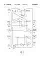
- FIG. 5is a detailed diagram of a bus arbiter shown in FIG. 2 according to present invention.
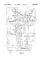
- FIG. 2shows a multi-processor interface 100 for connecting multiple processors, one at a time, to a memory shared by all the processors. All the processors need not have a wait, hold or ready input. Thus, unlike general micro-controllers or processors such as central processing units (CPUs), at least one of the processors may be of the type that does not have a wait or hold input, e.g., a digital signal processor (DSP).
- DSPdigital signal processor
- FIG. 2shows the multi-processor interface 100 which connects a CPU 105 and a DSP 110 to a shared single-port memory 115, such as a static random access memory (SRAM).
- SRAMstatic random access memory
- the multi-processor interface 100includes a bus arbiter 120 and arbitration logic 125.
- the arbitration logic 125selectively connects either the CPU 105 or the DSP 110 to the SRAM 115. As will be described, this selective connection to the memory 115 is achieved by multiplexers and buffers controlled by the bus arbiter 120. Four multiplexers selectively connect the CPU 105 or the DSP 110 to the memory 115. Further, four buffers allow for two way data transfer between the two processors 105, 110 and the memory 115.
- a chip select (CS) multiplexer 130selectively connects the CPUCS port 132 or the DSPCS port 134 to the memory CS port 136.
- the read/write (R/W) ports 142, 144 of the CPU and DSPare selectively connected one at a time to the memory R/W port 146 through a R/W multiplexer 140.
- the address ports 152, 154 of the CPU and DSPare selectively connected one at a time to the memory address port 156 through an address multiplexer 150.
- the CPU and DSP data ports 162, 164are selectively connected one at a time to the memory data-in port 166 and data-out port 168 through a data multiplexer 170 and four buffers 172, 174, 176, 178.
- Buffers 172, 176allow data flow from the CPU and DSP ports 162, 164 to the two inputs of the data multiplexer 170, which selectively connects one of the two processor data ports 162, 164 to the memory data-in port 166.
- buffers 174, 178selectively connect one at a time the CPU or DSP data ports 162, 164 to the memory data-out port 168.
- the multiplexers 130, 140, 150, 170are selected using a MUX control signal 180 from the bus arbiter 120 for connecting either the CPU 105 or the DSP 110 to the memory 115.
- a first state of the MUX control signal 180such as logic 0, connects the CPU 105 to the memory 115 while a second state, such as logic 1, connects the DSP 110 to the memory 115.
- a CPU data enable control signal 182 and a DSP data enable control signal 184cooperate to enable one of the buffers 174, 178 at any one time. This connects the memory data-out port 168 to the CPU or DSP data ports 162, 164.
- the bus arbiter 120has a CPU ready output port 190 which is connected to the CPU ready input port 192.
- a bus grant output port 194 of the bus arbiter 120is connected to a bus grant input port 196 of the DSP 110 which receives a BUS-GRANT signal as will be described.
- the bus arbiter 120also has CPU R/W and DSP R/W input ports 200, 201 which are connected to the CPU R/W and DSP R/W output ports 142, 144, respectively.
- a CPUCS complement input port 202 of the bus arbiter 120is connected to the CPUCS output port 132 of the CPU 105 through an inverter 203.
- a DSPCS complement input port 202' of the bus arbiter 120is connected to the DSPCS output ports 134 of the DSP 110 through an inverter 203'.
- the two inverters 203, 203', at the CPU and DSP chip select (CS) outputsare not needed in the case where CS complement signals are provided from the CPU 105 and DSP 110.
- a bus request (BUSREQ) input port 204 of the bus arbiter 120is connected to a BUSREQ output port 206 of the DSP 110.
- a DSP clock signalis also provided to the bus arbiter 120 at a DSPCLK input port 208 which is connected to the DSPCLK output port 209 of the DSP 110.
- the multi-processor interface 100allows for orderly and efficient memory access despite the DSP, which does not have a ready or halt/wait input and is continuously operating. Further, the CPU operation is only halted for a minimal duration. In particular, when the DSP 110 is already accessing the memory 115 and the CPU 105 requires memory access, then the CPU 105 is placed in a wait or hold state. This will be described in greater detail in connection with FIG. 4.
- the DSP 110continues operating to process data that does not require memory access, such as processing audio and/or video signals, until the CPU 105 is finished accessing the memory, in which case, the DSP 110 accesses the memory 115. This situation will be described in greater detail in connection with FIG. 3.
- the multi-processor interface 100allows the DSP 110, or any other processor lacking a ready input, to share the single port memory without being placed in a hold or wait state. This processor or DSP continues to operate instead of stopping operation or waiting for memory access.
- FIG. 3shows a timing diagram 210 of signals used for DSP memory access when the CPU 105 currently has memory access
- FIG. 4shows a timing diagram 220 of signals used for CPU memory access when the DSP 110 currently has memory access.
- the timing diagrams shown in FIGS. 3 and 4are achieved using the bus arbiter 120 as will be explained.
- the CPU 105outputs a high CPUCS signal when the CPU desires memory access, which in inverted by an inverter 203 to provide the bus arbiter 120 with a low 230 CPUCS complement signal.
- the CPUoperates and thus accesses the memory in response to the low 230 CPUCS complement signal so long as the CPU READY signal from the bus arbiter's CPURDY output port 190 is high.
- the READY signalis always high, as shown in FIG. 3 by reference numeral 232, indicating the CPU operation is never stopped, even when memory access is granted to the DSP 110, thus preventing efficiency reduction. This is because the DSP 110 is granted memory access when the CPU has finished accessing the memory, and there is no need to stop the CPU operation.
- a BUSREQ signal from the DSP bus request port 134 to the bus arbiter bus request port 204goes high 234 when the DSP desires memory access.
- FIG. 3shows the case where the DSP memory request or bus request occurs (BUSREQ goes high) during the CPU memory access time, i.e., when CPUCS complement is low 230 and READY is high 232.
- the low CPUCS complement 230prevents the bus arbiter 120 from granting a bus to the DSP 110 for connection to the memory 115.
- the bus arbiter 120grants a bus request to the DSP 110 when the CPU 105 finishes memory access.
- the rising edge 236 of the CPUCS complement signalwhich occurs when the CPU is finished accessing the memory, causes a BUSGNT signal to go high 238.
- the BUSGNT signalis provided from the bus arbiter's bus grant port 194 to the DSP's bus grant port 196.
- a DSPCS complement signalgoes low 242 (falling edge 244) which indicates that the DSP 110 has access the memory 115.
- the DSP memory accessis granted after the CPU finishes its memory access.
- DSP operationsare not halted, and the DSP continues its operations despite not being granted access to the memory.
- the DSPCS complement signalgoes high 243 (FIG. 3) and disables the DSP data buffer 178 (FIG. 2), as will be explained in connection with FIG. 5.
- the bus arbiter 120has a NOR gate 250 which receives the CPU chip select complement signal (CPUCS complement) as one input.
- An AND gate 255receives the DSP bus request signal BUSREQ at one input.
- Two registers, such as D flip-flops 260, 265,have their signal inputs connected to the output of the NOR and gates 250, 255, respectively.
- the flip-flops 260, 265are clocked by the DSPCLK signal received at the input port 201 of the bus arbiter 120.
- the true output of the first or CPU flip-flop 260provides a signal indicative of the CPU cycle, shown as CPUCYCLE, where the CPU has the bus and thus has access to the memory 115 (FIG. 2).
- the complement output of the CPU flip-flops 260is connected to the second input of the AND gate 255.
- the true output of the second or DSP flip-flop 265is the bus grant signal (BUSGNT), also referred to as the DSPCYCLE, since the DSP has the bus and thus has access to the memory 115 (FIG. 2).
- the complement output of the DSP flip-flops 265is the MUX signal 180, also shown in FIG. 2.
- the BUSGNT signal lineis connected to the second input of the NOR gate 250 as well as the first inputs of two NAND gates 270, 275.
- One of these two NAND gates 270has its other input connected to the CPUCS complement port 202 through an inverter 277, to receive the CPUCS true signal.
- the output of this NAND gate 270is the CPU ready signal CPURDY provided from output port 190 of the arbiter 120.
- the other NAND gate 275which receives the BUSGNT signal at one input, has another input connected to the arbiter's DSP read/write (R/W) port 201.
- a third input of the NAND gate 275is connected to the DSPCS complement port 202' through an inverter 277' to receive the DSPCS true signal.
- the output of this NAND gate 275is the DSP DATA ENABLE signal 184, also shown in FIG. 2.
- a high DSPCS complement signalshown in FIGS. 3 and 4, disables the DSP data buffer 178 (FIG. 2). This is readily ascertained from the NAND gate 275 of FIG. 5, which produces an enabling signal low only when all its inputs are high.
- a high DSPCS complement signal or a low DSPCS true signalwill cause the output of the NAND gate 275 (i.e., the DSP DATA ENABLE signal 184) to go high.
- the high DSP DATA ENABLE signal 184disables the DSP data buffer 178 after being inverted, as shown in FIG. 2 by the bubble at the DSP buffer 178.
- the bus arbiter 120also has a third NAND gate 280 with three inputs.
- the first input of this third NAND gate 280is connected to the MUX output port 180 and the second input is connected to the CPU R/W port 200 of the arbiter 120.
- the third input of the third NAND gate 280receives the CPUCS true signal from the inverter 277.
- the output of the third NAND gate 280is the CPU DATA ENABLE signal 182. Similar to the description in the previous paragraph concerning the high DSPCS complement signal, a high CPUCS complement signal disables the CPU data buffer 174 (FIG. 2).
- the high CPUCYCLE complementenables the AND gate 320 and passes the high BUSREQ to the DSP flip-flop 265, resulting in a high BUSGNT and a low MUX.
- the high BUSGNTis also referred to as the DSPCYCLE, where the DSP can access the memory.
- the high MUX signalenables the CPU DATA ENABLE NAND gate 280, providing a low output when the CPU R/W signal is high.
- this low CPU DATA ENABLE signalenables CPU buffer 174 after being inverted, as shown by the bubble at the CPU buffer 174. This provides a connection between the memory and the CPU.
- the low BUSGNTcauses a high output from the DSP DATA ENABLE NAND gate 184, thus producing a low signal to the DSP buffer 178 due to the bubble or inversion shown near the DSP buffer 178 in FIG. 2. This disables the DSP buffer 178 and prevents connection between the memory and the DSP.
- FIG. 4shows a timing diagram 220 for the case where the CPU 105 requests memory access while the DSP 110 is accessing the shared memory 115.
- the DSPoutputs to the bus arbiter a high 290 BUSREQ signal when the DSP desires memory access. If no collision exists, i.e., when the CPUCS complement is high 292 indicating the memory 115 (FIG. 2) is free and not being accessed by the CPU, then the bus arbiter 120 outputs a high 294 BUSGNT signal to the DSP in response to a BUSREQ, indicating the DSP has access to the memory.
- the rising edge 296 of the BUSREQ signalcauses the rising edge 298 of the BUSGNT, which in turn causes the falling edge 300 of the DSPCS.
- the low DSPCS signalindicates that the memory is being accessed by the DSP.
- the CPUCS complementgoes low 302.
- CPU operationis halted by the READY signal going low 304.
- the READY signalgoes high 308 and the CPU resumes its operation and begins memory access.
- the falling edge 310 of BUSGNTcauses the rising edge 312 of the READY signal shown in FIG. 4, also referred to as CPURDY in FIG. 5.
- the level changes of the CPURDY signalis readily seen in FIG. 5.
- CPURDY signalis low only when the two NAND gate 270 inputs, i.e., CPUCS and BUSGNT, are both high.
- the low BUSREQ signalcauses a low AND gate 255 output, thus a low BUSGNT signal.
- the high 292 CPUCS complement signalcauses a low output from the NOR gate 250, thus a low CPUCYCLE signal and a high input to the AND gate 255 which becomes enabled.
- the enabled AND gate 255passes the high BUSREQ and causes BUSGNT signal to go high 294.
- This high 294 BUSGNT signaldisables the NOR gate 250 and prevents its output to go high when the CPUCS complement goes low 302, thus preventing the CPUCYCLE signal from going high.
- the high 294 BUSGNT signalenables the NAND gate 270 thus allowing the high CPUCS to pass and provide the low 304 CPURDY signal.
- the low READY or CPURDY signalhalts CPU execution, or places the CPU in a wait state, thus preventing the CPU from accessing the memory.
- the CPURDY signal from the NAND gate 270goes high 308.
- the high CPURDY 308allows the CPU to resume operation and access the memory during time t 4 .
- the CPU memory accessoccurs during time t 4 since CPUCS complement is low 302 and BUSGNT is low 306, thus providing a high output from the NOR gate and a high CPUCYCLE, in addition to the high 308 CPURDY signal from the NAND gate 270.
- the low MUX signaldisables the CPU DATA ENABLE NAND gate 280, providing a high output irrelevant of the level of the CPU R/W signal.
- the high CPU DATA ENABLE 182disable the CPU buffer 174 and prevents connection between the memory and the CPU. This is due to the bubble or inversion shown near the DSP buffer 174 in FIG. 2.
- the high 294 BUSGNTenables the DSP DATA ENABLE NAND gate 275, passing the DSP R/W signal.
- the DSP DATA ENABLE signal 184is low.
- the low DSP DATA ENABLE signal 184enables DSP buffer 178 after being inverted, as shown by the bubble at the DSP buffer 178. This provides a connection between the memory and the DSP.
- the multi-processor interfaceis relatively simple in structure and does not require special algorithms or initialization software.
- the multi-processor interfaceis random access, which affords the flexibility to format data using software FIFO, or any appropriate sequence.
- the multi-processor interfaceis used in any device that requires more than one processor, such as telephones or displays, where a DSP is used for fast audio and/or video signal processing to provide acceptable audio and/or video signals, and a CPU which provides other control operations, such as call processing and user interface for wireless phones.
- a DSPis used for fast audio and/or video signal processing to provide acceptable audio and/or video signals
- a CPUwhich provides other control operations, such as call processing and user interface for wireless phones.
- the multi-processor interfacealleviates the need for a dual-ported memory, and allows a single-ported memory to be shared between two processors, where one of the processors does not have a wait or a hold signal such as a DSP, for example. Instead of dedicating a portion of a processing cycle to the microprocessor where the DSP is prevented from accessing the memory, and another portion to the DSP where microprocessor processing is halted, microprocessor executions are only halted when a collision occurs. Such collisions occur when one processor requests memory access while the other processor is already accessing the memory.
- the DSPoutputs the bus request signal BUSREQ when it requires access to the memory, and periodically checks for receipt of a bus acknowledge or grant signal BUSGNT. Meanwhile, the DSP continues its operation and accesses the memory upon receipt of the BUSGNT signal, which is provided by the bus arbiter when the memory is not being accessed by the CPU. Thus, the DSP operation is never halted.
- the CPU operationis halted or placed in a wait mode only when the CPU requires memory access while the DSP is accessing the memory. The CPU resumes operation and accesses the memory once the DSP finishes memory access.
- CPU operationis not halted when the DSP accesses memory. If there are no collisions, then the two processors operate continuously and access the shared memory whenever needed, through the bus arbiter, multiplexers and buffers, which allow the memory to be accessed by only one processor at a time.
Landscapes
- Engineering & Computer Science (AREA)
- Theoretical Computer Science (AREA)
- Physics & Mathematics (AREA)
- General Engineering & Computer Science (AREA)
- General Physics & Mathematics (AREA)
- Computer Hardware Design (AREA)
- Software Systems (AREA)
- Multi Processors (AREA)
Abstract
Description
Claims (15)
Priority Applications (1)
| Application Number | Priority Date | Filing Date | Title |
|---|---|---|---|
| US09/083,220US6163828A (en) | 1998-05-22 | 1998-05-22 | Methods and apparatus for providing multi-processor access to shared memory |
Applications Claiming Priority (1)
| Application Number | Priority Date | Filing Date | Title |
|---|---|---|---|
| US09/083,220US6163828A (en) | 1998-05-22 | 1998-05-22 | Methods and apparatus for providing multi-processor access to shared memory |
Publications (1)
| Publication Number | Publication Date |
|---|---|
| US6163828Atrue US6163828A (en) | 2000-12-19 |
Family
ID=22176949
Family Applications (1)
| Application Number | Title | Priority Date | Filing Date |
|---|---|---|---|
| US09/083,220Expired - LifetimeUS6163828A (en) | 1998-05-22 | 1998-05-22 | Methods and apparatus for providing multi-processor access to shared memory |
Country Status (1)
| Country | Link |
|---|---|
| US (1) | US6163828A (en) |
Cited By (14)
| Publication number | Priority date | Publication date | Assignee | Title |
|---|---|---|---|---|
| US20020004823A1 (en)* | 2000-07-06 | 2002-01-10 | Anderson Marquette John | Multi-processor system verification circuitry |
| US20040024929A1 (en)* | 2002-08-03 | 2004-02-05 | Chan Ming Hong | System and method for controlling communication on a signal bus |
| US20040064746A1 (en)* | 2001-01-31 | 2004-04-01 | Junichi Nishimoto | Data processing system and data processor |
| US20040107317A1 (en)* | 2002-11-28 | 2004-06-03 | Yong-Hyun Lee | Memory control apparatus and method for digital signal processing |
| US20060010264A1 (en)* | 2000-06-09 | 2006-01-12 | Rader Sheila M | Integrated processor platform supporting wireless handheld multi-media devices |
| US20060069881A1 (en)* | 2004-09-28 | 2006-03-30 | Toshiba Tec Kabushiki Kaisha | Shared memory access control apparatus |
| US20060146852A1 (en)* | 2004-12-30 | 2006-07-06 | Dinakar Munagala | Dataport and methods thereof |
| US7509391B1 (en)* | 1999-11-23 | 2009-03-24 | Texas Instruments Incorporated | Unified memory management system for multi processor heterogeneous architecture |
| CN100495371C (en)* | 2005-12-27 | 2009-06-03 | 威盛电子股份有限公司 | Computer system with clocked wait states |
| GB2458499A (en)* | 2008-03-20 | 2009-09-23 | Cambridge Silicon Radio Ltd | Sharing access to a data store by a host processor and a signal processor in a mobile phone |
| CN1866230B (en)* | 2005-08-11 | 2010-05-12 | 威盛电子股份有限公司 | Memory arbiter, processor system and memory arbitration method |
| US7761644B1 (en)* | 1999-08-21 | 2010-07-20 | St-Ericsson Sa | Memory sharing arrangement for an integrated multiprocessor system |
| US20110164833A1 (en)* | 2010-01-06 | 2011-07-07 | Samsung Electronics Co., Ltd. | Image processing apparatus and method |
| US20160299701A1 (en)* | 2015-04-13 | 2016-10-13 | Lsis Co., Ltd. | Access controlling method of dual port memory system |
Citations (10)
| Publication number | Priority date | Publication date | Assignee | Title |
|---|---|---|---|---|
| US4354227A (en)* | 1979-11-19 | 1982-10-12 | International Business Machines Corp. | Fixed resource allocation method and apparatus for multiprocessor systems having complementarily phased cycles |
| US4400771A (en)* | 1975-12-04 | 1983-08-23 | Tokyo Shibaura Electric Co., Ltd. | Multi-processor system with programmable memory-access priority control |
| US4549273A (en)* | 1982-12-10 | 1985-10-22 | Ael Microtel Limited | Memory access control circuit |
| US4737932A (en)* | 1984-06-05 | 1988-04-12 | Nec Corporation | Processor |
| EP0444711A2 (en)* | 1990-03-02 | 1991-09-04 | Fujitsu Limited | Bus control system in a multi-processor system |
| US5148112A (en)* | 1991-06-28 | 1992-09-15 | Digital Equipment Corporation | Efficient arbiter |
| US5175829A (en)* | 1988-10-25 | 1992-12-29 | Hewlett-Packard Company | Method and apparatus for bus lock during atomic computer operations |
| US5467461A (en)* | 1991-07-11 | 1995-11-14 | Nec Corporation | Multiprocessor computer system having bus control circuitry for transferring data between microcomputers |
| US5567900A (en)* | 1993-06-15 | 1996-10-22 | Yamaha Corporation | Electronic tone generator system with CPU and DSP |
| US5907862A (en)* | 1996-07-16 | 1999-05-25 | Standard Microsystems Corp. | Method and apparatus for the sharing of a memory device by multiple processors |
- 1998
- 1998-05-22USUS09/083,220patent/US6163828A/ennot_activeExpired - Lifetime
Patent Citations (10)
| Publication number | Priority date | Publication date | Assignee | Title |
|---|---|---|---|---|
| US4400771A (en)* | 1975-12-04 | 1983-08-23 | Tokyo Shibaura Electric Co., Ltd. | Multi-processor system with programmable memory-access priority control |
| US4354227A (en)* | 1979-11-19 | 1982-10-12 | International Business Machines Corp. | Fixed resource allocation method and apparatus for multiprocessor systems having complementarily phased cycles |
| US4549273A (en)* | 1982-12-10 | 1985-10-22 | Ael Microtel Limited | Memory access control circuit |
| US4737932A (en)* | 1984-06-05 | 1988-04-12 | Nec Corporation | Processor |
| US5175829A (en)* | 1988-10-25 | 1992-12-29 | Hewlett-Packard Company | Method and apparatus for bus lock during atomic computer operations |
| EP0444711A2 (en)* | 1990-03-02 | 1991-09-04 | Fujitsu Limited | Bus control system in a multi-processor system |
| US5148112A (en)* | 1991-06-28 | 1992-09-15 | Digital Equipment Corporation | Efficient arbiter |
| US5467461A (en)* | 1991-07-11 | 1995-11-14 | Nec Corporation | Multiprocessor computer system having bus control circuitry for transferring data between microcomputers |
| US5567900A (en)* | 1993-06-15 | 1996-10-22 | Yamaha Corporation | Electronic tone generator system with CPU and DSP |
| US5907862A (en)* | 1996-07-16 | 1999-05-25 | Standard Microsystems Corp. | Method and apparatus for the sharing of a memory device by multiple processors |
Non-Patent Citations (6)
| Title |
|---|
| By Alan Clements, "Microcomputer Design and Construction" Prentice Hall International, pp. 378-385. |
| By Alan Clements, "Microcomputer Design andConstruction" Prentice Hall International, pp. 375-378. |
| By Alan Clements, Microcomputer Design and Construction Prentice Hall International, pp. 378 385.* |
| By Alan Clements, Microcomputer Design andConstruction Prentice Hall International, pp. 375 378.* |
| By Thomas L. Harman, The Motorola MC68000 Microprocessor Family: Assembly Language, Interface Design, and System Design. Published Prentice Hall, Englewood Cliffs, NJ, pp. 332 336, 360 364.* |
| By Thomas L. Harman, The Motorola MC68000 Microprocessor Family: Assembly Language, Interface Design, and System Design. Published Prentice Hall, Englewood Cliffs, NJ, pp. 332-336, 360-364. |
Cited By (36)
| Publication number | Priority date | Publication date | Assignee | Title |
|---|---|---|---|---|
| US7761644B1 (en)* | 1999-08-21 | 2010-07-20 | St-Ericsson Sa | Memory sharing arrangement for an integrated multiprocessor system |
| US7509391B1 (en)* | 1999-11-23 | 2009-03-24 | Texas Instruments Incorporated | Unified memory management system for multi processor heterogeneous architecture |
| US20060010264A1 (en)* | 2000-06-09 | 2006-01-12 | Rader Sheila M | Integrated processor platform supporting wireless handheld multi-media devices |
| US7281066B2 (en)* | 2000-06-09 | 2007-10-09 | Motorola, Inc. | Memory access system including support for multiple bus widths |
| US20020004823A1 (en)* | 2000-07-06 | 2002-01-10 | Anderson Marquette John | Multi-processor system verification circuitry |
| US7469273B2 (en)* | 2000-07-06 | 2008-12-23 | Texas Instruments Incorporated | Multi-processor system verification circuitry |
| US8244926B2 (en) | 2001-01-31 | 2012-08-14 | Renesas Electronics Corporation | Data processing system and data processor |
| US7401165B2 (en) | 2001-01-31 | 2008-07-15 | Renesas Technology Corporation | Data processing system and data processor |
| US7975077B2 (en) | 2001-01-31 | 2011-07-05 | Renesas Electronics Corporation | Data processing system and data processor |
| US9069911B2 (en) | 2001-01-31 | 2015-06-30 | Renesas Electronics Corporation | Data processing system and data processor |
| US20110131349A1 (en)* | 2001-01-31 | 2011-06-02 | Renesas Electronics Corporation | Data processing system and data processor |
| US20050273526A1 (en)* | 2001-01-31 | 2005-12-08 | Junichi Nishimoto | Data processing system and data processor |
| US7401163B2 (en)* | 2001-01-31 | 2008-07-15 | Renesas Technology Corporation | Data processing system and data processor |
| US7725616B2 (en) | 2001-01-31 | 2010-05-25 | Renesas Technology Corp. | Data processing system and data processor |
| US20080250187A1 (en)* | 2001-01-31 | 2008-10-09 | Junichi Nishimoto | Data processing system and data processor |
| US8595388B2 (en) | 2001-01-31 | 2013-11-26 | Renesas Electronics Corporation | Data processing system and data processor |
| US20040064746A1 (en)* | 2001-01-31 | 2004-04-01 | Junichi Nishimoto | Data processing system and data processor |
| US8812750B2 (en) | 2001-01-31 | 2014-08-19 | Renesas Electronics Corporation | Data processing system and data processor |
| US20090235007A1 (en)* | 2001-01-31 | 2009-09-17 | Renesas Technology Corp. | Data processing system and data processor |
| WO2004013896A3 (en)* | 2002-08-03 | 2004-04-01 | Ess Technology Inc | System and method for controlling communication on a signal bus |
| US20040024929A1 (en)* | 2002-08-03 | 2004-02-05 | Chan Ming Hong | System and method for controlling communication on a signal bus |
| US6990537B2 (en) | 2002-08-03 | 2006-01-24 | Ess Technology, Inc. | System and method for controlling multi-component communications via a bus by causing components to enter and exit a high-impedance state |
| US20040107317A1 (en)* | 2002-11-28 | 2004-06-03 | Yong-Hyun Lee | Memory control apparatus and method for digital signal processing |
| US7594045B2 (en) | 2002-11-28 | 2009-09-22 | Samsung Electronics Co., Ltd. | Memory control apparatus for digital signal processing |
| US20060230194A1 (en)* | 2002-11-28 | 2006-10-12 | Yong-Hyun Lee | Memory control apparatus and method for digital signal processing |
| US20060069881A1 (en)* | 2004-09-28 | 2006-03-30 | Toshiba Tec Kabushiki Kaisha | Shared memory access control apparatus |
| US8279886B2 (en)* | 2004-12-30 | 2012-10-02 | Intel Corporation | Dataport and methods thereof |
| US8902915B2 (en) | 2004-12-30 | 2014-12-02 | Intel Corporation | Dataport and methods thereof |
| US20060146852A1 (en)* | 2004-12-30 | 2006-07-06 | Dinakar Munagala | Dataport and methods thereof |
| CN1866230B (en)* | 2005-08-11 | 2010-05-12 | 威盛电子股份有限公司 | Memory arbiter, processor system and memory arbitration method |
| CN100495371C (en)* | 2005-12-27 | 2009-06-03 | 威盛电子股份有限公司 | Computer system with clocked wait states |
| GB2458499A (en)* | 2008-03-20 | 2009-09-23 | Cambridge Silicon Radio Ltd | Sharing access to a data store by a host processor and a signal processor in a mobile phone |
| US20110164833A1 (en)* | 2010-01-06 | 2011-07-07 | Samsung Electronics Co., Ltd. | Image processing apparatus and method |
| US9053521B2 (en)* | 2010-01-06 | 2015-06-09 | Samsung Electronics Co., Ltd. | Image processing apparatus and method |
| US20160299701A1 (en)* | 2015-04-13 | 2016-10-13 | Lsis Co., Ltd. | Access controlling method of dual port memory system |
| US9766821B2 (en)* | 2015-04-13 | 2017-09-19 | Lsis Co., Ltd. | Access controlling method of dual port memory system |
Similar Documents
| Publication | Publication Date | Title |
|---|---|---|
| US5398211A (en) | Structure and method for providing prioritized arbitration in a dual port memory | |
| US4641266A (en) | Access-arbitration scheme | |
| EP0166272B1 (en) | Processor bus access | |
| US6163828A (en) | Methods and apparatus for providing multi-processor access to shared memory | |
| US6480929B1 (en) | Pseudo-concurrency between a volatile memory and a non-volatile memory on a same data bus | |
| US5555425A (en) | Multi-master bus arbitration system in which the address and data lines of the bus may be separately granted to individual masters | |
| US6272582B1 (en) | PCI-PCI bridge allowing controlling of a plurality of PCI agents including a VGA device | |
| US5943500A (en) | Long latency interrupt handling and input/output write posting | |
| US6148357A (en) | Integrated CPU and memory controller utilizing a communication link having isochronous and asynchronous priority modes | |
| US5954809A (en) | Circuit for handling distributed arbitration in a computer system having multiple arbiters | |
| US7650453B2 (en) | Information processing apparatus having multiple processing units sharing multiple resources | |
| US5041962A (en) | Computer system with means for regulating effective processing rates | |
| US5717873A (en) | Deadlock avoidance mechanism and method for multiple bus topology | |
| US5426737A (en) | Direct memory access for data transfer within an I/O device | |
| JPH04268938A (en) | Data processing apparatus and memory controller | |
| JPH07105146A (en) | Shared memory device | |
| US20020059486A1 (en) | Shared component clock protection for multicore DSP device | |
| US20050160188A1 (en) | Method and apparatus to manage memory access requests | |
| US5353416A (en) | CPU lock logic for corrected operation with a posted write array | |
| US6212589B1 (en) | System resource arbitration mechanism for a host bridge | |
| US6490638B1 (en) | General purpose bus with programmable timing | |
| JP3504266B2 (en) | Enhanced parallel port | |
| US7006521B2 (en) | External bus arbitration technique for multicore DSP device | |
| US6442632B1 (en) | System resource arbitration mechanism for a host bridge | |
| US5960180A (en) | Host adapter integrated circuit having autoaccess pause |
Legal Events
| Date | Code | Title | Description |
|---|---|---|---|
| AS | Assignment | Owner name:PHILIPS CONSUMER COMMUNICATIONS, L.P., NEW YORK Free format text:ASSIGNMENT OF ASSIGNORS INTEREST;ASSIGNORS:LANDI, JOSEPH;FERRERAS, THOMAS;FATHI, MEHRDAD;REEL/FRAME:009344/0706;SIGNING DATES FROM 19980625 TO 19980701 | |
| FEPP | Fee payment procedure | Free format text:PAYOR NUMBER ASSIGNED (ORIGINAL EVENT CODE: ASPN); ENTITY STATUS OF PATENT OWNER: LARGE ENTITY | |
| STCF | Information on status: patent grant | Free format text:PATENTED CASE | |
| FEPP | Fee payment procedure | Free format text:PAYER NUMBER DE-ASSIGNED (ORIGINAL EVENT CODE: RMPN); ENTITY STATUS OF PATENT OWNER: LARGE ENTITY Free format text:PAYOR NUMBER ASSIGNED (ORIGINAL EVENT CODE: ASPN); ENTITY STATUS OF PATENT OWNER: LARGE ENTITY | |
| FPAY | Fee payment | Year of fee payment:4 | |
| FPAY | Fee payment | Year of fee payment:8 | |
| FPAY | Fee payment | Year of fee payment:12 | |
| AS | Assignment | Owner name:PROVENANCE ASSET GROUP LLC, CONNECTICUT Free format text:ASSIGNMENT OF ASSIGNORS INTEREST;ASSIGNORS:NOKIA TECHNOLOGIES OY;NOKIA SOLUTIONS AND NETWORKS BV;ALCATEL LUCENT SAS;REEL/FRAME:043877/0001 Effective date:20170912 Owner name:NOKIA USA INC., CALIFORNIA Free format text:SECURITY INTEREST;ASSIGNORS:PROVENANCE ASSET GROUP HOLDINGS, LLC;PROVENANCE ASSET GROUP LLC;REEL/FRAME:043879/0001 Effective date:20170913 Owner name:CORTLAND CAPITAL MARKET SERVICES, LLC, ILLINOIS Free format text:SECURITY INTEREST;ASSIGNORS:PROVENANCE ASSET GROUP HOLDINGS, LLC;PROVENANCE ASSET GROUP, LLC;REEL/FRAME:043967/0001 Effective date:20170913 | |
| AS | Assignment | Owner name:NOKIA US HOLDINGS INC., NEW JERSEY Free format text:ASSIGNMENT AND ASSUMPTION AGREEMENT;ASSIGNOR:NOKIA USA INC.;REEL/FRAME:048370/0682 Effective date:20181220 | |
| AS | Assignment | Owner name:PROVENANCE ASSET GROUP LLC, CONNECTICUT Free format text:RELEASE BY SECURED PARTY;ASSIGNOR:CORTLAND CAPITAL MARKETS SERVICES LLC;REEL/FRAME:058983/0104 Effective date:20211101 Owner name:PROVENANCE ASSET GROUP HOLDINGS LLC, CONNECTICUT Free format text:RELEASE BY SECURED PARTY;ASSIGNOR:CORTLAND CAPITAL MARKETS SERVICES LLC;REEL/FRAME:058983/0104 Effective date:20211101 Owner name:PROVENANCE ASSET GROUP LLC, CONNECTICUT Free format text:RELEASE BY SECURED PARTY;ASSIGNOR:NOKIA US HOLDINGS INC.;REEL/FRAME:058363/0723 Effective date:20211129 Owner name:PROVENANCE ASSET GROUP HOLDINGS LLC, CONNECTICUT Free format text:RELEASE BY SECURED PARTY;ASSIGNOR:NOKIA US HOLDINGS INC.;REEL/FRAME:058363/0723 Effective date:20211129 | |
| AS | Assignment | Owner name:RPX CORPORATION, CALIFORNIA Free format text:ASSIGNMENT OF ASSIGNORS INTEREST;ASSIGNOR:PROVENANCE ASSET GROUP LLC;REEL/FRAME:059352/0001 Effective date:20211129 |