US6163708A - Closed-loop power control method - Google Patents
Closed-loop power control methodDownload PDFInfo
- Publication number
- US6163708A US6163708AUS09/224,653US22465398AUS6163708AUS 6163708 AUS6163708 AUS 6163708AUS 22465398 AUS22465398 AUS 22465398AUS 6163708 AUS6163708 AUS 6163708A
- Authority
- US
- United States
- Prior art keywords
- signal
- power control
- dac
- reference signal
- communication
- Prior art date
- Legal status (The legal status is an assumption and is not a legal conclusion. Google has not performed a legal analysis and makes no representation as to the accuracy of the status listed.)
- Expired - Lifetime
Links
- 238000000034methodMethods0.000titleclaimsdescription16
- 238000004891communicationMethods0.000claimsabstractdescription68
- 230000008859changeEffects0.000claimsdescription4
- 238000001514detection methodMethods0.000abstractdescription2
- 230000010267cellular communicationEffects0.000description5
- 238000010586diagramMethods0.000description4
- 238000013459approachMethods0.000description1
- 230000001413cellular effectEffects0.000description1
- 238000010276constructionMethods0.000description1
- 230000001276controlling effectEffects0.000description1
- 238000007796conventional methodMethods0.000description1
- 238000013461designMethods0.000description1
- 238000005516engineering processMethods0.000description1
- 239000000284extractSubstances0.000description1
- 230000005669field effectEffects0.000description1
- 229910044991metal oxideInorganic materials0.000description1
- 150000004706metal oxidesChemical class0.000description1
- 230000010363phase shiftEffects0.000description1
- 230000008569processEffects0.000description1
- 230000001105regulatory effectEffects0.000description1
- 230000004044responseEffects0.000description1
- 239000004065semiconductorSubstances0.000description1
- 238000001228spectrumMethods0.000description1
Images


Classifications
- H—ELECTRICITY
- H04—ELECTRIC COMMUNICATION TECHNIQUE
- H04W—WIRELESS COMMUNICATION NETWORKS
- H04W52/00—Power management, e.g. Transmission Power Control [TPC] or power classes
- H04W52/04—Transmission power control [TPC]
- H04W52/18—TPC being performed according to specific parameters
- H04W52/22—TPC being performed according to specific parameters taking into account previous information or commands
- H04W52/221—TPC being performed according to specific parameters taking into account previous information or commands using past power control commands
- H—ELECTRICITY
- H04—ELECTRIC COMMUNICATION TECHNIQUE
- H04W—WIRELESS COMMUNICATION NETWORKS
- H04W52/00—Power management, e.g. Transmission Power Control [TPC] or power classes
- H04W52/04—Transmission power control [TPC]
- H04W52/30—Transmission power control [TPC] using constraints in the total amount of available transmission power
- H04W52/36—Transmission power control [TPC] using constraints in the total amount of available transmission power with a discrete range or set of values, e.g. step size, ramping or offsets
- H—ELECTRICITY
- H04—ELECTRIC COMMUNICATION TECHNIQUE
- H04W—WIRELESS COMMUNICATION NETWORKS
- H04W52/00—Power management, e.g. Transmission Power Control [TPC] or power classes
- H04W52/04—Transmission power control [TPC]
- H04W52/52—Transmission power control [TPC] using AGC [Automatic Gain Control] circuits or amplifiers
Definitions
- the present inventiondescribes a power control method used in wireless communications.
- the methodutilizes a switched-current, exponential digital-to-analog converter to alter the gain of a transmitter according to received power control bits.
- the approachis simple and suitable for fast power control.
- a radio communication channelextends between a sending station and a receiving station.
- the radio channelis defined upon a portion of the electromagnetic spectrum. This communication link between the sending and receiving stations is wireless and does not require a wire line connection. Communication can thereby be untethered.
- a cellular communication systemis exemplary of a wireless, multi-user radio communication system.
- several fixed-site base stationsare installed to cover a geographical area.
- the same frequenciescan be re-used at different locations throughout the geographical area.
- Power controlis at the core of cellular system design.
- IS-95 and IS-98are cellular communication standards which rely on CDMA (code division multiple access) communication techniques.
- CDMAcode division multiple access
- power control informationis generated and transmitted by the network infrastructure to a mobile handset.
- the control informationis sent in the form of power control bits.
- the control bitsadjust the level of transmitted power.
- the closed loop power control schemeaugments open loop power control methods. These schemes use approximation techniques based on the assumption that both the downlink and uplink channels experience similar path losses. Open loop power control schemes are generally slower and less accurate than closed loop power control schemes. Closed loop power control schemes are typically more complex, but, necessary to ensure that the transmitted signals are in compliance with the requirements set forth in the aforementioned standards. Interim standards IS-95 and IS-98 utilize a 800 Hz power control loop. Future standards will exploit faster power control schemes. Future standards will also occupy a wider bandwidth and require finer power control.
- the present inventionadvantageously provides a method for fast closed loop gain control.
- gain controlis directed by power control bits.
- the power control bitscause an increase or decrease of the power level of the transmitted signal generated by the mobile handset.
- Closed-loop power controlis provided by a simple circuit, which exhibits high levels of differential linearity.
- An embodiment of the present inventionis advantageous in a communication device that communicates data at high data rates.
- power control bitsare transmitted upon a downlink channel by network infrastructure to the mobile station every 1.25 milliseconds.
- the power control bitsdirect the mobile station to increase or to decrease the power level of uplink signals transmitted by the mobile station. That is to say, each power control bit increments or decrements the gain of the transmitter amplifier.
- Interim standard IS-95Bcalls for the resolution of the gain increase or decrease to be selectable as either 0.25 dB, 0.5 dB, or 1.0 dB.
- a mobile station that supports an IS-95B systemrequires this selectivity, which is provided by the present invention.
- Datais formatted into successive frames in the interim standard IS-95 system. Sixteen power control bits are associated with each frame of data. Up to sixteen increments or decrements of the gain can occur each frame. When the resolution is 1.0 dB, a maximum range of 16 dB of gain change can be accomplished.
- power control bits received at the receiver portion of the mobile handsetare provided as digital inputs to a switched-current, exponential DAC (digital-to-analog converter).
- the switched-current exponential DACgenerates an analog output signal that is step-wise exponentially related to its previous value.
- the analog output of the DACis applied to the transmitter to control its gain.
- the output signal of the DACis used as a reference input to baseband digital-to-analog converters.
- the baseband digital-to-analog convertersgenerate signals which are applied to an I/Q modulator.
- a methodfor controlling the gain level of a communication signal.
- the mobile handsetcan receive power control bits which indicate at least relative power levels of the signal to be transmitted.
- An exponential converteris coupled to receive each successive power control bit received.
- the exponential convertergenerates an output signal which is step-wise exponentially related to each successive power control bit.
- Communication signal DACsgenerate analog signals that represent the baseband information plus the output of the step-wise exponential power control DAC.
- FIG. 1illustrates a functional block diagram of an exemplary communication system in which an embodiment of the present invention is operable.
- FIG. 2illustrates a timing diagram showing the formatting scheme pursuant to which power control bits are transmitted upon a downlink channel to the mobile station forming a portion of the communication system shown in FIG. 1.
- FIG. 3illustrates a functional block diagram of the mobile station forming a portion of the communication system shown in FIG. 1.
- FIG. 4illustrates a functional block diagram of an embodiment of the present invention, here forming a portion of the mobile station shown in FIG. 3.
- FIG. 5illustrates a circuit schematic of the switched current, exponential DAC (digital-to-analog converter) of the apparatus of an embodiment of the present invention.
- FIG. 6illustrates a circuit schematic of a portion of the switched current, exponential DAC shown in FIG. 5, of a further embodiment of the present invention.
- an exemplary communication systemshown generally at 10, permits two-way communication between a base station 12, and a mobile station 14.
- the exemplary communication system 10 shown in the Figureis representative of a CDMA cellular communication system, for example, a system as defined in the IS-95 interim standard developed by the EIA/TIA.
- An embodiment of the present inventionis also operable in other types of communication systems.
- Communication signals transmitted over the air interface between the network infrastructure and the mobile stationmust be at appropriate power levels to ensure that transmitted signals are reliably received.
- power control bitsare transmitted by the network infrastructure to a mobile station to control the power level of the mobile station transmitter.
- the line 24is representative of a downlink channel upon which signals generated by the network infrastructure are transmitted to the mobile station 14.
- the line 26is representative of an uplink channel upon which uplink signals generated by the mobile station are transmitted to the network infrastructure.
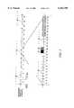
- FIG. 2illustrates the formatting scheme for the downlink traffic channel of IS-95.
- each traffic frameis divided into groups of sixteen power control groups 32. Sixteen of such power control groups 32, here numbered 0-15 are illustrated in the Figure.
- Each of the power control groups 32is further formatted into twenty-four modulation symbols 34.
- the formattingis represented by the expansion of the seventh power control group 32. Power control bits, of which the bits 42 and 44 are exemplary, replace pseudo-randomly two of the first sixteen symbols.
- FIG. 3illustrates the mobile station, shown previously in FIG. 1, here operable pursuant to an embodiment of the present invention.
- the mobile stationis selectively tuned to the desired frequency channel.
- Electromagnetic signalsare detected by the antenna transducer 52, converted into electrical form, and provided to a down converter 54.
- the down converter 54translates the received signals to IF.
- the demodulator 56converts the IF signal to baseband I- and Q-signals which are applied to ADCs (analog-to-digital converters) 58.
- the converters 58convert the signals to digital form and provide such digitized signals to a rake receiver 62.
- the rake receiver 62includes a plurality of dynamically-assigned fingers (not shown).
- the rake receiver 62further includes a symbol combiner 66 which combines symbols from the various fingers of the rake receiver.
- Resultant symbols formed by the symbol combinerare provided to a decoder 72 which decodes the symbols provided thereto.
- the decoder 72generates decoded signals which are provided to a data sink 74, such as a speaker element.
- the mobile station 14further includes a controller 76 which extracts power control bits.
- the power control bits extracted by the controller 76are provided as a digital input to a switched-current exponential DAC (digital-to-analog converter) 82.
- the switched-current exponential DAC 82generates an analog output signal on the line 84 indicating power control bit values.
- the analog output signal of DAC 82 on line 84is coupled to control I and Q DACs (digital-to-analog converters) 86, and thereby adjust the amplitude of the analog output signals produced by the converters 86.
- These DACs 86receive digital encoded signals generated by an encoder 88 and originated from a data source 92.
- the DACs 86generate analog output signals representative of the analog encoded signals and provides these signals to the input of an I/Q modulator 96.
- the modulator 96generates modulated signals which are provided to a variable gain amplifier 98.
- the amplifier 98amplifies the signals provided and provides amplified signals to an up-converter 102.
- the gain of the variable gain amplifier 98is determined by an open-loop gain control process.
- the up-converter 102generates up-converted signals which are provided to a power amplifier 104 to be amplified. Amplified signals generated by the power amplifier 104 are provided to the antenna transducer 52 to be radiated.
- FIG. 4illustrates portions of the mobile station 10 shown in FIG. 3. More particularly, the switched-current exponential DAC 82, the I and Q DACs 86, and the I/Q modulator 96 are again shown.
- the extracted power control bitsare provided as digital inputs to the switched-current exponential DAC 82.
- This DAC 82generates analog signals on the line 84 which are provided to control the I and Q digital DACs 86.
- the I and Q converters 86are coupled to receive I and Q signals from the encoder 88 (shown in FIG. 3).
- Analog signals generated by the converters 86are filtered by filters 106 and 108, here represented to form portions of the I/Q modulator 96. Filtered signals generated by the filters 106 and 108 are provided to input terminals of mixer elements 112 and 114, respectively. Oscillating signals generated by an oscillator 116 are also provided to the mixers 112 and 114. The oscillating signal provided to the mixer circuit 114 is phase-shifted by a ninety degree phase shift by a phase shifter 118. Mixed signals generated by the mixer circuits 112 and 114 are combined together and thereafter applied to the variable gain amplifier 98 (shown in FIG. 3).
- FIG. 5illustrates the switched-current exponential DAC 82 of an embodiment of the present invention in greater detail.
- the DAC 82is formed of MOSFETs (metal oxide semiconductor field effect transistors).
- MOSFETsmetal oxide semiconductor field effect transistors
- the DAC 82can analogously be formed of other types of devices.
- the drain current, I D , generated at the drain electrode of a MOSFET deviceis defined by the following equation: ##EQU1## Wherein: ⁇ s is the surface mobility;
- C oxis the oxide capacitance
- Wis the width of the transistor device
- Lis the length of the transistor device
- V gsis the gate-to-source voltage of the transistor device
- V Tis the threshold voltage of the transistor device.
- a gate-source capacitanceis also associated with the MOS transistor.
- An applied gate-source voltage to the transistor devicecharges such capacitance. When the applied voltage is removed, the drain current is unaffected, and the transistor device functions as an analog memory device.
- the DAC 82includes a plurality of N-channel transistor devices, here designated N1, N2, N3, N4 and N5.
- the DACfurther includes a plurality of P-channel transistor devices, here designated by P1, P2, P3, P4 and P5.
- the DAC 82further includes a plurality of switch elements, here designated by S1, S2, S3, S4, S5, S6, and S7.
- a bias sourceis applied to the DAC 82 on the line 122.
- Source electrodes of each of the P-channel transistors P1-P5are coupled to the line 122.
- the DAC 82further includes a second line 124, here coupled to a common potential, to which each source of the N-channel transistors, transistors N1-N6 are coupled.
- Opening and closing of the switches S1-S7describe the operation of the switched current exponential DAC 82.
- the switches S1 and S3are closed.
- the reference currentis applied to the source of transistor N1 and transistor N1 develops a gate-source voltage corresponding to the level of the drain current applied. All of the current is applied to transistor N1 as the gate current of an MOS transistor is negligible, ideally zero value.
- switch S3is opened, with the gate-source voltage stored by the transistor N1.
- Switch S1is then opened while switch S2 is closed.
- the transistor N1 and N5form a current mirror, and the drain current of the transistor N1 is equal to the drain current of the transistor N5.
- the transistors P4 and P5also form a current mirror and the drain currents of the transistors P4 and P5 are also equal to one another.
- the transistors N1, N5, P4 and P5together form a loop, each with equal current levels.
- the transistors N1 and N4also form a current mirror.
- the transistor N4is sized differently than that of the transistor N1 and, assuming the transistors N1 and N4 to be of equal lengths, the drain current, I D4 of the transistor N4 is defined by the following equation: ##EQU2## Wherein: I D1 is the drain current of the transistor N1;
- W 4is the width of the transistor N4.
- W 1is the width of the transistor N1.
- the ratio of the widths of the transistors N4 and N1are selected to effectuate a selected control step, such as 1 dB, 0.5 dB, or 0.25 dB.
- Opening and closing of the switches S4 and S5are made to effectuate decrement and increment commands of the control steps, respectively.
- the switch S5is closed together with the switches S6 and S7.
- the drain current of the transistor N4is mirrored by the transistors P2 and P3.
- the drain current of the transistor P2is thereby caused to be added to the drain current of transistor P4, thereby increasing the drain current of the transistor N1 from its original value.
- the gate-source capacitances of the transistors P2 and P4are also caused to be charged.
- the switches S6 and S7are then opened and a switch S3 is then closed.
- the gate-source voltage of the transistor N1increases to reflect the new, higher value of the drain current.
- the transistor N4then operates at the new current level.
- two non-overlapping clock pulsesare required.
- the switch S3is opened and closed pursuant to a first clock, and the switches S4-S7 are operated with a second clock. Appropriate clocking of the switches also minimizes leakage of the MOS transistors forming the DAC 82.
- the current level generated at the output line 84is governed by the following equation:
- N10 dB/20 ;
- iis the previous current level generated by the DAC 82.
- a current-step incrementis achieved by adding a fraction of the original value, i, to itself. And, conversely, a decrement is achieved by reducing the original value, i, by a similar fraction.
- the fractional changeis related to the control-step size, determined by the ratio of the width of the transistors N4 and N1.
- the fractional decrement of current levelsis -2.84%, and the fractional increment of current levels is +2.92%.
- the control step sizeis 0.5 dB, the fractional decrement is -5.59%, and the fractional increment in current levels is +5.93%.
- the control step sizeis 1.0 dB, the fractional decrement is -10.87%, and the fractional increment of current levels is +12.2%.
- successive current level increments or decrementsare caused to be generated on the line 84 responsive to detection at the mobile station of the power control bits. For instance, for eight successive logic Hi power control bits, with the control steps set at 1.0 dB, an increase of 8 dB power level is caused to be effectuated.
- FIG. 6illustrates the transistor N4, forming a portion of the DAC 82 shown in FIG. 5 of an embodiment of the present invention, together with the transistor N1 and transistor P3.
- the transistor N4is selected between one of three transistors, transistor 132, transistor 134, or transistor 136.
- Each of the transistors 132, 134, and 136are coupled in parallel to one another through a switch 142.
- Each ofthe transistors 132, 134, and 136is differently sized, creating a different width ratio with the transistor N1.
- the control step sizeis selected through this switch 142 and a manner is provided to control the power level of the transmitted signal.
- the circuit 82is of simple construction, capable of quick response to power control commands.
Landscapes
- Engineering & Computer Science (AREA)
- Computer Networks & Wireless Communication (AREA)
- Signal Processing (AREA)
- Transmitters (AREA)
- Transceivers (AREA)
- Mobile Radio Communication Systems (AREA)
Abstract
Description
i=Ni
Claims (20)
i=Ni
N=10.sup.(control step/20).
Priority Applications (6)
| Application Number | Priority Date | Filing Date | Title |
|---|---|---|---|
| US09/224,653US6163708A (en) | 1998-12-31 | 1998-12-31 | Closed-loop power control method |
| DE69920751TDE69920751T2 (en) | 1998-12-31 | 1999-12-28 | POWER CONTROL PROCEDURE WITH CLOSED REGULATORY CIRCUIT |
| EP99966682AEP1142290B1 (en) | 1998-12-31 | 1999-12-28 | Closed-loop power control method |
| PCT/US1999/031031WO2000039992A1 (en) | 1998-12-31 | 1999-12-28 | Closed-loop power control method |
| JP2000591778AJP2002534850A (en) | 1998-12-31 | 1999-12-28 | Closed loop power control method |
| AU22182/00AAU2218200A (en) | 1998-12-31 | 1999-12-28 | Closed-loop power control method |
Applications Claiming Priority (1)
| Application Number | Priority Date | Filing Date | Title |
|---|---|---|---|
| US09/224,653US6163708A (en) | 1998-12-31 | 1998-12-31 | Closed-loop power control method |
Publications (1)
| Publication Number | Publication Date |
|---|---|
| US6163708Atrue US6163708A (en) | 2000-12-19 |
Family
ID=22841578
Family Applications (1)
| Application Number | Title | Priority Date | Filing Date |
|---|---|---|---|
| US09/224,653Expired - LifetimeUS6163708A (en) | 1998-12-31 | 1998-12-31 | Closed-loop power control method |
Country Status (6)
| Country | Link |
|---|---|
| US (1) | US6163708A (en) |
| EP (1) | EP1142290B1 (en) |
| JP (1) | JP2002534850A (en) |
| AU (1) | AU2218200A (en) |
| DE (1) | DE69920751T2 (en) |
| WO (1) | WO2000039992A1 (en) |
Cited By (18)
| Publication number | Priority date | Publication date | Assignee | Title |
|---|---|---|---|---|
| WO2001039452A1 (en)* | 1999-11-29 | 2001-05-31 | Golden Bridge Technology, Inc. | Closed loop power control for common downlink transport channels |
| US6418321B1 (en)* | 1998-01-05 | 2002-07-09 | Oki Electric Industry Co., Ltd. | Transmission power controller |
| WO2002060088A1 (en)* | 2000-11-02 | 2002-08-01 | Conexant Systems, Inc. | Continuous closed-loop power control system including modulation injection in a wireless transceiver power amplifier |
| US6463296B1 (en)* | 1999-02-16 | 2002-10-08 | Telefonaktiebolaget L M Ericsson (Publ) | Power control in a CDMA mobile communications system |
| US20020173331A1 (en)* | 2001-05-19 | 2002-11-21 | Lg Electronics Inc. | Enhanced closed-loop power control method |
| US20030137958A1 (en)* | 1998-03-26 | 2003-07-24 | Mitsubishi Denki Kabushiki Kaisha | Spread spectrum communication device and spread spectrum communication method |
| US6606341B1 (en) | 1999-03-22 | 2003-08-12 | Golden Bridge Technology, Inc. | Common packet channel with firm handoff |
| US6717981B1 (en)* | 1999-12-14 | 2004-04-06 | Koninklijke Philips Electronics N.V. | Transmitter image suppression in TDD transceivers |
| US6757319B1 (en) | 1999-11-29 | 2004-06-29 | Golden Bridge Technology Inc. | Closed loop power control for common downlink transport channels |
| US20040132470A1 (en)* | 2001-05-04 | 2004-07-08 | Xavier Checoury | Amplitude- and frequency- or phase-modulated radio frequency signal generator and the transmitter incorporating same |
| US6914889B1 (en)* | 1998-12-08 | 2005-07-05 | Lucent Technologies Inc. | Variable rate forward power control for multichannel applications |
| US20070014381A1 (en)* | 2005-07-13 | 2007-01-18 | Dmitriy Rozenblit | Polar loop radio frequency (RF) transmitter having increased dynamic range amplitude control |
| WO2007018696A1 (en)* | 2005-07-20 | 2007-02-15 | Motorola, Inc. | Method and apparatus for power control of an air interface transmission |
| US20080088998A1 (en)* | 2006-10-13 | 2008-04-17 | Advanced Analogic Technologies, Inc. | Current Limit Detector |
| US20080088290A1 (en)* | 2006-10-13 | 2008-04-17 | Advanced Analogic Technologies, Inc. | System and Method for Detection of Multiple Current Limits |
| US20080088997A1 (en)* | 2006-10-13 | 2008-04-17 | Advanced Analogic Technologies, Inc. | Current Limit Control with Current Limit Detector |
| WO2008048980A3 (en)* | 2006-10-21 | 2009-05-14 | Advanced Analogic Tech Inc | Supply power control with soft start |
| US20100164771A1 (en)* | 2006-02-21 | 2010-07-01 | Nxp B.V. | Exponential digital to analog converter |
Families Citing this family (1)
| Publication number | Priority date | Publication date | Assignee | Title |
|---|---|---|---|---|
| US7205842B2 (en)* | 2005-01-13 | 2007-04-17 | Telefonaktiebolaget Lm Ericsson (Publ) | Continuous alternating closed-open loop power control |
Citations (12)
| Publication number | Priority date | Publication date | Assignee | Title |
|---|---|---|---|---|
| US5461639A (en)* | 1993-11-22 | 1995-10-24 | Qualcomm Incorporated | Fast forward link power control in a code division multiple access system |
| US5604730A (en)* | 1994-07-25 | 1997-02-18 | Qualcomm Incorporated | Remote transmitter power control in a contention based multiple access system |
| US5689814A (en)* | 1993-08-20 | 1997-11-18 | Hitachi, Ltd. | Radio communication apparatus with expanded dynamic range |
| US5751763A (en)* | 1996-03-15 | 1998-05-12 | Motorola, Inc. | Method and apparatus for power control in a communication system |
| US5799005A (en)* | 1996-04-30 | 1998-08-25 | Qualcomm Incorporated | System and method for determining received pilot power and path loss in a CDMA communication system |
| US5812938A (en)* | 1994-07-11 | 1998-09-22 | Qualcomm Incorporated | Reverse link, closed loop power control in a code division multiple access system |
| US5896411A (en)* | 1997-05-05 | 1999-04-20 | Northern Telecom Limited | Enhanced reverse link power control in a wireless communication system |
| US5943610A (en)* | 1996-04-05 | 1999-08-24 | Nec Corporation | Transmission power control with dynamic step values |
| US5983082A (en)* | 1997-10-31 | 1999-11-09 | Motorola, Inc. | Phase quadrature signal generator having a variable phase shift network |
| US6011980A (en)* | 1996-08-21 | 2000-01-04 | Oki Electric Industry Co., Ltd. | Wireless telecommunication equipment |
| US6016422A (en)* | 1997-10-31 | 2000-01-18 | Motorola, Inc. | Method of and apparatus for generating radio frequency quadrature LO signals for direct conversion transceivers |
| US6041081A (en)* | 1996-03-26 | 2000-03-21 | Oki Electric Industry Co., Ltd. | CDMA transmitter having a variable gain circuit inserted between a transmitter mixer and a transmitter antenna |
Family Cites Families (4)
| Publication number | Priority date | Publication date | Assignee | Title |
|---|---|---|---|---|
| JPH06132828A (en)* | 1992-10-14 | 1994-05-13 | Mitsubishi Electric Corp | D / A converter |
| US5452473A (en)* | 1994-02-28 | 1995-09-19 | Qualcomm Incorporated | Reverse link, transmit power correction and limitation in a radiotelephone system |
| US5722063A (en)* | 1994-12-16 | 1998-02-24 | Qualcomm Incorporated | Method and apparatus for increasing receiver immunity to interference |
| US5689815A (en)* | 1995-05-04 | 1997-11-18 | Oki Telecom, Inc. | Saturation prevention system for radio telephone with open and closed loop power control systems |
- 1998
- 1998-12-31USUS09/224,653patent/US6163708A/ennot_activeExpired - Lifetime
- 1999
- 1999-12-28WOPCT/US1999/031031patent/WO2000039992A1/enactiveIP Right Grant
- 1999-12-28EPEP99966682Apatent/EP1142290B1/ennot_activeExpired - Lifetime
- 1999-12-28JPJP2000591778Apatent/JP2002534850A/enactivePending
- 1999-12-28AUAU22182/00Apatent/AU2218200A/ennot_activeAbandoned
- 1999-12-28DEDE69920751Tpatent/DE69920751T2/ennot_activeExpired - Lifetime
Patent Citations (12)
| Publication number | Priority date | Publication date | Assignee | Title |
|---|---|---|---|---|
| US5689814A (en)* | 1993-08-20 | 1997-11-18 | Hitachi, Ltd. | Radio communication apparatus with expanded dynamic range |
| US5461639A (en)* | 1993-11-22 | 1995-10-24 | Qualcomm Incorporated | Fast forward link power control in a code division multiple access system |
| US5812938A (en)* | 1994-07-11 | 1998-09-22 | Qualcomm Incorporated | Reverse link, closed loop power control in a code division multiple access system |
| US5604730A (en)* | 1994-07-25 | 1997-02-18 | Qualcomm Incorporated | Remote transmitter power control in a contention based multiple access system |
| US5751763A (en)* | 1996-03-15 | 1998-05-12 | Motorola, Inc. | Method and apparatus for power control in a communication system |
| US6041081A (en)* | 1996-03-26 | 2000-03-21 | Oki Electric Industry Co., Ltd. | CDMA transmitter having a variable gain circuit inserted between a transmitter mixer and a transmitter antenna |
| US5943610A (en)* | 1996-04-05 | 1999-08-24 | Nec Corporation | Transmission power control with dynamic step values |
| US5799005A (en)* | 1996-04-30 | 1998-08-25 | Qualcomm Incorporated | System and method for determining received pilot power and path loss in a CDMA communication system |
| US6011980A (en)* | 1996-08-21 | 2000-01-04 | Oki Electric Industry Co., Ltd. | Wireless telecommunication equipment |
| US5896411A (en)* | 1997-05-05 | 1999-04-20 | Northern Telecom Limited | Enhanced reverse link power control in a wireless communication system |
| US5983082A (en)* | 1997-10-31 | 1999-11-09 | Motorola, Inc. | Phase quadrature signal generator having a variable phase shift network |
| US6016422A (en)* | 1997-10-31 | 2000-01-18 | Motorola, Inc. | Method of and apparatus for generating radio frequency quadrature LO signals for direct conversion transceivers |
Cited By (60)
| Publication number | Priority date | Publication date | Assignee | Title |
|---|---|---|---|---|
| US6418321B1 (en)* | 1998-01-05 | 2002-07-09 | Oki Electric Industry Co., Ltd. | Transmission power controller |
| US7995550B2 (en)* | 1998-03-26 | 2011-08-09 | Mitsubishi Denki Kabushiki Kaisha | Spread spectrum communication device and spread spectrum communication method |
| US20070129095A1 (en)* | 1998-03-26 | 2007-06-07 | Mitsubishi Denki Kabushiki Kaisha | Spread spectrum communication device and spread spectrum communication method |
| US20080080470A1 (en)* | 1998-03-26 | 2008-04-03 | Mitsubishi Denki Kabushiki Kaisha | Spread spectrum communication device and spread spectrum communication method |
| US20080069078A1 (en)* | 1998-03-26 | 2008-03-20 | Mitsubishi Denki Kabushiki Kaisha | Spread spectrum communication device and spread spectrum communication method |
| US8009654B2 (en)* | 1998-03-26 | 2011-08-30 | Mitsubishi Denki Kabushiki Kaisha | Spread spectrum communication device and spread spectrum communication method |
| US20030137958A1 (en)* | 1998-03-26 | 2003-07-24 | Mitsubishi Denki Kabushiki Kaisha | Spread spectrum communication device and spread spectrum communication method |
| US20080069077A1 (en)* | 1998-03-26 | 2008-03-20 | Mitsubishi Denki Kabushiki Kaisha | Spread spectrum communication device and spread spectrum communication method |
| US7286518B2 (en)* | 1998-03-26 | 2007-10-23 | Mitsubishi Denki Kabushiki Kaisha | Spread spectrum communication device and spread spectrum communication method |
| US8014375B2 (en)* | 1998-03-26 | 2011-09-06 | Mitsubishi Denki Kabushiki Kaisha | Spread spectrum communication device and spread spectrum communication method |
| US20070140206A1 (en)* | 1998-03-26 | 2007-06-21 | Mitsubishi Denki Kabushiki Kaisha | Spread spectrum communication device and spread spectrum communication method |
| US20080062952A1 (en)* | 1998-03-26 | 2008-03-13 | Mitsubishi Denki Kabushiki Kaisha | Spread spectrum communication device and spread spectrum communication method |
| US7995551B2 (en)* | 1998-03-26 | 2011-08-09 | Mitsubishi Denki Kabushiki Kaisha | Spread spectrum communication device and spread spectrum communication method |
| US7990940B2 (en)* | 1998-03-26 | 2011-08-02 | Mitsubishi Denki Kabushiki Kaisha | Spread spectrum communication device and spread spectrum communication method |
| US20080069076A1 (en)* | 1998-03-26 | 2008-03-20 | Mitsubishi Denki Kabushiki Kaisha | Spread spectrum communication device and spread spectrum communication method |
| US20080069182A1 (en)* | 1998-03-26 | 2008-03-20 | Mitsubishi Denki Kabushiki Kaisha | Spread spectrum communication device and spread spectrum communication method |
| US7756098B2 (en)* | 1998-03-26 | 2010-07-13 | Mitsubishi Denki Kabushiki Kaisha | Spread spectrum communication device and spread spectrum communication method |
| US7525945B2 (en)* | 1998-03-26 | 2009-04-28 | Mitsubishi Denki Kabushiki Kaisha | Spread spectrum communication device and spread spectrum communication method |
| US6914889B1 (en)* | 1998-12-08 | 2005-07-05 | Lucent Technologies Inc. | Variable rate forward power control for multichannel applications |
| US6463296B1 (en)* | 1999-02-16 | 2002-10-08 | Telefonaktiebolaget L M Ericsson (Publ) | Power control in a CDMA mobile communications system |
| US6606341B1 (en) | 1999-03-22 | 2003-08-12 | Golden Bridge Technology, Inc. | Common packet channel with firm handoff |
| US6985511B2 (en) | 1999-03-22 | 2006-01-10 | Golden Bridge Technology, Inc. | Common packet channel with firm handoff |
| WO2001039452A1 (en)* | 1999-11-29 | 2001-05-31 | Golden Bridge Technology, Inc. | Closed loop power control for common downlink transport channels |
| US6757319B1 (en) | 1999-11-29 | 2004-06-29 | Golden Bridge Technology Inc. | Closed loop power control for common downlink transport channels |
| US6480525B1 (en) | 1999-11-29 | 2002-11-12 | Golden Bridge Technology Inc. | Second level collision resolution for packet data communications |
| US20040161025A1 (en)* | 1999-12-14 | 2004-08-19 | Rishi Mohindra | Transmitter image suppression in TDD transceivers |
| US6717981B1 (en)* | 1999-12-14 | 2004-04-06 | Koninklijke Philips Electronics N.V. | Transmitter image suppression in TDD transceivers |
| US7319716B2 (en) | 1999-12-14 | 2008-01-15 | Nxp B.V. | Transmitter image suppression in TDD transceivers |
| US20040248528A1 (en)* | 2000-11-02 | 2004-12-09 | Sonny Trinh | Continuous closed-loop power control system including modulation injection in a wireless transceiver power amplifier |
| WO2002060088A1 (en)* | 2000-11-02 | 2002-08-01 | Conexant Systems, Inc. | Continuous closed-loop power control system including modulation injection in a wireless transceiver power amplifier |
| US7099636B2 (en)* | 2000-11-02 | 2006-08-29 | Skyworks Solutions, Inc. | Continuous closed-loop power control system including modulation injection in a wireless transceiver power amplifier |
| US6801784B1 (en)* | 2000-11-02 | 2004-10-05 | Skyworks Solutions, Inc. | Continuous closed-loop power control system including modulation injection in a wireless transceiver power amplifier |
| US7218951B2 (en) | 2000-11-02 | 2007-05-15 | Skyworks Solutions, Inc. | Continuous closed-loop power control system including modulation injection in a wireless transceiver power amplifier |
| US20040198270A1 (en)* | 2000-11-02 | 2004-10-07 | Skyworks Solutions, Inc. | Continuous closed-loop power control system including modulation injection in a wireless transceiver power amplifier |
| US6947713B2 (en)* | 2001-05-04 | 2005-09-20 | Eads Telecom | Amplitude- and frequency- or phase-modulated radio frequency signal generator and the transmitter incorporating same |
| US20040132470A1 (en)* | 2001-05-04 | 2004-07-08 | Xavier Checoury | Amplitude- and frequency- or phase-modulated radio frequency signal generator and the transmitter incorporating same |
| US20020173331A1 (en)* | 2001-05-19 | 2002-11-21 | Lg Electronics Inc. | Enhanced closed-loop power control method |
| US6973326B2 (en) | 2001-05-19 | 2005-12-06 | Lg Electronics Inc. | Enhanced closed-loop power control method |
| US20070014381A1 (en)* | 2005-07-13 | 2007-01-18 | Dmitriy Rozenblit | Polar loop radio frequency (RF) transmitter having increased dynamic range amplitude control |
| US7787570B2 (en) | 2005-07-13 | 2010-08-31 | Skyworks Solutions, Inc. | Polar loop radio frequency (RF) transmitter having increased dynamic range amplitude control |
| US20080311856A1 (en)* | 2005-07-20 | 2008-12-18 | Motorola, Inc. | Method and Apparatus for Power Control of an Air Interface Transmission |
| WO2007018696A1 (en)* | 2005-07-20 | 2007-02-15 | Motorola, Inc. | Method and apparatus for power control of an air interface transmission |
| US20100164771A1 (en)* | 2006-02-21 | 2010-07-01 | Nxp B.V. | Exponential digital to analog converter |
| US7944382B2 (en) | 2006-02-21 | 2011-05-17 | Nxp B.V. | Exponential digital to analog converter |
| US7532448B2 (en) | 2006-10-13 | 2009-05-12 | Advanced Analogic Technologies, Inc. | Current limit detector |
| US20080088290A1 (en)* | 2006-10-13 | 2008-04-17 | Advanced Analogic Technologies, Inc. | System and Method for Detection of Multiple Current Limits |
| US8699195B2 (en) | 2006-10-13 | 2014-04-15 | Advanced Analogic Technologies Incorporated | System and method for detection of multiple current limits |
| US20100149713A1 (en)* | 2006-10-13 | 2010-06-17 | Advanced Analogic Technologies, Inc. | Current Limit Control with Current Limit Detector |
| US7957116B2 (en) | 2006-10-13 | 2011-06-07 | Advanced Analogic Technologies, Inc. | System and method for detection of multiple current limits |
| US20090225484A1 (en)* | 2006-10-13 | 2009-09-10 | Advanced Analogic Technologies, Inc. | Current Limit Detector |
| US20080088997A1 (en)* | 2006-10-13 | 2008-04-17 | Advanced Analogic Technologies, Inc. | Current Limit Control with Current Limit Detector |
| US8611063B2 (en) | 2006-10-13 | 2013-12-17 | Advanced Analogic Technologies Incorporated | Current limit control with current limit detector |
| US20080088998A1 (en)* | 2006-10-13 | 2008-04-17 | Advanced Analogic Technologies, Inc. | Current Limit Detector |
| US7672107B2 (en) | 2006-10-13 | 2010-03-02 | Advanced Analogic Technologies, Inc. | Current limit control with current limit detector |
| US8295023B2 (en) | 2006-10-13 | 2012-10-23 | Advanced Analogic Technologies, Inc. | System and method for detection of multiple current limits |
| US8111493B2 (en) | 2006-10-13 | 2012-02-07 | Advanced Analogic Technologies, Inc. | Current limit detector |
| CN101611361B (en)* | 2006-10-21 | 2011-10-26 | 先进模拟科技公司 | Device and method of supply power control with soft start |
| US7576525B2 (en) | 2006-10-21 | 2009-08-18 | Advanced Analogic Technologies, Inc. | Supply power control with soft start |
| WO2008048980A3 (en)* | 2006-10-21 | 2009-05-14 | Advanced Analogic Tech Inc | Supply power control with soft start |
| KR101419083B1 (en)* | 2006-10-21 | 2014-07-11 | 어드밴스드 아날로직 테크놀로지스 인코퍼레이티드 | Supply power control with soft start |
Also Published As
| Publication number | Publication date |
|---|---|
| EP1142290B1 (en) | 2004-09-29 |
| JP2002534850A (en) | 2002-10-15 |
| DE69920751D1 (en) | 2004-11-04 |
| EP1142290A4 (en) | 2003-08-13 |
| AU2218200A (en) | 2000-07-31 |
| DE69920751T2 (en) | 2005-10-06 |
| EP1142290A1 (en) | 2001-10-10 |
| WO2000039992A1 (en) | 2000-07-06 |
Similar Documents
| Publication | Publication Date | Title |
|---|---|---|
| US6163708A (en) | Closed-loop power control method | |
| US5974041A (en) | Efficient parallel-stage power amplifier | |
| KR100560335B1 (en) | Efficient Parallel Stage Power Amplifier | |
| US6785521B2 (en) | System and method for current-mode amplitude modulation | |
| KR100738158B1 (en) | Method and circuitry for providing interface signals between integrated circuits | |
| WO2002101944A2 (en) | Power amplifier control | |
| KR19980024607A (en) | Power Control Circuits for Radio Frequency Transmitters | |
| US6049704A (en) | Apparatus for amplifying an RF signal | |
| JPH0394522A (en) | Output waveform control circuit | |
| US7693494B2 (en) | High dynamic range pre-power amplifier incorporating digital attenuator | |
| US8004368B2 (en) | Radio frequency amplifier with digital amplitude modulation and method for controlling the delivering of power | |
| KR20010051494A (en) | Current addition type digital to analog converter | |
| US6025753A (en) | Method and apparatus for amplifying a signal | |
| US10461768B1 (en) | Digital-to-analog converter (DAC) design with reduced settling time | |
| US7583941B2 (en) | Apparatus and method to adjust and filter current DAC signals | |
| US7280839B2 (en) | Wireless communication device having gain error correcting feature | |
| US6333925B1 (en) | Code division multiplex communications system | |
| US8145157B2 (en) | High efficiency modulation | |
| US7801498B2 (en) | Transmission of analog signals in a system-on-chip |
Legal Events
| Date | Code | Title | Description |
|---|---|---|---|
| AS | Assignment | Owner name:NOKIA MOBILE PHONES LIMITED, FINLAND Free format text:ASSIGNMENT OF ASSIGNORS INTEREST;ASSIGNOR:GROE, JOHN B.;REEL/FRAME:009695/0877 Effective date:19981230 | |
| STCF | Information on status: patent grant | Free format text:PATENTED CASE | |
| FPAY | Fee payment | Year of fee payment:4 | |
| FPAY | Fee payment | Year of fee payment:8 | |
| FPAY | Fee payment | Year of fee payment:12 | |
| AS | Assignment | Owner name:RPX CORPORATION, CALIFORNIA Free format text:ASSIGNMENT OF ASSIGNORS INTEREST;ASSIGNOR:NOKIA CORPORATION;REEL/FRAME:028323/0196 Effective date:20120531 | |
| FEPP | Fee payment procedure | Free format text:PAYER NUMBER DE-ASSIGNED (ORIGINAL EVENT CODE: RMPN); ENTITY STATUS OF PATENT OWNER: LARGE ENTITY Free format text:PAYOR NUMBER ASSIGNED (ORIGINAL EVENT CODE: ASPN); ENTITY STATUS OF PATENT OWNER: LARGE ENTITY | |
| AS | Assignment | Owner name:JEFFERIES FINANCE LLC, NEW YORK Free format text:SECURITY INTEREST;ASSIGNOR:RPX CORPORATION;REEL/FRAME:046486/0433 Effective date:20180619 | |
| AS | Assignment | Owner name:RPX CORPORATION, CALIFORNIA Free format text:RELEASE BY SECURED PARTY;ASSIGNOR:JEFFERIES FINANCE LLC;REEL/FRAME:054486/0422 Effective date:20201023 |