US6163492A - Programmable latches that include non-volatile programmable elements - Google Patents
Programmable latches that include non-volatile programmable elementsDownload PDFInfo
- Publication number
- US6163492A US6163492AUS09/178,445US17844598AUS6163492AUS 6163492 AUS6163492 AUS 6163492AUS 17844598 AUS17844598 AUS 17844598AUS 6163492 AUS6163492 AUS 6163492A
- Authority
- US
- United States
- Prior art keywords
- terminal
- latch
- programmable
- voltage
- transistor
- Prior art date
- Legal status (The legal status is an assumption and is not a legal conclusion. Google has not performed a legal analysis and makes no representation as to the accuracy of the status listed.)
- Expired - Lifetime
Links
Images


Classifications
- G—PHYSICS
- G11—INFORMATION STORAGE
- G11C—STATIC STORES
- G11C17/00—Read-only memories programmable only once; Semi-permanent stores, e.g. manually-replaceable information cards
- G11C17/14—Read-only memories programmable only once; Semi-permanent stores, e.g. manually-replaceable information cards in which contents are determined by selectively establishing, breaking or modifying connecting links by permanently altering the state of coupling elements, e.g. PROM
- G11C17/18—Auxiliary circuits, e.g. for writing into memory
- H—ELECTRICITY
- H03—ELECTRONIC CIRCUITRY
- H03K—PULSE TECHNIQUE
- H03K3/00—Circuits for generating electric pulses; Monostable, bistable or multistable circuits
- H03K3/02—Generators characterised by the type of circuit or by the means used for producing pulses
- H03K3/353—Generators characterised by the type of circuit or by the means used for producing pulses by the use, as active elements, of field-effect transistors with internal or external positive feedback
- H03K3/356—Bistable circuits
- H03K3/356008—Bistable circuits ensuring a predetermined initial state when the supply voltage has been applied; storing the actual state when the supply voltage fails
Definitions
- the present inventionrelates to programmable latches that include non-volatile programmable elements.
- non-volatile programmable elementsare fuses.
- Programmable latches with fusesare used in integrated circuits to enable modification of the circuits without changing the masks used for circuit fabrication.
- fuse programmable latchesare used to replace defective memory cells with spare cells in semiconductor memories.
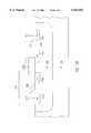
- FIG. 1shows one such latch described in U.S. Pat. No. 4,546,455 issued Oct. 8, 1985 to Iwahashi et al.
- Fuse F1is connected between the power supply terminal VDD and the latch output terminal OUT.
- An NMOS transistor 110is connected between the terminal OUT and the ground terminal.
- Three serially connected inverters 120.1, 120.2, 120.3are provided between the output terminal OUT and the gate of transistor 110.
- fuse F1If fuse F1 is intact, the terminal OUT is pulled to VDD.
- the inverters 120keep transistor 110 off. If fuse F1 is blown, the terminal OUT is at the ground voltage. The inverters turn transistor 110 on to keep the terminal OUT at ground.
- Bypass capacitor 130is connected between the input of inverter 120.3 and the ground terminal to insure correct initialization of the latch on power-up. More particularly, when the power is off, transistor 110 is non-conductive. Therefore, terminal OUT is floating. According to U.S. Pat. No. 4,546,455, the terminal OUT may "tend to have its potential raised to a logic level ⁇ 1 ⁇ ". In addition, the terminal OUT potential may become "unstable due to the capacitive coupling" in the integrated circuit. Consequently, during operation, transistor 110 could be off even if the fuse F1 were blown. As a result, the terminal OUT would provide an erroneous voltage.
- Capacitor 130is intended to avoid such malfunction. During power up, capacitor 130 keeps the input of inverter 120.3 low sufficiently long to allow the inverter to turn on transistor 110 and discharge the terminal OUT to ground if the fuse is blown. Then the ground voltage on terminal OUT propagates through the three inverters to keep transistor 110 on.
- Some embodiments of the present inventionprovide simple and reliable programmable latches. Some programmable latches are reliable because they do not depend on delays such as delays provided by capacitor 130. Dependence on delays is undesirable because delay-dependent circuits may not operate properly if VDD rises slowly. Some latches are simple because they omit capacitor 130 and include only one CMOS inverter.
- a diodethat keeps a voltage on a latch output terminal within a predetermined range of values before power is supplied to the latch.
- the diode's anodeis connected to terminal OUT, and the cathode is connected to an external power supply pin EVCC or to a reference voltage terminal.
- the EVCC pin or the reference voltage terminalis at ground, and therefore the voltage on the terminal OUT is not higher than one diode threshold voltage relative to ground (0.65V in some embodiments.)
- the maximum voltage of 0.65V on terminal OUTallows the latch to be powered up correctly even if fuse F1 is blown.
- the diode's cathodeis connected to a reference voltage which is used also in other parts of the integrated circuit.
- the reference voltageis generated by a reference voltage generator which includes one or more pull-down resistors connected to the reference voltage terminal and to the ground terminal. When the power is off, these resistors discharge the reference voltage terminal to ground. Hence, the OUT voltage is not higher than one diode threshold relative to ground when the power is off.
- Prior art latch of FIG. 1has an advantage that a latch initialization does not require a latch initialization signal from outside the latch.
- the state of the latchis completely determined by the state of fuse F1 and the voltages on the VDD and ground terminals. This advantage is preserved in some embodiments of the present invention. This advantageously distinguishes such embodiments of the invention from the latch described in U.S. Pat. No. 5,566,107 issued Oct. 15, 1996 to Gilliam in describing a circuit that needs an external "activate" signal for initialization.
- Some embodimentsdo not include a capacitor to generate a delay.
- only one inverter having a pull-up device and one pull-down deviceis provided between the output terminal OUT and the gate of transistor 110.
- Some embodiments with only one CMOS inverter and no capacitoroperate successfully even without a diode because in such embodiments the voltage on the terminal OUT is at the ground level before the power is turned on. The voltage could drift away from the ground level during fuse programming if, for example, the fuse is programmed electrically. (Of note, some embodiments use laser programmable fuses rather than electrically programmable fuses.) However, even if the voltage on terminal OUT becomes high when the fuse is being programmed, the power is turned off after programming, and the voltage on the terminal OUT is allowed to return to ground before the power is turned on again.
- the latchoperates properly due to the selection of the trip voltage of the inverter and/or the threshold voltage of transistor 110.
- FIG. 1is a circuit diagram of a prior art programmable latch.
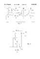
- FIG. 2Ais a circuit diagram of a programmable latch according to the present invention.
- FIG. 2Billustrates a semiconductor cross section of the latch of FIG. 2A.
- FIG. 3is a circuit diagram illustrating a reference voltage generator that powers the latch of FIG. 2A.
- FIGS. 4 and 5are circuit diagrams of alternative reference voltage generators for the latch of FIG. 2A.
- FIGS. 6-8are circuit diagrams of programmable latches according to the present invention.
- FIG. 2Aillustrates a programmable latch 210 according to the present invention.
- Terminal 211 of fuse F1is connected to a terminal 212 providing a constant non-ground voltage VINT.
- Voltage VINTis an internal power supply voltage generated by VINT generator 213 from an external power supply voltage EVCC received on an external pin 214 of the integrated circuit containing the latch 210. Voltage VINT also powers other parts of the integrated circuit. Voltage VINT is a positive voltage.
- Terminal 215 of fuse F1is connected to terminal OUT.
- the terminal OUTis connected to the drain of NMOS transistor 110 whose source is connected to a ground terminal.
- Terminal OUTis connected to the input of CMOS inverter 120 formed by PMOS pull-up transistor 220 and NMOS pull-down transistor 230.
- the inverter inputis connected to the gates of transistors 220, 230.
- the source of transistor 220is connected to VINT terminal 212.
- the source of transistor 230is connected to the ground terminal.
- the drains of the two transistorsare connected to complimentary output terminal OUT- of latch 210.
- Terminal OUT-is connected to the gate of transistor 110.
- Diode 234has its anode terminal 238 connected to terminal OUT and its cathode terminal 240 connected to the VINT terminal 212.
- the VINT terminalWhen the power is off, the VINT terminal is at ground. (VINT terminal is connected to ground by a resistor network in generator 213, as described below in connection with FIG. 3.) Therefore, the voltage on the terminal OUT is not higher than one threshold voltage of diode 234.
- diode 234is a silicon PN junction diode, the voltage on terminal OUT is not higher than 0.65V. This value is below the trip voltage of inverter 120 and even below the threshold voltage of NMOS transistor 230 (the threshold voltage of transistor 230 is 1.2V in some embodiments). Therefore, if fuse F1 is blown, transistor 230 remains off when the power is turned on. As soon as transistor 220 charges the gate of transistor 110 to the threshold voltage of transistor 110, transistor 110 connects the terminal OUT to ground.
- FIG. 2Billustrates a cross section of a portion of the integrated circuit incorporating the latch 210 in some embodiments.
- the source 220S and the drain 220D of transistor 220are P+ semiconductor regions in N well 242 in P substrate 244.
- Gate 220G of transistor 220is separated from N well 242 by silicon dioxide (not shown).
- the N wellis connected to the VINT terminal via an ohmic contact in the N+ region 246 formed in the N well.
- the diode cathode 238is a P+ region formed in the N well.
- the diodeis formed by the PN junction between the region 238 and the surrounding region 240 of N well 242.
- the state of the latch(the voltage on the terminal OUT) during the latch operation is completely determined by the state of fuse F1 and by the voltages on the terminal 212 and the ground terminal.
- FIG. 3shows one embodiment of VINT generator 213.
- the output terminal 212 of the VINT generatoris connected to ground by a resistor network which includes: (1) resistors R1, R2, R3 connected in parallel between terminal 212 and a node FD; and (2) resistor R4 interconnecting the node FD and the ground terminal.
- the pull-up path between the terminal 212 and the external voltage supply EVCCis through PMOS transistor 310.
- the gate of transistor 310is connected to the output of a differential amplifier formed by PMOS transistors 314, 318 and NMOS transistors 322, 326, 330 and 334.
- the sources of transistors 314, 318are connected to the EVCC pin.
- the gatesare connected to each other and to the drain of transistor 314.
- the drain of transistor 318is the amplifier output connected to the gate of transistor 310.
- the drain of transistor 318is also connected to the drain of transistor 326.
- the drain of transistor 314is connected to the drain of transistor 322.
- the gate of transistor 322is connected to the node FD.
- the gate of transistor 326receives a reference voltage VREF generated by some reference voltage generator (not shown) as known in the art.
- the sources of transistors 322, 326are connected to the drain of transistor 330.
- the source of transistor 330is connected to the drain of transistor 334.
- the source of transistor 334is connected to ground.
- the gate of transistor 334receives a reference voltage VCMN generated by a reference voltage generator (not shown).
- the gate of transistor 334is also connected to ground through MOS capacitor 340.
- a MOS capacitoris a capacitor formed by a MOS transistor whose source and drain are shorted together.
- the gate of transistor 330receives an enable signal EN.
- the signal ENis also delivered to the gate of PMOS transistor 344 whose drain is connected to the gate of transistor 310 and whose source is connected EVCC.
- ENWhen EN is low (ground), the VINT terminal 212 is at ground.
- ENis at EVCC, the terminal 212 provides a voltage between ground and EVCC.
- Terminal 212is connected to node FD by MOS capacitor 350.
- Node FDis connected to the drain of NMOS transistor 354.
- the source node 358 of transistor 354is connected to the drain of transistor 362 whose source is connected to ground.
- Node 358is connected to terminal 212 through MOS capacitor 366.
- the gate of transistor 362is connected to the output of NAND gate 370.
- the output of gate 370is also connected to the input of inverter 374 whose output is connected to the gate of transistor 354.
- One input of two-input gate 370receives the enable signal EN.
- the enable signal ENis delivered to the other output of gate 370 through three serially connected inverters 374, 378, 382.
- voltage VINT on terminal 212is an internal power supply voltage that powers also other parts of the integrated circuit containing the latch 210.
- the integrated circuitis a synchronous dynamic random access memory (SDRAM).
- SDRAMsynchronous dynamic random access memory
- the voltage VINTpowers the memory address decoders, command decoding circuitry, burst counting circuitry, and input buffers such as clock enable buffer 386.
- Buffer 386receives a clock enable signal CKE from an external pin and generates an internal clock enable ICKE at ground and VINT voltage levels.
- the synchronous DRAMincludes several generators 213. Each generator is enabled by its own signal EN. Thus, selective generators 213 can be disabled to reduce power consumption (in stand-by mode, for example). However, at least one generator 213 is enabled throughout the circuit operation in order to power circuits that are never disabled, for example, the buffer 386. Hence, the VINT voltage is a constant value throughout the operation of the integrated circuit.
- the outputs 212 of some or all of the generators 213are shorted together. However, some generators 213 are sometimes disabled (in stand-by mode for example) when the current drawn from the common terminal 212 of generators 213 is reduced.
- Addendum Aprovides transistor sizes and resistor values and some other particulars for one embodiment of a VINT generator 213.
- FIGS. 4 and 5show other embodiments of a VINT generator 213.
- VINT generator 213is a voltage divider formed by resistors 410, 420 connected in series between EVCC pin 214 and the ground pin of the integrated circuit.
- resistor 420is replaced by an NMOS transistor (a long channel transistor in some embodiments) whose body region is connected to the ground terminal.
- the gate of transistor 420receives a reference voltage VREF.
- This voltageis generated by a voltage divider consisting of resistors 510, 520 connected in series between EVCC and ground.
- the VREF terminalis at ground, and transistor 420 is off.
- the drain/body diode of transistor 420does not allow the voltage on terminal 212 to rise above one diode threshold relative to ground.
- Latch 210 of FIG. 6is identical to the latch of FIG. 2A except that in FIG. 6 the diode cathode 240 is connected to EVCC pin 214.
- Some embodimentsinclude two diodes, with one diode connected as in FIG. 6 and the other diode connected as in FIG. 2A. Some embodiments include diodes connected in series or in parallel between the terminal OUT and the terminal 212 or 214.
- the terminals 211 and 240are both connected to the EVCC terminal 214.
- Inverter 120is powered by EVCC.
- the EVCC terminalis at ground because the integrated circuit includes a voltage divider, such as the voltage divider 213 of FIG. 4, to generate an intermediate voltage.
- diode 234is omitted. Nevertheless, if fuse F1 is non-conductive, the terminal OUT is at ground before power-up. This is true even if the fuse was programmed electrically and some charge accumulated on terminal OUT during programming. Indeed, after the fuse is programmed (that is, made non-conductive), the power is kept off for a while before the latch is used. For example, if the latch is part of a semiconductor memory, the memory fuses are typically programmed when the memory is tested. Then the power is turned off, and the memory is taken out of the testing equipment and shipped to a customer. By the time the customer supplies power to the memory, any charge which may have accumulated on terminal OUT when the fuse was being programmed has been dissipated. Therefore, the terminal OUT is at ground.
- transistor 110turns on and keeps the node OUT at the ground voltage.
- the terminal OUTis quickly returned to ground. If the power is turned off and then turned on again, the terminal OUT is at zero volts before the power is turned on. Therefore, reliable operation is provided.
- the inverter 120 trip voltagemeasured when EVCC has reached its final value, is made high to ensure that the trip voltage will be higher than any voltage on terminal OUT.
- the trip voltagecan be made large by making transistor 220 large relative to transistor 230, or by increasing the threshold voltage of transistor 230, or by other methods known or to be discovered.
- the threshold voltage of transistor 110is made low (lower than the threshold voltages of other NMOS transistors, including transistor 230, in the same integrated circuit), so that even if the terminal OUT is slightly above the inverter trip voltage when the fuse is blown, the inverter will charge the complementary terminal OUT- to a sufficiently high voltage to pull the terminal OUT down. As the terminal OUT is being pulled down, the voltage on terminal OUT- increases, the current through transistor 110 also increases, and eventually the terminal OUT is pulled to ground by the transistor 110.
- EVCC3.3V
- the threshold voltage of transistor 230is 1.2V
- the threshold voltage of transistor 220is -0.8V
- the threshold voltage of transistor 110is 0.5V.
- the trip voltage of inverter 120is 1.6V at the final EVCC value of 3.3V.
- FIG. 7illustrates another embodiment of latch 210.
- Fuse F1 and diode 234are connected to terminals VINT and OUT, and NMOS transistor 110 is connected to the terminal OUT and to the ground terminal, as in FIG. 2A.
- three inverters 120.1, 120.2, 120.3are provided between the terminal OUT and the gate of transistor 110.
- inverter 120.1the gates of PMOS transistor 220.1 and NMOS transistor 230.1 are connected to the terminal OUT.
- the source of transistor 220.1is connected to VINT.
- the source of transistor 230.1is connected to ground.
- the drains of transistors 220.1, 230.1are connected to the gates of PMOS transistor 220.2 and NMOS transistor 230.2 of inverter 120.2.
- the drains of transistor 220.2, 230.2are connected to the gates of PMOS transistor 220.3 and NMOS transistor 230.3 of inverter 120.3.
- the sources of transistors 220.2, 220.3are connected to the VINT terminal 212.
- the sources of transistors 230.2, 230.3are connected to ground.
- the drains of transistors 220.3, 230.3are connected to the gate of transistor 110.
- the voltage VINTis generated by some voltage generator such as the generator 213 of FIG. 3.
- diode 234is omitted, or its cathode is connected to EVCC pin 214.
- inverter 120.1(the terminal connected to the drains of transistors 220.1, 230.1) is the complimentary output OUT- of latch 210.
- terminal OUTis at VINT, and the three inverters keep transistor 110 off. If the fuse is blown, then terminal OUT is at ground, or is at most one diode threshold above ground, for essentially the same reasons as those explained above in connection with FIG. 2A. Therefore, when the power is supplied, transistor 110 is turned on.
- the trip voltage of inverter 120.1is made high to ensure that when the fuse is blown, the trip voltage will be higher than any possible voltage on the terminal OUT.
- the threshold voltage of transistor 110is made low (lower than threshold voltages of other NMOS transistors in the same integrated circuit) to facilitate discharge of terminal OUT, similarly to the FIG. 2A embodiment.
- Some embodimentsinclude five inverters, or some other number of inverters, connected in series between the terminal OUT and the gate of transistor 110.
- Latch 210 of FIG. 8is similar to the latch of FIG. 2A, but the supply voltage EVCC and the voltage VINT are negative.
- Transistors 110 and 230are PMOS transistors.
- Transistor 220is an NMOS transistor.
- Diode 234has its anode connected to VINT terminal 212 and its cathode connected to terminal OUT.
- Some embodiments of the latch of FIG. 7 or of latches with five or more invertersalso use negative supply voltages.
- Some embodimentsuse a non-ground reference voltage instead of the ground.
- fuse F1is a laser programmable fuse made of polysilicon, metal (for example, aluminum), or some other conductive material.
- the fuse F1is an electrically programmable fuse, for example, a polysilicon fuse which can be blown by current supplied through another transistor (not shown).
- fuse F1is replaced by some other programmable element, for example, an antifuse, an EPROM, EEPROM, or UPROM cell (see B. Prince, "Semiconductor Memories” (1991), pages 762-764 incorporate herein by reference), or some other non-volatile programmable element known or to be discovered.
- the inverters 120 of FIGS. 2A, 7, 8are non-CMOS inverters.
- the pull-up transistors 220are replaced by suitable resistors or depletion mode transistors.
- Programmable latches 210are suitable for use in a wide variety of memory and non-memory circuits. Some latch embodiments are used in dynamic random access memories. Some latch embodiments are used in spare row and column decoders to select spare rows or columns. Such use of programmable latches is described in U.S. Pat. No. 4,546,455 issued Oct. 8, 1985 to Iwahashi et al. and incorporated herein by reference. In some embodiments, programmable latches 210 are used to adjust delay times or select a clock signal, as described in U.S. Pat. No. 5,440,246 issued Aug. 8, 1995 to Murray et al. and incorporated herein by reference.
- the latches 210are used to salvage defective memories as described in U.S. patent application Ser. No. 08/840,337 filed Apr. 28, 1997 by Li-Chun Li, now U.S. Pat. No. 5,889,414 issued on Mar. 30, 1999, incorporated herein by reference.
- transistor 110is replaced by a variable-impedance electrical path which includes a number of transistors connected in series or in parallel between the terminal OUT and the ground terminal. One or more of the transistors have their gates connected to the output of inverter 120 or 120.3. In some embodiments, other circuit elements (such as resistors, perhaps variable-impedance resistors) are included between the terminal OUT and the ground or VINT terminals. In some embodiments, diode 234 is a Schottky diode. Other embodiments and variations are within the scope of the invention, as defined by the appended claims.
- the table belowspecifies transistor channel width/length dimensions (in micrometers) and resistor values for one embodiment of a VINT generator 213 of FIG. 3.
- the NAND gate 370 and all the invertersare CMOS circuits.
- Each resistor R1, R2, R3, R4is an N-type diffusion region in a P-type monocrystalline silicon substrate region biased at ground.
Landscapes
- Semiconductor Integrated Circuits (AREA)
- Design And Manufacture Of Integrated Circuits (AREA)
Abstract
Description
______________________________________ Device Specification ______________________________________ Resistor R1 5.6 KΩ Resistor R2 90 KΩ Resistor R3 90 KΩ Resistor R4 6KΩ Transistor 310 1000/1Transistor 314 50/0.6Transistor 318 100/0.6Transistor 322 50/0.6Transistor 326 100/0.6Transistors 330 100/1 Transistor 334 100/1Transistor 340 2/15Transistor 344 2/2Transistor 350 2/100Transistor 354 20/1Transistor 362 4/1Transistor 366 2/70NAND gate 370 10/1 for each transistor Inverter 374 P = 6/1 (PMOS transistor width length), N = 6/1 (NMOS transistor width/length)374, 378, 382 P = 5/1, N = 2/2 ______________________________________ Inverters
Claims (21)
Priority Applications (4)
| Application Number | Priority Date | Filing Date | Title |
|---|---|---|---|
| US09/178,445US6163492A (en) | 1998-10-23 | 1998-10-23 | Programmable latches that include non-volatile programmable elements |
| US09/516,336US6266290B1 (en) | 1998-10-23 | 2000-03-01 | Programmable latches that include non-volatile programmable elements |
| US09/669,780US6222776B1 (en) | 1998-10-23 | 2000-09-25 | Programmable latches that include non-volatile programmable elements |
| US09/669,992US6240034B1 (en) | 1998-10-23 | 2000-09-25 | Programmable latches that include non-volatile programmable elements |
Applications Claiming Priority (1)
| Application Number | Priority Date | Filing Date | Title |
|---|---|---|---|
| US09/178,445US6163492A (en) | 1998-10-23 | 1998-10-23 | Programmable latches that include non-volatile programmable elements |
Related Child Applications (1)
| Application Number | Title | Priority Date | Filing Date |
|---|---|---|---|
| US09/516,336DivisionUS6266290B1 (en) | 1998-10-23 | 2000-03-01 | Programmable latches that include non-volatile programmable elements |
Publications (1)
| Publication Number | Publication Date |
|---|---|
| US6163492Atrue US6163492A (en) | 2000-12-19 |
Family
ID=22652570
Family Applications (4)
| Application Number | Title | Priority Date | Filing Date |
|---|---|---|---|
| US09/178,445Expired - LifetimeUS6163492A (en) | 1998-10-23 | 1998-10-23 | Programmable latches that include non-volatile programmable elements |
| US09/516,336Expired - LifetimeUS6266290B1 (en) | 1998-10-23 | 2000-03-01 | Programmable latches that include non-volatile programmable elements |
| US09/669,780Expired - LifetimeUS6222776B1 (en) | 1998-10-23 | 2000-09-25 | Programmable latches that include non-volatile programmable elements |
| US09/669,992Expired - LifetimeUS6240034B1 (en) | 1998-10-23 | 2000-09-25 | Programmable latches that include non-volatile programmable elements |
Family Applications After (3)
| Application Number | Title | Priority Date | Filing Date |
|---|---|---|---|
| US09/516,336Expired - LifetimeUS6266290B1 (en) | 1998-10-23 | 2000-03-01 | Programmable latches that include non-volatile programmable elements |
| US09/669,780Expired - LifetimeUS6222776B1 (en) | 1998-10-23 | 2000-09-25 | Programmable latches that include non-volatile programmable elements |
| US09/669,992Expired - LifetimeUS6240034B1 (en) | 1998-10-23 | 2000-09-25 | Programmable latches that include non-volatile programmable elements |
Country Status (1)
| Country | Link |
|---|---|
| US (4) | US6163492A (en) |
Cited By (2)
| Publication number | Priority date | Publication date | Assignee | Title |
|---|---|---|---|---|
| US6240034B1 (en)* | 1998-10-23 | 2001-05-29 | Mosel Vitelic, Inc. | Programmable latches that include non-volatile programmable elements |
| US20180047670A1 (en)* | 2016-08-09 | 2018-02-15 | Skyworks Solutions, Inc. | Programmable fuse with single fuse pad and control methods thereof |
Families Citing this family (9)
| Publication number | Priority date | Publication date | Assignee | Title |
|---|---|---|---|---|
| DE19922360C2 (en)* | 1999-05-14 | 2001-05-10 | Siemens Ag | Circuit arrangement for programming an electrically programmable element |
| US6452770B1 (en)* | 2000-05-31 | 2002-09-17 | Lucent Technologies Inc. | Power buss inhibit through data input/output lines |
| US7312109B2 (en)* | 2002-07-08 | 2007-12-25 | Viciciv, Inc. | Methods for fabricating fuse programmable three dimensional integrated circuits |
| EP1533128A3 (en)* | 2003-02-05 | 2005-12-07 | International United Technology Co., Ltd. | Ink jet printhead identification circuit and method |
| KR100554840B1 (en)* | 2003-11-13 | 2006-03-03 | 주식회사 하이닉스반도체 | Power-up signal generator |
| US7098491B2 (en)* | 2003-12-30 | 2006-08-29 | Taiwan Semiconductor Manufacturing Company, Ltd. | Protection circuit located under fuse window |
| US7236418B2 (en)* | 2004-06-25 | 2007-06-26 | Qualcomm Incorporated | Reduced area, reduced programming voltage CMOS eFUSE-based scannable non-volatile memory bitcell |
| CN100541669C (en)* | 2006-03-29 | 2009-09-16 | 富晶半导体股份有限公司 | Burning checking method and circuit thereof |
| JP5149576B2 (en)* | 2007-09-21 | 2013-02-20 | パナソニック株式会社 | Semiconductor device |
Citations (36)
| Publication number | Priority date | Publication date | Assignee | Title |
|---|---|---|---|---|
| DE288689C (en)* | ||||
| US4387503A (en)* | 1981-08-13 | 1983-06-14 | Mostek Corporation | Method for programming circuit elements in integrated circuits |
| US4404635A (en)* | 1981-03-27 | 1983-09-13 | International Business Machines Corporation | Programmable integrated circuit and method of testing the circuit before it is programmed |
| US4532607A (en)* | 1981-07-22 | 1985-07-30 | Tokyo Shibaura Denki Kabushiki Kaisha | Programmable circuit including a latch to store a fuse's state |
| US4532402A (en)* | 1983-09-02 | 1985-07-30 | Xrl, Inc. | Method and apparatus for positioning a focused beam on an integrated circuit |
| US4546455A (en)* | 1981-12-17 | 1985-10-08 | Tokyo Shibaura Denki Kabushiki Kaisha | Semiconductor device |
| US4571704A (en)* | 1984-02-17 | 1986-02-18 | Hughes Aircraft Company | Nonvolatile latch |
| US4614881A (en)* | 1983-02-04 | 1986-09-30 | Fujitsu Limited | Integrated semiconductor circuit device for generating a switching control signal using a flip-flop circuit including CMOS FET's and flip-flop setting means |
| US4617651A (en)* | 1984-02-22 | 1986-10-14 | Seeq Technology, Inc. | Redundancy circuit for use in a semiconductor memory array |
| US4725979A (en)* | 1986-12-05 | 1988-02-16 | Monolithic Memories, Inc. | Emitter coupled logic circuit having fuse programmable latch/register bypass |
| US4771285A (en)* | 1985-11-05 | 1988-09-13 | Advanced Micro Devices, Inc. | Programmable logic cell with flexible clocking and flexible feedback |
| US4779229A (en)* | 1986-07-02 | 1988-10-18 | Advanced Micro Devices, Inc. | Prom with programmable output structures |
| US4837520A (en)* | 1985-03-29 | 1989-06-06 | Honeywell Inc. | Fuse status detection circuit |
| US4852044A (en)* | 1985-03-04 | 1989-07-25 | Lattice Semiconductor Corporation | Programmable data security circuit for programmable logic device |
| US4943804A (en)* | 1988-03-02 | 1990-07-24 | Dallas Semiconductor Corporation | Electronic key locking circuitry |
| US5066998A (en)* | 1989-06-30 | 1991-11-19 | At&T Bell Laboratories | Severable conductive path in an integrated-circuit device |
| US5086331A (en)* | 1988-04-05 | 1992-02-04 | U.S. Philips Corp. | Integrated circuit comprising a programmable cell |
| US5134585A (en)* | 1989-06-05 | 1992-07-28 | Mitsubishi Denki Kabushiki Kaisha | Circuit for repairing defective bit in semiconductor memory device and repairing method |
| US5185291A (en)* | 1989-06-30 | 1993-02-09 | At&T Bell Laboratories | Method of making severable conductive path in an integrated-circuit device |
| US5285953A (en)* | 1993-04-26 | 1994-02-15 | Smith Robert B | Beverage cup holder |
| US5440246A (en)* | 1994-03-22 | 1995-08-08 | Mosel Vitelic, Incorporated | Programmable circuit with fusible latch |
| US5455937A (en)* | 1991-11-12 | 1995-10-03 | Microchip Technology, Inc. | Microcontroller with fuse-emulating latches |
| US5459684A (en)* | 1993-02-19 | 1995-10-17 | Hitachi, Ltd. | Dynamic RAM, dynamic RAM plate voltage setting method, and information processing system |
| US5497355A (en)* | 1994-06-03 | 1996-03-05 | Intel Corporation | Synchronous address latching for memory arrays |
| US5506638A (en)* | 1993-09-03 | 1996-04-09 | Donner, Inc. | Spectacles with weight bearing cheek rest |
| US5526320A (en)* | 1994-12-23 | 1996-06-11 | Micron Technology Inc. | Burst EDO memory device |
| US5544124A (en)* | 1995-03-13 | 1996-08-06 | Micron Technology, Inc. | Optimization circuitry and control for a synchronous memory device with programmable latency period |
| US5566107A (en)* | 1995-05-05 | 1996-10-15 | Micron Technology, Inc. | Programmable circuit for enabling an associated circuit |
| US5640364A (en)* | 1994-12-23 | 1997-06-17 | Micron Technology, Inc. | Self-enabling pulse trapping circuit |
| US5696455A (en)* | 1994-09-28 | 1997-12-09 | Altera Corporation | Reconfigurable programmable logic device |
| US5710741A (en)* | 1994-03-11 | 1998-01-20 | Micron Technology, Inc. | Power up intialization circuit responding to an input signal |
| US5793688A (en)* | 1995-06-30 | 1998-08-11 | Micron Technology, Inc. | Method for multiple latency synchronous dynamic random access memory |
| US5812489A (en)* | 1996-03-29 | 1998-09-22 | Nec Corporation | Single-chip synchronous dynamic random access memory (DRAM) system |
| US5870342A (en)* | 1997-06-25 | 1999-02-09 | Mitsubishi Denki Kabushiki Kaisha | Semiconductor memory device surely reset upon power on |
| US5892712A (en)* | 1996-05-01 | 1999-04-06 | Nvx Corporation | Semiconductor non-volatile latch device including embedded non-volatile elements |
| US5898621A (en)* | 1994-05-19 | 1999-04-27 | Hitachi, Ltd. | Batch erasable single chip nonvolatile memory device and erasing method therefor |
Family Cites Families (7)
| Publication number | Priority date | Publication date | Assignee | Title |
|---|---|---|---|---|
| US4906870A (en)* | 1988-10-31 | 1990-03-06 | Atmel Corporation | Low power logic array device |
| JP2888034B2 (en) | 1991-06-27 | 1999-05-10 | 日本電気株式会社 | Semiconductor memory device |
| US5740106A (en)* | 1995-06-29 | 1998-04-14 | Cypress Semiconductor Corp. | Apparatus and method for nonvolatile configuration circuit |
| US5952833A (en)* | 1997-03-07 | 1999-09-14 | Micron Technology, Inc. | Programmable voltage divider and method for testing the impedance of a programmable element |
| US5889414A (en)* | 1997-04-28 | 1999-03-30 | Mosel Vitelic Corporation | Programmable circuits |
| US6163492A (en)* | 1998-10-23 | 2000-12-19 | Mosel Vitelic, Inc. | Programmable latches that include non-volatile programmable elements |
| US6084803A (en)* | 1998-10-23 | 2000-07-04 | Mosel Vitelic, Inc. | Initialization of non-volatile programmable latches in circuits in which an initialization operation is performed |
- 1998
- 1998-10-23USUS09/178,445patent/US6163492A/ennot_activeExpired - Lifetime
- 2000
- 2000-03-01USUS09/516,336patent/US6266290B1/ennot_activeExpired - Lifetime
- 2000-09-25USUS09/669,780patent/US6222776B1/ennot_activeExpired - Lifetime
- 2000-09-25USUS09/669,992patent/US6240034B1/ennot_activeExpired - Lifetime
Patent Citations (36)
| Publication number | Priority date | Publication date | Assignee | Title |
|---|---|---|---|---|
| DE288689C (en)* | ||||
| US4404635A (en)* | 1981-03-27 | 1983-09-13 | International Business Machines Corporation | Programmable integrated circuit and method of testing the circuit before it is programmed |
| US4532607A (en)* | 1981-07-22 | 1985-07-30 | Tokyo Shibaura Denki Kabushiki Kaisha | Programmable circuit including a latch to store a fuse's state |
| US4387503A (en)* | 1981-08-13 | 1983-06-14 | Mostek Corporation | Method for programming circuit elements in integrated circuits |
| US4546455A (en)* | 1981-12-17 | 1985-10-08 | Tokyo Shibaura Denki Kabushiki Kaisha | Semiconductor device |
| US4614881A (en)* | 1983-02-04 | 1986-09-30 | Fujitsu Limited | Integrated semiconductor circuit device for generating a switching control signal using a flip-flop circuit including CMOS FET's and flip-flop setting means |
| US4532402A (en)* | 1983-09-02 | 1985-07-30 | Xrl, Inc. | Method and apparatus for positioning a focused beam on an integrated circuit |
| US4571704A (en)* | 1984-02-17 | 1986-02-18 | Hughes Aircraft Company | Nonvolatile latch |
| US4617651A (en)* | 1984-02-22 | 1986-10-14 | Seeq Technology, Inc. | Redundancy circuit for use in a semiconductor memory array |
| US4852044A (en)* | 1985-03-04 | 1989-07-25 | Lattice Semiconductor Corporation | Programmable data security circuit for programmable logic device |
| US4837520A (en)* | 1985-03-29 | 1989-06-06 | Honeywell Inc. | Fuse status detection circuit |
| US4771285A (en)* | 1985-11-05 | 1988-09-13 | Advanced Micro Devices, Inc. | Programmable logic cell with flexible clocking and flexible feedback |
| US4779229A (en)* | 1986-07-02 | 1988-10-18 | Advanced Micro Devices, Inc. | Prom with programmable output structures |
| US4725979A (en)* | 1986-12-05 | 1988-02-16 | Monolithic Memories, Inc. | Emitter coupled logic circuit having fuse programmable latch/register bypass |
| US4943804A (en)* | 1988-03-02 | 1990-07-24 | Dallas Semiconductor Corporation | Electronic key locking circuitry |
| US5086331A (en)* | 1988-04-05 | 1992-02-04 | U.S. Philips Corp. | Integrated circuit comprising a programmable cell |
| US5134585A (en)* | 1989-06-05 | 1992-07-28 | Mitsubishi Denki Kabushiki Kaisha | Circuit for repairing defective bit in semiconductor memory device and repairing method |
| US5185291A (en)* | 1989-06-30 | 1993-02-09 | At&T Bell Laboratories | Method of making severable conductive path in an integrated-circuit device |
| US5066998A (en)* | 1989-06-30 | 1991-11-19 | At&T Bell Laboratories | Severable conductive path in an integrated-circuit device |
| US5455937A (en)* | 1991-11-12 | 1995-10-03 | Microchip Technology, Inc. | Microcontroller with fuse-emulating latches |
| US5459684A (en)* | 1993-02-19 | 1995-10-17 | Hitachi, Ltd. | Dynamic RAM, dynamic RAM plate voltage setting method, and information processing system |
| US5285953A (en)* | 1993-04-26 | 1994-02-15 | Smith Robert B | Beverage cup holder |
| US5506638A (en)* | 1993-09-03 | 1996-04-09 | Donner, Inc. | Spectacles with weight bearing cheek rest |
| US5710741A (en)* | 1994-03-11 | 1998-01-20 | Micron Technology, Inc. | Power up intialization circuit responding to an input signal |
| US5440246A (en)* | 1994-03-22 | 1995-08-08 | Mosel Vitelic, Incorporated | Programmable circuit with fusible latch |
| US5898621A (en)* | 1994-05-19 | 1999-04-27 | Hitachi, Ltd. | Batch erasable single chip nonvolatile memory device and erasing method therefor |
| US5497355A (en)* | 1994-06-03 | 1996-03-05 | Intel Corporation | Synchronous address latching for memory arrays |
| US5696455A (en)* | 1994-09-28 | 1997-12-09 | Altera Corporation | Reconfigurable programmable logic device |
| US5526320A (en)* | 1994-12-23 | 1996-06-11 | Micron Technology Inc. | Burst EDO memory device |
| US5640364A (en)* | 1994-12-23 | 1997-06-17 | Micron Technology, Inc. | Self-enabling pulse trapping circuit |
| US5544124A (en)* | 1995-03-13 | 1996-08-06 | Micron Technology, Inc. | Optimization circuitry and control for a synchronous memory device with programmable latency period |
| US5566107A (en)* | 1995-05-05 | 1996-10-15 | Micron Technology, Inc. | Programmable circuit for enabling an associated circuit |
| US5793688A (en)* | 1995-06-30 | 1998-08-11 | Micron Technology, Inc. | Method for multiple latency synchronous dynamic random access memory |
| US5812489A (en)* | 1996-03-29 | 1998-09-22 | Nec Corporation | Single-chip synchronous dynamic random access memory (DRAM) system |
| US5892712A (en)* | 1996-05-01 | 1999-04-06 | Nvx Corporation | Semiconductor non-volatile latch device including embedded non-volatile elements |
| US5870342A (en)* | 1997-06-25 | 1999-02-09 | Mitsubishi Denki Kabushiki Kaisha | Semiconductor memory device surely reset upon power on |
Non-Patent Citations (6)
| Title |
|---|
| "Synchronous Graphics RAM" Micron Technology, Inc. of Bosie Idaho, 1998, pp. 1-45. |
| B. Prince, "High Performance Memories" New Architecture DRAMs and SRAMs Evolution and Function,1996 , pp. 135-227. |
| B. Prince, "Semiconductor Memories" A Handbook of Design, Manufacture and Application, Second Edition, (1991), pp. 762-764. |
| B. Prince, High Performance Memories New Architecture DRAMs and SRAMs Evolution and Function,1996 , pp. 135 227.* |
| B. Prince, Semiconductor Memories A Handbook of Design, Manufacture and Application, Second Edition, (1991), pp. 762 764.* |
| Synchronous Graphics RAM Micron Technology, Inc. of Bosie Idaho, 1998, pp. 1 45.* |
Cited By (3)
| Publication number | Priority date | Publication date | Assignee | Title |
|---|---|---|---|---|
| US6240034B1 (en)* | 1998-10-23 | 2001-05-29 | Mosel Vitelic, Inc. | Programmable latches that include non-volatile programmable elements |
| US20180047670A1 (en)* | 2016-08-09 | 2018-02-15 | Skyworks Solutions, Inc. | Programmable fuse with single fuse pad and control methods thereof |
| US11978701B2 (en)* | 2016-08-09 | 2024-05-07 | Skyworks Solutions, Inc. | Programmable fuse with single fuse pad and control methods thereof |
Also Published As
| Publication number | Publication date |
|---|---|
| US6240034B1 (en) | 2001-05-29 |
| US6222776B1 (en) | 2001-04-24 |
| US6266290B1 (en) | 2001-07-24 |
Similar Documents
| Publication | Publication Date | Title |
|---|---|---|
| US5448199A (en) | Internal supply voltage generation circuit | |
| US6400632B1 (en) | Semiconductor device including a fuse circuit in which the electric current is cut off after blowing so as to prevent voltage fall | |
| US5097146A (en) | Circuit for detecting high voltage level in mos technology | |
| WO2007040851A1 (en) | Antifuse circuit with current regulator for controlling programming current | |
| US6163492A (en) | Programmable latches that include non-volatile programmable elements | |
| US6225852B1 (en) | Use of biased high threshold voltage transistor to eliminate standby current in low voltage integrated circuits | |
| US6229365B1 (en) | Semiconductor integrated circuit device operating stably at a plurality of power supply voltage levels | |
| US6724601B2 (en) | ESD protection circuit | |
| US6778000B2 (en) | Integrated circuit devices that provide constant time delays irrespective of temperature variation | |
| US11342906B2 (en) | Delay circuits, and related semiconductor devices and methods | |
| US4791614A (en) | Semiconductor memory device having erroneous write operation preventing function | |
| US6128230A (en) | Semiconductor memory with PN junction potential reduction in a writing mode | |
| US6859067B2 (en) | Semiconductor apparatus | |
| US8258856B2 (en) | Antifuse circuit having protection circuit | |
| US7099223B2 (en) | Semiconductor memory device | |
| US7046054B2 (en) | Power up signal generator | |
| US20070080725A1 (en) | Power-up signal generator of semiconductor device | |
| US4682051A (en) | Voltage level detection circuit | |
| US5912571A (en) | Using the internal supply voltage ramp rate to prevent premature enabling of a device during power-up | |
| JP3197735B2 (en) | Power-on reset circuit and power supply voltage detection circuit | |
| US6327178B1 (en) | Programmable circuit and its method of operation | |
| US6172554B1 (en) | Power supply insensitive substrate bias voltage detector circuit | |
| US5266843A (en) | Substrate slew circuit | |
| US5342799A (en) | Substrate slew circuit process | |
| US5907257A (en) | Generation of signals from other signals that take time to develop on power-up |
Legal Events
| Date | Code | Title | Description |
|---|---|---|---|
| AS | Assignment | Owner name:MOSEL VITELIC, INC., TAIWAN Free format text:ASSIGNMENT OF ASSIGNORS INTEREST;ASSIGNORS:SREDANOVIC, NIKOLAS;CALENDAR, HELENA;REEL/FRAME:009540/0872 Effective date:19981021 | |
| STCF | Information on status: patent grant | Free format text:PATENTED CASE | |
| AS | Assignment | Owner name:PROMOS TECHNOLOGIES INC., TAIWAN Free format text:ASSIGNMENT OF ASSIGNORS INTEREST;ASSIGNOR:MOSEL VITELIC, INC.;REEL/FRAME:015334/0772 Effective date:20040427 | |
| FPAY | Fee payment | Year of fee payment:4 | |
| FPAY | Fee payment | Year of fee payment:8 | |
| FPAY | Fee payment | Year of fee payment:12 | |
| IPR | Aia trial proceeding filed before the patent and appeal board: inter partes review | Free format text:TRIAL NO: IPR2019-00779 Opponent name:SAMSUNG ELECTRONICS CO., LTD. Effective date:20190305 Free format text:TRIAL NO: IPR2019-00780 Opponent name:SAMSUNG ELECTRONICS CO., LTD. Effective date:20190305 Free format text:TRIAL NO: IPR2019-00781 Opponent name:SAMSUNG ELECTRONICS CO., LTD. Effective date:20190305 |