US6163463A - Integrated circuit chip to substrate interconnection - Google Patents
Integrated circuit chip to substrate interconnectionDownload PDFInfo
- Publication number
- US6163463A US6163463AUS09/078,377US7837798AUS6163463AUS 6163463 AUS6163463 AUS 6163463AUS 7837798 AUS7837798 AUS 7837798AUS 6163463 AUS6163463 AUS 6163463A
- Authority
- US
- United States
- Prior art keywords
- substrate
- integrated circuit
- chip
- circuit chip
- bonding
- Prior art date
- Legal status (The legal status is an assumption and is not a legal conclusion. Google has not performed a legal analysis and makes no representation as to the accuracy of the status listed.)
- Expired - Lifetime
Links
Images


Classifications
- H—ELECTRICITY
- H01—ELECTRIC ELEMENTS
- H01L—SEMICONDUCTOR DEVICES NOT COVERED BY CLASS H10
- H01L24/00—Arrangements for connecting or disconnecting semiconductor or solid-state bodies; Methods or apparatus related thereto
- H01L24/80—Methods for connecting semiconductor or other solid state bodies using means for bonding being attached to, or being formed on, the surface to be connected
- H01L24/81—Methods for connecting semiconductor or other solid state bodies using means for bonding being attached to, or being formed on, the surface to be connected using a bump connector
- H—ELECTRICITY
- H01—ELECTRIC ELEMENTS
- H01L—SEMICONDUCTOR DEVICES NOT COVERED BY CLASS H10
- H01L24/00—Arrangements for connecting or disconnecting semiconductor or solid-state bodies; Methods or apparatus related thereto
- H01L24/01—Means for bonding being attached to, or being formed on, the surface to be connected, e.g. chip-to-package, die-attach, "first-level" interconnects; Manufacturing methods related thereto
- H01L24/10—Bump connectors ; Manufacturing methods related thereto
- H01L24/12—Structure, shape, material or disposition of the bump connectors prior to the connecting process
- H—ELECTRICITY
- H01—ELECTRIC ELEMENTS
- H01L—SEMICONDUCTOR DEVICES NOT COVERED BY CLASS H10
- H01L24/00—Arrangements for connecting or disconnecting semiconductor or solid-state bodies; Methods or apparatus related thereto
- H01L24/01—Means for bonding being attached to, or being formed on, the surface to be connected, e.g. chip-to-package, die-attach, "first-level" interconnects; Manufacturing methods related thereto
- H01L24/10—Bump connectors ; Manufacturing methods related thereto
- H01L24/15—Structure, shape, material or disposition of the bump connectors after the connecting process
- H01L24/16—Structure, shape, material or disposition of the bump connectors after the connecting process of an individual bump connector
- H—ELECTRICITY
- H01—ELECTRIC ELEMENTS
- H01L—SEMICONDUCTOR DEVICES NOT COVERED BY CLASS H10
- H01L2224/00—Indexing scheme for arrangements for connecting or disconnecting semiconductor or solid-state bodies and methods related thereto as covered by H01L24/00
- H01L2224/01—Means for bonding being attached to, or being formed on, the surface to be connected, e.g. chip-to-package, die-attach, "first-level" interconnects; Manufacturing methods related thereto
- H01L2224/02—Bonding areas; Manufacturing methods related thereto
- H01L2224/04—Structure, shape, material or disposition of the bonding areas prior to the connecting process
- H01L2224/05—Structure, shape, material or disposition of the bonding areas prior to the connecting process of an individual bonding area
- H01L2224/0554—External layer
- H01L2224/05599—Material
- H01L2224/056—Material with a principal constituent of the material being a metal or a metalloid, e.g. boron [B], silicon [Si], germanium [Ge], arsenic [As], antimony [Sb], tellurium [Te] and polonium [Po], and alloys thereof
- H01L2224/05617—Material with a principal constituent of the material being a metal or a metalloid, e.g. boron [B], silicon [Si], germanium [Ge], arsenic [As], antimony [Sb], tellurium [Te] and polonium [Po], and alloys thereof the principal constituent melting at a temperature of greater than or equal to 400°C and less than 950°C
- H01L2224/05624—Aluminium [Al] as principal constituent
- H—ELECTRICITY
- H01—ELECTRIC ELEMENTS
- H01L—SEMICONDUCTOR DEVICES NOT COVERED BY CLASS H10
- H01L2224/00—Indexing scheme for arrangements for connecting or disconnecting semiconductor or solid-state bodies and methods related thereto as covered by H01L24/00
- H01L2224/01—Means for bonding being attached to, or being formed on, the surface to be connected, e.g. chip-to-package, die-attach, "first-level" interconnects; Manufacturing methods related thereto
- H01L2224/10—Bump connectors; Manufacturing methods related thereto
- H01L2224/11—Manufacturing methods
- H01L2224/113—Manufacturing methods by local deposition of the material of the bump connector
- H01L2224/1133—Manufacturing methods by local deposition of the material of the bump connector in solid form
- H01L2224/1134—Stud bumping, i.e. using a wire-bonding apparatus
- H—ELECTRICITY
- H01—ELECTRIC ELEMENTS
- H01L—SEMICONDUCTOR DEVICES NOT COVERED BY CLASS H10
- H01L2224/00—Indexing scheme for arrangements for connecting or disconnecting semiconductor or solid-state bodies and methods related thereto as covered by H01L24/00
- H01L2224/01—Means for bonding being attached to, or being formed on, the surface to be connected, e.g. chip-to-package, die-attach, "first-level" interconnects; Manufacturing methods related thereto
- H01L2224/10—Bump connectors; Manufacturing methods related thereto
- H01L2224/12—Structure, shape, material or disposition of the bump connectors prior to the connecting process
- H01L2224/13—Structure, shape, material or disposition of the bump connectors prior to the connecting process of an individual bump connector
- H01L2224/13001—Core members of the bump connector
- H01L2224/1301—Shape
- H01L2224/13016—Shape in side view
- H01L2224/13018—Shape in side view comprising protrusions or indentations
- H01L2224/13019—Shape in side view comprising protrusions or indentations at the bonding interface of the bump connector, i.e. on the surface of the bump connector
- H—ELECTRICITY
- H01—ELECTRIC ELEMENTS
- H01L—SEMICONDUCTOR DEVICES NOT COVERED BY CLASS H10
- H01L2224/00—Indexing scheme for arrangements for connecting or disconnecting semiconductor or solid-state bodies and methods related thereto as covered by H01L24/00
- H01L2224/01—Means for bonding being attached to, or being formed on, the surface to be connected, e.g. chip-to-package, die-attach, "first-level" interconnects; Manufacturing methods related thereto
- H01L2224/10—Bump connectors; Manufacturing methods related thereto
- H01L2224/12—Structure, shape, material or disposition of the bump connectors prior to the connecting process
- H01L2224/13—Structure, shape, material or disposition of the bump connectors prior to the connecting process of an individual bump connector
- H01L2224/13001—Core members of the bump connector
- H01L2224/13099—Material
- H01L2224/131—Material with a principal constituent of the material being a metal or a metalloid, e.g. boron [B], silicon [Si], germanium [Ge], arsenic [As], antimony [Sb], tellurium [Te] and polonium [Po], and alloys thereof
- H01L2224/13101—Material with a principal constituent of the material being a metal or a metalloid, e.g. boron [B], silicon [Si], germanium [Ge], arsenic [As], antimony [Sb], tellurium [Te] and polonium [Po], and alloys thereof the principal constituent melting at a temperature of less than 400°C
- H01L2224/13109—Indium [In] as principal constituent
- H—ELECTRICITY
- H01—ELECTRIC ELEMENTS
- H01L—SEMICONDUCTOR DEVICES NOT COVERED BY CLASS H10
- H01L2224/00—Indexing scheme for arrangements for connecting or disconnecting semiconductor or solid-state bodies and methods related thereto as covered by H01L24/00
- H01L2224/01—Means for bonding being attached to, or being formed on, the surface to be connected, e.g. chip-to-package, die-attach, "first-level" interconnects; Manufacturing methods related thereto
- H01L2224/10—Bump connectors; Manufacturing methods related thereto
- H01L2224/12—Structure, shape, material or disposition of the bump connectors prior to the connecting process
- H01L2224/13—Structure, shape, material or disposition of the bump connectors prior to the connecting process of an individual bump connector
- H01L2224/13001—Core members of the bump connector
- H01L2224/13099—Material
- H01L2224/131—Material with a principal constituent of the material being a metal or a metalloid, e.g. boron [B], silicon [Si], germanium [Ge], arsenic [As], antimony [Sb], tellurium [Te] and polonium [Po], and alloys thereof
- H01L2224/13138—Material with a principal constituent of the material being a metal or a metalloid, e.g. boron [B], silicon [Si], germanium [Ge], arsenic [As], antimony [Sb], tellurium [Te] and polonium [Po], and alloys thereof the principal constituent melting at a temperature of greater than or equal to 950°C and less than 1550°C
- H01L2224/13144—Gold [Au] as principal constituent
- H—ELECTRICITY
- H01—ELECTRIC ELEMENTS
- H01L—SEMICONDUCTOR DEVICES NOT COVERED BY CLASS H10
- H01L2224/00—Indexing scheme for arrangements for connecting or disconnecting semiconductor or solid-state bodies and methods related thereto as covered by H01L24/00
- H01L2224/80—Methods for connecting semiconductor or other solid state bodies using means for bonding being attached to, or being formed on, the surface to be connected
- H01L2224/81—Methods for connecting semiconductor or other solid state bodies using means for bonding being attached to, or being formed on, the surface to be connected using a bump connector
- H01L2224/8119—Arrangement of the bump connectors prior to mounting
- H01L2224/81191—Arrangement of the bump connectors prior to mounting wherein the bump connectors are disposed only on the semiconductor or solid-state body
- H—ELECTRICITY
- H01—ELECTRIC ELEMENTS
- H01L—SEMICONDUCTOR DEVICES NOT COVERED BY CLASS H10
- H01L2224/00—Indexing scheme for arrangements for connecting or disconnecting semiconductor or solid-state bodies and methods related thereto as covered by H01L24/00
- H01L2224/80—Methods for connecting semiconductor or other solid state bodies using means for bonding being attached to, or being formed on, the surface to be connected
- H01L2224/81—Methods for connecting semiconductor or other solid state bodies using means for bonding being attached to, or being formed on, the surface to be connected using a bump connector
- H01L2224/818—Bonding techniques
- H01L2224/81801—Soldering or alloying
- H—ELECTRICITY
- H01—ELECTRIC ELEMENTS
- H01L—SEMICONDUCTOR DEVICES NOT COVERED BY CLASS H10
- H01L2924/00—Indexing scheme for arrangements or methods for connecting or disconnecting semiconductor or solid-state bodies as covered by H01L24/00
- H01L2924/01—Chemical elements
- H01L2924/01006—Carbon [C]
- H—ELECTRICITY
- H01—ELECTRIC ELEMENTS
- H01L—SEMICONDUCTOR DEVICES NOT COVERED BY CLASS H10
- H01L2924/00—Indexing scheme for arrangements or methods for connecting or disconnecting semiconductor or solid-state bodies as covered by H01L24/00
- H01L2924/01—Chemical elements
- H01L2924/01013—Aluminum [Al]
- H—ELECTRICITY
- H01—ELECTRIC ELEMENTS
- H01L—SEMICONDUCTOR DEVICES NOT COVERED BY CLASS H10
- H01L2924/00—Indexing scheme for arrangements or methods for connecting or disconnecting semiconductor or solid-state bodies as covered by H01L24/00
- H01L2924/01—Chemical elements
- H01L2924/01024—Chromium [Cr]
- H—ELECTRICITY
- H01—ELECTRIC ELEMENTS
- H01L—SEMICONDUCTOR DEVICES NOT COVERED BY CLASS H10
- H01L2924/00—Indexing scheme for arrangements or methods for connecting or disconnecting semiconductor or solid-state bodies as covered by H01L24/00
- H01L2924/01—Chemical elements
- H01L2924/01029—Copper [Cu]
- H—ELECTRICITY
- H01—ELECTRIC ELEMENTS
- H01L—SEMICONDUCTOR DEVICES NOT COVERED BY CLASS H10
- H01L2924/00—Indexing scheme for arrangements or methods for connecting or disconnecting semiconductor or solid-state bodies as covered by H01L24/00
- H01L2924/01—Chemical elements
- H01L2924/01033—Arsenic [As]
- H—ELECTRICITY
- H01—ELECTRIC ELEMENTS
- H01L—SEMICONDUCTOR DEVICES NOT COVERED BY CLASS H10
- H01L2924/00—Indexing scheme for arrangements or methods for connecting or disconnecting semiconductor or solid-state bodies as covered by H01L24/00
- H01L2924/01—Chemical elements
- H01L2924/01039—Yttrium [Y]
- H—ELECTRICITY
- H01—ELECTRIC ELEMENTS
- H01L—SEMICONDUCTOR DEVICES NOT COVERED BY CLASS H10
- H01L2924/00—Indexing scheme for arrangements or methods for connecting or disconnecting semiconductor or solid-state bodies as covered by H01L24/00
- H01L2924/01—Chemical elements
- H01L2924/01046—Palladium [Pd]
- H—ELECTRICITY
- H01—ELECTRIC ELEMENTS
- H01L—SEMICONDUCTOR DEVICES NOT COVERED BY CLASS H10
- H01L2924/00—Indexing scheme for arrangements or methods for connecting or disconnecting semiconductor or solid-state bodies as covered by H01L24/00
- H01L2924/01—Chemical elements
- H01L2924/01047—Silver [Ag]
- H—ELECTRICITY
- H01—ELECTRIC ELEMENTS
- H01L—SEMICONDUCTOR DEVICES NOT COVERED BY CLASS H10
- H01L2924/00—Indexing scheme for arrangements or methods for connecting or disconnecting semiconductor or solid-state bodies as covered by H01L24/00
- H01L2924/01—Chemical elements
- H01L2924/01049—Indium [In]
- H—ELECTRICITY
- H01—ELECTRIC ELEMENTS
- H01L—SEMICONDUCTOR DEVICES NOT COVERED BY CLASS H10
- H01L2924/00—Indexing scheme for arrangements or methods for connecting or disconnecting semiconductor or solid-state bodies as covered by H01L24/00
- H01L2924/01—Chemical elements
- H01L2924/0105—Tin [Sn]
- H—ELECTRICITY
- H01—ELECTRIC ELEMENTS
- H01L—SEMICONDUCTOR DEVICES NOT COVERED BY CLASS H10
- H01L2924/00—Indexing scheme for arrangements or methods for connecting or disconnecting semiconductor or solid-state bodies as covered by H01L24/00
- H01L2924/01—Chemical elements
- H01L2924/01051—Antimony [Sb]
- H—ELECTRICITY
- H01—ELECTRIC ELEMENTS
- H01L—SEMICONDUCTOR DEVICES NOT COVERED BY CLASS H10
- H01L2924/00—Indexing scheme for arrangements or methods for connecting or disconnecting semiconductor or solid-state bodies as covered by H01L24/00
- H01L2924/01—Chemical elements
- H01L2924/01078—Platinum [Pt]
- H—ELECTRICITY
- H01—ELECTRIC ELEMENTS
- H01L—SEMICONDUCTOR DEVICES NOT COVERED BY CLASS H10
- H01L2924/00—Indexing scheme for arrangements or methods for connecting or disconnecting semiconductor or solid-state bodies as covered by H01L24/00
- H01L2924/01—Chemical elements
- H01L2924/01079—Gold [Au]
- H—ELECTRICITY
- H01—ELECTRIC ELEMENTS
- H01L—SEMICONDUCTOR DEVICES NOT COVERED BY CLASS H10
- H01L2924/00—Indexing scheme for arrangements or methods for connecting or disconnecting semiconductor or solid-state bodies as covered by H01L24/00
- H01L2924/01—Chemical elements
- H01L2924/01082—Lead [Pb]
- H—ELECTRICITY
- H01—ELECTRIC ELEMENTS
- H01L—SEMICONDUCTOR DEVICES NOT COVERED BY CLASS H10
- H01L2924/00—Indexing scheme for arrangements or methods for connecting or disconnecting semiconductor or solid-state bodies as covered by H01L24/00
- H01L2924/013—Alloys
- H01L2924/014—Solder alloys
- H—ELECTRICITY
- H01—ELECTRIC ELEMENTS
- H01L—SEMICONDUCTOR DEVICES NOT COVERED BY CLASS H10
- H01L2924/00—Indexing scheme for arrangements or methods for connecting or disconnecting semiconductor or solid-state bodies as covered by H01L24/00
- H01L2924/10—Details of semiconductor or other solid state devices to be connected
- H01L2924/11—Device type
- H01L2924/14—Integrated circuits
- H—ELECTRICITY
- H01—ELECTRIC ELEMENTS
- H01L—SEMICONDUCTOR DEVICES NOT COVERED BY CLASS H10
- H01L2924/00—Indexing scheme for arrangements or methods for connecting or disconnecting semiconductor or solid-state bodies as covered by H01L24/00
- H01L2924/30—Technical effects
- H01L2924/301—Electrical effects
- H01L2924/30105—Capacitance
- H—ELECTRICITY
- H01—ELECTRIC ELEMENTS
- H01L—SEMICONDUCTOR DEVICES NOT COVERED BY CLASS H10
- H01L2924/00—Indexing scheme for arrangements or methods for connecting or disconnecting semiconductor or solid-state bodies as covered by H01L24/00
- H01L2924/30—Technical effects
- H01L2924/301—Electrical effects
- H01L2924/30107—Inductance
- Y—GENERAL TAGGING OF NEW TECHNOLOGICAL DEVELOPMENTS; GENERAL TAGGING OF CROSS-SECTIONAL TECHNOLOGIES SPANNING OVER SEVERAL SECTIONS OF THE IPC; TECHNICAL SUBJECTS COVERED BY FORMER USPC CROSS-REFERENCE ART COLLECTIONS [XRACs] AND DIGESTS
- Y10—TECHNICAL SUBJECTS COVERED BY FORMER USPC
- Y10T—TECHNICAL SUBJECTS COVERED BY FORMER US CLASSIFICATION
- Y10T29/00—Metal working
- Y10T29/49—Method of mechanical manufacture
- Y10T29/49002—Electrical device making
- Y10T29/49117—Conductor or circuit manufacturing
- Y10T29/49124—On flat or curved insulated base, e.g., printed circuit, etc.
- Y10T29/4913—Assembling to base an electrical component, e.g., capacitor, etc.
- Y10T29/49144—Assembling to base an electrical component, e.g., capacitor, etc. by metal fusion
Definitions
- This inventionrelates to integrated circuits and, in particular, to the electrical interconnection of an integrated circuit chip to other components, circuits, or other electrically conductive materials. More particularly, the invention relates to the interconnection of an integrated circuit chip and a substrate or another integrated circuit in which electrically conductive traces, vias, and/or regions are formed.
- wire-bondinghas some disadvantages.
- bond wiresare used to make the electrical connections between the chip bonding pads and the corresponding off-chip bonding contacts on a substrate
- bond wireslike any other electrical conductors, have inherent inductances and capacitances.
- the cylindrical shape and long length of the bond wiresresult in relatively high inductances and capacitances.
- These high inductances and capacitancescan create noise or cross-talk, i.e., undesirable electro-magnetic signals, on the intentional electrical signals traveling to and from the chip through the bond wires.
- the generally long length of bond wiresadds delay time to the propagation of electrical signals, slowing system performance.
- wire-bondingAnother disadvantage of wire-bonding is that the long bond wires typically extend in an arc from the bonding pads to the off-chip bonding contacts. As a result of this arcing, the minimum cross-sectional profile (or thickness) of a packaged integrated circuit using wire-bonding is relatively large compared to a packaged integrated circuit using the other, more expensive methods. Further, the bond wires must extend over the lateral distance between the chip bonding pads and the corresponding off-chip bonding contacts. As a result, wirebonding requires a longer interconnect area and the distance between chips mounted on a substrate of, for instance, a multi-chip module, must be greater than desired and the chips cannot be packed as densely.
- Bond wire sweepAnother problem with wire-bonding is the sensitivity to unintentional displacement of fragile bond wires during handling, or as a result of the process of encapsulating the chip. This phenomena is known in the art as bond wire sweep. Bond wire sweep can result in undesirable electrical shorting or cross-talk between adjacent bond wires causing circuit operation problems or circuit failure.
- TABpartially overcomes the mechanical problems associated with wire bonding by eliminating bond wires and making direct electrical connection between the bonding pads on the chip and the inner ends of a set of electrically conductive leads that are formed on an electrically insulative tape.
- bond wire sweep and large package profileare no longer problems; however, since leads are still used, an unacceptable level of cross-talk, noise and signal delay problems persist.
- chip density in multi-chip modulesis still relatively large.
- TABis an expensive interconnection method which requires special metallurgy on the integrated circuit wafer and which requires complex mounting equipment to connect the tab leads to the substrate. As a result, TAB is often not an economically viable option.
- C4 interconnectionovercomes much of the problems associated with wire-bonding, including most of the noise and cross-talk problems, by eliminating bond wires.
- C4a more direct electrical connection between the bonding pads on the chip and the off-chip bonding contacts is made using specially processed integrated circuit chips and solder bump connections.
- the solderforms weak bumps, the solder bumps must be nested at the center of the integrated circuit chip to minimize stress.
- the metallized interconnection layers of the integrated circuit chipto be fanned-in to the bonding pads nested in the center of the integrated circuit chip.
- the substrate leadsmust be fanned-in to the substrate contacts nested in the center of the substrate. This fan-in of the metallized interconnection layers of the integrated circuit chip and the substrate leads disadvantageously adds inductance to the integrated circuit chip and substrate, respectively.
- solder bumps or ballsare formed on the coated bonding pads. Flux, and sometimes solder paste, is applied to the substrate. Then the chip solder bumps are placed in contact with the substrate bonding contacts and heated to reflow the solder. The resulting solder joint is then cooled to form an electrically conductive connection between the chip and substrate. After cooling, the flux is washed away and the chips are inspected for flux residue.
- the solder used with conventional C4 processescan be problematic because many fluxes are corrosive and residual flux must be carefully cleaned off and the product thoroughly inspected.
- the chromium, copper and goldform a diffusion/adhesion layer which performs several functions.
- One functionis to protect the aluminum bonding pads from the corrosive effects of fluxes.
- Another functionis to ensure that reliable contact can be made and maintained between the solder and the aluminum bonding pads during life of product since lead and tin do not readily solder to aluminum.
- testing C4 bumped chipsrequires special expertise and equipment. This is in part because the C4 bumps located on the bonding pads are nested at the center of the integrated circuit chip and inserting test probes into the small nested area is very difficult. Also, since the testing of the C4 chips cannot be performed prior to the C4 bumping, chips processed for C4 interconnection must be processed and tested differently than chips processed for wire bonding interconnection and the equipment and expertise for C4 testing is not as widely available.
- chips using C4 interconnectionare processed more extensively using non-conventional technology, are more expensive, and are more sensitive to solder ball fatigue than chips using wire-bonding. Further, the substrates used with conventional C4 interconnections are more costly than substrates used with wire-bonding interconnections.
- GuptaU.S. Pat. No. 5,341,979
- Guptateaches the formation of hourglass shaped gold bumps on bonding pads of an integrated circuit.
- the hourglass shaped gold bumpsare matched with substrate contact pads and a bond is thermosonically formed between the hourglass shaped gold bumps and the contact pads.
- Guptateaches at column 7, lines 18 to 32, that, advantageously, the region of maximum stress of the hourglass shaped bumps is at the central or narrowest portion of the bump in contrast to conventional bumps where the region of maximum stress is at the interface of the bump and the semiconductor die or support substrate.
- Guptateaches that to form the hourglass shaped bumps a relatively complex two layer photolithographic process must be used (see Gupta FIGS. 1 to 4 and related discussion).
- a method and apparatusfor forming a flip chip interconnection between an integrated circuit chip and a substrate.
- a direct metal-to-metal bondis made between ball bond bumps formed on bonding pads of an integrated circuit chip and metallizations which are formed on corresponding bonding contacts on a substrate.
- the method and apparatus of the inventionovercomes the problems associated with wire bonding and the problems associated with connection of C4 bumps to substrates.
- the method and apparatus of the present inventionenables less expensive bumping methods and substrate materials to be utilized.
- the substratecan be a printed circuit board (PCB), silicon, thin film, organic laminate, ceramic, alumina, flexible circuit or other material.
- an integrated circuit chipis interconnected with a substrate.
- the substratehas a first surface, the first surface including a bonding contact.
- a metallizationis formed on the bonding contact.
- the integrated circuit chipalso has a first surface, the first surface including a bonding pad.
- electrically conductive materialis formed on the bonding pad. Between the electrically conductive material formed on the bonding pad and the metallization formed on the bonding contact, a metal-to-metal bond is formed.
- a method for forming an interconnection between an integrated circuit chip and a substrateis also presented.
- bonding pads and bonding contactsare formed on first surfaces of the integrated circuit chip and substrate.
- the methodincludes forming a metallization on each of the bonding contacts.
- Ball bond bumpsare formed on selected ones of the bonding pads.
- the ball bond bumpsare then coined to form coined ball bond bumps.
- the first surface of the integrated circuit chipis then placed adjacent the first surface of the substrate such that each of the coined ball bond bumps forms a metal-to-metal bond with a corresponding one of the metallizations.
- the flip chip interconnection according to the inventioneliminates the use of bond wires. Accordingly, the inductances and capacitances associated with bond wires are eliminated. This reduces the electrical noise and cross-talk in signals sent to and from the chip. In addition, the profile (i.e., thickness) of the packaged integrated circuit is reduced as compared to a wire-bonded packaged integrated circuit. Thus, with the method and apparatus of the invention, chips can be packed more densely in multi-chip modules since space that, in wire-bonded integrated circuits, would exist between the chip and the substrate bonding contacts is not needed. The method and apparatus of the invention also eliminates the possibility of bond wire sweep by eliminating the bond wires.
- the present inventionavoids many of problems associated with conventional C4 interconnection.
- the method and apparatus of the inventionuses chips with standard aluminum bonding pads that have been made using the less expensive wafer fabrication processes normally utilized for wire-bonding interconnection.
- the cost of producing interconnections with integrated circuit chips according to the inventionis lower than the costs associated with conventional C4 applications.
- the same chipsmay be used for either wire bond or flip chip interconnection, the manufacturer does not have to maintain separate inventories of chips for wire-bonding and flip chip applications.
- coined ball bond bumps formed on the chipare attached directly to a metallization formed on a bonding contact of the substrate.
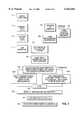
- FIG. 1is a process flow chart representing the significant steps taken to form an integrated circuit chip to substrate interconnection according to the invention.
- FIG. 2is a cross-sectional view of a portion of an integrated circuit chip having a bonding pad.
- FIG. 3is a cross-sectional view of a portion of an integrated circuit chip on which a ball bond bump is formed.
- FIGS. 4A, 4B and 4Care crosis-sectional views of a portion of an integrated circuit chip on which a coined ball bond bump is formed for use with alternative embodiments of the invention.
- FIGS. 5A and 5Bare cross-sectional views of coining tools for use with alternative embodiments of the invention.
- FIG. 6is a cross-sectional view of a portion of a substrate showing an upper surface, a conductive trace, a substrate bonding contact, and a metallization in accordance with one embodiment of the invention.
- FIG. 7is a cross-sectional view of a portion of the integrated circuit chip, disposed adjacent the substrate upper surface including the coined ball bond bump which is welded onto the metallization on the substrate bonding contact to form a metal-to-metal bond in accordance with one embodiment of the invention.
- FIG. 8is a cross-sectional view of the integrated circuit chip attached to the substrate with epoxy filling the region between the substrate and the integrated circuit chip in accordance with an alternative embodiment of the invention.
- FIG. 1is a process flow chart representing the significant steps taken to form an integrated circuit chip to substrate interconnection according to the invention.
- the process of the inventionentails preparing an integrated circuit chip (also referred to as a "chip") and a substrate separately, then attaching the integrated circuit chip to the substrate to form a partially packaged integrated circuit.
- an integrated circuit chipalso referred to as a "chip”
- semiconductor chipsare formed on a semiconductor wafer using conventional wafer fabrication techniques.
- the wafermay be of any conventional size desired and usually contains a plurality of chips.
- the internal structure of chips used for both conventional C4 applications and wire-bonding applicationsare typically the same.
- the locations of the bonding padsare different depending upon whether the chip will be used in a C4 or wire-bonding application.
- the bonding pads for a C4 application chipare nestled in the center of the chip whereas the bonding pads for a wire-bonding application chip are located along the periphery of the chip (are adjacent the edges of the chip).
- a flip chip integrated circuit chip to substrate interconnectioncan be formed using chips whose bonding pads have been patterned for use in conventional wire-bonding applications i.e. at the edges of the chip.
- FIG. 2is a cross-sectional view of a portion of an integrated circuit chip 201 (also referred to as chip 201) having a bonding pad 204 which is typically made of aluminum. As shown in FIG. 2, the passivation layer 199 is patterned to expose bonding pad 204.
- Each integrated circuit chip on the waferis then probe tested and bad chips, i.e., chips which are electrically or physically unsound; are marked or otherwise identified.
- the good chipsare "bumped" by forming a ball bond bump on predetermined bonding pads of each good chip. This process is represented by block 112 of FIG. 1. Forming ball bond bumps only on the good chips reduces the cost of producing packaged integrated circuits because time and expensive materials are not wasted on non-functioning chips.
- FIG. 3is a cross-sectional view of the portion of the integrated circuit chip 201 on which a ball bond bump 202 is formed.
- Ball bond bump 202is formed on bonding pad 204. It is to be understood that, on the entire chip 201, there are a plurality of ball bond bumps 202 formed over selected ones of the bonding pads 204 formed on chip 201.
- Ball bond bump 202may be made of, for instance: gold or a gold alloy such as gold-palladium or gold-tin; copper, or a copper alloy such as copper-tin or copper-silver; indium; antimony; palladium or palladium alloy; or hybrids of epoxy and metal in wire form.
- ball bond bumps 202are formed using a conventional wire-bonding process and a conventional wire-bonder.
- a Model 1484 wire-bonder from Kulike and Soffe of Horsham, Pa.is suitable for use with the invention.
- Ball bond bumps 202the integrated circuit chip wafer (not shown) is mounted in a bonding machine (not shown). Bond material is then fed from a capillary (not shown). Ball bond bump 202 may be formed by thermo-compression, i.e., a combination of force applied by the capillary and heat are used to form ball bond bump 202. Ball bond bump 202 may alternatively be formed thermo-sonically whereby ultrasonic energy is added to the combination of force from the capillary and heat to form-ball bond bump 202. The bond material, usually gold, or gold alloy, then becomes welded to the aluminum and forms an inter-metallic bond with the aluminum bonding pad 204. Accordingly, the method of the present invention does not require flux and there is no need for a diffusion/adhesion layer.
- ball bond bumps 202are coined to eliminate the irregularities and tails 203 of ball bond bumps 202.
- the same equipment used in the formation of ball bond bumps 202may be used to form coined ball bond bumps except that a coining tool is substituted for the capillary.
- FIGS. 4A, 4B, and 4Care cross-sectional views of coined ball bond bumps 312 according to alternative embodiments of the invention.
- the coining operationdeforms ball bond bump 202 such that coined ball bond bump 312 has a base section 302A and a generally protruding section 302B.
- a seating plane 302Cis formed on base section 302A and adjoins the base of protruding section 302B which is approximately centrally formed on seating plane 302C.
- the coined ball bond bump 312 of FIG. 4Ahas a substantially cone shaped protruding section 302B and is formed by a coining tool having a conical cross-section, such as described below with respect to Fig. 5A.
- protruding section 302B of coined ball bond bump 312has a truncated conical shape as would be formed by a coining tool such as described below with respect to FIG. 5B.
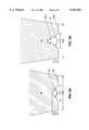
- FIGS. 5A and 5Bare cross-sectional views of coining tools 400 and 410 for use with alternative embodiments (FIGS. 4A and 4B) of the invention.
- Coining tools 400 and 410each have an indentation 401 or 411, respectively, that contacts ball bond bump 202 during the coining process.
- Indentation 401 of FIG. 5Ahas a generally conical shape.
- An interior angle 401C of indentation 401measures, in one embodiment, between 60-120° and, in another embodiment, approximately 110°.
- the width 401B of indentation 401 at base surface 400A of coining tool 400is, in one embodiment, approximately 0.002 inch (51 microns).
- the height 401A of indentation 401 from base surface 400A to the vertex of indentation interior angle 401Cis, in one embodiment, approximately 0.0007 inch (18 microns). It is to be understood that other heights 401A and widths 401B can be used.
- the indentation 411 of coining tool 410(FIG. 5B) has a truncated conical shape, i.e., a generally conical shape with a flat top.
- An interior angle 411C of indentation 411measures, in one embodiment, between 60-120° and, in another embodiment, approximately 110°.
- the width 411B of indentation 411 at base surface 410A of coining tool 410, and the height 411A of indentation 411 from base surface 410A to the flat surface 410C of indentation 411are governed by the same considerations as width 401B and height 401A of coining tool 400.
- width 411Bis approximately 0.002 inch (51 microns) and height 411A is approximately 0.0007 inch (18 microns).
- Width 411D at the truncated end of indentation 411must be smaller than width 411B. In one embodiment, width 411D is between 0.0002-0.001 inch (5-25 microns) and, in another embodiment, width 411D is approximately 0.0005 inch (13 microns).
- Coining tools having indentations with other shapescan also be used.
- the cross-section of the indentationcan have a curved shape such as a circular, elliptical or parabolic arc.
- Both coining tools 400 and 410have a circular cross-section as viewed in a direction parallel to the plane of FIGS. 5A and 5B, and perpendicular to base surfaces 400A and 410A, respectively. However, it is to be understood that the shape of this cross-section is not critical to the invention and other rounded cross-sections, such as an oval, can be used.
- the diameters 400B and 410B of base surfaces 400A and 410A, respectively,are, in one embodiment, 0.005 inch (177 microns). Diameters 400B and 410B can be any size that is small enough to avoid interference between coining tool 400 or 410 and ball bond bumps 202 adjacent the ball bond bump 202 being coined. Diameters 400B and 410B must also be larger than widths 401B and 411B of indentations 401 and 411, respectively.
- FIGS. 5A and 5Ballow for the formation of coined ball bond bumps 312 having a uniform height (Z-axis) and a precisely located center (X-axis and Y-axis) in the plane parallel to the surface of chip 201.
- Control of the geometry of coined ball bond bump 312(FIGS. 4A and 4B) is particularly advantageous and important in view of the irregular size and shape of ball bond bumps 202 obtained using conventional wire-bonding equipment.
- the height of protruding section 302B of coined ball bond bump 312 from the surface of chip 201can be controlled within a tolerance of less than 0.0002 inch (5 microns).
- the center of protruding section 302B of each coined ball bond bump 312can be located within a tolerance of 0.00008 inch (2 microns) with respect to the center of the bond pad, even if the center of un-coined ball bond bump 202 is off-center by as much as 0.001 inch (25 microns).
- chips 201can be bumped which have very fine pad to pad pitches (i.e. distances between pads of 0.004-0.005 inches). In contrast chips bumped by conventional C4 processes have pad to pad pitches which usually range from 0.008 to 0.010 inches. Controlling the geometry of the coined ball bond bumps 312 is also particularly important because fabrication tolerances must enable matching of coined ball bond bumps 312 on chip 201 to equally fine pitched patterns formed on the substrate (not shown). In the prior art, maintaining this high precision has often driven the cost of the packaged integrated circuit so high that it was not economically feasible to produce.
- FIG. 4Cis a cross-sectional view of a coined ball bond bump 312 according to a third embodiment of the invention.
- coined ball bond bump 312has a base section 302A and flat top surface 302D.
- the embodiment of FIG. 4Cis particularly well suited for low cost applications because the ball bond bumps can be coined all at once by application of a flat surface to all ball bond bumps 202 on chip 201 simultaneously, instead of applying a coining tool to each ball bond bump 202 individually as is done to form the coined ball bond bumps 312 of FIGS. 4A and 4B.
- the individually coined ball bond bumps 312 of FIGS. 4A and 4Bare preferred due to the pointed shape of the resulting coined ball bond bumps 312.
- integrated circuit chips 201 with coined ball bond bumps 312are separated by using a conventional sawing process.
- the waferis first sawn into separate chips 201.
- the good chips., i.e., electrically and physically sound chips,are then separated from the bad chips.
- Ball bond bumps 202are then formed on each of the good chips 201 and each of ball bond bumps 202 are coined, as described above, to create coined ball bond bumps 312.
- each of the chips 201are then attached to a substrate by contacting coined ball bond bumps 312 to corresponding metallizations on the substrate bonding contacts.
- a substrateis formed for use with the integrated circuit chip to substrate interconnection according to the invention.
- the substrateis made of any one of various materials such as organic laminate, ceramic, alumina, silicon, printed circuit board, thin film or flexible circuit.
- the substrateis created by a printed circuit board process.
- the substratecan include one or more layers fabricated and interconnected by methods well known by those skilled in the art.
- FIG. 6is a cross-sectional view of substrate 501 showing upper surface 501A, conductive trace 501B, substrate bonding contact 501C, and metallization 502 in accordance with the present invention.
- Conductive trace 501B and substrate bonding contact 501C on upper surface 501A of substrate 501are typically aluminum and are electrically connected to one another.
- conductive trace 501B and substrate bonding contact 501Care formed integrally, for example, are formed from the same layer of conductive material.
- Conductive trace 501B and substrate bonding contact 501Care created by methods well known in the art. It is to be understood that, on the entire substrate 501, there are a plurality of conductive traces 501B and substrate bonding contacts 501C formed on upper surface 501A.
- an isolation layer 601(FIG. 6) can be formed over substrate 501 and conductive trace 501B. As shown in FIG. 6, isolation layer 601 is patterned such that isolation layer 601 leaves uncovered a portion of substrate bonding contact 501C. Isolation layer 601 ensures that metallization 502 is applied only to substrate bonding contacts 501C. Isolation layer 601 is particularly useful when the manufacturer wants to conserve the amount of material used in forming metallization 502, such as when metallization 502 includes gold or a gold alloy.
- Isolation layer 601is a dielectric material, for example, a plating mask or a solder mask. Isolation layer 601 is applied using methods well known in the art such as dry film and etching processes, liquid film and photo-imaging processes, IBM's "SLC" process, or other known fabrication techniques.
- isolation layer 601is illustrated in FIGS. 6, 7 and 8, it is understood that step 722 in FIG. 1 is optional and that isolation layer 601 does not have to be formed.
- the metallization 502(FIG. 6) is formed on substrate bonding contact 501C.
- Metallization 502can be a multi-metal-layer metallization.
- metallization 502is formed by applying a copper layer over predetermined portions of substrate bonding contact 501C. Then a nickel layer is selectively applied over the copper layer. Finally a layer of gold or gold alloy is applied over the nickel layer.
- the thicknesses of the copper, nickel and gold layersare within the range of 200 micrometers ( ⁇ m) to 2000 ⁇ m, 100 ⁇ m to 300 ⁇ m and 10 ⁇ m to 30 ⁇ m, respectively.
- metallization 502is made of, for instance: aluminum; tin over gold over nickel over copper; tin over nickel over copper; lead over gold over tin over aluminum; or tin over lead over gold over tin over aluminum.
- Metallization 502is applied using conventional processes such as electroplating or electro-less plating.
- the substrateis next placed into a standard flip chip fixture such as the Flip Chip Aligner/Bonder available from Research Devices in West Piscataway, N.J. as Part No. M8B.
- the flip chip fixtureincludes a heater that can be used, as explained below, to heat the substrate during attachment of the chip.
- the chipis held in place above the substrate by the flip chip fixture so that the coined ball bond bumps are aligned above corresponding substrate bonding contacts.
- the substrateis then heated.
- the chipis aligned with the substrate using a vision system, as is well known in the art.
- the chipis picked up with a conventional vacuum tool (not shown).
- the vacuum tool holding the chipcan also include an optional heater which heats the chip.
- the coined ball bond bumpsare then placed into contact with the corresponding metallizations on the substrate bonding contacts.
- pressureis applied to the chip and substrate which forces the chip and substrate towards one another.
- the combination of heat and pressurecauses a weld to form between the coined ball bond bumps and the corresponding metallizations.
- the substrate and chipare heated (see block 132 of FIG. 1) to 190° centigrade (C) and 240° C., respectively.
- the substrate and chipare heated (see block 132 of FIG. 1) to 160° C. and 180° C., respectively.
- a pressure(see block 134A of FIG. 1) of about 10 grams per coined ball bond bump is applied for 10 msec.
- low level ultrasonic energycan also be applied through the vacuum tool (not shown) to vibrate the chip while the pressure is applied to the chip and substrate.
- This ultrasonic energyproduces vibration which is transmitted from the chip through the coined ball bond bumps to the corresponding metallizations and causes a weld to form between the coined ball bond bumps and the corresponding metallizations.
- the vibrationalso causes oxide layers that may be present on the surfaces of the metallizations to break up.
- the ultrasonic energy and heat applied to the chipwill also work to clean surface contamination from the coined ball bond bumps. Consequently, a better bond is formed between the metallizations and the coined ball bond bumps without the use of conventional fluxes. This is a highly advantageous feature because conventional fluxes are difficult to clean after soldering and can corrode the aluminum bonding pads.
- hydrogen gas or a hydrogen-nitrogen gas mixturecan be made to flow over the substrate, metallizations, and chip, while the coined ball bond bumps on the chip are bonded to the metallizations. This further reduces formation of surface oxides. Additionally, the metallizations can be pre-cleaned with a plasma gas to further promote effective welding.
- both coined ball bond bump 312(FIGS. 4A, 4B and 4C) and metallization 502 are made of gold.
- protruding sections 302B of coined ball bond bumps 312melt and collapse into the gold of metallizations 502 to form a welded bond.
- FIG. 7is a cross-sectional view of a portion of chip 201 disposed adjacent substrate upper surface 501A including metallization 502 and coined ball bond bump 312 which is welded onto metallization 502 on substrate bonding contact 501C to form a metal-to-metal bond 801. As shown in FIG. 7, a region 901 exists between substrate 501 and chip 201.
- the resulting bond 801is a direct gold to gold connection between coined ball bond bump 312 on chip 201 and metallization 502 on substrate bonding contact 501C on substrate 501.
- Bond 801is particularly advantageous because bond 801 is made without the use of additional solder or epoxy.
- gold-to-gold or metal-to-metal bond 801Several advantages result from the gold-to-gold or metal-to-metal bond 801 described above.
- goldis very ductile and malleable so it does not harden and crack.
- the resulting weldis not as susceptible to melting as solder, which reflows at a relatively low temperature. This is a significant advantage over my U.S. Pat. No. 5,478,007 in which solder forms part of the electrical interconnection between the chip and substrate.
- solder fluxthere is no need for applying solder flux and therefore no added risk of corrosion of the aluminum bonding pads 204 and no need to clean off residual flux or inspect for residual flux. Additionally, with the present. invention, no epoxies are required.
- bond 801is allowed to cool.
- FIG. 8is a cross-sectional view of chip 201 attached to substrate 501 with an epoxy 1001 filling the region 901 between substrate 501 and chip 201.
- epoxy 1001encloses and protects coined ball bond bump 312 from the ambient environment.
- epoxy 1001eliminates air pockets under chip 201 where moisture and contaminants can collect. Importantly, epoxy 1001 also helps relieve stress on bonds 801 between coined ball bond bumps 312 and metallizations 502.
- an encapsulantis used to enclose chip 201.
- the encapsulantencloses chip 201 so as to protect chip 201 from the ambient environment.
- the encapsulantis formed of, for instance, plastic using methods well known in the art such as injection molding, transfer molding, or potting. Use of an encapsulant to enclose chip 201 is not critical to the invention, and, in other embodiments of the invention, chip 201 may be encapsulated by other methods known to those of skill in the art.
- interconnect bumps or solder ballscan be formed on a lower surface of the substrate which is opposite the upper surface (501A) of the substrate.
- the interconnect bumps or solder ballsare formed on interconnection pads on the lower surface of the substrate.
- the interconnection padsmay be at the end of a via formed through the substrate or at the end of a trace formed on the substrate lower surface.
- the solder ballsmay be created by methods well known in the art.
- the solder ballsare used to make the electrical connection between the integrated circuit chip, the substrate, and the electrically conductive material formed on other, higher level components such as a printed circuit board.
- the substrateis placed onto the electrically conductive material of the higher level component such that the solder balls contact bonding locations on the higher level component.
- the solder ballsare then heated to reflow the solder and cooled to solidify and form a bond between the substrate and the electrically conductive material on the higher level component.
- the method of electrically connecting the substrate to the electrically conductive material on, for instance, a printed circuit boardis not part of the integrated circuit chip to substrate interconnection according to the invention and is not critical to the invention. Therefore, other methods for making this electrical connection can be employed.
- the method and apparatus of the inventionhas all the advantages of conventional flip chip (C4) interconnection. For instance, since bonding pads 204 on chip 201 are connected directly to corresponding metallizations 502 on substrate bonding contacts 501C on substrate 501 (see FIG. 8), electrical noise in signals sent to and from chip 201 is significantly reduced and the profile of a packaged integrated circuit using the integrated circuit chip to substrate interconnection of the invention can be smaller.
- chips 201 interconnected with substrate 501according to the method and apparatus of the invention, can be more densely packed in multi-chip modules (not shown). Further, by eliminating bond wires, there is no possibility of bond wire sweep.
- the method and apparatus of the inventionis considerably less expensive than conventional C4 methods because the invention uses integrated circuit chips 201 made for wire-bond interconnection, and chips used for wire-bonding applications typically cost less to make than chips processed for conventional C4 applications. Further, according to the invention, there is no need for a manufacturer to maintain separate inventories of chips for wire-bonding and flip chip applications.
- direct metal-to-metal bonds 801 between coined ball bond bumps 312 and corresponding metallizations 502, which are made in accordance with the invention (see FIGS. 7 and 8),eliminate the need to apply and/or cure additional solder or epoxy and eliminate the need to use complex photolithographic processes. This saves time, equipment and materials and avoids the corrosion and manufacturing problems associated with solders and epoxies.
Landscapes
- Engineering & Computer Science (AREA)
- Computer Hardware Design (AREA)
- Microelectronics & Electronic Packaging (AREA)
- Power Engineering (AREA)
- Wire Bonding (AREA)
Abstract
Description
Claims (7)
Priority Applications (1)
| Application Number | Priority Date | Filing Date | Title |
|---|---|---|---|
| US09/078,377US6163463A (en) | 1996-12-06 | 1998-05-13 | Integrated circuit chip to substrate interconnection |
Applications Claiming Priority (2)
| Application Number | Priority Date | Filing Date | Title |
|---|---|---|---|
| US08/761,472US5795818A (en) | 1996-12-06 | 1996-12-06 | Integrated circuit chip to substrate interconnection and method |
| US09/078,377US6163463A (en) | 1996-12-06 | 1998-05-13 | Integrated circuit chip to substrate interconnection |
Related Parent Applications (1)
| Application Number | Title | Priority Date | Filing Date |
|---|---|---|---|
| US08/761,472DivisionUS5795818A (en) | 1996-12-06 | 1996-12-06 | Integrated circuit chip to substrate interconnection and method |
Publications (1)
| Publication Number | Publication Date |
|---|---|
| US6163463Atrue US6163463A (en) | 2000-12-19 |
Family
ID=25062302
Family Applications (2)
| Application Number | Title | Priority Date | Filing Date |
|---|---|---|---|
| US08/761,472Expired - LifetimeUS5795818A (en) | 1996-12-06 | 1996-12-06 | Integrated circuit chip to substrate interconnection and method |
| US09/078,377Expired - LifetimeUS6163463A (en) | 1996-12-06 | 1998-05-13 | Integrated circuit chip to substrate interconnection |
Family Applications Before (1)
| Application Number | Title | Priority Date | Filing Date |
|---|---|---|---|
| US08/761,472Expired - LifetimeUS5795818A (en) | 1996-12-06 | 1996-12-06 | Integrated circuit chip to substrate interconnection and method |
Country Status (1)
| Country | Link |
|---|---|
| US (2) | US5795818A (en) |
Cited By (25)
| Publication number | Priority date | Publication date | Assignee | Title |
|---|---|---|---|---|
| US6277669B1 (en)* | 1999-09-15 | 2001-08-21 | Industrial Technology Research Institute | Wafer level packaging method and packages formed |
| US6309908B1 (en)* | 1999-12-21 | 2001-10-30 | Motorola, Inc. | Package for an electronic component and a method of making it |
| US20010053598A1 (en)* | 1998-11-13 | 2001-12-20 | Seiko Epson Corporation | Semiconductor device having bumps |
| US6358627B2 (en)* | 1999-04-03 | 2002-03-19 | International Business Machines Corporation | Rolling ball connector |
| US6365435B1 (en)* | 2000-12-04 | 2002-04-02 | Advanpack Solutions Pte Ltd | Method for producing a flip chip package |
| US20020151228A1 (en)* | 2001-02-27 | 2002-10-17 | Chippac, Inc. | Self-coplanarity bumping shape for flip chip |
| US6483190B1 (en)* | 1999-10-20 | 2002-11-19 | Fujitsu Limited | Semiconductor chip element, semiconductor chip element mounting structure, semiconductor chip element mounting device and mounting method |
| US6543674B2 (en)* | 2001-02-06 | 2003-04-08 | Fujitsu Limited | Multilayer interconnection and method |
| WO2002080263A3 (en)* | 2001-03-28 | 2003-09-04 | Intel Corp | Flip chip interconnection using no-clean flux |
| US6622903B1 (en)* | 2002-03-27 | 2003-09-23 | Palomar Technologies, Inc. | Production of a tailless ball bump |
| US6642079B1 (en)* | 2002-06-19 | 2003-11-04 | National Central University | Process of fabricating flip chip interconnection structure |
| US6668445B1 (en)* | 2000-01-11 | 2003-12-30 | Lexmark International, Inc. | Method of increasing tab bond strength using reactive ion etching |
| US6734570B1 (en) | 2003-01-24 | 2004-05-11 | Gennum Corporation | Solder bumped substrate for a fine pitch flip-chip integrated circuit package |
| US6740577B2 (en) | 2002-05-21 | 2004-05-25 | St Assembly Test Services Pte Ltd | Method of forming a small pitch torch bump for mounting high-performance flip-flop devices |
| US20050000727A1 (en)* | 2002-05-08 | 2005-01-06 | Sandisk Corporation | Method and apparatus for maintaining a separation between contacts |
| US20050064696A1 (en)* | 2003-09-19 | 2005-03-24 | Larson Charles E. | Methods relating to forming interconnects and resulting assemblies |
| US20060125112A1 (en)* | 2004-11-19 | 2006-06-15 | Yukihiro Ikeya | Apparatus and method for manufacturing semiconductor device |
| US20070152328A1 (en)* | 2005-12-29 | 2007-07-05 | Susheel Jadhav | Fluxless chip attached processes and devices |
| US20080254611A1 (en)* | 2002-12-17 | 2008-10-16 | Intel Corporation (A Delaware Corporation) | Interconnection designs and materials having improved strength and fatigue life |
| US20090084155A1 (en)* | 2007-09-28 | 2009-04-02 | Ryan Chase | Method to Form Pin Having Void Reducing Pin Head and Flattening Head to Perform the Method |
| US20090206480A1 (en)* | 2008-02-20 | 2009-08-20 | Atmel Corporation | Fabricating low cost solder bumps on integrated circuit wafers |
| US7700475B1 (en)* | 2006-10-05 | 2010-04-20 | Marvell International Ltd. | Pillar structure on bump pad |
| US8008130B2 (en)* | 1999-10-05 | 2011-08-30 | Renesas Electronics Corporation | Multilayer interconnection board, semiconductor device having the same, and method of forming the same as well as method of mounting the semicondutor chip on the interconnection board |
| US8220140B1 (en) | 2010-09-13 | 2012-07-17 | Western Digital (Fremont), Llc | System for performing bonding a first substrate to a second substrate |
| TWI381464B (en)* | 2008-08-29 | 2013-01-01 | Hannstar Display Corp | The bump structure and its making method |
Families Citing this family (51)
| Publication number | Priority date | Publication date | Assignee | Title |
|---|---|---|---|---|
| JP3065549B2 (en)* | 1997-01-09 | 2000-07-17 | 富士通株式会社 | Semiconductor chip component mounting method |
| US6074895A (en)* | 1997-09-23 | 2000-06-13 | International Business Machines Corporation | Method of forming a flip chip assembly |
| US6413797B2 (en) | 1997-10-09 | 2002-07-02 | Rohm Co., Ltd. | Semiconductor device and method for making the same |
| US6326241B1 (en)* | 1997-12-29 | 2001-12-04 | Visteon Global Technologies, Inc. | Solderless flip-chip assembly and method and material for same |
| US6194667B1 (en)* | 1998-08-19 | 2001-02-27 | International Business Machines Corporation | Receptor pad structure for chip carriers |
| US6130141A (en)* | 1998-10-14 | 2000-10-10 | Lucent Technologies Inc. | Flip chip metallization |
| US6138894A (en)* | 1998-11-25 | 2000-10-31 | Intermedics Inc. | Method for coupling a circuit component to a substrate |
| US6204089B1 (en)* | 1999-05-14 | 2001-03-20 | Industrial Technology Research Institute | Method for forming flip chip package utilizing cone shaped bumps |
| US6251694B1 (en)* | 1999-05-26 | 2001-06-26 | United Microelectronics Corp. | Method of testing and packaging a semiconductor chip |
| FR2795201B1 (en)* | 1999-06-15 | 2001-08-31 | Gemplus Card Int | DEVICE AND METHOD FOR MANUFACTURING ELECTRONIC DEVICES COMPRISING AT LEAST ONE CHIP FIXED ON A SUPPORT |
| JP2001093938A (en) | 1999-09-20 | 2001-04-06 | Nec Kansai Ltd | Semiconductor device and its manufacturing method |
| US6434817B1 (en)* | 1999-12-03 | 2002-08-20 | Delphi Technologies, Inc. | Method for joining an integrated circuit |
| US6442039B1 (en) | 1999-12-03 | 2002-08-27 | Delphi Technologies, Inc. | Metallic microstructure springs and method of making same |
| US20020076910A1 (en)* | 1999-12-15 | 2002-06-20 | Pace Benedict G. | High density electronic interconnection |
| US6261939B1 (en)* | 1999-12-23 | 2001-07-17 | Philips Semiconductors, Inc. | Pad metallization over active circuitry |
| JP4000743B2 (en)* | 2000-03-13 | 2007-10-31 | 株式会社デンソー | Electronic component mounting method |
| US6821888B2 (en)* | 2000-07-07 | 2004-11-23 | Chartered Semiconductor Manufacturing Ltd. | Method of copper/copper surface bonding using a conducting polymer for application in IC chip bonding |
| US6340608B1 (en) | 2000-07-07 | 2002-01-22 | Chartered Semiconductor Manufacturing Ltd. | Method of fabricating copper metal bumps for flip-chip or chip-on-board IC bonding on terminating copper pads |
| US6670214B1 (en)* | 2000-10-12 | 2003-12-30 | Lsi Logic Corporation | Insulated bonding wire for microelectronic packaging |
| US6621168B2 (en) | 2000-12-28 | 2003-09-16 | Intel Corporation | Interconnected circuit board assembly and system |
| JP3890901B2 (en)* | 2001-02-21 | 2007-03-07 | ソニー株式会社 | Electronic component mounting substrate and manufacturing method thereof |
| US6818545B2 (en)* | 2001-03-05 | 2004-11-16 | Megic Corporation | Low fabrication cost, fine pitch and high reliability solder bump |
| TWI245402B (en)* | 2002-01-07 | 2005-12-11 | Megic Corp | Rod soldering structure and manufacturing process thereof |
| US6756294B1 (en)* | 2002-01-30 | 2004-06-29 | Taiwan Semiconductor Manufacturing Company | Method for improving bump reliability for flip chip devices |
| US7253510B2 (en)* | 2003-01-16 | 2007-08-07 | International Business Machines Corporation | Ball grid array package construction with raised solder ball pads |
| US20040178498A1 (en)* | 2003-03-10 | 2004-09-16 | Low Qwai H. | Wire bonding to full array bonding pads on active circuitry |
| TWI378516B (en) | 2003-11-10 | 2012-12-01 | Chippac Inc | Bump-on-lead flip chip interconnection |
| US8026128B2 (en) | 2004-11-10 | 2011-09-27 | Stats Chippac, Ltd. | Semiconductor device and method of self-confinement of conductive bump material during reflow without solder mask |
| US8129841B2 (en) | 2006-12-14 | 2012-03-06 | Stats Chippac, Ltd. | Solder joint flip chip interconnection |
| US9029196B2 (en) | 2003-11-10 | 2015-05-12 | Stats Chippac, Ltd. | Semiconductor device and method of self-confinement of conductive bump material during reflow without solder mask |
| US8574959B2 (en) | 2003-11-10 | 2013-11-05 | Stats Chippac, Ltd. | Semiconductor device and method of forming bump-on-lead interconnection |
| US7659633B2 (en) | 2004-11-10 | 2010-02-09 | Stats Chippac, Ltd. | Solder joint flip chip interconnection having relief structure |
| US20070105277A1 (en) | 2004-11-10 | 2007-05-10 | Stats Chippac Ltd. | Solder joint flip chip interconnection |
| USRE47600E1 (en) | 2003-11-10 | 2019-09-10 | STATS ChipPAC Pte. Ltd. | Semiconductor device and method of forming electrical interconnect with stress relief void |
| US8216930B2 (en) | 2006-12-14 | 2012-07-10 | Stats Chippac, Ltd. | Solder joint flip chip interconnection having relief structure |
| US8022544B2 (en) | 2004-07-09 | 2011-09-20 | Megica Corporation | Chip structure |
| US7452803B2 (en)* | 2004-08-12 | 2008-11-18 | Megica Corporation | Method for fabricating chip structure |
| KR20070107154A (en) | 2005-03-25 | 2007-11-06 | 스태츠 칩팩, 엘티디. | Flip chip interconnects with narrow interconnect sites on the substrate |
| US8841779B2 (en) | 2005-03-25 | 2014-09-23 | Stats Chippac, Ltd. | Semiconductor device and method of forming high routing density BOL BONL and BONP interconnect sites on substrate |
| TWI330863B (en) | 2005-05-18 | 2010-09-21 | Megica Corp | Semiconductor chip with coil element over passivation layer |
| CN1901162B (en) | 2005-07-22 | 2011-04-20 | 米辑电子股份有限公司 | Method for manufacturing circuit assembly by continuous electroplating and circuit assembly structure |
| US7652374B2 (en)* | 2006-07-31 | 2010-01-26 | Chi Wah Kok | Substrate and process for semiconductor flip chip package |
| JP5134582B2 (en)* | 2009-02-13 | 2013-01-30 | 日立オートモティブシステムズ株式会社 | Connection structure and power module |
| RU2563971C2 (en) | 2010-10-14 | 2015-09-27 | Стора Энсо Ойй | Method and device of connecting chip to printed conductive surface |
| US9053989B2 (en)* | 2011-09-08 | 2015-06-09 | Taiwan Semiconductor Manufacturing Company, Ltd. | Elongated bump structure in semiconductor device |
| US9159695B2 (en) | 2013-01-07 | 2015-10-13 | Taiwan Semiconductor Manufacturing Company, Ltd. | Elongated bump structures in package structure |
| JP6780933B2 (en)* | 2015-12-18 | 2020-11-04 | 新光電気工業株式会社 | Terminal structure, terminal structure manufacturing method, and wiring board |
| JP6596469B2 (en)* | 2017-07-19 | 2019-10-23 | 株式会社フジクラ | Imaging module and manufacturing method of imaging module |
| CN108346952B (en)* | 2018-01-25 | 2020-11-24 | 番禺得意精密电子工业有限公司 | Electric connector holder |
| DE102021117573B4 (en)* | 2021-07-07 | 2023-04-13 | Tdk Electronics Ag | Method of making an electrical connection to an electronic component and a chip assembly |
| CN113835295B (en)* | 2021-09-09 | 2024-02-09 | 中国人民解放军军事科学院国防科技创新研究院 | Imprinting method of micro-nano features |
Citations (71)
| Publication number | Priority date | Publication date | Assignee | Title |
|---|---|---|---|---|
| US3373481A (en)* | 1965-06-22 | 1968-03-19 | Sperry Rand Corp | Method of electrically interconnecting conductors |
| US3429040A (en)* | 1965-06-18 | 1969-02-25 | Ibm | Method of joining a component to a substrate |
| US3488840A (en)* | 1963-12-27 | 1970-01-13 | Ibm | Method of connecting microminiaturized devices to circuit panels |
| US3838984A (en)* | 1973-04-16 | 1974-10-01 | Sperry Rand Corp | Flexible carrier and interconnect for uncased ic chips |
| US4074342A (en)* | 1974-12-20 | 1978-02-14 | International Business Machines Corporation | Electrical package for lsi devices and assembly process therefor |
| JPS57143838A (en)* | 1981-02-27 | 1982-09-06 | Mitsubishi Electric Corp | Manufacture of semiconductor device |
| JPS5897849A (en)* | 1981-12-07 | 1983-06-10 | Mitsubishi Electric Corp | Semiconductor element |
| JPS58148434A (en)* | 1982-02-26 | 1983-09-03 | Mitsubishi Electric Corp | Manufacture of electric parts mounting substrate |
| JPS58157147A (en)* | 1982-03-12 | 1983-09-19 | Mitsubishi Electric Corp | hybrid integrated circuit board |
| JPS595639A (en)* | 1982-06-30 | 1984-01-12 | Mitsubishi Electric Corp | Hybrid integrated circuit |
| JPS5931042A (en)* | 1982-08-12 | 1984-02-18 | Mitsubishi Electric Corp | High frequency high power semiconductor device |
| JPS5935439A (en)* | 1982-08-24 | 1984-02-27 | Fujitsu Ltd | How to mount a leadless chip carrier with bumps on a board |
| JPS5940539A (en)* | 1982-08-30 | 1984-03-06 | Hitachi Tobu Semiconductor Ltd | Manufacture of semiconductor device |
| JPS59208751A (en)* | 1983-05-13 | 1984-11-27 | Hitachi Ltd | Formation of bump |
| JPS6089951A (en)* | 1983-10-24 | 1985-05-20 | Nec Corp | Manufacture of flip chip ic |
| JPS6094744A (en)* | 1983-10-27 | 1985-05-27 | Nippon Denso Co Ltd | Hybrid ic device |
| US4617730A (en)* | 1984-08-13 | 1986-10-21 | International Business Machines Corporation | Method of fabricating a chip interposer |
| JPS6267829A (en)* | 1985-09-20 | 1987-03-27 | Sharp Corp | Flip chip mounting structure |
| JPS62281435A (en)* | 1986-05-30 | 1987-12-07 | Hitachi Ltd | Semiconductor device |
| JPS63164343A (en)* | 1986-12-26 | 1988-07-07 | Matsushita Electric Ind Co Ltd | Flip chip IC device |
| JPS63241955A (en)* | 1987-03-30 | 1988-10-07 | Hitachi Ltd | Manufacturing method of resin-reinforced LSI mounting structure |
| JPS63275127A (en)* | 1987-05-07 | 1988-11-11 | Matsushita Electric Ind Co Ltd | Semiconductor chip mounting body |
| JPS63288031A (en)* | 1987-05-20 | 1988-11-25 | Matsushita Electric Ind Co Ltd | Flip chip bonding |
| JPS63316447A (en)* | 1987-06-19 | 1988-12-23 | Hitachi Ltd | Semiconductor integrated circuit mounting structure |
| US4818728A (en)* | 1986-12-03 | 1989-04-04 | Sharp Kabushiki Kaisha | Method of making a hybrid semiconductor device |
| US4825284A (en)* | 1985-12-11 | 1989-04-25 | Hitachi, Ltd. | Semiconductor resin package structure |
| JPH01140766A (en)* | 1987-11-27 | 1989-06-01 | Semiconductor Energy Lab Co Ltd | Image sensor |
| JPH01161850A (en)* | 1987-12-18 | 1989-06-26 | Hitachi Ltd | Manufacturing method of semiconductor device |
| JPH01191457A (en)* | 1988-01-27 | 1989-08-01 | Fuji Electric Co Ltd | Semiconductor device |
| JPH01217936A (en)* | 1988-02-26 | 1989-08-31 | Hitachi Ltd | Manufacture of semiconductor device and apparatus thereof |
| JPH01217935A (en)* | 1988-02-26 | 1989-08-31 | Hitachi Ltd | Semiconductor device manufacturing method and device |
| JPH01243533A (en)* | 1988-03-25 | 1989-09-28 | Hitachi Ltd | Flip-chip having gourd-shaped protruding electrode |
| US4926241A (en)* | 1988-02-19 | 1990-05-15 | Microelectronics And Computer Technology Corporation | Flip substrate for chip mount |
| JPH02132836A (en)* | 1988-11-14 | 1990-05-22 | Seiko Epson Corp | semiconductor equipment |
| US4930001A (en)* | 1989-03-23 | 1990-05-29 | Hughes Aircraft Company | Alloy bonded indium bumps and methods of processing same |
| JPH02150042A (en)* | 1988-11-30 | 1990-06-08 | Nec Corp | Hybrid integrated circuit |
| JPH02189926A (en)* | 1989-01-18 | 1990-07-25 | Nec Corp | Semiconductor integrated circuit device |
| JPH02246236A (en)* | 1989-03-20 | 1990-10-02 | Fujitsu Ltd | Flip-chip bonding method |
| JPH02249248A (en)* | 1989-03-22 | 1990-10-05 | Mitsubishi Electric Corp | Manufacture of hybrid integrated circuit device |
| US4967313A (en)* | 1988-07-15 | 1990-10-30 | Contraves Ag | Electronic circuit and method of production thereof |
| US4967950A (en)* | 1989-10-31 | 1990-11-06 | International Business Machines Corporation | Soldering method |
| US4974057A (en)* | 1986-10-31 | 1990-11-27 | Texas Instruments Incorporated | Semiconductor device package with circuit board and resin |
| US5010389A (en)* | 1989-07-26 | 1991-04-23 | International Business Machines Corporation | Integrated circuit substrate with contacts thereon for a packaging structure |
| US5027188A (en)* | 1988-09-13 | 1991-06-25 | Hitachi, Ltd. | Semiconductor integrated circuit device in which a semiconductor chip is mounted with solder bumps for mounting to a wiring substrate |
| US5071787A (en)* | 1989-03-14 | 1991-12-10 | Kabushiki Kaisha Toshiba | Semiconductor device utilizing a face-down bonding and a method for manufacturing the same |
| US5088007A (en)* | 1991-04-04 | 1992-02-11 | Motorola, Inc. | Compliant solder interconnection |
| US5086966A (en)* | 1990-11-05 | 1992-02-11 | Motorola Inc. | Palladium-coated solder ball |
| US5105259A (en)* | 1990-09-28 | 1992-04-14 | Motorola, Inc. | Thermally enhanced semiconductor device utilizing a vacuum to ultimately enhance thermal dissipation |
| US5111279A (en)* | 1989-08-28 | 1992-05-05 | Lsi Logic Corp. | Apparatus for isolation of flux materials in "flip-chip" manufacturing |
| US5118370A (en)* | 1986-11-07 | 1992-06-02 | Sharp Kabushiki Kaisha | LSI chip and method of producing same |
| US5147084A (en)* | 1990-07-18 | 1992-09-15 | International Business Machines Corporation | Interconnection structure and test method |
| US5198963A (en)* | 1991-11-21 | 1993-03-30 | Motorola, Inc. | Multiple integrated circuit module which simplifies handling and testing |
| US5229647A (en)* | 1991-03-27 | 1993-07-20 | Micron Technology, Inc. | High density data storage using stacked wafers |
| US5249728A (en)* | 1993-03-10 | 1993-10-05 | Atmel Corporation | Bumpless bonding process having multilayer metallization |
| US5249450A (en)* | 1992-06-15 | 1993-10-05 | Micron Technology, Inc. | Probehead for ultrasonic forging |
| US5272111A (en)* | 1991-02-05 | 1993-12-21 | Mitsubishi Denki Kabushiki Kaisha | Method for manufacturing semiconductor device contact |
| US5289631A (en)* | 1992-03-04 | 1994-03-01 | Mcnc | Method for testing, burn-in, and/or programming of integrated circuit chips |
| US5298459A (en)* | 1988-11-21 | 1994-03-29 | Seiko Epson Corporation | Method of manufacturing semiconductor device terminal having a gold bump electrode |
| US5341979A (en)* | 1993-09-03 | 1994-08-30 | Motorola, Inc. | Method of bonding a semiconductor substrate to a support substrate and structure therefore |
| US5378869A (en)* | 1992-06-02 | 1995-01-03 | Amkor Electronics, Inc. | Method for forming an integrated circuit package with via interconnection |
| US5451274A (en)* | 1994-01-31 | 1995-09-19 | Motorola, Inc. | Reflow of multi-layer metal bumps |
| US5478007A (en)* | 1993-04-14 | 1995-12-26 | Amkor Electronics, Inc. | Method for interconnection of integrated circuit chip and substrate |
| US5559054A (en)* | 1994-12-23 | 1996-09-24 | Motorola, Inc. | Method for ball bumping a semiconductor device |
| US5587336A (en)* | 1994-12-09 | 1996-12-24 | Vlsi Technology | Bump formation on yielded semiconductor dies |
| US5633204A (en)* | 1993-11-15 | 1997-05-27 | Nec Corporation | Method and apparatus for forming bump structure used for flip-chip mounting, the bump structure and the flip-chip |
| US5659203A (en)* | 1995-06-07 | 1997-08-19 | International Business Machines Corporation | Reworkable polymer chip encapsulant |
| US5739585A (en)* | 1995-11-27 | 1998-04-14 | Micron Technology, Inc. | Single piece package for semiconductor die |
| US5757074A (en)* | 1995-07-07 | 1998-05-26 | Hughes Electronics Corporation | Microwave/millimeter wave circuit structure with discrete flip-chip mounted elements |
| US5841192A (en)* | 1994-07-21 | 1998-11-24 | Sgs-Thomson Microelectronics S.A. | Injection molded ball grid array casing |
| US5874780A (en)* | 1995-07-27 | 1999-02-23 | Nec Corporation | Method of mounting a semiconductor device to a substrate and a mounted structure |
| US5989937A (en)* | 1994-02-04 | 1999-11-23 | Lsi Logic Corporation | Method for compensating for bottom warpage of a BGA integrated circuit |
- 1996
- 1996-12-06USUS08/761,472patent/US5795818A/ennot_activeExpired - Lifetime
- 1998
- 1998-05-13USUS09/078,377patent/US6163463A/ennot_activeExpired - Lifetime
Patent Citations (72)
| Publication number | Priority date | Publication date | Assignee | Title |
|---|---|---|---|---|
| US3488840A (en)* | 1963-12-27 | 1970-01-13 | Ibm | Method of connecting microminiaturized devices to circuit panels |
| US3429040A (en)* | 1965-06-18 | 1969-02-25 | Ibm | Method of joining a component to a substrate |
| US3373481A (en)* | 1965-06-22 | 1968-03-19 | Sperry Rand Corp | Method of electrically interconnecting conductors |
| US3838984A (en)* | 1973-04-16 | 1974-10-01 | Sperry Rand Corp | Flexible carrier and interconnect for uncased ic chips |
| US4074342A (en)* | 1974-12-20 | 1978-02-14 | International Business Machines Corporation | Electrical package for lsi devices and assembly process therefor |
| JPS57143838A (en)* | 1981-02-27 | 1982-09-06 | Mitsubishi Electric Corp | Manufacture of semiconductor device |
| JPS5897849A (en)* | 1981-12-07 | 1983-06-10 | Mitsubishi Electric Corp | Semiconductor element |
| JPS58148434A (en)* | 1982-02-26 | 1983-09-03 | Mitsubishi Electric Corp | Manufacture of electric parts mounting substrate |
| JPS58157147A (en)* | 1982-03-12 | 1983-09-19 | Mitsubishi Electric Corp | hybrid integrated circuit board |
| JPS595639A (en)* | 1982-06-30 | 1984-01-12 | Mitsubishi Electric Corp | Hybrid integrated circuit |
| JPS5931042A (en)* | 1982-08-12 | 1984-02-18 | Mitsubishi Electric Corp | High frequency high power semiconductor device |
| JPS5935439A (en)* | 1982-08-24 | 1984-02-27 | Fujitsu Ltd | How to mount a leadless chip carrier with bumps on a board |
| JPS5940539A (en)* | 1982-08-30 | 1984-03-06 | Hitachi Tobu Semiconductor Ltd | Manufacture of semiconductor device |
| JPS59208751A (en)* | 1983-05-13 | 1984-11-27 | Hitachi Ltd | Formation of bump |
| JPS6089951A (en)* | 1983-10-24 | 1985-05-20 | Nec Corp | Manufacture of flip chip ic |
| JPS6094744A (en)* | 1983-10-27 | 1985-05-27 | Nippon Denso Co Ltd | Hybrid ic device |
| US4617730A (en)* | 1984-08-13 | 1986-10-21 | International Business Machines Corporation | Method of fabricating a chip interposer |
| JPS6267829A (en)* | 1985-09-20 | 1987-03-27 | Sharp Corp | Flip chip mounting structure |
| US4825284A (en)* | 1985-12-11 | 1989-04-25 | Hitachi, Ltd. | Semiconductor resin package structure |
| JPS62281435A (en)* | 1986-05-30 | 1987-12-07 | Hitachi Ltd | Semiconductor device |
| US4974057A (en)* | 1986-10-31 | 1990-11-27 | Texas Instruments Incorporated | Semiconductor device package with circuit board and resin |
| US5118370A (en)* | 1986-11-07 | 1992-06-02 | Sharp Kabushiki Kaisha | LSI chip and method of producing same |
| US4818728A (en)* | 1986-12-03 | 1989-04-04 | Sharp Kabushiki Kaisha | Method of making a hybrid semiconductor device |
| JPS63164343A (en)* | 1986-12-26 | 1988-07-07 | Matsushita Electric Ind Co Ltd | Flip chip IC device |
| JPS63241955A (en)* | 1987-03-30 | 1988-10-07 | Hitachi Ltd | Manufacturing method of resin-reinforced LSI mounting structure |
| JPS63275127A (en)* | 1987-05-07 | 1988-11-11 | Matsushita Electric Ind Co Ltd | Semiconductor chip mounting body |
| JPS63288031A (en)* | 1987-05-20 | 1988-11-25 | Matsushita Electric Ind Co Ltd | Flip chip bonding |
| JPS63316447A (en)* | 1987-06-19 | 1988-12-23 | Hitachi Ltd | Semiconductor integrated circuit mounting structure |
| JPH01140766A (en)* | 1987-11-27 | 1989-06-01 | Semiconductor Energy Lab Co Ltd | Image sensor |
| JPH01161850A (en)* | 1987-12-18 | 1989-06-26 | Hitachi Ltd | Manufacturing method of semiconductor device |
| JPH01191457A (en)* | 1988-01-27 | 1989-08-01 | Fuji Electric Co Ltd | Semiconductor device |
| US4926241A (en)* | 1988-02-19 | 1990-05-15 | Microelectronics And Computer Technology Corporation | Flip substrate for chip mount |
| JPH01217936A (en)* | 1988-02-26 | 1989-08-31 | Hitachi Ltd | Manufacture of semiconductor device and apparatus thereof |
| JPH01217935A (en)* | 1988-02-26 | 1989-08-31 | Hitachi Ltd | Semiconductor device manufacturing method and device |
| JPH01243533A (en)* | 1988-03-25 | 1989-09-28 | Hitachi Ltd | Flip-chip having gourd-shaped protruding electrode |
| US4967313A (en)* | 1988-07-15 | 1990-10-30 | Contraves Ag | Electronic circuit and method of production thereof |
| US5027188A (en)* | 1988-09-13 | 1991-06-25 | Hitachi, Ltd. | Semiconductor integrated circuit device in which a semiconductor chip is mounted with solder bumps for mounting to a wiring substrate |
| JPH02132836A (en)* | 1988-11-14 | 1990-05-22 | Seiko Epson Corp | semiconductor equipment |
| US5298459A (en)* | 1988-11-21 | 1994-03-29 | Seiko Epson Corporation | Method of manufacturing semiconductor device terminal having a gold bump electrode |
| JPH02150042A (en)* | 1988-11-30 | 1990-06-08 | Nec Corp | Hybrid integrated circuit |
| JPH02189926A (en)* | 1989-01-18 | 1990-07-25 | Nec Corp | Semiconductor integrated circuit device |
| US5071787A (en)* | 1989-03-14 | 1991-12-10 | Kabushiki Kaisha Toshiba | Semiconductor device utilizing a face-down bonding and a method for manufacturing the same |
| JPH02246236A (en)* | 1989-03-20 | 1990-10-02 | Fujitsu Ltd | Flip-chip bonding method |
| JPH02249248A (en)* | 1989-03-22 | 1990-10-05 | Mitsubishi Electric Corp | Manufacture of hybrid integrated circuit device |
| US4930001A (en)* | 1989-03-23 | 1990-05-29 | Hughes Aircraft Company | Alloy bonded indium bumps and methods of processing same |
| US5010389A (en)* | 1989-07-26 | 1991-04-23 | International Business Machines Corporation | Integrated circuit substrate with contacts thereon for a packaging structure |
| US5111279A (en)* | 1989-08-28 | 1992-05-05 | Lsi Logic Corp. | Apparatus for isolation of flux materials in "flip-chip" manufacturing |
| US4967950A (en)* | 1989-10-31 | 1990-11-06 | International Business Machines Corporation | Soldering method |
| US5147084A (en)* | 1990-07-18 | 1992-09-15 | International Business Machines Corporation | Interconnection structure and test method |
| US5105259A (en)* | 1990-09-28 | 1992-04-14 | Motorola, Inc. | Thermally enhanced semiconductor device utilizing a vacuum to ultimately enhance thermal dissipation |
| US5086966A (en)* | 1990-11-05 | 1992-02-11 | Motorola Inc. | Palladium-coated solder ball |
| US5272111A (en)* | 1991-02-05 | 1993-12-21 | Mitsubishi Denki Kabushiki Kaisha | Method for manufacturing semiconductor device contact |
| US5229647A (en)* | 1991-03-27 | 1993-07-20 | Micron Technology, Inc. | High density data storage using stacked wafers |
| US5088007A (en)* | 1991-04-04 | 1992-02-11 | Motorola, Inc. | Compliant solder interconnection |
| US5198963A (en)* | 1991-11-21 | 1993-03-30 | Motorola, Inc. | Multiple integrated circuit module which simplifies handling and testing |
| US5289631A (en)* | 1992-03-04 | 1994-03-01 | Mcnc | Method for testing, burn-in, and/or programming of integrated circuit chips |
| US5483100A (en)* | 1992-06-02 | 1996-01-09 | Amkor Electronics, Inc. | Integrated circuit package with via interconnections formed in a substrate |
| US5378869A (en)* | 1992-06-02 | 1995-01-03 | Amkor Electronics, Inc. | Method for forming an integrated circuit package with via interconnection |
| US5249450A (en)* | 1992-06-15 | 1993-10-05 | Micron Technology, Inc. | Probehead for ultrasonic forging |
| US5249728A (en)* | 1993-03-10 | 1993-10-05 | Atmel Corporation | Bumpless bonding process having multilayer metallization |
| US5478007A (en)* | 1993-04-14 | 1995-12-26 | Amkor Electronics, Inc. | Method for interconnection of integrated circuit chip and substrate |
| US5341979A (en)* | 1993-09-03 | 1994-08-30 | Motorola, Inc. | Method of bonding a semiconductor substrate to a support substrate and structure therefore |
| US5633204A (en)* | 1993-11-15 | 1997-05-27 | Nec Corporation | Method and apparatus for forming bump structure used for flip-chip mounting, the bump structure and the flip-chip |
| US5451274A (en)* | 1994-01-31 | 1995-09-19 | Motorola, Inc. | Reflow of multi-layer metal bumps |
| US5989937A (en)* | 1994-02-04 | 1999-11-23 | Lsi Logic Corporation | Method for compensating for bottom warpage of a BGA integrated circuit |
| US5841192A (en)* | 1994-07-21 | 1998-11-24 | Sgs-Thomson Microelectronics S.A. | Injection molded ball grid array casing |
| US5587336A (en)* | 1994-12-09 | 1996-12-24 | Vlsi Technology | Bump formation on yielded semiconductor dies |
| US5559054A (en)* | 1994-12-23 | 1996-09-24 | Motorola, Inc. | Method for ball bumping a semiconductor device |
| US5659203A (en)* | 1995-06-07 | 1997-08-19 | International Business Machines Corporation | Reworkable polymer chip encapsulant |
| US5757074A (en)* | 1995-07-07 | 1998-05-26 | Hughes Electronics Corporation | Microwave/millimeter wave circuit structure with discrete flip-chip mounted elements |
| US5874780A (en)* | 1995-07-27 | 1999-02-23 | Nec Corporation | Method of mounting a semiconductor device to a substrate and a mounted structure |
| US5739585A (en)* | 1995-11-27 | 1998-04-14 | Micron Technology, Inc. | Single piece package for semiconductor die |
Non-Patent Citations (10)
| Title |
|---|
| Becher, et al., "Direct Chip Attach (DCA), The Introduction of New Packaging Concept for Portable Electronics", Motorola et al., Presented in the 1993 IEPS Proceedings pp. 519-533. |
| Becher, et al., Direct Chip Attach (DCA), The Introduction of New Packaging Concept for Portable Electronics , Motorola et al., Presented in the 1993 IEPS Proceedings pp. 519 533.* |
| Chance, D., Metallurgical System For C4 Joint BLM, IBM Technical Bulletin, vol. 27, No. 9, Feb. 1985, p. 5212.* |
| Eldring, J. et al., "Flip Chip Attach of Silicon and GaAs Fine Pitch Devices As Well As Inner Lead Tab Attach Using Ball Bump Technology", Technical Univ. of Berlin, Presented in the 1993 IEPS Proceedings, pp 304-320. |
| Eldring, J. et al., Flip Chip Attach of Silicon and GaAs Fine Pitch Devices As Well As Inner Lead Tab Attach Using Ball Bump Technology , Technical Univ. of Berlin, Presented in the 1993 IEPS Proceedings, pp 304 320.* |
| Encapsulated Solder Joint For Chip Mounting, IBM Technical Disclosure Bulletin, vol. 32, No. 10B, Mar. 1990, p. 480.* |
| Harman, George G., "Wire Bonding in Microelectronics", National Institute of Standards and Technology, ©1989, 1991 International Society of Hybrid Microelectronics, ISBN 0-930815-25-4; Chapter 2, pp. 49-94. |
| Harman, George G., Wire Bonding in Microelectronics , National Institute of Standards and Technology, 1989, 1991 International Society of Hybrid Microelectronics, ISBN 0 930815 25 4; Chapter 2, pp. 49 94.* |
| Koopman, N. et al., "Chip-To-Package Interconnections," MicroElectronics Packaging Handbook, 1989, Chapter 6, pp. 361-391. |
| Koopman, N. et al., Chip To Package Interconnections, MicroElectronics Packaging Handbook, 1989, Chapter 6, pp. 361 391.* |
Cited By (46)
| Publication number | Priority date | Publication date | Assignee | Title |
|---|---|---|---|---|
| US20010053598A1 (en)* | 1998-11-13 | 2001-12-20 | Seiko Epson Corporation | Semiconductor device having bumps |
| US6689679B2 (en)* | 1998-11-13 | 2004-02-10 | Seiko Epson Corporation | Semiconductor device having bumps |
| US6358627B2 (en)* | 1999-04-03 | 2002-03-19 | International Business Machines Corporation | Rolling ball connector |
| US6277669B1 (en)* | 1999-09-15 | 2001-08-21 | Industrial Technology Research Institute | Wafer level packaging method and packages formed |
| US8008130B2 (en)* | 1999-10-05 | 2011-08-30 | Renesas Electronics Corporation | Multilayer interconnection board, semiconductor device having the same, and method of forming the same as well as method of mounting the semicondutor chip on the interconnection board |
| US6483190B1 (en)* | 1999-10-20 | 2002-11-19 | Fujitsu Limited | Semiconductor chip element, semiconductor chip element mounting structure, semiconductor chip element mounting device and mounting method |
| US20030057552A1 (en)* | 1999-10-20 | 2003-03-27 | Fujitsu Limited | Semiconductor chip element, semiconductor chip element mounting structure, semiconductor chip element mounting device and mounting method |
| US7436062B2 (en)* | 1999-10-20 | 2008-10-14 | Fujitsu Limited | Semiconductor chip element, semiconductor chip element mounting structure, semiconductor chip element mounting device and mounting method |
| US6309908B1 (en)* | 1999-12-21 | 2001-10-30 | Motorola, Inc. | Package for an electronic component and a method of making it |
| US6668445B1 (en)* | 2000-01-11 | 2003-12-30 | Lexmark International, Inc. | Method of increasing tab bond strength using reactive ion etching |
| US6365435B1 (en)* | 2000-12-04 | 2002-04-02 | Advanpack Solutions Pte Ltd | Method for producing a flip chip package |
| US6543674B2 (en)* | 2001-02-06 | 2003-04-08 | Fujitsu Limited | Multilayer interconnection and method |
| US20050221535A1 (en)* | 2001-02-27 | 2005-10-06 | Chippac, Inc. | Method for making self-coplanarity bumping shape for flip chip |
| US7211901B2 (en)* | 2001-02-27 | 2007-05-01 | Chippac, Inc. | Self-coplanarity bumping shape for flip chip |
| US20020151228A1 (en)* | 2001-02-27 | 2002-10-17 | Chippac, Inc. | Self-coplanarity bumping shape for flip chip |
| US20050218515A1 (en)* | 2001-02-27 | 2005-10-06 | Chippac, Inc | Self-coplanarity bumping shape for flip chip |
| US7407877B2 (en) | 2001-02-27 | 2008-08-05 | Chippac, Inc. | Self-coplanarity bumping shape for flip-chip |
| US6940178B2 (en)* | 2001-02-27 | 2005-09-06 | Chippac, Inc. | Self-coplanarity bumping shape for flip chip |
| US6713318B2 (en) | 2001-03-28 | 2004-03-30 | Intel Corporation | Flip chip interconnection using no-clean flux |
| US20040152238A1 (en)* | 2001-03-28 | 2004-08-05 | Michihisa Maeda | Flip chip interconnection using no-clean flux |
| WO2002080263A3 (en)* | 2001-03-28 | 2003-09-04 | Intel Corp | Flip chip interconnection using no-clean flux |
| US6622903B1 (en)* | 2002-03-27 | 2003-09-23 | Palomar Technologies, Inc. | Production of a tailless ball bump |
| US20050000727A1 (en)* | 2002-05-08 | 2005-01-06 | Sandisk Corporation | Method and apparatus for maintaining a separation between contacts |
| US7138583B2 (en)* | 2002-05-08 | 2006-11-21 | Sandisk Corporation | Method and apparatus for maintaining a separation between contacts |
| US6740577B2 (en) | 2002-05-21 | 2004-05-25 | St Assembly Test Services Pte Ltd | Method of forming a small pitch torch bump for mounting high-performance flip-flop devices |
| US6642079B1 (en)* | 2002-06-19 | 2003-11-04 | National Central University | Process of fabricating flip chip interconnection structure |
| US8642462B2 (en)* | 2002-12-17 | 2014-02-04 | Micorn Technology, Inc. | Interconnection designs and materials having improved strength and fatigue life |
| US20080254611A1 (en)* | 2002-12-17 | 2008-10-16 | Intel Corporation (A Delaware Corporation) | Interconnection designs and materials having improved strength and fatigue life |
| US9136239B2 (en) | 2002-12-17 | 2015-09-15 | Micron Technology, Inc. | Interconnection designs and materials having improved strength and fatigue life |
| US6734570B1 (en) | 2003-01-24 | 2004-05-11 | Gennum Corporation | Solder bumped substrate for a fine pitch flip-chip integrated circuit package |
| US7208410B2 (en) | 2003-09-19 | 2007-04-24 | Micron Technology, Inc. | Methods relating to forming interconnects |
| US6982191B2 (en) | 2003-09-19 | 2006-01-03 | Micron Technology, Inc. | Methods relating to forming interconnects and resulting assemblies |
| US7208839B2 (en) | 2003-09-19 | 2007-04-24 | Micron Technology, Inc. | Semiconductor component assemblies having interconnects |
| US20060160274A1 (en)* | 2003-09-19 | 2006-07-20 | Larson Charles E | Methods relating to forming interconnects |
| US20050064696A1 (en)* | 2003-09-19 | 2005-03-24 | Larson Charles E. | Methods relating to forming interconnects and resulting assemblies |
| US20050200008A1 (en)* | 2003-09-19 | 2005-09-15 | Larson Charles E. | Methods relating to forming interconnects and resulting assemblies |
| US20060125112A1 (en)* | 2004-11-19 | 2006-06-15 | Yukihiro Ikeya | Apparatus and method for manufacturing semiconductor device |
| US7534715B2 (en)* | 2005-12-29 | 2009-05-19 | Intel Corporation | Methods including fluxless chip attach processes |
| US20070152328A1 (en)* | 2005-12-29 | 2007-07-05 | Susheel Jadhav | Fluxless chip attached processes and devices |
| US7700475B1 (en)* | 2006-10-05 | 2010-04-20 | Marvell International Ltd. | Pillar structure on bump pad |
| US7999395B1 (en) | 2006-10-05 | 2011-08-16 | Marvell International Ltd. | Pillar structure on bump pad |
| US20090084155A1 (en)* | 2007-09-28 | 2009-04-02 | Ryan Chase | Method to Form Pin Having Void Reducing Pin Head and Flattening Head to Perform the Method |
| US20090206480A1 (en)* | 2008-02-20 | 2009-08-20 | Atmel Corporation | Fabricating low cost solder bumps on integrated circuit wafers |
| TWI381464B (en)* | 2008-08-29 | 2013-01-01 | Hannstar Display Corp | The bump structure and its making method |
| US8220140B1 (en) | 2010-09-13 | 2012-07-17 | Western Digital (Fremont), Llc | System for performing bonding a first substrate to a second substrate |
| US8763235B1 (en) | 2010-09-13 | 2014-07-01 | Western Digital (Fremont), Llc | Method for bonding substrates in an energy assisted magnetic recording head |
Also Published As
| Publication number | Publication date |
|---|---|
| US5795818A (en) | 1998-08-18 |
Similar Documents
| Publication | Publication Date | Title |
|---|---|---|
| US6163463A (en) | Integrated circuit chip to substrate interconnection | |
| US5478007A (en) | Method for interconnection of integrated circuit chip and substrate | |
| USRE39603E1 (en) | Process for manufacturing semiconductor device and semiconductor wafer | |
| US6414382B1 (en) | Film carrier tape, semiconductor assembly, semiconductor device and method of manufacturing the same, mounted board, and electronic instrument | |
| JP2570637B2 (en) | MCM carrier | |
| US6043564A (en) | Semiconductor device having ball-bonded pads | |
| US5950070A (en) | Method of forming a chip scale package, and a tool used in forming the chip scale package | |
| US5942795A (en) | Leaded substrate carrier for integrated circuit device and leaded substrate carrier device assembly | |
| JP3481444B2 (en) | Semiconductor device and manufacturing method thereof | |
| US6165887A (en) | Method of improving interconnect of semiconductor devices by using a flattened ball bond | |
| KR0137826B1 (en) | Package method and device package | |
| US4949224A (en) | Structure for mounting a semiconductor device | |
| US6310395B1 (en) | Electronic component with anodically bonded contact | |
| JP5497392B2 (en) | Semiconductor device | |
| KR20030055130A (en) | Semiconductor device and manufacturing method of the same | |
| US5113314A (en) | High-speed, high-density chip mounting | |
| US5569956A (en) | Interposer connecting leadframe and integrated circuit | |
| KR20010069987A (en) | Semiconductor Device | |
| US20040072396A1 (en) | Semiconductor electronic device and method of manufacturing thereof | |
| KR100198682B1 (en) | Semiconductor device manufacturing method | |
| US5054680A (en) | Bonding electrical conductors | |
| JPH11186440A (en) | Semiconductor device | |
| KR20090069382A (en) | Semiconductor package | |
| JP2000012621A (en) | Semiconductor device and method of manufacturing the same | |
| JPH04127547A (en) | Lsi mounting structure |
Legal Events
| Date | Code | Title | Description |
|---|---|---|---|
| AS | Assignment | Owner name:AMKOR TECHNOLOGY, INC., ARIZONA Free format text:MERGER;ASSIGNOR:AMKOR ELECTRONICS, INC.;REEL/FRAME:009269/0987 Effective date:19980414 | |
| AS | Assignment | Owner name:SOCIETE GENERALE, NEW YORK Free format text:SECURITY INTEREST;ASSIGNORS:AMKOR TECHNOLOGY, INC.;GUARDIAN ASSETS, INC.;REEL/FRAME:011491/0917 Effective date:20000428 | |
| STCF | Information on status: patent grant | Free format text:PATENTED CASE | |
| AS | Assignment | Owner name:CITICORP USA, INC., NEW YORK Free format text:SECURITY INTEREST;ASSIGNORS:SOCIETE GENERALE;GUARDIAN ASSETS, INC.;REEL/FRAME:011682/0416 Effective date:20010330 Owner name:CITICORP USA, INC., NEW YORK Free format text:SECURITY INTEREST;ASSIGNOR:AMKOR TECHNOLOGY, INC.;REEL/FRAME:011712/0623 Effective date:20010330 | |
| CC | Certificate of correction | ||
| FEPP | Fee payment procedure | Free format text:PAYOR NUMBER ASSIGNED (ORIGINAL EVENT CODE: ASPN); ENTITY STATUS OF PATENT OWNER: LARGE ENTITY | |
| FPAY | Fee payment | Year of fee payment:4 | |
| AS | Assignment | Owner name:CITICORP NORTH AMERICA, INC. AS ADMINISTRATIVE AGE Free format text:SECURITY AGREEMENT;ASSIGNORS:AMKOR TECHNOLOGY, INC.;GUARDIAN ASSETS, INC.;REEL/FRAME:014885/0691 Effective date:20040629 | |
| AS | Assignment | Owner name:AMKOR TECHNOLOGY, INC., PENNSYLVANIA Free format text:RELEASE OF LIEN ON PATENTS;ASSIGNOR:CITICORP USA, INC. AS COLLATERAL AGENT;REEL/FRAME:015603/0572 Effective date:20040629 | |
| AS | Assignment | Owner name:CITICORP NORTH AMERICA, INC. AS "AGENT", NEW YORK Free format text:SECURITY AGREEMENT;ASSIGNORS:AMKOR TECHNOLOGY, INC.;GUARDIAN ASSETS, INC.;REEL/FRAME:015942/0521 Effective date:20041027 | |
| AS | Assignment | Owner name:AMKOR TECHNOLOGY, INC., ARIZONA Free format text:TERMINATION & RELEASE OF PATENT SECURITY AGREEMENT;ASSIGNOR:CITICORP NORTH AMERICA, INC.;REEL/FRAME:017388/0868 Effective date:20051128 Owner name:BANK OF AMERICA, N.A., TEXAS Free format text:SECURITY AGREEMENT;ASSIGNOR:AMKOR TECHNOLOGY, INC.;REEL/FRAME:017379/0630 Effective date:20051123 | |
| FPAY | Fee payment | Year of fee payment:8 | |
| FPAY | Fee payment | Year of fee payment:12 | |
| AS | Assignment | Owner name:BANK OF AMERICA, N.A., AS AGENT, CALIFORNIA Free format text:SECURITY INTEREST;ASSIGNOR:AMKOR TECHNOLOGY, INC.;REEL/FRAME:046683/0139 Effective date:20180713 | |
| AS | Assignment | Owner name:AMKOR TECHNOLOGY SINGAPORE HOLDING PTE.LTD., SINGAPORE Free format text:ASSIGNMENT OF ASSIGNORS INTEREST;ASSIGNOR:AMKOR TECHNOLOGY, INC.;REEL/FRAME:054036/0599 Effective date:20191119 |