US6163307A - Multilayered helical antenna for mobile telecommunication units - Google Patents
Multilayered helical antenna for mobile telecommunication unitsDownload PDFInfo
- Publication number
- US6163307A US6163307AUS09/401,468US40146899AUS6163307AUS 6163307 AUS6163307 AUS 6163307AUS 40146899 AUS40146899 AUS 40146899AUS 6163307 AUS6163307 AUS 6163307A
- Authority
- US
- United States
- Prior art keywords
- helical antenna
- hole
- dielectric
- partially opened
- antenna
- Prior art date
- Legal status (The legal status is an assumption and is not a legal conclusion. Google has not performed a legal analysis and makes no representation as to the accuracy of the status listed.)
- Expired - Lifetime
Links
- 239000004020conductorSubstances0.000claimsabstractdescription20
- 230000010287polarizationEffects0.000claimsabstractdescription7
- 238000010295mobile communicationMethods0.000claimsabstract2
- 230000005404monopoleEffects0.000claimsdescription4
- 238000004891communicationMethods0.000claimsdescription2
- 239000003989dielectric materialSubstances0.000claimsdescription2
- 230000005855radiationEffects0.000description3
- 239000010949copperSubstances0.000description2
- RYGMFSIKBFXOCR-UHFFFAOYSA-NCopperChemical compound[Cu]RYGMFSIKBFXOCR-UHFFFAOYSA-N0.000description1
- BQCADISMDOOEFD-UHFFFAOYSA-NSilverChemical compound[Ag]BQCADISMDOOEFD-UHFFFAOYSA-N0.000description1
- 229910052802copperInorganic materials0.000description1
- 230000007423decreaseEffects0.000description1
- -1e.g.Substances0.000description1
- 238000004519manufacturing processMethods0.000description1
- 238000000034methodMethods0.000description1
- 238000012986modificationMethods0.000description1
- 230000004048modificationEffects0.000description1
- 229910052709silverInorganic materials0.000description1
- 239000004332silverSubstances0.000description1
- 238000004804windingMethods0.000description1
Images


Classifications
- H—ELECTRICITY
- H01—ELECTRIC ELEMENTS
- H01Q—ANTENNAS, i.e. RADIO AERIALS
- H01Q1/00—Details of, or arrangements associated with, antennas
- H01Q1/36—Structural form of radiating elements, e.g. cone, spiral, umbrella; Particular materials used therewith
- H—ELECTRICITY
- H01—ELECTRIC ELEMENTS
- H01Q—ANTENNAS, i.e. RADIO AERIALS
- H01Q11/00—Electrically-long antennas having dimensions more than twice the shortest operating wavelength and consisting of conductive active radiating elements
- H01Q11/02—Non-resonant antennas, e.g. travelling-wave antenna
- H01Q11/08—Helical antennas
- H—ELECTRICITY
- H01—ELECTRIC ELEMENTS
- H01Q—ANTENNAS, i.e. RADIO AERIALS
- H01Q1/00—Details of, or arrangements associated with, antennas
- H01Q1/12—Supports; Mounting means
- H01Q1/22—Supports; Mounting means by structural association with other equipment or articles
- H01Q1/24—Supports; Mounting means by structural association with other equipment or articles with receiving set
- H01Q1/241—Supports; Mounting means by structural association with other equipment or articles with receiving set used in mobile communications, e.g. GSM
- H01Q1/242—Supports; Mounting means by structural association with other equipment or articles with receiving set used in mobile communications, e.g. GSM specially adapted for hand-held use
- H—ELECTRICITY
- H01—ELECTRIC ELEMENTS
- H01Q—ANTENNAS, i.e. RADIO AERIALS
- H01Q1/00—Details of, or arrangements associated with, antennas
- H01Q1/36—Structural form of radiating elements, e.g. cone, spiral, umbrella; Particular materials used therewith
- H01Q1/362—Structural form of radiating elements, e.g. cone, spiral, umbrella; Particular materials used therewith for broadside radiating helical antennas
- H—ELECTRICITY
- H01—ELECTRIC ELEMENTS
- H01Q—ANTENNAS, i.e. RADIO AERIALS
- H01Q1/00—Details of, or arrangements associated with, antennas
- H01Q1/36—Structural form of radiating elements, e.g. cone, spiral, umbrella; Particular materials used therewith
- H01Q1/38—Structural form of radiating elements, e.g. cone, spiral, umbrella; Particular materials used therewith formed by a conductive layer on an insulating support
Definitions
- the present inventionrelates to an antenna for transmitting and receiving radio frequency signals; and, more particularly, to a multilayered helical antenna for use in mobile telecommunication units, the antenna incorporating therein a plurality of dielectric sheets, wherein the dielectric sheets some of which are each provided with a conductor pattern are stacked on top of each other.
- a helical antennais provided with a dielectric body and an elongated metallic conductor having an appropriate length and spirally or helically wound therearound.
- the helical antennaincludes a dielectric body 30 having a through-hole 40 at center thereof, and a metallic coil 10 or a metallic conductor pattern 20 spirally or helically wound on the dielectric body 30, whereby a power is fed through a coaxial line thereof.
- the helical antennaincludes a monopole antenna 50 extendibly and receivably inserted into the through-hole 40 to thereby allow it to be used as a retractable antenna.
- a main beamis axially established along the spiral direction.
- the main beamis established perpendicular to an axis of the antenna.
- Such a antennais known as a normal-mode helical antenna("NMHA").
- NMHAnormal-mode helical antenna
- a current pathcorresponds to a total length of the conductor.
- the current path thereofis extremely large in comparison to a vertical length of the antenna, i.e., usually a multiple of ten times the vertical length, allowing the helical antenna to exhibit excellent radiation resistance characteristics.
- the radiation resistanceincreases, upto a limit, in proportion to a square of the length of the conductor path increased, the limit being one wavelength.
- the radiation resistancedecreases.
- a winding number and a turn radius of the spiral conductor in the helical antennacannot be indefinitely increased and they must be appropriately balanced in order to provide the optimum performance.
- a multilayered helical antennafor use in mobile telecommunication units comprising a first dielectric sheet provided with a through-hole at a center thereof; a plurality of second dielectric sheets, all of the second dielectric sheets, except one, being provided with a starting hole and an ending hole, the exception having second dielectric sheet having only one starting hole, each being provided with a partially opened circular metallic pattern and a through-hole at a center thereof, wherein the partially opened circular metallic pattern extends from the starting hole to the ending hole in the respective second dielectric sheet except for the dielectric sheet having the starting hole only where the partially opened circular metallic pattern extends from the starting hole to a free end; and a plurality of third dielectric sheets, each being provided with via hole and a through-hole at a center thereof, wherein the dielectric sheets are stacked in a predetermined order, the order being that the first dielectric sheet is placed at top of the stack followed by the second dielectric sheet with the starting hole only followed by the third dielectric sheet
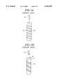
- FIGS. 1A and 1Brepresent a fragmentary exploded view of a conventional helical antenna
- FIG. 2sets forth an exploded perspective view of a structure of a multilayered antenna in accordance with a preferred embodiment of the present invention
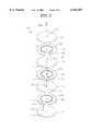
- FIGS. 3A to 3Cpresent plan views of a multilayered antenna for illustrating a helical conductor pattern
- FIG. 4illustrates a perspective view of a spiral conductor of the multilayered helical antenna shown in FIG. 2;
- FIG. 5depicts a partial cross sectional view of an inventive multilayered antenna mounted on a radio mobile station.
- the inventive multilayered helical antenna 100includes a first dielectric sheet 130, a plurality of second dielectric sheets 120 and a plurality of third dielectric sheets 110.
- Each of the dielectric sheets 110 to 130has a substantially disc shape and is made of a dielectric material having a predetermined dielectric constant and is provided with a through-hole 180 at a center thereof, allowing a whip antenna 200 to be slid upward and downward along a center axis of the helical antenna 100 which is formed by stacking the dielectric sheets in a predetermined order, the order being that the first dielectric sheet 130 is placed at top of the stack followed by the second dielectric sheet 120 followed by the third dielectric sheet 110 followed by the second dielectric sheet 120 followed by the third dielectric sheet 110 and so on, with the third dielectric sheet 110 being placed at bottom of the stack.
- each of the dielectric sheets 120 and 130may be formed in a predetermined thickness or each thereof may be formed by a plurality of dielectric sheets to obtain the predetermined thickness.
- All of the second dielectric sheets 120are each provided with a starting hole 122 and an ending hole 124, with an exception having only one starting hole 122.
- the second dielectric sheet with the one starting hole 122 onlyis always placed right below the first dielectric sheet 130. It may be that the starting holes 122 and the ending holes 124 have a diameter of about 0.4 mm.
- Each of the third dielectric sheets 110is provided with a via hole 112.
- each of the second dielectric sheets 120is provided with a partially opened circular metallic pattern 132, made of a conducting material, e.g., silver (Ag) or copper (Cu), formed in the same rotating direction.
- the partially opened circular metallic pattern 132 of the second dielectric sheets 120 positioned right above the third dielectric sheet 110 located at bottom of the stackextends from the starting holes 122 to the ending hole 124 with an arc angle ⁇ 1 between the holes 122 and 124 as shown in FIG. 3A.
- the partially opened circular metallic pattern 132 of the successive second dielectric sheet 110is formed in the same manner as the partially opened circular metallic pattern 132 of the previous second dielectric sheet 120 with an arc angle ⁇ 2 between the holes 122 and 124 as shown in FIG. 3B.
- the circular metallic pattern 132 of the second dielectric sheet 120 located right below the first dielectric sheet 130extends from the starting hole 122 to a free end thereof with an arc angle ⁇ 3 between the starting hole 122 and the free end thereof as shown in FIG. 3C. It is preferable that the arc angles of ⁇ 3 is substantially equal or smaller than that of ⁇ 1 and ⁇ 2 and ⁇ 1 and ⁇ 2 are equal to each other.
- a pattern thickness, an inner diameter, an outer diameter and a pattern width of each the partially opened circular metallic patterns 132may be changed depending on a frequency band used and are, in case of a personal communication system(PCS) utilizing the frequency band of 1.8 GHz, are approximately 0.4 mm, 4.5 to 5 mm, 5 to 5.5 mm and approximately 0.4 to 0.45 mm, respectively.
- PCSpersonal communication system
- the via hole 112 of the third dielectric sheet 110 located at bottom of the stackcorresponds to the starting hole 122 of the second dielectric sheet 120 located thereabove
- that of the second dielectric sheet 120 located above the second dielectric sheet located above the third dielectric sheet 110 at bottom of the stackcorresponds to the starting hole 122 of the second dielectric sheet 120 and the closing hole 124 of the third dielectric sheet 110 located below the first dielectric sheet 130
- that of the third dielectric sheet 110corresponds to the starting hole 122 of the second dielectric sheet 120 located below the first dielectric sheet 130 and the starting hole 124 of the second dielectric sheet 120 located therebelow.
- the via holes 112are filled with the same conducting material 142 as the partially opened circular metallic patterns to thereby vertically connect the partially opened circular metallic patterns 132 on the second dielectric sheets 120 through the corresponding starting holes 122 and ending holes 124.
- the partially opened circular patterns 132When the partially opened circular patterns 132 are vertically connected through the conducting material 142 in the via holes 112 and the starting and the ending holes 122 and 124, a spiral is formed as shown in FIG. 4, allowing it to transmit and receive horizontal and vertical polarizations. That is, the partially opened circular metallic patterns 132 maintain circles in the horizontal direction to thereby form a conventional helical antenna structure, while the conducting materials 142 in the via holes 112 form a conventional monopole antenna structure in the vertical direction, thereby providing the inventive antenna with an omnidirectional antenna characteristic capable of transmitting and receiving the horizontal and vertical polarizations.
- the total length of the spiral shown in FIG. 4is ⁇ /4 at a desired operating center frequency and may be selectively controlled depending on the dielectric constant of the dielectric sheet.
- the helical antennamay be constructed using the spiral having 2.5 turns, i.e., two and a half partially opened circular metallic patterns, and for use at 1.2 GHz, 4 turns. Further, it is preferable that each of the partially opened circular metallic patterns 132 are as close to a circle of 360° as possible in order to transmit and receive horizontal polarizations, but usually include the opening of 5 to 15°.
- dielectric sheets 110 to 130 as described aboveare integrated through a stacking process at a high temperature and a high pressure to form the helical antenna 100 as illustrated in FIG. 5.
- a height of the helical antenna 100may be changed depending on the frequency being used, the length of the partially opened circular metallic patterns 132 and the depth of the via holes 112, i.e., thickness of the dielectric sheets, since a vertical element of the helical antenna 100 is formed by the conducting material 142 filling the via holes 112.
- the height thereof for use as a mobile telecommunication antennais approximately 5 to 15 mm.
- the inventive multilayered antennaincludes a helical antenna 100 with a through-hole 180 at a center thereof and mounted on a coaxial feeder 310 of a unit body 300 and a whip antenna 200, which is a metallic monopole antenna, disposed movably along the center axis, i.e., of the helical antenna 100.
- a diameter of the through-hole 180can be varied depending on that of the whip antenna 200, and, in general, is 2.5 to 3 mm.
- a length of the whip antenna 200is basically a multiple of ⁇ /8, but it may be selectively varied.
- a feeding terminal 102 formed on a lower portion of the whip antenna 200comes in contact with the coaxial feeder 310 of the unit 300.
- a voltageis applied through the feeding terminal 120 from a matching circuit (not shown) to the whip antenna 200 in such a way that a power is fed to the whip antenna 200.
- the helical antenna 100is fixed to the coaxial feeder 310, the power is fed to helical antenna 100 regardless of whether the power is fed to the whip antenna 200 or not.
- the whip antenna 200when the whip antenna 200 is pushed inside the unit 300 through the center of the helical antenna 100, the feeding terminal 102 formed on a lower portion of the whip antenna 200 is electrically disconnected from the coaxial feeder 310 of the unit 300. As a result, a voltage cannot be applied to the whip antenna 200 and consequently the whip antenna 200 becomes inoperational and the helical antenna 100 only operates to transmit and receive a signal.
- the helical antenna of the present inventioncan transmit and receive the horizontal and the vertical polarizations by itself. Further, since the spiral patterns are formed directly on the dielectric sheets, it is possible that the manufacturing processes becomes simpler.
Landscapes
- Engineering & Computer Science (AREA)
- Computer Networks & Wireless Communication (AREA)
- Details Of Aerials (AREA)
- Support Of Aerials (AREA)
Abstract
Description
Claims (13)
Applications Claiming Priority (2)
| Application Number | Priority Date | Filing Date | Title |
|---|---|---|---|
| KR98-52315 | 1998-12-01 | ||
| KR1019980052315AKR100275279B1 (en) | 1998-12-01 | 1998-12-01 | Stacked helical antenna |
Publications (1)
| Publication Number | Publication Date |
|---|---|
| US6163307Atrue US6163307A (en) | 2000-12-19 |
Family
ID=19560817
Family Applications (1)
| Application Number | Title | Priority Date | Filing Date |
|---|---|---|---|
| US09/401,468Expired - LifetimeUS6163307A (en) | 1998-12-01 | 1999-09-22 | Multilayered helical antenna for mobile telecommunication units |
Country Status (3)
| Country | Link |
|---|---|
| US (1) | US6163307A (en) |
| KR (1) | KR100275279B1 (en) |
| CN (1) | CN1199314C (en) |
Cited By (40)
| Publication number | Priority date | Publication date | Assignee | Title |
|---|---|---|---|---|
| US6333722B1 (en)* | 1999-06-08 | 2001-12-25 | Nec Corporation | Helical antenna with adjoining insulator units |
| US6448934B1 (en)* | 2001-06-15 | 2002-09-10 | Hewlett-Packard Company | Multi band antenna |
| US6738650B1 (en)* | 2000-11-28 | 2004-05-18 | Motorola, Inc. | Radiation shielding tri-band antenna adapted to provide dual band polarizations |
| US20040095289A1 (en)* | 2002-07-04 | 2004-05-20 | Meerae Tech, Inc. | Multi-band helical antenna |
| US20060290577A1 (en)* | 2005-06-09 | 2006-12-28 | Mete Ozkar | Retractable stubby antenna |
| WO2008063026A1 (en)* | 2006-11-23 | 2008-05-29 | E.M.W. Antenna Co., Ltd. | Antenna of parallel-ring type |
| WO2008084999A1 (en)* | 2007-01-11 | 2008-07-17 | E.M.W. Antenna Co., Ltd. | Integrated antenna of parallel-ring type |
| US20130069843A1 (en)* | 2009-03-09 | 2013-03-21 | Nucurrent Inc. | Method of Operation of a Multi-Layer-Multi-Turn Structure for High Efficiency Wireless Communication |
| CN104882667A (en)* | 2015-04-27 | 2015-09-02 | 北京理工大学 | A Multilayer Quadrifilar Helical Antenna System |
| US9208942B2 (en) | 2009-03-09 | 2015-12-08 | Nucurrent, Inc. | Multi-layer-multi-turn structure for high efficiency wireless communication |
| US9300046B2 (en) | 2009-03-09 | 2016-03-29 | Nucurrent, Inc. | Method for manufacture of multi-layer-multi-turn high efficiency inductors |
| US9306358B2 (en) | 2009-03-09 | 2016-04-05 | Nucurrent, Inc. | Method for manufacture of multi-layer wire structure for high efficiency wireless communication |
| US9439287B2 (en) | 2009-03-09 | 2016-09-06 | Nucurrent, Inc. | Multi-layer wire structure for high efficiency wireless communication |
| US9444213B2 (en) | 2009-03-09 | 2016-09-13 | Nucurrent, Inc. | Method for manufacture of multi-layer wire structure for high efficiency wireless communication |
| US20170317423A1 (en)* | 2014-10-20 | 2017-11-02 | Ruag Space Ab | Multifilar helix antenna |
| US9941590B2 (en) | 2015-08-07 | 2018-04-10 | Nucurrent, Inc. | Single structure multi mode antenna for wireless power transmission using magnetic field coupling having magnetic shielding |
| US9941729B2 (en) | 2015-08-07 | 2018-04-10 | Nucurrent, Inc. | Single layer multi mode antenna for wireless power transmission using magnetic field coupling |
| US9941743B2 (en) | 2015-08-07 | 2018-04-10 | Nucurrent, Inc. | Single structure multi mode antenna having a unitary body construction for wireless power transmission using magnetic field coupling |
| US9948129B2 (en) | 2015-08-07 | 2018-04-17 | Nucurrent, Inc. | Single structure multi mode antenna for wireless power transmission using magnetic field coupling having an internal switch circuit |
| US9960628B2 (en) | 2015-08-07 | 2018-05-01 | Nucurrent, Inc. | Single structure multi mode antenna having a single layer structure with coils on opposing sides for wireless power transmission using magnetic field coupling |
| US9960629B2 (en) | 2015-08-07 | 2018-05-01 | Nucurrent, Inc. | Method of operating a single structure multi mode antenna for wireless power transmission using magnetic field coupling |
| US10063100B2 (en) | 2015-08-07 | 2018-08-28 | Nucurrent, Inc. | Electrical system incorporating a single structure multimode antenna for wireless power transmission using magnetic field coupling |
| US10424969B2 (en) | 2016-12-09 | 2019-09-24 | Nucurrent, Inc. | Substrate configured to facilitate through-metal energy transfer via near field magnetic coupling |
| US10636563B2 (en) | 2015-08-07 | 2020-04-28 | Nucurrent, Inc. | Method of fabricating a single structure multi mode antenna for wireless power transmission using magnetic field coupling |
| US10658847B2 (en) | 2015-08-07 | 2020-05-19 | Nucurrent, Inc. | Method of providing a single structure multi mode antenna for wireless power transmission using magnetic field coupling |
| US10879704B2 (en) | 2016-08-26 | 2020-12-29 | Nucurrent, Inc. | Wireless connector receiver module |
| US10903688B2 (en) | 2017-02-13 | 2021-01-26 | Nucurrent, Inc. | Wireless electrical energy transmission system with repeater |
| US10985465B2 (en) | 2015-08-19 | 2021-04-20 | Nucurrent, Inc. | Multi-mode wireless antenna configurations |
| US11056922B1 (en) | 2020-01-03 | 2021-07-06 | Nucurrent, Inc. | Wireless power transfer system for simultaneous transfer to multiple devices |
| US11152151B2 (en) | 2017-05-26 | 2021-10-19 | Nucurrent, Inc. | Crossover coil structure for wireless transmission |
| US11205848B2 (en) | 2015-08-07 | 2021-12-21 | Nucurrent, Inc. | Method of providing a single structure multi mode antenna having a unitary body construction for wireless power transmission using magnetic field coupling |
| US11227712B2 (en) | 2019-07-19 | 2022-01-18 | Nucurrent, Inc. | Preemptive thermal mitigation for wireless power systems |
| US11271430B2 (en) | 2019-07-19 | 2022-03-08 | Nucurrent, Inc. | Wireless power transfer system with extended wireless charging range |
| US11283303B2 (en) | 2020-07-24 | 2022-03-22 | Nucurrent, Inc. | Area-apportioned wireless power antenna for maximized charging volume |
| US11336003B2 (en) | 2009-03-09 | 2022-05-17 | Nucurrent, Inc. | Multi-layer, multi-turn inductor structure for wireless transfer of power |
| US20220200342A1 (en) | 2020-12-22 | 2022-06-23 | Nucurrent, Inc. | Ruggedized communication for wireless power systems in multi-device environments |
| US11695302B2 (en) | 2021-02-01 | 2023-07-04 | Nucurrent, Inc. | Segmented shielding for wide area wireless power transmitter |
| US11831174B2 (en) | 2022-03-01 | 2023-11-28 | Nucurrent, Inc. | Cross talk and interference mitigation in dual wireless power transmitter |
| US11876386B2 (en) | 2020-12-22 | 2024-01-16 | Nucurrent, Inc. | Detection of foreign objects in large charging volume applications |
| US12003116B2 (en) | 2022-03-01 | 2024-06-04 | Nucurrent, Inc. | Wireless power transfer system for simultaneous transfer to multiple devices with cross talk and interference mitigation |
Families Citing this family (6)
| Publication number | Priority date | Publication date | Assignee | Title |
|---|---|---|---|---|
| KR100400062B1 (en)* | 2000-12-02 | 2003-09-29 | 조주대 | Wireless helix antenna manufacturing method |
| KR100398826B1 (en)* | 2000-12-02 | 2003-09-19 | 미래테크 주식회사 | Wireless helix antenna manufacturing method |
| KR20020085622A (en)* | 2001-05-09 | 2002-11-16 | 조주대 | Wireless helix antenna manufacturing method and antenna therefrom |
| KR100589699B1 (en)* | 2002-07-04 | 2006-06-15 | (주)안테나 텍 | Multiband Stackable Helical Antenna |
| KR100705540B1 (en)* | 2002-07-04 | 2007-04-09 | (주)안테나 텍 | Multiband Stackable Helical Antenna |
| KR100589696B1 (en)* | 2002-07-04 | 2006-06-15 | (주)안테나 텍 | Multiband Stackable Helical Antenna |
Citations (7)
| Publication number | Priority date | Publication date | Assignee | Title |
|---|---|---|---|---|
| US5798737A (en)* | 1995-09-05 | 1998-08-25 | Murata Mfg. Co., Ltd. | Chip antenna |
| US5861852A (en)* | 1996-04-16 | 1999-01-19 | Murata Mfg. Co. Ltd. | Chip antenna |
| US5933116A (en)* | 1996-06-05 | 1999-08-03 | Murata Manufacturing Co., Ltd. | Chip antenna |
| US5977927A (en)* | 1996-02-07 | 1999-11-02 | Murata Manufacturing Co., Ltd. | Chip antenna |
| US6028568A (en)* | 1997-12-11 | 2000-02-22 | Murata Manufacturing Co., Ltd. | Chip-antenna |
| US6031496A (en)* | 1996-08-06 | 2000-02-29 | Ik-Products Oy | Combination antenna |
| US6069592A (en)* | 1996-06-15 | 2000-05-30 | Allgon Ab | Meander antenna device |
Family Cites Families (1)
| Publication number | Priority date | Publication date | Assignee | Title |
|---|---|---|---|---|
| KR100213373B1 (en)* | 1996-05-28 | 1999-08-02 | 이형도 | An antenna for wireless lan card |
- 1998
- 1998-12-01KRKR1019980052315Apatent/KR100275279B1/ennot_activeExpired - Fee Related
- 1999
- 1999-09-22USUS09/401,468patent/US6163307A/ennot_activeExpired - Lifetime
- 1999-12-01CNCNB991255372Apatent/CN1199314C/ennot_activeExpired - Fee Related
Patent Citations (7)
| Publication number | Priority date | Publication date | Assignee | Title |
|---|---|---|---|---|
| US5798737A (en)* | 1995-09-05 | 1998-08-25 | Murata Mfg. Co., Ltd. | Chip antenna |
| US5977927A (en)* | 1996-02-07 | 1999-11-02 | Murata Manufacturing Co., Ltd. | Chip antenna |
| US5861852A (en)* | 1996-04-16 | 1999-01-19 | Murata Mfg. Co. Ltd. | Chip antenna |
| US5933116A (en)* | 1996-06-05 | 1999-08-03 | Murata Manufacturing Co., Ltd. | Chip antenna |
| US6069592A (en)* | 1996-06-15 | 2000-05-30 | Allgon Ab | Meander antenna device |
| US6031496A (en)* | 1996-08-06 | 2000-02-29 | Ik-Products Oy | Combination antenna |
| US6028568A (en)* | 1997-12-11 | 2000-02-22 | Murata Manufacturing Co., Ltd. | Chip-antenna |
Cited By (104)
| Publication number | Priority date | Publication date | Assignee | Title |
|---|---|---|---|---|
| US6333722B1 (en)* | 1999-06-08 | 2001-12-25 | Nec Corporation | Helical antenna with adjoining insulator units |
| US6738650B1 (en)* | 2000-11-28 | 2004-05-18 | Motorola, Inc. | Radiation shielding tri-band antenna adapted to provide dual band polarizations |
| US6448934B1 (en)* | 2001-06-15 | 2002-09-10 | Hewlett-Packard Company | Multi band antenna |
| US20040095289A1 (en)* | 2002-07-04 | 2004-05-20 | Meerae Tech, Inc. | Multi-band helical antenna |
| US6897830B2 (en)* | 2002-07-04 | 2005-05-24 | Antenna Tech, Inc. | Multi-band helical antenna |
| US20060290577A1 (en)* | 2005-06-09 | 2006-12-28 | Mete Ozkar | Retractable stubby antenna |
| US7224316B2 (en)* | 2005-06-09 | 2007-05-29 | Kyocera Wireless Corp. | Retractable stubby antenna |
| WO2008063026A1 (en)* | 2006-11-23 | 2008-05-29 | E.M.W. Antenna Co., Ltd. | Antenna of parallel-ring type |
| WO2008084999A1 (en)* | 2007-01-11 | 2008-07-17 | E.M.W. Antenna Co., Ltd. | Integrated antenna of parallel-ring type |
| KR100861880B1 (en) | 2007-01-11 | 2008-10-09 | 주식회사 이엠따블유안테나 | Built-in antenna with parallel-ring structure |
| US20100134360A1 (en)* | 2007-01-11 | 2010-06-03 | Byung Hoon Ryou | Integrated antenna of parallel-ring type |
| US9444213B2 (en) | 2009-03-09 | 2016-09-13 | Nucurrent, Inc. | Method for manufacture of multi-layer wire structure for high efficiency wireless communication |
| US11916400B2 (en) | 2009-03-09 | 2024-02-27 | Nucurrent, Inc. | Multi-layer-multi-turn structure for high efficiency wireless communication |
| US9208942B2 (en) | 2009-03-09 | 2015-12-08 | Nucurrent, Inc. | Multi-layer-multi-turn structure for high efficiency wireless communication |
| US9232893B2 (en)* | 2009-03-09 | 2016-01-12 | Nucurrent, Inc. | Method of operation of a multi-layer-multi-turn structure for high efficiency wireless communication |
| US9300046B2 (en) | 2009-03-09 | 2016-03-29 | Nucurrent, Inc. | Method for manufacture of multi-layer-multi-turn high efficiency inductors |
| US9306358B2 (en) | 2009-03-09 | 2016-04-05 | Nucurrent, Inc. | Method for manufacture of multi-layer wire structure for high efficiency wireless communication |
| US9439287B2 (en) | 2009-03-09 | 2016-09-06 | Nucurrent, Inc. | Multi-layer wire structure for high efficiency wireless communication |
| US20130069843A1 (en)* | 2009-03-09 | 2013-03-21 | Nucurrent Inc. | Method of Operation of a Multi-Layer-Multi-Turn Structure for High Efficiency Wireless Communication |
| US11336003B2 (en) | 2009-03-09 | 2022-05-17 | Nucurrent, Inc. | Multi-layer, multi-turn inductor structure for wireless transfer of power |
| US12316128B2 (en) | 2009-03-09 | 2025-05-27 | Nucurrent, Inc. | Multi-layer-multi-turn structure for high efficiency wireless communication |
| US11335999B2 (en) | 2009-03-09 | 2022-05-17 | Nucurrent, Inc. | Device having a multi-layer-multi-turn antenna with frequency |
| US11476566B2 (en) | 2009-03-09 | 2022-10-18 | Nucurrent, Inc. | Multi-layer-multi-turn structure for high efficiency wireless communication |
| US20170317423A1 (en)* | 2014-10-20 | 2017-11-02 | Ruag Space Ab | Multifilar helix antenna |
| US10079433B2 (en)* | 2014-10-20 | 2018-09-18 | Ruag Space Ab | Multifilar helix antenna |
| CN104882667A (en)* | 2015-04-27 | 2015-09-02 | 北京理工大学 | A Multilayer Quadrifilar Helical Antenna System |
| US11205848B2 (en) | 2015-08-07 | 2021-12-21 | Nucurrent, Inc. | Method of providing a single structure multi mode antenna having a unitary body construction for wireless power transmission using magnetic field coupling |
| US9941729B2 (en) | 2015-08-07 | 2018-04-10 | Nucurrent, Inc. | Single layer multi mode antenna for wireless power transmission using magnetic field coupling |
| US9941743B2 (en) | 2015-08-07 | 2018-04-10 | Nucurrent, Inc. | Single structure multi mode antenna having a unitary body construction for wireless power transmission using magnetic field coupling |
| US11469598B2 (en) | 2015-08-07 | 2022-10-11 | Nucurrent, Inc. | Device having a multimode antenna with variable width of conductive wire |
| US9948129B2 (en) | 2015-08-07 | 2018-04-17 | Nucurrent, Inc. | Single structure multi mode antenna for wireless power transmission using magnetic field coupling having an internal switch circuit |
| US9960628B2 (en) | 2015-08-07 | 2018-05-01 | Nucurrent, Inc. | Single structure multi mode antenna having a single layer structure with coils on opposing sides for wireless power transmission using magnetic field coupling |
| US10636563B2 (en) | 2015-08-07 | 2020-04-28 | Nucurrent, Inc. | Method of fabricating a single structure multi mode antenna for wireless power transmission using magnetic field coupling |
| US10658847B2 (en) | 2015-08-07 | 2020-05-19 | Nucurrent, Inc. | Method of providing a single structure multi mode antenna for wireless power transmission using magnetic field coupling |
| US9941590B2 (en) | 2015-08-07 | 2018-04-10 | Nucurrent, Inc. | Single structure multi mode antenna for wireless power transmission using magnetic field coupling having magnetic shielding |
| US11769629B2 (en) | 2015-08-07 | 2023-09-26 | Nucurrent, Inc. | Device having a multimode antenna with variable width of conductive wire |
| US10063100B2 (en) | 2015-08-07 | 2018-08-28 | Nucurrent, Inc. | Electrical system incorporating a single structure multimode antenna for wireless power transmission using magnetic field coupling |
| US11025070B2 (en) | 2015-08-07 | 2021-06-01 | Nucurrent, Inc. | Device having a multimode antenna with at least one conductive wire with a plurality of turns |
| US11955809B2 (en) | 2015-08-07 | 2024-04-09 | Nucurrent, Inc. | Single structure multi mode antenna for wireless power transmission incorporating a selection circuit |
| US11196266B2 (en) | 2015-08-07 | 2021-12-07 | Nucurrent, Inc. | Device having a multimode antenna with conductive wire width |
| US12136514B2 (en) | 2015-08-07 | 2024-11-05 | Nucurrent, Inc. | Device having a multimode antenna with variable width of conductive wire |
| US9960629B2 (en) | 2015-08-07 | 2018-05-01 | Nucurrent, Inc. | Method of operating a single structure multi mode antenna for wireless power transmission using magnetic field coupling |
| US11205849B2 (en) | 2015-08-07 | 2021-12-21 | Nucurrent, Inc. | Multi-coil antenna structure with tunable inductance |
| US12155132B2 (en) | 2015-08-19 | 2024-11-26 | Nucurrent, Inc. | Multi-mode wireless antenna configurations |
| US11670856B2 (en) | 2015-08-19 | 2023-06-06 | Nucurrent, Inc. | Multi-mode wireless antenna configurations |
| US11316271B2 (en) | 2015-08-19 | 2022-04-26 | Nucurrent, Inc. | Multi-mode wireless antenna configurations |
| US10985465B2 (en) | 2015-08-19 | 2021-04-20 | Nucurrent, Inc. | Multi-mode wireless antenna configurations |
| US10897140B2 (en) | 2016-08-26 | 2021-01-19 | Nucurrent, Inc. | Method of operating a wireless connector system |
| US10903660B2 (en) | 2016-08-26 | 2021-01-26 | Nucurrent, Inc. | Wireless connector system circuit |
| US12327931B2 (en) | 2016-08-26 | 2025-06-10 | Nucurrent, Inc. | Wireless connector system |
| US11011915B2 (en) | 2016-08-26 | 2021-05-18 | Nucurrent, Inc. | Method of making a wireless connector transmitter module |
| US10879704B2 (en) | 2016-08-26 | 2020-12-29 | Nucurrent, Inc. | Wireless connector receiver module |
| US10938220B2 (en) | 2016-08-26 | 2021-03-02 | Nucurrent, Inc. | Wireless connector system |
| US10931118B2 (en) | 2016-08-26 | 2021-02-23 | Nucurrent, Inc. | Wireless connector transmitter module with an electrical connector |
| US10916950B2 (en) | 2016-08-26 | 2021-02-09 | Nucurrent, Inc. | Method of making a wireless connector receiver module |
| US10879705B2 (en) | 2016-08-26 | 2020-12-29 | Nucurrent, Inc. | Wireless connector receiver module with an electrical connector |
| US10886751B2 (en) | 2016-08-26 | 2021-01-05 | Nucurrent, Inc. | Wireless connector transmitter module |
| US11764614B2 (en) | 2016-12-09 | 2023-09-19 | Nucurrent, Inc. | Method of fabricating an antenna having a substrate configured to facilitate through-metal energy transfer via near field magnetic coupling |
| US10868444B2 (en) | 2016-12-09 | 2020-12-15 | Nucurrent, Inc. | Method of operating a system having a substrate configured to facilitate through-metal energy transfer via near field magnetic coupling |
| US10424969B2 (en) | 2016-12-09 | 2019-09-24 | Nucurrent, Inc. | Substrate configured to facilitate through-metal energy transfer via near field magnetic coupling |
| US10432031B2 (en) | 2016-12-09 | 2019-10-01 | Nucurrent, Inc. | Antenna having a substrate configured to facilitate through-metal energy transfer via near field magnetic coupling |
| US12136828B2 (en) | 2016-12-09 | 2024-11-05 | Nucurrent, Inc. | Method of fabricating an antenna having a substrate configured to facilitate through-metal energy transfer via near field magnetic coupling |
| US10892646B2 (en) | 2016-12-09 | 2021-01-12 | Nucurrent, Inc. | Method of fabricating an antenna having a substrate configured to facilitate through-metal energy transfer via near field magnetic coupling |
| US11418063B2 (en) | 2016-12-09 | 2022-08-16 | Nucurrent, Inc. | Method of fabricating an antenna having a substrate configured to facilitate through-metal energy transfer via near field magnetic coupling |
| US10432032B2 (en) | 2016-12-09 | 2019-10-01 | Nucurrent, Inc. | Wireless system having a substrate configured to facilitate through-metal energy transfer via near field magnetic coupling |
| US10432033B2 (en) | 2016-12-09 | 2019-10-01 | Nucurrent, Inc. | Electronic device having a sidewall configured to facilitate through-metal energy transfer via near field magnetic coupling |
| US11264837B2 (en) | 2017-02-13 | 2022-03-01 | Nucurrent, Inc. | Transmitting base with antenna having magnetic shielding panes |
| US11177695B2 (en) | 2017-02-13 | 2021-11-16 | Nucurrent, Inc. | Transmitting base with magnetic shielding and flexible transmitting antenna |
| US11223235B2 (en) | 2017-02-13 | 2022-01-11 | Nucurrent, Inc. | Wireless electrical energy transmission system |
| US10958105B2 (en) | 2017-02-13 | 2021-03-23 | Nucurrent, Inc. | Transmitting base with repeater |
| US11223234B2 (en) | 2017-02-13 | 2022-01-11 | Nucurrent, Inc. | Method of operating a wireless electrical energy transmission base |
| US11431200B2 (en) | 2017-02-13 | 2022-08-30 | Nucurrent, Inc. | Method of operating a wireless electrical energy transmission system |
| US12166360B2 (en) | 2017-02-13 | 2024-12-10 | Nucurrent, Inc. | Method of operating a wireless electrical energy transmission system |
| US10903688B2 (en) | 2017-02-13 | 2021-01-26 | Nucurrent, Inc. | Wireless electrical energy transmission system with repeater |
| US11502547B2 (en) | 2017-02-13 | 2022-11-15 | Nucurrent, Inc. | Wireless electrical energy transmission system with transmitting antenna having magnetic field shielding panes |
| US11705760B2 (en) | 2017-02-13 | 2023-07-18 | Nucurrent, Inc. | Method of operating a wireless electrical energy transmission system |
| US11282638B2 (en) | 2017-05-26 | 2022-03-22 | Nucurrent, Inc. | Inductor coil structures to influence wireless transmission performance |
| US11283295B2 (en) | 2017-05-26 | 2022-03-22 | Nucurrent, Inc. | Device orientation independent wireless transmission system |
| US11652511B2 (en) | 2017-05-26 | 2023-05-16 | Nucurrent, Inc. | Inductor coil structures to influence wireless transmission performance |
| US11152151B2 (en) | 2017-05-26 | 2021-10-19 | Nucurrent, Inc. | Crossover coil structure for wireless transmission |
| US11283296B2 (en) | 2017-05-26 | 2022-03-22 | Nucurrent, Inc. | Crossover inductor coil and assembly for wireless transmission |
| US12199699B2 (en) | 2017-05-26 | 2025-01-14 | Nucurrent, Inc. | Inductor coil structures to influence wireless transmission performance |
| US11277029B2 (en) | 2017-05-26 | 2022-03-15 | Nucurrent, Inc. | Multi coil array for wireless energy transfer with flexible device orientation |
| US11277028B2 (en) | 2017-05-26 | 2022-03-15 | Nucurrent, Inc. | Wireless electrical energy transmission system for flexible device orientation |
| US12368000B2 (en) | 2019-07-19 | 2025-07-22 | Nucurrent, Inc. | Wireless power transfer system with extended wireless charging range |
| US11756728B2 (en) | 2019-07-19 | 2023-09-12 | Nucurrent, Inc. | Wireless power transfer system with extended wireless charging range |
| US11227712B2 (en) | 2019-07-19 | 2022-01-18 | Nucurrent, Inc. | Preemptive thermal mitigation for wireless power systems |
| US11271430B2 (en) | 2019-07-19 | 2022-03-08 | Nucurrent, Inc. | Wireless power transfer system with extended wireless charging range |
| US11811223B2 (en) | 2020-01-03 | 2023-11-07 | Nucurrent, Inc. | Wireless power transfer system for simultaneous transfer to multiple devices |
| US12278501B2 (en) | 2020-01-03 | 2025-04-15 | Nucurrent, Inc. | Wireless power transfer system for simultaneous transfer to multiple devices |
| US11056922B1 (en) | 2020-01-03 | 2021-07-06 | Nucurrent, Inc. | Wireless power transfer system for simultaneous transfer to multiple devices |
| US11658517B2 (en) | 2020-07-24 | 2023-05-23 | Nucurrent, Inc. | Area-apportioned wireless power antenna for maximized charging volume |
| US11283303B2 (en) | 2020-07-24 | 2022-03-22 | Nucurrent, Inc. | Area-apportioned wireless power antenna for maximized charging volume |
| US12027881B2 (en) | 2020-07-24 | 2024-07-02 | Nucurrent, Inc. | Area-apportioned wireless power antenna for maximized charging volume |
| US12316137B2 (en) | 2020-07-24 | 2025-05-27 | Nucurrent, Inc. | Area-apportioned wireless power antenna for maximized charging volume |
| US11881716B2 (en) | 2020-12-22 | 2024-01-23 | Nucurrent, Inc. | Ruggedized communication for wireless power systems in multi-device environments |
| US11876386B2 (en) | 2020-12-22 | 2024-01-16 | Nucurrent, Inc. | Detection of foreign objects in large charging volume applications |
| US12199452B2 (en) | 2020-12-22 | 2025-01-14 | Nucurrent, Inc. | Detection of foreign objects in large charging volume applications |
| US20220200342A1 (en) | 2020-12-22 | 2022-06-23 | Nucurrent, Inc. | Ruggedized communication for wireless power systems in multi-device environments |
| US11996706B2 (en) | 2021-02-01 | 2024-05-28 | Nucurrent, Inc. | Segmented shielding for wide area wireless power transmitter |
| US11695302B2 (en) | 2021-02-01 | 2023-07-04 | Nucurrent, Inc. | Segmented shielding for wide area wireless power transmitter |
| US12142940B2 (en) | 2022-03-01 | 2024-11-12 | Nucurrent, Inc. | Cross talk and interference mitigation in dual wireless power transmitter |
| US11831174B2 (en) | 2022-03-01 | 2023-11-28 | Nucurrent, Inc. | Cross talk and interference mitigation in dual wireless power transmitter |
| US12003116B2 (en) | 2022-03-01 | 2024-06-04 | Nucurrent, Inc. | Wireless power transfer system for simultaneous transfer to multiple devices with cross talk and interference mitigation |
Also Published As
| Publication number | Publication date |
|---|---|
| KR100275279B1 (en) | 2000-12-15 |
| CN1199314C (en) | 2005-04-27 |
| CN1257322A (en) | 2000-06-21 |
| HK1026072A1 (en) | 2000-12-01 |
| KR20000017675A (en) | 2000-04-06 |
Similar Documents
| Publication | Publication Date | Title |
|---|---|---|
| US6163307A (en) | Multilayered helical antenna for mobile telecommunication units | |
| KR100414765B1 (en) | Ceramic chip antenna | |
| US5990848A (en) | Combined structure of a helical antenna and a dielectric plate | |
| US6897830B2 (en) | Multi-band helical antenna | |
| JP3662591B2 (en) | Combined multi-segment helical antenna | |
| US5945963A (en) | Dielectrically loaded antenna and a handheld radio communication unit including such an antenna | |
| EP0747989B1 (en) | Double-action antenna | |
| EP1263081B1 (en) | Helical antenna | |
| US6639560B1 (en) | Single feed tri-band PIFA with parasitic element | |
| EP0706231A1 (en) | Antenna equipment | |
| Tawk et al. | The miniaturization of a partially 3-D printed quadrifilar helix antenna | |
| JPH10224139A (en) | Dual frequency antenna | |
| WO2004019450A1 (en) | Apparatus and method for forming a monolithic surface-mountable antenna | |
| WO2003041216A2 (en) | Dual band spiral-shaped antenna | |
| WO2002095875A1 (en) | Dual band dipole antenna structure | |
| US6448934B1 (en) | Multi band antenna | |
| US5933116A (en) | Chip antenna | |
| EP3314694A1 (en) | Multi-filar helical antenna | |
| EP0828310A2 (en) | Antenna device | |
| JP2020184712A (en) | Helical antenna and antenna device | |
| WO2001020715A1 (en) | Antenna device and communication terminal comprising the same | |
| EP2242143A1 (en) | Antenna with increased electrical length and wireless communication device including the same | |
| WO1997027642A1 (en) | ANTENNA FOR FREQUENCIES IN EXCESS OF 200 MHz | |
| JP4195038B2 (en) | Dual band antenna | |
| KR100589699B1 (en) | Multiband Stackable Helical Antenna |
Legal Events
| Date | Code | Title | Description |
|---|---|---|---|
| AS | Assignment | Owner name:KOREA ELECTRONICS TECHNOLOGY INSTITUTE, KOREA, REP Free format text:ASSIGNMENT OF ASSIGNORS INTEREST;ASSIGNORS:KIM, JONG KYU;PARK, IN SHIG;SEO, HO SEOK;REEL/FRAME:010279/0553 Effective date:19990908 | |
| FEPP | Fee payment procedure | Free format text:PAYOR NUMBER ASSIGNED (ORIGINAL EVENT CODE: ASPN); ENTITY STATUS OF PATENT OWNER: SMALL ENTITY | |
| STCF | Information on status: patent grant | Free format text:PATENTED CASE | |
| FPAY | Fee payment | Year of fee payment:4 | |
| FPAY | Fee payment | Year of fee payment:8 | |
| FEPP | Fee payment procedure | Free format text:PAYER NUMBER DE-ASSIGNED (ORIGINAL EVENT CODE: RMPN); ENTITY STATUS OF PATENT OWNER: SMALL ENTITY Free format text:PAYOR NUMBER ASSIGNED (ORIGINAL EVENT CODE: ASPN); ENTITY STATUS OF PATENT OWNER: SMALL ENTITY | |
| FPAY | Fee payment | Year of fee payment:12 | |
| AS | Assignment | Owner name:INTELLECTUAL DISCOVERY CO., LTD., KOREA, REPUBLIC Free format text:LICENSE;ASSIGNOR:KOREA ELECTRONICS TECHNOLOGY INSTITUTE;REEL/FRAME:032551/0669 Effective date:20140328 |