US6161915A - Identification of thermal inkjet printer cartridges - Google Patents
Identification of thermal inkjet printer cartridgesDownload PDFInfo
- Publication number
- US6161915A US6161915AUS09/099,814US9981498AUS6161915AUS 6161915 AUS6161915 AUS 6161915AUS 9981498 AUS9981498 AUS 9981498AUS 6161915 AUS6161915 AUS 6161915A
- Authority
- US
- United States
- Prior art keywords
- printer
- circuit
- wires
- cartridge
- electrically
- Prior art date
- Legal status (The legal status is an assumption and is not a legal conclusion. Google has not performed a legal analysis and makes no representation as to the accuracy of the status listed.)
- Expired - Lifetime
Links
Images


Classifications
- B—PERFORMING OPERATIONS; TRANSPORTING
- B41—PRINTING; LINING MACHINES; TYPEWRITERS; STAMPS
- B41J—TYPEWRITERS; SELECTIVE PRINTING MECHANISMS, i.e. MECHANISMS PRINTING OTHERWISE THAN FROM A FORME; CORRECTION OF TYPOGRAPHICAL ERRORS
- B41J2/00—Typewriters or selective printing mechanisms characterised by the printing or marking process for which they are designed
- B41J2/005—Typewriters or selective printing mechanisms characterised by the printing or marking process for which they are designed characterised by bringing liquid or particles selectively into contact with a printing material
- B41J2/01—Ink jet
- B41J2/17—Ink jet characterised by ink handling
- B41J2/175—Ink supply systems ; Circuit parts therefor
- B41J2/17503—Ink cartridges
- B41J2/17543—Cartridge presence detection or type identification
- B41J2/17546—Cartridge presence detection or type identification electronically
- H—ELECTRICITY
- H05—ELECTRIC TECHNIQUES NOT OTHERWISE PROVIDED FOR
- H05K—PRINTED CIRCUITS; CASINGS OR CONSTRUCTIONAL DETAILS OF ELECTRIC APPARATUS; MANUFACTURE OF ASSEMBLAGES OF ELECTRICAL COMPONENTS
- H05K1/00—Printed circuits
- H05K1/02—Details
- H05K1/0266—Marks, test patterns or identification means
- H—ELECTRICITY
- H05—ELECTRIC TECHNIQUES NOT OTHERWISE PROVIDED FOR
- H05K—PRINTED CIRCUITS; CASINGS OR CONSTRUCTIONAL DETAILS OF ELECTRIC APPARATUS; MANUFACTURE OF ASSEMBLAGES OF ELECTRICAL COMPONENTS
- H05K3/00—Apparatus or processes for manufacturing printed circuits
- H05K3/36—Assembling printed circuits with other printed circuits
- H05K3/361—Assembling flexible printed circuits with other printed circuits
- Y—GENERAL TAGGING OF NEW TECHNOLOGICAL DEVELOPMENTS; GENERAL TAGGING OF CROSS-SECTIONAL TECHNOLOGIES SPANNING OVER SEVERAL SECTIONS OF THE IPC; TECHNICAL SUBJECTS COVERED BY FORMER USPC CROSS-REFERENCE ART COLLECTIONS [XRACs] AND DIGESTS
- Y10—TECHNICAL SUBJECTS COVERED BY FORMER USPC
- Y10S—TECHNICAL SUBJECTS COVERED BY FORMER USPC CROSS-REFERENCE ART COLLECTIONS [XRACs] AND DIGESTS
- Y10S439/00—Electrical connectors
- Y10S439/955—Electrical connectors including electronic identifier or coding means
Definitions
- the present inventionis generally directed to ink jet printers, and is more particularly directed to an identification circuit attached to the printer cartridge of an ink jet printer for the encoding of cartridge-specific information.
- Thermal ink jet printersapply ink to a print medium by ejecting small droplets of ink from an array of nozzles located in the printhead of a printer cartridge.
- An array of thin-film resistors on an integrated circuit on the printheadselectively generates heat as current is passed through the resistors. The generated heat causes ink contained within an ink reservoir to boil and be ejected from the array of nozzles that is adjacent to the resistor array.
- a printer controllerdetermines which resistors will be "fired” and the proper firing sequence so that the desired pattern is printed on the medium.
- printersaccommodate replaceable ink cartridges containing multiple colors of ink as well as replaceable cartridges containing a single color of ink.
- the printer controllers of these printersrequire input of information identifying the type of cartridge that is installed so that the controllers are adjusted for proper printer operation with the installed cartridge.
- User interfaceis typically required to identify to the printer controller the type of cartridge installed.
- An object of the inventionis to provide a relatively simple and inexpensive apparatus for encoding information on a printer cartridge.
- Another object of the inventionis to provide cartridge-specific information, such as ink color and type, on the cartridge in a manner that is detectable by the printer controller so that the controller is adjusted automatically without the need for user intervention.
- a further object of the inventionis to provide an encoding system which can be configured for a wide variety of printer cartridge types.
- the inventionprovides an apparatus which supplies information to a printer controller in order to identify the type of cartridge installed in an ink jet printer.
- the apparatuscomprises a printer cable containing a set of electrically-conductive wires, each wire having a first end and a second end, with the first end of each of the wires being electrically connected to a voltage source.
- a printer connectorhas a set of electrically-conductive contacts which are connected to the second end of the printer cable wires, and which physically contact an identification circuit.
- the identification circuitwhich is disposed upon the cartridge, contains an electrical conductor which is at an electrical reference potential.
- the identification circuitalso includes a planar label which is attached to the cartridge.
- the labelis composed of an electrically-nonconductive material having an adhesive material on one of its surfaces for adhesively attaching the label to the printer cartridge adjacent to the electrical conductor.
- the labelcovers and electrically insulates at least a portion of the electrical conductor to prevent the electrical conductor from making electrical connection with one or more of the printer connector contacts.
- the labelhas no apertures, or one or more apertures which expose one or more areas of the electrical conductor to electrical connection with one or more of the contacts.
- An input circuitis connected to the first ends of the printer cable wires for sensing which of the wires are at the reference potential. The input circuit also provides input signals to the printer controller corresponding to the wires which are at the reference potential.
- the printer cartridge identification informationis encoded by means of an adhesively-attached label.
- the identification informationBy encoding the identification information by means of an adhesively-attached label, the information can be easily incorporated into the printer cartridge at the end of the cartridge manufacturing process. Accordingly, only one cartridge design is required for a wide variety of inks and other services that the cartridge may perform.
- the electrical conductor of the identification circuitincludes one or more sense pads consisting of discrete areas of electrically-conductive material disposed upon a printer cartridge TAB circuit. Each of these sense pads are at a reference potential.
- a non-conductive encoding label having no apertures, or one or more aperturesis adhesively applied to the cartridge in alignment with the sense pads on the TAB circuit. The label selectively permits or prevents connection between the sense pads and the connector contacts. In this manner, the printer cartridge identification information is encoded by the configuration of the apertures in the adhesively attached nonconductive label.
- the identification circuitincludes an electrically-conductive planar strip which is at a reference potential.
- the striphas an adhesive material on one of its surfaces for adhesively attaching the strip to the printer cartridge.
- the identification circuithas no apertures, or one or more apertures in the strip which are positioned to coincide with one or more discrete connector contact points. The presence of one or more apertures preclude one or more of the connector contacts from making electrical connection to the strip. When there is no aperture, all of the connector contacts make electrical connection to the strip. In this manner, the printer cartridge identification information is encoded by the configuration of apertures in the adhesively-attached conductive strip.
- the electrical conductor of the identification circuitincludes a planar label composed of electrically-nonconductive material.
- the labelhas an adhesive material on one of its surfaces for adhesively attaching the label to the printer cartridge.
- No sense pads, or one or more sense pads consisting of discrete areas of electrically-conductive material,are disposed upon the label. These sense pads, which are at a reference potential, are positioned on the label to coincide with one or more discrete connector contact points.
- Printer cartridge identification informationis encoded by the number and position of the sense pads on the adhesively-attached label.
- the inventionprovides an apparatus for providing thermal ink jet printer cartridge identification information to a printer controller to identify the cartridge installed in the printer, where the cartridge contains a printhead having an any of resistive heating elements.
- the apparatusincludes a printer cable containing electrically-conductive wires, each having a first end and a second end.
- the apparatusalso includes a printer connector having electrically-conductive contacts which are electrically connected to the second end of the printer cable wires, and which physically contact an identification circuit on the printer cartridge.
- the identification circuitwhich is integral to a TAB circuit on the cartridge, contains an electrical conductor which is at an electrical reference potential relative to the array of resistive heating elements.
- the apparatusfurther includes means for precluding none, or one or more of the connector contacts from being at the reference potential relative to the array circuit of resistive heating elements, and means for enabling none, one or more of the contacts to be at the reference potential relative to the array circuit of resistive heating elements.
- An input circuitis connected to the first end of each of the printer cable wires for sensing which of the wires are at the reference potential relative to the electrical conductor on the printer cartridge, and for providing input signals to the printer controller corresponding to the wires which are at the reference potential.
- FIGS. 1 and 2are schematic diagrams of printer cartridge identification circuits according to the invention.
- FIG. 3Aillustrates identification pads of a printer cartridge identification circuit which are integral with a printhead TAB circuit according to one aspect of the invention
- FIG. 3Bdepicts an encoding label of a printhead identification circuit according to another aspect of the invention.
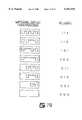
- FIG. 3Cillustrates encoding label configurations and corresponding identification codes provided by the label configurations according to the invention
- FIG. 4Ashows a ground strip of a printer cartridge identification circuit which is integral with a printhead TAB circuit according to the invention
- FIG. 4Billustrates an encoding label of a printhead identification circuit attached to a ground strip according to the invention
- FIG. 5is a schematic diagram of a printer cartridge identification circuit according to an alternative embodiment of the invention.
- FIG. 6Ashows the encoding circuit of a printer cartridge identification circuit which is nonintegral with a printhead TAB circuit according to the invention
- FIG. 6Bdepicts encoding circuit configurations and corresponding identification codes according to the invention.
- FIG. 7Adepicts an encoding circuit of a printer cartridge identification circuit which is nonintegral with a printhead TAB circuit according to the invention
- FIG. 7Bdepicts encoding circuit configurations and corresponding identification codes according to the invention.
- FIG. 8depicts the encoding circuit of a printer cartridge identification circuit which is nonintegral with a printhead TAB circuit according to the invention
- FIG. 9is a schematic diagram of a printer cartridge identification circuit using fusible links according to the invention.
- FIG. 10shows the identification pads and fusible links of a printer cartridge identification circuit which is integral with a printhead TAB circuit according to the invention
- FIG. 11is a schematic diagram of a printer cartridge identification circuit using trace breaches according to the invention.
- FIG. 12shows the identification pads and trace breaches of a printer cartridge identification circuit which is integral with a printhead TAB circuit according to the invention.
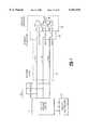
- FIG. 13is a schematic diagram of a preferred embodiment of a voltage sensing circuit according to the invention.
- a printer controller 10receives an electrical signal from a voltage sensing circuit 12 which senses voltage levels on each of three identification (ID) lines 15a, 15b, and 15c.
- a source voltage V LHis supplied to the ID lines 15a, 15b, and 15c through the bias resistors 14a, 14b, and 14c.
- the sensed voltage levels on the ID lines 15a, 15b, and 15care either V LH or ground (0 volts). For example, if the encoding switches 16a and 16c are closed with the encoding switch 16b open as shown in FIG.
- the voltage sensing circuit 12senses 0 volts on the ID lines 15a and 15c, and senses V LH on the ID line 15b.
- the voltage sensing circuit 12passes signals to the printer controller 10 which are indicative of the voltage levels sensed on the ID lines 15a, 15b, and 15c.
- the printer controller 10interprets the signals from the voltage sensing circuit 12 as identifying a particular type of printer cartridge installed in the printer.
- Two possible voltage levels (V LH or 0) on three ID linesprovide for eight (2 3 ) possible combinations. It should be appreciated that the number of possible combinations may be increased/decreased by a power of 2 by adding/removing a single ID line and encoding switch to/from the circuit of FIG. 1.
- the voltage levels on the ID lines 15a, 15b, and 15cwill be either V LH or ground potential depending on the states of the switches 16a, 16b, and 16c.
- the voltage level on the right side of the switches 16a, 16b, and 16ccould be any reference potential which can be differentiated from the source voltage V LH . Therefore, either V LH or a reference potential are sensed on the ID lines 15a, 15b, and 15c depending on the states of the switches 16a, 16b, and 16c.
- the reference potentialis ground potential.
- the reference potentialis referred to as ground potential in the description of the invention, the invention is not limited to sensing only ground as the reference potential on the ID lines 15a, 15b, and 15c.
- circuit shown in FIG. 1uses switches as the encoding means to establish or break the electrical path to ground for each of the ID lines 15, it should be appreciated that various other encoding means may be employed for this purpose. Regardless of the encoding means used, since the purpose of the encoding means is to encode identification information which is specific to each printer cartridge, it is desirable for the encoding means to be an integral part of the printer cartridge 18. This specification describes several embodiments of the invention which encode printer cartridge identification information utilizing various encoding means, wherein each embodiment provides a similar electrical function as the circuit represented in FIG. 1.
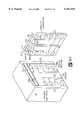
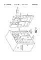
- FIG. 2 and the perspective views of FIGS. 3A and 3Billustrate a preferred embodiment of a printer cartridge identification circuit according to the invention.
- the printer connector 22includes a set of ID contacts 20a, 20b, and 20c which are arranged to make connection to a set of ID pads 24a, 24b, and 24c located on the printer cartridge 18.
- the ID pads 24a, 24b, and 24care discrete areas of highly conductive material such as gold and copper deposited on a flexible integrated circuit, such as a "TAB" circuit 27 (FIG. 3A).
- the TAB circuit 27typically includes many resistor circuit pads (shown generally at 25), and the printer connector 22 typically includes many resistor circuit pad contacts (shown generally at 23) to provide for electrical connection between the printer controller 10 and heating resistors in a printhead on the printer cartridge 18.
- FIG. 3Ashows only a few representative resistor circuit pads 25 and resistor circuit pad contacts 23.
- a TAB circuit ground 26is also shown in FIG. 3A.
- a ground potentialis supplied from the printer controller 10 to the TAB circuit ground 26 on the TAB circuit 27 through ground lines provided on the printer cable 19. To maintain the simplicity of FIG. 3A, these ground lines are not shown.
- the ID pads 24a, 24b, and 24care electrically connected to a TAB circuit ground 26 via traces 21a, 21b, and 21c.
- the ID pads 24a, 24b, and 24care arranged on the TAB circuit 27 to make electrical connection with the ID contacts 20a, 20b, and 20c on the printer connector 22 when the printer connector 22 is connected to the printer cartridge 18.
- ID lines 15a, 15b, and 15cwhich are part of a printer cable 19, have the ID contacts 20a, 20b, and 20c on one end thereof.
- the other ends of the ID lines 15a, 15b, and 15care connected to a voltage source V LH through bias resistors 14a, 14b, and 14c, and to a voltage sensing circuit 12 which senses the voltage levels on the ID lines 15a, 15b, and 15c. If an ID contact 20a, 20b, or 20c makes electrical connection with a corresponding ID pad 24a, 24b, or 24c, then the voltage sensing circuit 12 senses that the corresponding ID line 15a, 15b, or 15c is grounded.
- the voltage sensing circuit 12senses voltage V LH on the corresponding ID line 15a, 15b, or 15c.
- FIG. 3BA method for preventing or permitting one or more ID contacts 20a, 20b, and 20c from making electrical connection with the ID pads 24a, 24b, and 24c is shown in FIG. 3B.
- An encoding label 30, formed from electrically-nonconductive material such as paper or plasticis adhesively attached to the printer cartridge 18 adjacent to the ID pads 24a, 24b, and 24c.
- the label 30has either no aperture, or has one or more apertures, such as the holes 32a and 32c.
- the label 30selectively permits or prevents electrical connection between the ID contacts 20a, 20b, and 20c and the corresponding ID pads 24a, 24b, and 24c.
- ID pads 24a and 24cwhen the holes 32a and 32c coincide with the ID pads 24a and 24c, then the ID contacts 20a and 20c make electrical connection with the ID pads 24a and 24c when the printer connector 22 is connected to the printer cartridge 18.
- ID pad 24bsince there is no hole in the encoding label 30 over the ID pad 24b, the ID contact 20b is prevented from making electrical connection with the sense pad 24b.
- ID pad 24bis shown in outline form beneath the encoding label 30.
- the configuration of FIG. 3Bis depicted schematically in FIG. 2 which shows the ID contact 20b not touching the ID pad 24b.
- the voltage sensing circuit 12senses the ID lines 15a and 15c to be grounded, and senses V LH on the ID line 15b.
- the TAB circuit 27includes a single conductive ground strip 34 instead of individual ID pads as shown in FIGS. 3A and 3B.
- the function of the ground strip 34 and the ID contacts 20a, 20b, and 20cis similar to the function described with reference to FIGS. 3A and 3B.
- an encoding label 30covers a portion of the ground strip 34, thus preventing electrical connection between the ID contact 20b and the ground strip 34.
- Apertures 32a and 32cexpose selected areas of the ground strip 34, thus enabling electrical connection between the ID contacts 20a and 20c and the ground strip 34.
- the voltage sensing circuit 12(FIG. 1) senses the ID lines 15a and 15c to be grounded, and senses V LH on the ID line 15b.
- FIG. 3Cthere are eight possible configurations using the encoding label 30 with a printer connector 22 having three ID contacts 20a, 20b, and 20c.
- the eight corresponding identification codes listed in FIG. 3Cresult when using the voltage sensing circuit 12 shown in FIG. 13.
- FIG. 5 and FIG. 6AAn alternative printer cartridge identification circuit according to the invention is shown in FIG. 5 and FIG. 6A.
- an encoding circuit 38is provided separate from the TAB circuit 27. Because the encoding circuit 38 is separate from the TAB circuit 27, the encoding circuit 38 may be manufactured separately and attached to the printer cartridge 18 at the same or at a different point in the manufacturing process. Although the encoding circuit 38 and the TAB circuit 27 both reside on the printer cartridge 18, there is no permanent electrical connection on the printer cartridge 18 between the two circuits. However, as shown in FIG. 5, the two circuits may be electrically connected when the printer connector ground contact 36d contacts the encoding circuit 38, and the printer connector ground contact 36e, which is electrically connected to the ground contact 36d, contacts the TAB circuit ground pad 26a. Thus, the encoding circuit 38 is grounded to the TAB circuit 27 through the printer connector 22 when the printer connector 22 is attached to the printer cartridge 18.
- FIG. 6Adepicts one implementation of the circuit described with reference to FIG. 5.
- the encoding circuit 38consists of a single conductive strip, such as a strip of adhesive-backed copper or gold foil, which is attached to the printer cartridge 18 adjacent to the TAB circuit 27.
- the encoding circuit 38may also be formed from conductive materials such as copper and gold which have been deposited on the printer cartridge by means such as plating or vapor deposition.
- the encoding circuit 38makes electrical contact with some, all, or none of the ID contacts 36a, 36b, and 36c on the printer connector 22 depending on the configuration of the encoding circuit 38.
- the presence or absence of one or more holes in the encoding circuit 38 corresponding to ID contacts 36a, 36b, and 36cprovides the encoding scheme for the circuit 38.
- a hole 40bexists in the encoding circuit 38 at a location which corresponds with the connection point for the ID contact 36b. Due to the hole 40b, when the printer cartridge 18 is attached to the printer connector 22, the ID contact 36b does not make electrical connection with the encoding circuit 38. Since the printer cartridge 18 of this embodiment is constructed of electrically nonconductive material, there is no electrical continuity between the encoding circuit 38 and the ID contact 36b. However, the ID contacts 36a and 36c, which do make electrical contact with the encoding circuit 38, are electrically grounded.
- the voltage sensing circuit 12(FIG. 5) senses 0 volts on ID lines 15a and 15c, which are connected to ID contacts 36a and 36c respectively, and senses V LH on the ID line 15b which is connected to ID contact 36b.
- FIG. 6BThe configurations of the encoding circuit 38 using the contacts 36a, 36b, and 36c on the printer connector 22 are shown in FIG. 6B.
- the eight corresponding identification codes listed in FIG. 6Bresult when using the voltage sensing circuit 12 shown in FIG. 13.
- FIGS. 7A and 7Billustrate yet another aspect of the invention.
- an encoding circuit(indicated generally at 37) consists of selectively-placed encoding pads 39a and 39c and a ground pad 41 formed from electrically-conductive material, such as copper and gold, deposited on a nonconductive adhesive-backed film 40, such as Mylar tape.
- the encoding circuit 37is affixed to the printer cartridge 18 in a position which provides for electrical connection to the ID contacts 36a, 36b, and 36c on the printer connector 22.
- the encoding circuit ground pad 41makes electrical connection with the ground contact 36d when the printer connector 22 is attached to the printer cartridge 18.
- One or more of the ID contacts 36a, 36b, and 36care electrically grounded when one or more of the encoding pads 39a, 39b, and 39c on the encoding circuit 37 are present and are electrically connected to the ground pad 41 via a conductive trace 43. If none of the encoding pads 39a, 39b, and 39c are present, then none of the ID contacts are grounded.
- the encoding pads 39a and 39care positioned on the film 40 so as to make electrical contact with the ID contacts 36a and 36c when the printer connector 22 is attached to the printer cartridge 18. In the example of FIG. 7A, no encoding pad exists on the encoding circuit 37 at a location which coincides with the connection point of the ID contact 36b.
- the voltage sensing circuit 12senses 0 volts on the ID lines 15a and 15c which are connected to the ID contacts 36a and 36c respectively, and senses V LH on the ID line 15b which is connected to the ID contact 36b.
- FIG. 7BThe possible configurations of the encoding circuit 37 of this embodiment and the corresponding identification codes are shown in FIG. 7B.
- the eight corresponding identification codes listed in FIG. 7Bresult when using the voltage sensing circuit 12 shown in FIG. 13.
- the encoding circuit 38consists of a conductive strip, such as a strip of adhesive-backed copper or gold foil, which is attached to the printer cartridge 18 adjacent to, but separate from, the TAB circuit 27.
- the encoding circuit 38may also be formed from conductive materials such as copper and gold which have been deposited on the printer cartridge by means such as plating or vapor deposition.
- the encoding circuit 38makes electrical contact with some, all, or none of the ID contacts 36a, 36b, and 36c on the printer connector 22 depending on the configuration of an adhesive-backed nonconductive encoding label 42 which selectively covers portions of the encoding circuit 38. As shown in FIG.
- the encoding label 42 of this embodimentexposes a portion of the encoding circuit 38 which coincides with the connection point of the printer connector ground contact 36d.
- the encoding circuit 38is continuously grounded to the TAB circuit ground pad 26a when the printer connector 22 is attached to the printer cartridge 18.
- holes 44a, 44b, and 44c in the label 42 corresponding to the ID contacts 36a, 36b, and 36cprovides encoding for the circuit 38.
- holes 44a and 44cexist in the label 42 at locations which coincide with the connection points of ID contacts 36a and 36c, respectively. Due to the lack of a hole in the encoding label 42 at a location which corresponds to the connection point of the ID contact 36b, the ID contact 36b does not make electrical connection with the encoding circuit 38 when the printer cartridge 18 is attached to the printer connector 22.
- the voltage sensing circuit 12senses 0 volts on the ID lines 15a and 15c, which are connected to the ID contacts 36a and 36c respectively, and senses V LH on the ID line 15b which is connected to the ID contact 36b.
- the configurations of the encoding label 42 of this embodiment and the corresponding identification codesare similar to the configurations and codes shown in FIG. 3C. These identification codes result when using the voltage sensing circuit 12 shown in FIG. 13.
- FIGS. 9 and 10show still another embodiment of the features of the invention.
- ID pads 24a, 24b, and 24care electrically integral with a TAB circuit 27.
- ID contacts 20a, 20b, and 20care continuously electrically connected to the ID pads 24a, 24b, and 24c when the printer connector 22 is attached to the printer cartridge 18.
- Fusible traces 48a, 48b, and 48care used to electrically connect the ID pads 24a, 24b, and 24c to the TAB circuit ground 26.
- the traces 48a, 48b, and 48ccontain fusible links 46a, 46b, and 46c which can be selectively opened to break the connection between the ID pads 24a, 24b, and 24c and the TAB circuit ground 26.
- the fusible links 46a, 46b, and 46care sections of the traces 48a, 48b, and 48c which can be opened by passing an electrical current through them during or at the end of the cartridge manufacturing process.
- Printer cartridge identification informationis encoded by passing a high-current pulse through the trace or traces to be opened, and by not passing a high-current pulse through the trace or traces to remained closed.
- the high-current pulseopens the fusible link by melting or otherwise burning the link, thus creating an electrical discontinuity in the selected trace. For example, in FIG.
- the fusible link 46b in the trace 48bis open as indicated by the dotted line, such that no connection exists between the ID pad 24b and the TAB circuit ground 26.
- the voltage sensing circuit 12senses 0 volts on the ID lines 15a and 15c, which are connected to the ID contacts 20a and 20c respectively, and senses V LH on the ID line 15b which is connected to the ID contact 20b.
- the encoding circuitis similar to the circuit shown in FIGS. 9 and 10 with the exception that traces 50a, 50b, and 50c do not contain fusible links. Instead, the printer cartridge identification information is encoded during or at the end of the cartridge manufacturing process by creating a breach in selected traces by methods such as drilling, punching, abrading, or dissolving through portions of the selected traces. For example, in FIG. 12 the trace 50b is discontinuous, thereby electrically isolating the ID pad 24b from the TAB circuit ground 26.
- the voltage sensing circuit 12when the printer is in operation, the voltage sensing circuit 12 would sense 0 volts on the ID lines 15a and 15c, which are connected to the ID contacts 20a and 20c respectively, and would sense V LH on the ID line 15b which is connected to the ID contact 20b.
- a preferred voltage sensing circuit 12is shown in FIG. 13.
- the ID line 15a of the printer cable 19(FIG. 2) is connected to the base of a bipolar transistor 52a which acts as a switching device.
- Resistors 54a and 14aestablish the proper bias voltages on the collector and the base, respectively, of the transistor 52a.
- V LHwhich represents logic level one
- the transistor 52ais switched on, and 0 volts (logic level zero) exists on the collector of the transistor 52a.
- the ID line 15bis connected to the base of a bipolar transistor 52b.
- Resistors 54b and 14bestablish the proper bias voltages on the collector and the base, respectively, of the transistor 52b.
- V LHlogic level one
- the transistor 52bis off, and the source voltage V LH (logic level one), exists on the collector of the transistor 52b.
- V LHexists on the base of the transistor 52b thus switching the transistor 52b on.
- the transistor 52bis on, 0 volts (logic level zero) exists on its collector.
- the ID line 15cis connected to the base of a bipolar transistor 52c.
- the transistor 52cis off when the ID line 15c is grounded, in which case the source voltage V LH (logic level one) exists on the collector of the transistor 52c.
- V LHlogic level one
- V LHexists on the base of the transistor 52c.
- the transistor 52cis switched on, and 0 volts (logic level zero) exists on the collector of the transistor 52c.
- the voltage levels at the collectors of the transistors 52a, 52b, and 52care clocked into the latch circuits 56a, 56b, and 56c, respectively.
- the printer controller 10then reads the voltage levels on the latch circuits 56a, 56b, and 56c as a 3-bit code which identifies the type of printer cartridge 18 installed in the printer.
Landscapes
- Ink Jet (AREA)
Abstract
Description
The present invention is generally directed to ink jet printers, and is more particularly directed to an identification circuit attached to the printer cartridge of an ink jet printer for the encoding of cartridge-specific information.
Thermal ink jet printers apply ink to a print medium by ejecting small droplets of ink from an array of nozzles located in the printhead of a printer cartridge. An array of thin-film resistors on an integrated circuit on the printhead selectively generates heat as current is passed through the resistors. The generated heat causes ink contained within an ink reservoir to boil and be ejected from the array of nozzles that is adjacent to the resistor array. A printer controller determines which resistors will be "fired" and the proper firing sequence so that the desired pattern is printed on the medium.
Many multicolor ink jet printers accommodate replaceable ink cartridges containing multiple colors of ink as well as replaceable cartridges containing a single color of ink. The printer controllers of these printers require input of information identifying the type of cartridge that is installed so that the controllers are adjusted for proper printer operation with the installed cartridge. User interface is typically required to identify to the printer controller the type of cartridge installed.
In order to reduce the cost and complexity of printer cartridge manufacturing processes, it is desirable for all cartridges to be constructed with a similar configuration to the extent possible regardless of the type of cartridge or color of ink it contains. Thus it is desirable to maintain uniformity of cartridge configurations at least until the time that the cartridges are loaded with ink which typically occurs near the completion of the cartridge assembly process. However, maintaining a uniform cartridge configuration makes it difficult to easily identify the contents of the cartridge or the particular cartridge being used.
An object of the invention is to provide a relatively simple and inexpensive apparatus for encoding information on a printer cartridge.
Another object of the invention is to provide cartridge-specific information, such as ink color and type, on the cartridge in a manner that is detectable by the printer controller so that the controller is adjusted automatically without the need for user intervention.
A further object of the invention is to provide an encoding system which can be configured for a wide variety of printer cartridge types.
With regard to the above and other objects, the invention provides an apparatus which supplies information to a printer controller in order to identify the type of cartridge installed in an ink jet printer. The apparatus comprises a printer cable containing a set of electrically-conductive wires, each wire having a first end and a second end, with the first end of each of the wires being electrically connected to a voltage source. A printer connector has a set of electrically-conductive contacts which are connected to the second end of the printer cable wires, and which physically contact an identification circuit. The identification circuit, which is disposed upon the cartridge, contains an electrical conductor which is at an electrical reference potential. The identification circuit also includes a planar label which is attached to the cartridge. The label is composed of an electrically-nonconductive material having an adhesive material on one of its surfaces for adhesively attaching the label to the printer cartridge adjacent to the electrical conductor. The label covers and electrically insulates at least a portion of the electrical conductor to prevent the electrical conductor from making electrical connection with one or more of the printer connector contacts. The label has no apertures, or one or more apertures which expose one or more areas of the electrical conductor to electrical connection with one or more of the contacts. An input circuit is connected to the first ends of the printer cable wires for sensing which of the wires are at the reference potential. The input circuit also provides input signals to the printer controller corresponding to the wires which are at the reference potential.
According to the invention, the printer cartridge identification information is encoded by means of an adhesively-attached label. By encoding the identification information by means of an adhesively-attached label, the information can be easily incorporated into the printer cartridge at the end of the cartridge manufacturing process. Accordingly, only one cartridge design is required for a wide variety of inks and other services that the cartridge may perform.
In a preferred embodiment of the invention, the electrical conductor of the identification circuit includes one or more sense pads consisting of discrete areas of electrically-conductive material disposed upon a printer cartridge TAB circuit. Each of these sense pads are at a reference potential. A non-conductive encoding label having no apertures, or one or more apertures is adhesively applied to the cartridge in alignment with the sense pads on the TAB circuit. The label selectively permits or prevents connection between the sense pads and the connector contacts. In this manner, the printer cartridge identification information is encoded by the configuration of the apertures in the adhesively attached nonconductive label.
In another embodiment of the invention, the identification circuit includes an electrically-conductive planar strip which is at a reference potential. The strip has an adhesive material on one of its surfaces for adhesively attaching the strip to the printer cartridge. The identification circuit has no apertures, or one or more apertures in the strip which are positioned to coincide with one or more discrete connector contact points. The presence of one or more apertures preclude one or more of the connector contacts from making electrical connection to the strip. When there is no aperture, all of the connector contacts make electrical connection to the strip. In this manner, the printer cartridge identification information is encoded by the configuration of apertures in the adhesively-attached conductive strip.
In yet another embodiment of the invention, the electrical conductor of the identification circuit includes a planar label composed of electrically-nonconductive material. The label has an adhesive material on one of its surfaces for adhesively attaching the label to the printer cartridge. No sense pads, or one or more sense pads consisting of discrete areas of electrically-conductive material, are disposed upon the label. These sense pads, which are at a reference potential, are positioned on the label to coincide with one or more discrete connector contact points. Printer cartridge identification information is encoded by the number and position of the sense pads on the adhesively-attached label.
In another aspect, the invention provides an apparatus for providing thermal ink jet printer cartridge identification information to a printer controller to identify the cartridge installed in the printer, where the cartridge contains a printhead having an any of resistive heating elements. The apparatus includes a printer cable containing electrically-conductive wires, each having a first end and a second end. The apparatus also includes a printer connector having electrically-conductive contacts which are electrically connected to the second end of the printer cable wires, and which physically contact an identification circuit on the printer cartridge. The identification circuit, which is integral to a TAB circuit on the cartridge, contains an electrical conductor which is at an electrical reference potential relative to the array of resistive heating elements. The apparatus further includes means for precluding none, or one or more of the connector contacts from being at the reference potential relative to the array circuit of resistive heating elements, and means for enabling none, one or more of the contacts to be at the reference potential relative to the array circuit of resistive heating elements. An input circuit is connected to the first end of each of the printer cable wires for sensing which of the wires are at the reference potential relative to the electrical conductor on the printer cartridge, and for providing input signals to the printer controller corresponding to the wires which are at the reference potential.
Other aspects and advantages of the invention are provided by the following detailed description of preferred embodiments considered in conjunction with the following drawings, which are not to scale so as to better show the detail, in which like reference numerals denote like elements throughout the several views, and wherein:
FIGS. 1 and 2 are schematic diagrams of printer cartridge identification circuits according to the invention;
FIG. 3A illustrates identification pads of a printer cartridge identification circuit which are integral with a printhead TAB circuit according to one aspect of the invention;
FIG. 3B depicts an encoding label of a printhead identification circuit according to another aspect of the invention;
FIG. 3C illustrates encoding label configurations and corresponding identification codes provided by the label configurations according to the invention;
FIG. 4A shows a ground strip of a printer cartridge identification circuit which is integral with a printhead TAB circuit according to the invention;
FIG. 4B illustrates an encoding label of a printhead identification circuit attached to a ground strip according to the invention;
FIG. 5 is a schematic diagram of a printer cartridge identification circuit according to an alternative embodiment of the invention;
FIG. 6A shows the encoding circuit of a printer cartridge identification circuit which is nonintegral with a printhead TAB circuit according to the invention;
FIG. 6B depicts encoding circuit configurations and corresponding identification codes according to the invention;
FIG. 7A depicts an encoding circuit of a printer cartridge identification circuit which is nonintegral with a printhead TAB circuit according to the invention;
FIG. 7B depicts encoding circuit configurations and corresponding identification codes according to the invention;
FIG. 8 depicts the encoding circuit of a printer cartridge identification circuit which is nonintegral with a printhead TAB circuit according to the invention;
FIG. 9 is a schematic diagram of a printer cartridge identification circuit using fusible links according to the invention;
FIG. 10 shows the identification pads and fusible links of a printer cartridge identification circuit which is integral with a printhead TAB circuit according to the invention;
FIG. 11 is a schematic diagram of a printer cartridge identification circuit using trace breaches according to the invention;
FIG. 12 shows the identification pads and trace breaches of a printer cartridge identification circuit which is integral with a printhead TAB circuit according to the invention; and
FIG. 13 is a schematic diagram of a preferred embodiment of a voltage sensing circuit according to the invention.
The overall concept of the printer cartridge identification circuit according to the invention is illustrated in FIG. 1. As shown in FIG. 1, aprinter controller 10 receives an electrical signal from avoltage sensing circuit 12 which senses voltage levels on each of three identification (ID)lines ID lines encoding switches printer cartridge 18, the sensed voltage levels on theID lines encoding switch 16b open as shown in FIG. 1, then thevoltage sensing circuit 12 senses 0 volts on theID lines ID line 15b. Thevoltage sensing circuit 12 passes signals to theprinter controller 10 which are indicative of the voltage levels sensed on theID lines printer controller 10 interprets the signals from thevoltage sensing circuit 12 as identifying a particular type of printer cartridge installed in the printer. Two possible voltage levels (VLH or 0) on three ID lines provide for eight (23) possible combinations. It should be appreciated that the number of possible combinations may be increased/decreased by a power of 2 by adding/removing a single ID line and encoding switch to/from the circuit of FIG. 1.
In the preferred embodiment of the invention, the voltage levels on theID lines switches switches ID lines switches ID lines
Although the circuit shown in FIG. 1 uses switches as the encoding means to establish or break the electrical path to ground for each of the ID lines 15, it should be appreciated that various other encoding means may be employed for this purpose. Regardless of the encoding means used, since the purpose of the encoding means is to encode identification information which is specific to each printer cartridge, it is desirable for the encoding means to be an integral part of theprinter cartridge 18. This specification describes several embodiments of the invention which encode printer cartridge identification information utilizing various encoding means, wherein each embodiment provides a similar electrical function as the circuit represented in FIG. 1.
The schematic of FIG. 2 and the perspective views of FIGS. 3A and 3B illustrate a preferred embodiment of a printer cartridge identification circuit according to the invention. When areplaceable printer cartridge 18 is installed in a thermal ink jet printer, theprinter cartridge 18 is in electrical contact with aprinter connector 22. Theprinter connector 22 includes a set ofID contacts ID pads printer cartridge 18. Preferably, theID pads TAB circuit 27 typically includes many resistor circuit pads (shown generally at 25), and theprinter connector 22 typically includes many resistor circuit pad contacts (shown generally at 23) to provide for electrical connection between theprinter controller 10 and heating resistors in a printhead on theprinter cartridge 18. However, in the interest of clarity, FIG. 3A shows only a few representativeresistor circuit pads 25 and resistorcircuit pad contacts 23. ATAB circuit ground 26 is also shown in FIG. 3A. A ground potential is supplied from theprinter controller 10 to theTAB circuit ground 26 on theTAB circuit 27 through ground lines provided on theprinter cable 19. To maintain the simplicity of FIG. 3A, these ground lines are not shown. TheID pads TAB circuit ground 26 viatraces 21a, 21b, and 21c. TheID pads TAB circuit 27 to make electrical connection with theID contacts printer connector 22 when theprinter connector 22 is connected to theprinter cartridge 18.
As shown in FIG. 2,ID lines printer cable 19, have theID contacts ID lines voltage sensing circuit 12 which senses the voltage levels on theID lines ID contact corresponding ID pad voltage sensing circuit 12 senses that thecorresponding ID line ID contact corresponding ID pad voltage sensing circuit 12 senses voltage VLH on thecorresponding ID line
A method for preventing or permitting one ormore ID contacts ID pads encoding label 30, formed from electrically-nonconductive material such as paper or plastic is adhesively attached to theprinter cartridge 18 adjacent to theID pads label 30 has either no aperture, or has one or more apertures, such as theholes label 30 selectively permits or prevents electrical connection between theID contacts corresponding ID pads holes ID pads ID contacts ID pads printer connector 22 is connected to theprinter cartridge 18. However, since there is no hole in theencoding label 30 over theID pad 24b, theID contact 20b is prevented from making electrical connection with thesense pad 24b.ID pad 24b is shown in outline form beneath theencoding label 30. The configuration of FIG. 3B is depicted schematically in FIG. 2 which shows theID contact 20b not touching theID pad 24b. If thelabel 30 contains theholes printer connector 22 attached to theprinter cartridge 18, then thevoltage sensing circuit 12 senses theID lines ID line 15b.
There are eight possible hole placement configurations using theencoding label 30 over theID pads voltage sensing circuit 12 shown in FIG. 13.
An alternative aspect of the invention is shown in FIG. 4A. In this embodiment, theTAB circuit 27 includes a singleconductive ground strip 34 instead of individual ID pads as shown in FIGS. 3A and 3B. Although this arrangement provides a different physical configuration compared to the embodiment of FIG. 3A, the function of theground strip 34 and theID contacts encoding label 30 covers a portion of theground strip 34, thus preventing electrical connection between theID contact 20b and theground strip 34.Apertures ground strip 34, thus enabling electrical connection between theID contacts ground strip 34. In the configuration shown in FIG. 4B, with theprinter connector 22 attached to theprinter cartridge 18 and the printer in operation, the voltage sensing circuit 12 (FIG. 1) senses theID lines ID line 15b.
As shown in FIG. 3C, there are eight possible configurations using theencoding label 30 with aprinter connector 22 having threeID contacts voltage sensing circuit 12 shown in FIG. 13.
An alternative printer cartridge identification circuit according to the invention is shown in FIG. 5 and FIG. 6A. In this embodiment, anencoding circuit 38 is provided separate from theTAB circuit 27. Because theencoding circuit 38 is separate from theTAB circuit 27, theencoding circuit 38 may be manufactured separately and attached to theprinter cartridge 18 at the same or at a different point in the manufacturing process. Although theencoding circuit 38 and theTAB circuit 27 both reside on theprinter cartridge 18, there is no permanent electrical connection on theprinter cartridge 18 between the two circuits. However, as shown in FIG. 5, the two circuits may be electrically connected when the printerconnector ground contact 36d contacts theencoding circuit 38, and the printerconnector ground contact 36e, which is electrically connected to theground contact 36d, contacts the TABcircuit ground pad 26a. Thus, theencoding circuit 38 is grounded to theTAB circuit 27 through theprinter connector 22 when theprinter connector 22 is attached to theprinter cartridge 18.
FIG. 6A depicts one implementation of the circuit described with reference to FIG. 5. In this embodiment, theencoding circuit 38 consists of a single conductive strip, such as a strip of adhesive-backed copper or gold foil, which is attached to theprinter cartridge 18 adjacent to theTAB circuit 27. Theencoding circuit 38 may also be formed from conductive materials such as copper and gold which have been deposited on the printer cartridge by means such as plating or vapor deposition. When theprinter cartridge 18 is attached to theprinter connector 22, theencoding circuit 38 makes electrical contact with some, all, or none of theID contacts printer connector 22 depending on the configuration of theencoding circuit 38. The presence or absence of one or more holes in theencoding circuit 38 corresponding toID contacts circuit 38. For example, in the configuration shown in FIG. 6A, ahole 40b exists in theencoding circuit 38 at a location which corresponds with the connection point for theID contact 36b. Due to thehole 40b, when theprinter cartridge 18 is attached to theprinter connector 22, theID contact 36b does not make electrical connection with theencoding circuit 38. Since theprinter cartridge 18 of this embodiment is constructed of electrically nonconductive material, there is no electrical continuity between theencoding circuit 38 and theID contact 36b. However, theID contacts encoding circuit 38, are electrically grounded. Thus, the voltage sensing circuit 12 (FIG. 5) senses 0 volts onID lines ID contacts ID line 15b which is connected toID contact 36b.
The configurations of theencoding circuit 38 using thecontacts printer connector 22 are shown in FIG. 6B. The eight corresponding identification codes listed in FIG. 6B result when using thevoltage sensing circuit 12 shown in FIG. 13.
FIGS. 7A and 7B illustrate yet another aspect of the invention. As shown in FIG. 7A, an encoding circuit (indicated generally at 37) consists of selectively-placed encoding pads 39a and 39c and a ground pad 41 formed from electrically-conductive material, such as copper and gold, deposited on a nonconductive adhesive-backedfilm 40, such as Mylar tape. Theencoding circuit 37 is affixed to theprinter cartridge 18 in a position which provides for electrical connection to theID contacts printer connector 22. The encoding circuit ground pad 41 makes electrical connection with theground contact 36d when theprinter connector 22 is attached to theprinter cartridge 18. One or more of theID contacts encoding circuit 37 are present and are electrically connected to the ground pad 41 via aconductive trace 43. If none of the encoding pads 39a, 39b, and 39c are present, then none of the ID contacts are grounded. For example, as shown in FIG. 7A, the encoding pads 39a and 39c are positioned on thefilm 40 so as to make electrical contact with theID contacts printer connector 22 is attached to theprinter cartridge 18. In the example of FIG. 7A, no encoding pad exists on theencoding circuit 37 at a location which coincides with the connection point of theID contact 36b. In this configuration, since thefilm 40 is formed from electrically nonconductive material, there is no electrical continuity between the ground pad 41 and theID contact 36b. Therefore, when theprinter connector 22 is attached to theprinter cartridge 18, and the printer is in operation, thevoltage sensing circuit 12 senses 0 volts on theID lines ID contacts ID line 15b which is connected to theID contact 36b.
The possible configurations of theencoding circuit 37 of this embodiment and the corresponding identification codes are shown in FIG. 7B. The eight corresponding identification codes listed in FIG. 7B result when using thevoltage sensing circuit 12 shown in FIG. 13.
Another embodiment of the invention is shown in FIG. 8. In this embodiment, theencoding circuit 38 consists of a conductive strip, such as a strip of adhesive-backed copper or gold foil, which is attached to theprinter cartridge 18 adjacent to, but separate from, theTAB circuit 27. Theencoding circuit 38 may also be formed from conductive materials such as copper and gold which have been deposited on the printer cartridge by means such as plating or vapor deposition. When theprinter cartridge 18 is attached to theprinter connector 22, theencoding circuit 38 makes electrical contact with some, all, or none of theID contacts printer connector 22 depending on the configuration of an adhesive-backednonconductive encoding label 42 which selectively covers portions of theencoding circuit 38. As shown in FIG. 8, theencoding label 42 of this embodiment exposes a portion of theencoding circuit 38 which coincides with the connection point of the printerconnector ground contact 36d. Thus, theencoding circuit 38 is continuously grounded to the TABcircuit ground pad 26a when theprinter connector 22 is attached to theprinter cartridge 18.
The presence or absence of one or more holes 44a, 44b, and 44c in thelabel 42 corresponding to theID contacts circuit 38. For example, as shown in FIG. 8, holes 44a and 44c exist in thelabel 42 at locations which coincide with the connection points ofID contacts encoding label 42 at a location which corresponds to the connection point of theID contact 36b, theID contact 36b does not make electrical connection with theencoding circuit 38 when theprinter cartridge 18 is attached to theprinter connector 22. In this configuration, when the printer is operating, thevoltage sensing circuit 12 senses 0 volts on theID lines ID contacts ID line 15b which is connected to theID contact 36b.
The configurations of theencoding label 42 of this embodiment and the corresponding identification codes are similar to the configurations and codes shown in FIG. 3C. These identification codes result when using thevoltage sensing circuit 12 shown in FIG. 13.
FIGS. 9 and 10 show still another embodiment of the features of the invention. In this embodiment,ID pads TAB circuit 27. However, as shown in FIGS. 9 and 10,ID contacts ID pads printer connector 22 is attached to theprinter cartridge 18. Fusible traces 48a, 48b, and 48c are used to electrically connect theID pads TAB circuit ground 26. Thetraces fusible links ID pads TAB circuit ground 26. Thefusible links traces fusible link 46b in thetrace 48b is open as indicated by the dotted line, such that no connection exists between theID pad 24b and theTAB circuit ground 26. In this configuration, when the printer is in operation and theprinter connector 22 is connected to theprinter cartridge 18, thevoltage sensing circuit 12 senses 0 volts on theID lines ID contacts ID line 15b which is connected to theID contact 20b.
In FIGS. 11 and 12, the encoding circuit is similar to the circuit shown in FIGS. 9 and 10 with the exception that traces 50a, 50b, and 50c do not contain fusible links. Instead, the printer cartridge identification information is encoded during or at the end of the cartridge manufacturing process by creating a breach in selected traces by methods such as drilling, punching, abrading, or dissolving through portions of the selected traces. For example, in FIG. 12 thetrace 50b is discontinuous, thereby electrically isolating theID pad 24b from theTAB circuit ground 26. In this configuration, when the printer is in operation, thevoltage sensing circuit 12 would sense 0 volts on theID lines ID contacts ID line 15b which is connected to theID contact 20b.
A preferredvoltage sensing circuit 12 is shown in FIG. 13. TheID line 15a of the printer cable 19 (FIG. 2) is connected to the base of abipolar transistor 52a which acts as a switching device. Resistors 54a and 14a establish the proper bias voltages on the collector and the base, respectively, of thetransistor 52a. When theID line 15a is grounded, thetransistor 52a is off, and the source voltage VLH, which represents logic level one, exists on the collector oftransistor 52a. When theID line 15a is not grounded, VLH exists on the base of thetransistor 52a. In this situation, thetransistor 52a is switched on, and 0 volts (logic level zero) exists on the collector of thetransistor 52a.
Similarly, theID line 15b is connected to the base of abipolar transistor 52b. Resistors 54b and 14b establish the proper bias voltages on the collector and the base, respectively, of thetransistor 52b. When theID line 15b is grounded, thetransistor 52b is off, and the source voltage VLH (logic level one), exists on the collector of thetransistor 52b. When theID line 15b is not grounded, VLH exists on the base of thetransistor 52b thus switching thetransistor 52b on. When thetransistor 52b is on, 0 volts (logic level zero) exists on its collector.
In a like manner, theID line 15c is connected to the base of abipolar transistor 52c. Thetransistor 52c is off when theID line 15c is grounded, in which case the source voltage VLH (logic level one) exists on the collector of thetransistor 52c. However, when theID line 15c is not grounded, VLH exists on the base of thetransistor 52c. In this situation, thetransistor 52c is switched on, and 0 volts (logic level zero) exists on the collector of thetransistor 52c.
The voltage levels at the collectors of thetransistors latch circuits printer controller 10 then reads the voltage levels on thelatch circuits printer cartridge 18 installed in the printer.
It is contemplated, and will be apparent to those skilled in the art from the preceding description and the accompanying drawings that modifications and additions may be made in the embodiments of the invention. For example, while the preferred embodiments implement a three-bit code to identify printer cartridge characteristics, the scope of the invention is not limited to an apparatus for encoding any particular number of bits. Furthermore, the scope of the invention is not limited to the identification of printer cartridges only, but is also applicable to the identification of any type of interchangeable or replaceable accessory cartridge which may be installed in an ink jet printer. For example, the invention is also applicable to the identification of a scanning device cartridge which is installed in place of, or in addition to, a printer cartridge. Accordingly, it is expressly intended that the foregoing description and the accompanying drawings are illustrative of preferred embodiments only, not limiting thereto, and that the spirit and scope of the invention be determined by reference to the following claims.
Claims (25)
1. An apparatus for providing identification information to a printer controller of a thermal inkjet printer, the information relating to a thermal ink jet printer cartridge, the apparatus comprising:
a printer cable comprising electrically-conductive wires, each wire having a first end and a second end, the first end of each ofthe wires being electrically connected to a voltage source;
a printer connector having electrically-conductive contacts electrically connected to the second end of the wires, the contacts physically contacting an identification circuit;
the identification circuit disposed upon the printer cartridge, the identification circuit either integral to or separate from a TAB circuit on the cartridge, the identification circuit comprising:
an electrical conductor which is at a reference potential; and
a planar label composed of electrically-nonconductive material having an adhesive material on one surface thereof for adhesively attaching the label to the printer cartridge adjacent the electrical conductor to cover and electrically insulate at least a portion of the electrical conductor, the label having no apertures, or one or more apertures which expose one or more areas of the electrical conductor to electrical connection with one or more of the contacts; and
an input circuit connected to the first end of each of the wires for sensing which of the wires are at the reference potential, and for providing input signals to the printer controller corresponding to the wires which are at the reference potential.
2. The apparatus of claim 1 wherein the reference potential is ground potential.
3. The apparatus of claim 2 wherein the electrical conductor further comprises one or more sense pads consisting of discrete areas of electrically-conductive material disposed upon the printer cartridge.
4. The apparatus of claim 1 wherein the electrical conductor further comprises one or more sense pads consisting of discrete areas of electrically-conductive material disposed upon the printer cartridge.
5. The apparatus of claim 3 wherein the electrical conductor further comprises:
at least one circuit ground consisting of a discrete area of electrically-conductive material disposed upon the printer cartridge TAB circuit; and
traces between the sense pads and the circuit ground, each trace consisting of a discrete area of electrically-conductive material disposed upon the printer cartridge TAB circuit between the sense pads and the circuit ground.
6. The apparatus of claim 1 wherein the input circuit further comprises:
switching devices having at least a first port and a second port, the second port of each switching device being electrically connected to the first end of a corresponding one of the wires, the first port of each switching device assuming a first logic voltage level when the corresponding one of the wires is at an electrical reference potential, and the first port of each switching device assuming a second logic voltage level when the corresponding one of the wires is not at the electrical reference potential; and
holding devices having at least an input port and an output port, the input port of each of the holding devices being electrically connected to a first port of a corresponding one of the switching devices, the output port of each of the holding devices being electrically connected to the printer controller, each of the holding devices transferring a logic voltage level at the input port of the holding device to the printer controller.
7. An apparatus for providing identification information to a printer controller of a thermal ink jet printer, the information relating to a thermal ink jet printer cartridge, the cartridge containing a printhead disposed thereon, the printhead having an array circuit of resistive heating elements, the apparatus comprising:
a printer cable comprising electrically-conductive wires, each wire having a first end and a second end;
a printer connector having electrically-conductive contacts electrically connected to the second end of the wires, the contacts physically contacting an identification circuit;
the identification circuit disposed upon the printer cartridge, the identification circuit being integral to a TAB circuit on the cartridge, the identification circuit comprising:
an electrical conductor which is at an electrical reference potential relative to the array circuit of resistive heating elements;
means for precluding none, or one or more of the contacts from being at the reference potential relative to the array circuit of resistive heating elements, the means comprising a planar label composed of electrically-nonconductive material having an adhesive material on one surface thereof for adhesively attaching the label to the printer cartridge adjacent the electrical conductor to cover and electrically insulate at least a portion of the electrical conductor from making electrical connection with the contacts; and
means for enabling none, or one or more of the contacts to be at the reference potential relative to the array circuit of resistive heating elements; and
an input circuit connected to the first end of each of the wires for sensing which of the wires are at the reference potential relative to the array circuit of resistive heating elements, and for providing input signals to the printer controller corresponding to the wires which are at the reference potential.
8. The apparatus of claim 7 wherein the reference potential is ground potential.
9. The apparatus of claim 7 wherein the means for enabling none, or one or more of the contacts to be at the reference potential relative to the array circuit of resistive heating elements comprise no aperture, or one or more apertures disposed in the label to expose none of, or one or more portions of the electrical conductor for electrical connection with the contacts.
10. The apparatus of claim 7 wherein the input circuit further comprises:
switching devices having at least a first port and a second port, the second port of each switching device being electrically connected to the first end of a corresponding one of the wires, the first port of each switching device assuming a first logic voltage level when the corresponding one of the wires is at the reference potential relative to the array circuit of resistive heating elements, and the first port of each switching device assuming a second logic voltage level when the corresponding one of the wires is not at the reference potential relative to the array circuit of resistive heating elements; and
holding devices having at least an input port and an output port, the input port of each of the holding devices being electrically connected to a first port of a corresponding one of the switching devices, the output port of each of the holding devices being electrically connected to the printer controller, each of the holding devices transferring a logic voltage level at the input port of the holding device to the printer controller.
11. The apparatus of claim 7 wherein the electrical conductor further comprises:
sense pads, each sense pad consisting of a discrete area of electrically-conductive material disposed upon the printer cartridge;
a circuit ground which is electrically grounded relative to the array circuit of resistive heating elements; and
traces between the sense pads and the circuit ground, each trace consisting of a discrete area of electrically-conductive material disposed upon the printer cartridge between the sense pads and the circuit ground.
12. The apparatus of claim 11 wherein the planar label is attached to the printer cartridge adjacent the sense pads to cover and electrically insulate none, or one or more of the sense pads from contact with the one or more contacts.
13. The apparatus of claim 12 wherein the means for enabling none, or one or more of the contacts to be at the reference potential relative to the array circuit of resistive heating elements comprise no aperture, or one or more apertures disposed in the label to expose none, or one or more of the sense pads to electrical connection with the one or more contacts.
14. An apparatus for use with a thermal ink jet printer which is capable of accommodating different types of accessory cartridges, the apparatus providing information to an accessory controller to identify the type of accessory cartridge installed in the ink jet printer, the apparatus comprising:
a printer cable comprising electrically-conductive wires, each wire having a first end and a second end, the first end of each of the wires being electrically connected to a voltage source;
a printer connector having electrically-conductive contacts electrically connected to the second end of the wires, the contacts physically contacting an identification circuit;
the identification circuit disposed upon the accessory cartridge, the identification circuit comprising:
an electrical conductor which is at a reference potential;
a planar label composed of electrically-nonconductive material having an adhesive material on one surface thereof for adhesively attaching the label to the accessory cartridge adjacent the electrical conductor to cover and electrically insulate at least a portion of the electrical conductor, the label having no apertures, or one or more apertures which expose one or more areas of the electrical conductor to electrical connection with one or more of the contacts; and
an input circuit connected to the first end of each of the wires for sensing which of the wires are at the reference potential, and for providing input signals to the accessory controller corresponding to the wires which are at the reference potential.
15. The apparatus of claim 14 wherein the reference potential is ground potential.
16. The apparatus of claim 14 wherein the electrical conductor further comprises one or more sense pads consisting of discrete areas of electrically-conductive material disposed upon the accessory cartridge.
17. The apparatus of claim 16 wherein the electrical conductor further comprises:
at least one circuit ground consisting of a discrete area of electrically-conductive material disposed upon the accessory cartridge; and
traces between the sense pads and the circuit ground, each trace consisting of a discrete area of electrically-conductive material disposed upon the accessory cartridge between the sense pads and the circuit ground.
18. The apparatus of claim 14 wherein the input circuit further comprises:
switching devices having at least a first port and a second port, the second port of each switching device being electrically connected to the first end of a corresponding one of the wires, the first port of each switching device assuming a first logic voltage level when the corresponding one of the wires is at an electrical reference potential, and the first port of each switching device assuming a second logic voltage level when the corresponding one of the wires is not at the electrical reference potential; and
holding devices having at least an input port and an output port, the input port of each of the holding devices being electrically connected to a first port of a corresponding one of the switching devices, the output port of each of the holding devices being electrically connected to the accessory controller, each of the holding devices transferring a logic voltage level at the input port of the holding device to the accessory controller.
19. An apparatus for use with a thermal ink jet printer which is capable of accommodating different types of accessory cartridges, the apparatus providing information to an accessory controller to identify the type of accessory cartridge installed in the ink jet printer, the apparatus comprising:
a printer cable comprising electrically-conductive wires, each wire having a first end and a second end;
a printer connector having electrically-conductive contacts electrically connected to the second end of the wires, the contacts physically contacting an identification circuit;
the identification circuit disposed upon the accessory cartridge, the circuit comprising:
an electrical conductor which is at an electrical reference potential;
means for precluding none, or one or more of the contacts from being at the reference potential, the means comprising a planar label composed of electrically-nonconductive material having an adhesive material on one surface thereof for adhesively attaching the label to the accessory cartridge adjacent the electrical conductor to cover and electrically insulate at least a portion of the electrical conductor from making electrical connection with the contacts; and
means for enabling none, or one or more contacts to be at the reference potential; and
an input circuit connected to the first end of each of the wires for sensing which of the wires are at the reference potential, and for providing input signals to the accessory controller corresponding to the wires which are at the reference potential.
20. The apparatus of claim 19 wherein the reference potential is ground potential.
21. The apparatus of claim 19 wherein the means for enabling none, or one or more of the contacts to be at the reference potential comprise no aperture, or one or more apertures disposed in the label to expose none, or one or more portions of the electrical conductor for electrical connection with the contacts.
22. The apparatus of claim 19 wherein the input circuit further comprises:
switching devices having at least a first port and a second port, the second port of each switching device being electrically connected to the first end of a corresponding one of the wires, the first port of each switching device assuming a first logic voltage level when the corresponding one of the wires is at the reference potential, and the first port of each switching device assuming a second logic voltage level when the corresponding one of the wires is not at the reference potential; and
holding devices having at least an input port and an output port, the input port of each of the holding devices being electrically connected to a first port of a corresponding one of the switching devices, the output port of each of the holding devices being electrically connected to the accessory controller, each of the holding devices transferring a logic voltage level at the input port of the holding device to the accessory controller.
23. The apparatus of claim 19 wherein the electrical conductor further comprises:
sense pads, each sense pad consisting of a discrete area of electrically-conductive material disposed upon the accessory cartridge;
a circuit ground which is at an electrical reference potential; and
traces between the sense pads and the circuit ground, each trace consisting of a discrete area of electrically-conductive material disposed upon the accessory cartridge between the sense pads and the circuit ground.
24. The apparatus of claim 23 wherein the planar label is attached to the accessory cartridge adjacent the sense pads to cover and electrically insulate none, or one or more of the sense pads from contact with the one or more contacts.
25. The apparatus of claim 24 wherein the means for enabling none, or one or more of the contacts to be at the reference potential comprise no aperture, or one or more apertures disposed in the label to expose none, or one or more of the sense pads to electrical connection with the one or more contacts.
Priority Applications (1)
| Application Number | Priority Date | Filing Date | Title |
|---|---|---|---|
| US09/099,814US6161915A (en) | 1998-06-19 | 1998-06-19 | Identification of thermal inkjet printer cartridges |
Applications Claiming Priority (1)
| Application Number | Priority Date | Filing Date | Title |
|---|---|---|---|
| US09/099,814US6161915A (en) | 1998-06-19 | 1998-06-19 | Identification of thermal inkjet printer cartridges |
Publications (1)
| Publication Number | Publication Date |
|---|---|
| US6161915Atrue US6161915A (en) | 2000-12-19 |
Family
ID=22276752
Family Applications (1)
| Application Number | Title | Priority Date | Filing Date |
|---|---|---|---|
| US09/099,814Expired - LifetimeUS6161915A (en) | 1998-06-19 | 1998-06-19 | Identification of thermal inkjet printer cartridges |
Country Status (1)
| Country | Link |
|---|---|
| US (1) | US6161915A (en) |
Cited By (69)
| Publication number | Priority date | Publication date | Assignee | Title |
|---|---|---|---|---|
| US6260942B1 (en)* | 1999-10-22 | 2001-07-17 | Lexmark International, Inc. | Sensor and method for detecting protective tape on a printer cartridge |
| US20010035964A1 (en)* | 2000-04-20 | 2001-11-01 | Hiroyasu Kurashina | Tape cartridge, tape printing method, tape printing apparatus, and label-producing method |
| US6360174B1 (en)* | 1998-05-08 | 2002-03-19 | Funai Electric Co., Ltd. | Apparatus for detecting quantity level of residual ink in ink cartridge |
| US6390585B1 (en)* | 1998-07-21 | 2002-05-21 | Hewlett-Packard Company | Selectively warming a printhead for optimized performance |
| US6416154B1 (en)* | 1997-07-12 | 2002-07-09 | Silverbrook Research Pty Ltd | Printing cartridge with two dimensional code identification |
| EP1219437A3 (en)* | 2000-12-26 | 2002-11-06 | Seiko Epson Corporation | Terminals for circuit board |
| US6533396B2 (en)* | 2001-08-16 | 2003-03-18 | Benq Corporation | Printhead cartridge with asymmetrical contacts |
| US20030058304A1 (en)* | 2001-09-25 | 2003-03-27 | Chih-Ching Chen | Inkjet apparatus and method of preventing misplacing inkjet cartridge therein |
| US20030058625A1 (en)* | 2001-09-25 | 2003-03-27 | Chih-Ching Chen | Identifiable flexible printed circuit board and method of fabricating the same |
| US6547364B2 (en) | 1997-07-12 | 2003-04-15 | Silverbrook Research Pty Ltd | Printing cartridge with an integrated circuit device |
| US6644771B1 (en) | 1997-07-12 | 2003-11-11 | Silverbrook Research Pty Ltd | Printing cartridge with radio frequency identification |
| US6644876B2 (en) | 2001-11-01 | 2003-11-11 | Brady Worldwide, Inc. | Method and apparatus for printer cartridge identification |
| US6672699B1 (en)* | 1999-09-13 | 2004-01-06 | Samsung Electronics Co., Ltd. | Apparatus for determining cartridge type of printer using micro injecting device |
| US6736487B2 (en)* | 2002-09-26 | 2004-05-18 | Static Control Components, Inc. | Printer cartridge and method of making or refurbishing |
| US20040102868A1 (en)* | 2002-11-21 | 2004-05-27 | Thomas Linehan | Connection error detection and response |
| US20040125397A1 (en)* | 2002-12-30 | 2004-07-01 | Adkins Christopher Alan | Licensing method for use with an imaging device |
| US20040138945A1 (en)* | 2003-01-15 | 2004-07-15 | Adkins Christopher Alan | Method for reducing the cost of imaging for customers |
| US6767147B2 (en) | 2002-06-14 | 2004-07-27 | Amano Cincinnati, Inc. | Coded ribbon cartridge, decoder, and ribbon ink capacity indicator with LCD display |
| US20040165041A1 (en)* | 2002-08-01 | 2004-08-26 | Chih-Ching Chen | Identifiable inkjet cartridge and method of preventing misplacing inkjet cartridge in an inkjet apparatus |
| DE10244195B4 (en)* | 2001-09-25 | 2004-09-09 | Benq Corp. | Ink cartridge and flexible color circuit board |
| US20040212652A1 (en)* | 1997-07-12 | 2004-10-28 | Kia Silverbrook | Printing cartridge with pressure sensor array identification |
| US20040212651A1 (en)* | 2003-04-25 | 2004-10-28 | Johnson Bruce L. | Replaceable printer component |
| US6811240B2 (en) | 2002-04-30 | 2004-11-02 | Industrial Technology Research Institute | Manufacturing method for an ID circuit of inkjet chips |
| US20040218934A1 (en)* | 2001-08-06 | 2004-11-04 | Kia Silverbrook | Printing cartridge with barcode identification |
| US20040218023A1 (en)* | 2003-04-29 | 2004-11-04 | Hewlett- Packard Development Company, L.P. | Cartridge tape removal apparatus and method |
| US6830391B2 (en)* | 2001-09-21 | 2004-12-14 | Panduit Corp. | Media cartridge with printed circuit board for use in a printing system |
| US20050093943A1 (en)* | 2003-10-31 | 2005-05-05 | O'hara Steve | Interconnect circuit |
| US20050093909A1 (en)* | 2001-10-22 | 2005-05-05 | Kia Silverbrook | Printing cartridge with switch array identification |
| US20050157128A1 (en)* | 2004-01-21 | 2005-07-21 | Silverbrook Research Pty Ltd | Pagewidth inkjet printer cartridge with end electrical connectors |
| US20050162455A1 (en)* | 2001-08-06 | 2005-07-28 | Kia Silverbrook | Printing cartridge with an integrated circuit device |
| US20050174370A1 (en)* | 2004-02-06 | 2005-08-11 | Sarmast Sam M. | Fluid ejection device identification |
| AU2005200088B2 (en)* | 2001-08-06 | 2005-10-27 | Zamtec Limited | Printing control based on two dimensional code indicative of printing cartridge |
| US20050259123A1 (en)* | 2004-02-13 | 2005-11-24 | Hugh Rice | Device identification using a programmable memory circuit |
| US20060017756A1 (en)* | 2004-07-21 | 2006-01-26 | Benq Corporation | Ink box detection system and method thereof |
| US7037011B1 (en) | 2005-07-07 | 2006-05-02 | Amano Cincinnati, Inc. | Ribbon cartridge having updatable data communication component |
| US20060226919A1 (en)* | 2005-04-07 | 2006-10-12 | Matsushita Electric Industrial Co., Ltd. | Applied voltage control circuit for voltage controlled oscillation circuit |
| DE10197260B4 (en)* | 2001-08-20 | 2007-04-12 | Benq Corp., Kweishan | Printhead cartridge with asymmetric contacts |
| US20070139458A1 (en)* | 2005-12-16 | 2007-06-21 | Ahne Adam J | Method for identifying an installed cartridge |
| US20070149044A1 (en)* | 2005-12-26 | 2007-06-28 | Noboru Asauchi | Printing material container, and board mounted on printing material container |
| DE10237326B4 (en)* | 2001-08-16 | 2008-01-03 | Benq Corp., Kweishan | Asymmetric automatic tape bonding device for a printhead cartridge |
| CN100373163C (en)* | 2004-08-11 | 2008-03-05 | 明基电通股份有限公司 | Ink cartridge detection system and method thereof |
| US20080170110A1 (en)* | 2004-11-17 | 2008-07-17 | Nu-Kote International, Inc. | Circuit board with terminals arranged in a single row and disposed at board edges, cartridges with the circuit board, and methods for making same |
| US20080284830A1 (en)* | 1998-05-18 | 2008-11-20 | Satoshi Shinada | Ink-jet printing apparatus and ink cartridge therefor |
| US20090212027A1 (en)* | 2008-02-21 | 2009-08-27 | Hypertherm, Inc. | Binary Signal Detection |
| US20100019012A1 (en)* | 2008-07-28 | 2010-01-28 | Richard Francis Hurst | Blade guard |
| US20100053684A1 (en)* | 2008-09-04 | 2010-03-04 | Sebastian Vinocur | Printer cartridge microchip |
| US20100305482A1 (en)* | 2007-11-08 | 2010-12-02 | Dirk David Goldbeck | Sensor application comprising a carrier structure and a sensor strip, carrier structure, sensor strip and method for operating the sensor application |
| US20110045680A1 (en)* | 2007-12-20 | 2011-02-24 | Beller Juergenl | Plug system for surgical devices |
| US8079683B2 (en) | 2004-01-21 | 2011-12-20 | Silverbrook Research Pty Ltd | Inkjet printer cradle with shaped recess for receiving a printer cartridge |
| US8096642B2 (en) | 1997-08-11 | 2012-01-17 | Silverbrook Research Pty Ltd | Inkjet nozzle with paddle layer arranged between first and second wafers |
| US8102568B2 (en) | 1997-07-15 | 2012-01-24 | Silverbrook Research Pty Ltd | System for creating garments using camera and encoded card |
| US8274665B2 (en) | 1997-07-15 | 2012-09-25 | Silverbrook Research Pty Ltd | Image sensing and printing device |
| US8285137B2 (en) | 1997-07-15 | 2012-10-09 | Silverbrook Research Pty Ltd | Digital camera system for simultaneous printing and magnetic recording |
| US8421869B2 (en) | 1997-07-15 | 2013-04-16 | Google Inc. | Camera system for with velocity sensor and de-blurring processor |
| US8439497B2 (en) | 2004-01-21 | 2013-05-14 | Zamtec Ltd | Image processing apparatus with nested printer and scanner |
| US8789939B2 (en) | 1998-11-09 | 2014-07-29 | Google Inc. | Print media cartridge with ink supply manifold |
| US8823823B2 (en) | 1997-07-15 | 2014-09-02 | Google Inc. | Portable imaging device with multi-core processor and orientation sensor |
| US8866923B2 (en) | 1999-05-25 | 2014-10-21 | Google Inc. | Modular camera and printer |
| US8896724B2 (en) | 1997-07-15 | 2014-11-25 | Google Inc. | Camera system to facilitate a cascade of imaging effects |
| US8902333B2 (en) | 1997-07-15 | 2014-12-02 | Google Inc. | Image processing method using sensed eye position |
| US8908075B2 (en) | 1997-07-15 | 2014-12-09 | Google Inc. | Image capture and processing integrated circuit for a camera |
| US8936196B2 (en) | 1997-07-15 | 2015-01-20 | Google Inc. | Camera unit incorporating program script scanner |
| US9116641B2 (en) | 2004-11-30 | 2015-08-25 | Panduit Corp. | Market-based labeling system and method |
| US9162470B2 (en) | 2008-02-11 | 2015-10-20 | Clover Technologies Group, Llc | Remanufactured inkjet printer cartridge, system and process |
| US20160016408A1 (en)* | 2010-11-16 | 2016-01-21 | Seiko Epson Corporation | Liquid fill container |
| US9421783B2 (en) | 2013-02-12 | 2016-08-23 | Clover Technologies Group, Llc | Electronic patch for refurbishing a used print cartridge |
| US20170324174A1 (en)* | 2014-12-17 | 2017-11-09 | Hewlett Packard Enterprise Development Lp | Disabling device including adhesive to disable an electrical interface |
| US10416455B2 (en)* | 2015-05-20 | 2019-09-17 | Lg Electronics Inc. | Head mounted display |
| CN113524913A (en)* | 2020-04-18 | 2021-10-22 | 深圳市汉森软件有限公司 | Ink authorization use method, server, upper computer, printing equipment and system |
Citations (20)
| Publication number | Priority date | Publication date | Assignee | Title |
|---|---|---|---|---|
| US3899968A (en)* | 1974-01-16 | 1975-08-19 | Sperry Rand Corp | Print media identification code |
| US4742431A (en)* | 1983-08-31 | 1988-05-03 | Kabushiki Kaisha Toshiba | Flexible circuit board |
| US4803521A (en)* | 1981-10-29 | 1989-02-07 | Canon Kabushiki Kaisha | Process kit and image forming apparatus using the same |
| US4806106A (en)* | 1987-04-09 | 1989-02-21 | Hewlett-Packard Company | Interconnect lead frame for thermal ink jet printhead and methods of manufacture |
| US4872027A (en)* | 1987-11-03 | 1989-10-03 | Hewlett-Packard Company | Printer having identifiable interchangeable heads |
| US4930915A (en)* | 1987-01-07 | 1990-06-05 | Oki Electric Industry Co., Ltd. | Printer having means for identifying print head type |
| US5033887A (en)* | 1988-07-25 | 1991-07-23 | Nixdorf Computer Ag | Process for the production of information relative to the type of a printing head |
| US5049904A (en)* | 1989-01-27 | 1991-09-17 | Shimadzu Corporation | Printer having identifiable interchangeable heads |
| US5099219A (en)* | 1991-02-28 | 1992-03-24 | Rock, Ltd. Partnership | Fusible flexible printed circuit and method of making same |
| US5289242A (en)* | 1992-11-17 | 1994-02-22 | Hewlett-Packard | Method and system for identifying the type of toner print cartridges loaded into electrophotographic printers |
| US5363134A (en)* | 1992-05-20 | 1994-11-08 | Hewlett-Packard Corporation | Integrated circuit printhead for an ink jet printer including an integrated identification circuit |
| US5398053A (en)* | 1988-12-06 | 1995-03-14 | Canon Kabushiki Kaisha | Liquid jet recording apparatus having auxiliary recording head |
| US5427537A (en)* | 1993-09-07 | 1995-06-27 | Motorola, Inc. | Device with external interface |
| US5504507A (en)* | 1992-10-08 | 1996-04-02 | Xerox Corporation | Electronically readable performance data on a thermal ink jet printhead chip |
| US5521692A (en)* | 1995-05-05 | 1996-05-28 | Xerox Corporation | Method and apparatus for identifying substrate surface relief and controlling print quality |
| US5541631A (en)* | 1990-09-22 | 1996-07-30 | Canon Kabushiki Kaisha | Ink cartridge including projection for preventing erroneous loading |
| US5592881A (en)* | 1995-08-28 | 1997-01-14 | Xerox Corporation | System for identifying modules in a modular printing apparatus |
| JPH0939265A (en)* | 1995-07-29 | 1997-02-10 | Seiko Epson Corp | Ink cartridge and its identification device in printer |
| US5748209A (en)* | 1994-10-31 | 1998-05-05 | Hewlett-Packard Company | Thermal ink jet tab circuit having a plurality of trace groups wherein adjacent traces in each group are staggered |
| US5757394A (en)* | 1995-09-27 | 1998-05-26 | Lexmark International, Inc. | Ink jet print head identification circuit with programmed transistor array |
- 1998
- 1998-06-19USUS09/099,814patent/US6161915A/ennot_activeExpired - Lifetime
Patent Citations (20)
| Publication number | Priority date | Publication date | Assignee | Title |
|---|---|---|---|---|
| US3899968A (en)* | 1974-01-16 | 1975-08-19 | Sperry Rand Corp | Print media identification code |
| US4803521A (en)* | 1981-10-29 | 1989-02-07 | Canon Kabushiki Kaisha | Process kit and image forming apparatus using the same |
| US4742431A (en)* | 1983-08-31 | 1988-05-03 | Kabushiki Kaisha Toshiba | Flexible circuit board |
| US4930915A (en)* | 1987-01-07 | 1990-06-05 | Oki Electric Industry Co., Ltd. | Printer having means for identifying print head type |
| US4806106A (en)* | 1987-04-09 | 1989-02-21 | Hewlett-Packard Company | Interconnect lead frame for thermal ink jet printhead and methods of manufacture |
| US4872027A (en)* | 1987-11-03 | 1989-10-03 | Hewlett-Packard Company | Printer having identifiable interchangeable heads |
| US5033887A (en)* | 1988-07-25 | 1991-07-23 | Nixdorf Computer Ag | Process for the production of information relative to the type of a printing head |
| US5398053A (en)* | 1988-12-06 | 1995-03-14 | Canon Kabushiki Kaisha | Liquid jet recording apparatus having auxiliary recording head |
| US5049904A (en)* | 1989-01-27 | 1991-09-17 | Shimadzu Corporation | Printer having identifiable interchangeable heads |
| US5541631A (en)* | 1990-09-22 | 1996-07-30 | Canon Kabushiki Kaisha | Ink cartridge including projection for preventing erroneous loading |
| US5099219A (en)* | 1991-02-28 | 1992-03-24 | Rock, Ltd. Partnership | Fusible flexible printed circuit and method of making same |
| US5363134A (en)* | 1992-05-20 | 1994-11-08 | Hewlett-Packard Corporation | Integrated circuit printhead for an ink jet printer including an integrated identification circuit |
| US5504507A (en)* | 1992-10-08 | 1996-04-02 | Xerox Corporation | Electronically readable performance data on a thermal ink jet printhead chip |
| US5289242A (en)* | 1992-11-17 | 1994-02-22 | Hewlett-Packard | Method and system for identifying the type of toner print cartridges loaded into electrophotographic printers |
| US5427537A (en)* | 1993-09-07 | 1995-06-27 | Motorola, Inc. | Device with external interface |
| US5748209A (en)* | 1994-10-31 | 1998-05-05 | Hewlett-Packard Company | Thermal ink jet tab circuit having a plurality of trace groups wherein adjacent traces in each group are staggered |
| US5521692A (en)* | 1995-05-05 | 1996-05-28 | Xerox Corporation | Method and apparatus for identifying substrate surface relief and controlling print quality |
| JPH0939265A (en)* | 1995-07-29 | 1997-02-10 | Seiko Epson Corp | Ink cartridge and its identification device in printer |
| US5592881A (en)* | 1995-08-28 | 1997-01-14 | Xerox Corporation | System for identifying modules in a modular printing apparatus |
| US5757394A (en)* | 1995-09-27 | 1998-05-26 | Lexmark International, Inc. | Ink jet print head identification circuit with programmed transistor array |
Cited By (210)
| Publication number | Priority date | Publication date | Assignee | Title |
|---|---|---|---|---|
| US20040212652A1 (en)* | 1997-07-12 | 2004-10-28 | Kia Silverbrook | Printing cartridge with pressure sensor array identification |
| US20070040856A1 (en)* | 1997-07-12 | 2007-02-22 | Silverbrook Research Pty Ltd | Print roll unit with ink storage core |
| US9338312B2 (en) | 1997-07-12 | 2016-05-10 | Google Inc. | Portable handheld device with multi-core image processor |
| US9544451B2 (en) | 1997-07-12 | 2017-01-10 | Google Inc. | Multi-core image processor for portable device |
| US6416154B1 (en)* | 1997-07-12 | 2002-07-09 | Silverbrook Research Pty Ltd | Printing cartridge with two dimensional code identification |
| US7044589B2 (en) | 1997-07-12 | 2006-05-16 | Silverbrook Res Pty Ltd | Printing cartridge with barcode identification |
| US20060007261A1 (en)* | 1997-07-12 | 2006-01-12 | Silverbrook Research Pty Ltd | Method of reading a two-dimensional code carrying image processing instructions |
| US20050151777A1 (en)* | 1997-07-12 | 2005-07-14 | Kia Silverbrook | Integrated circuit with tamper detection circuit |
| US20050146583A1 (en)* | 1997-07-12 | 2005-07-07 | Kia Silverbrook | Printing cartridge having IC device for interfacing with printing system |
| US6547364B2 (en) | 1997-07-12 | 2003-04-15 | Silverbrook Research Pty Ltd | Printing cartridge with an integrated circuit device |
| US20050127181A1 (en)* | 1997-07-12 | 2005-06-16 | Kia Silverbrook | Printing cartridge with two dimensional code indentification |
| US6644771B1 (en) | 1997-07-12 | 2003-11-11 | Silverbrook Research Pty Ltd | Printing cartridge with radio frequency identification |
| US8947592B2 (en) | 1997-07-12 | 2015-02-03 | Google Inc. | Handheld imaging device with image processor provided with multiple parallel processing units |
| US8902340B2 (en) | 1997-07-12 | 2014-12-02 | Google Inc. | Multi-core image processor for portable device |
| US9560221B2 (en) | 1997-07-15 | 2017-01-31 | Google Inc. | Handheld imaging device with VLIW image processor |
| US9185247B2 (en) | 1997-07-15 | 2015-11-10 | Google Inc. | Central processor with multiple programmable processor units |
| US9131083B2 (en) | 1997-07-15 | 2015-09-08 | Google Inc. | Portable imaging device with multi-core processor |
| US8928897B2 (en) | 1997-07-15 | 2015-01-06 | Google Inc. | Portable handheld device with multi-core image processor |
| US8922791B2 (en) | 1997-07-15 | 2014-12-30 | Google Inc. | Camera system with color display and processor for Reed-Solomon decoding |
| US8922670B2 (en) | 1997-07-15 | 2014-12-30 | Google Inc. | Portable hand-held device having stereoscopic image camera |
| US8913151B2 (en) | 1997-07-15 | 2014-12-16 | Google Inc. | Digital camera with quad core processor |
| US8913137B2 (en) | 1997-07-15 | 2014-12-16 | Google Inc. | Handheld imaging device with multi-core image processor integrating image sensor interface |
| US8913182B2 (en) | 1997-07-15 | 2014-12-16 | Google Inc. | Portable hand-held device having networked quad core processor |
| US8908075B2 (en) | 1997-07-15 | 2014-12-09 | Google Inc. | Image capture and processing integrated circuit for a camera |
| US8908069B2 (en) | 1997-07-15 | 2014-12-09 | Google Inc. | Handheld imaging device with quad-core image processor integrating image sensor interface |
| US8908051B2 (en) | 1997-07-15 | 2014-12-09 | Google Inc. | Handheld imaging device with system-on-chip microcontroller incorporating on shared wafer image processor and image sensor |
| US9137398B2 (en) | 1997-07-15 | 2015-09-15 | Google Inc. | Multi-core processor for portable device with dual image sensors |
| US9143636B2 (en) | 1997-07-15 | 2015-09-22 | Google Inc. | Portable device with dual image sensors and quad-core processor |
| US8902333B2 (en) | 1997-07-15 | 2014-12-02 | Google Inc. | Image processing method using sensed eye position |
| US8902324B2 (en) | 1997-07-15 | 2014-12-02 | Google Inc. | Quad-core image processor for device with image display |
| US9143635B2 (en) | 1997-07-15 | 2015-09-22 | Google Inc. | Camera with linked parallel processor cores |
| US8902357B2 (en) | 1997-07-15 | 2014-12-02 | Google Inc. | Quad-core image processor |
| US8937727B2 (en) | 1997-07-15 | 2015-01-20 | Google Inc. | Portable handheld device with multi-core image processor |
| US9148530B2 (en) | 1997-07-15 | 2015-09-29 | Google Inc. | Handheld imaging device with multi-core image processor integrating common bus interface and dedicated image sensor interface |
| US8896724B2 (en) | 1997-07-15 | 2014-11-25 | Google Inc. | Camera system to facilitate a cascade of imaging effects |
| US8896720B2 (en) | 1997-07-15 | 2014-11-25 | Google Inc. | Hand held image capture device with multi-core processor for facial detection |
| US8934053B2 (en) | 1997-07-15 | 2015-01-13 | Google Inc. | Hand-held quad core processing apparatus |
| US9168761B2 (en) | 1997-07-15 | 2015-10-27 | Google Inc. | Disposable digital camera with printing assembly |
| US7524047B2 (en) | 1997-07-15 | 2009-04-28 | Silverbrook Research Pty Ltd | Print roll cartridge with an ink supply core for a camera system |
| US8866926B2 (en) | 1997-07-15 | 2014-10-21 | Google Inc. | Multi-core processor for hand-held, image capture device |
| US7517071B2 (en) | 1997-07-15 | 2009-04-14 | Silverbrook Research Pty Ltd | Print roll unit with ink storage core |
| US8934027B2 (en) | 1997-07-15 | 2015-01-13 | Google Inc. | Portable device with image sensors and multi-core processor |
| US8936196B2 (en) | 1997-07-15 | 2015-01-20 | Google Inc. | Camera unit incorporating program script scanner |
| US8836809B2 (en) | 1997-07-15 | 2014-09-16 | Google Inc. | Quad-core image processor for facial detection |
| US8823823B2 (en) | 1997-07-15 | 2014-09-02 | Google Inc. | Portable imaging device with multi-core processor and orientation sensor |
| US9179020B2 (en) | 1997-07-15 | 2015-11-03 | Google Inc. | Handheld imaging device with integrated chip incorporating on shared wafer image processor and central processor |
| US8947679B2 (en) | 1997-07-15 | 2015-02-03 | Google Inc. | Portable handheld device with multi-core microcoded image processor |
| US8953178B2 (en) | 1997-07-15 | 2015-02-10 | Google Inc. | Camera system with color display and processor for reed-solomon decoding |
| US6953235B2 (en) | 1997-07-15 | 2005-10-11 | Silverbrook Research Pty Ltd | Printing cartridge with a data-carrying integrated circuit device |
| US7325897B2 (en) | 1997-07-15 | 2008-02-05 | Silverbrook Research Pty Ltd | Printing cartridge with pressure sensor array identification |
| US7275800B2 (en) | 1997-07-15 | 2007-10-02 | Silverbrook Research Pty Ltd | Printing cartridge having IC device for interfacing with printing system |
| US8102568B2 (en) | 1997-07-15 | 2012-01-24 | Silverbrook Research Pty Ltd | System for creating garments using camera and encoded card |
| US9219832B2 (en) | 1997-07-15 | 2015-12-22 | Google Inc. | Portable handheld device with multi-core image processor |
| US9584681B2 (en) | 1997-07-15 | 2017-02-28 | Google Inc. | Handheld imaging device incorporating multi-core image processor |
| US8953060B2 (en) | 1997-07-15 | 2015-02-10 | Google Inc. | Hand held image capture device with multi-core processor and wireless interface to input device |
| US8953061B2 (en) | 1997-07-15 | 2015-02-10 | Google Inc. | Image capture device with linked multi-core processor and orientation sensor |
| US9137397B2 (en) | 1997-07-15 | 2015-09-15 | Google Inc. | Image sensing and printing device |
| US9197767B2 (en) | 1997-07-15 | 2015-11-24 | Google Inc. | Digital camera having image processor and printer |
| US7452048B2 (en) | 1997-07-15 | 2008-11-18 | Silverbrook Research Pty Ltd | Method of reading a two-dimensional code carrying image processing instructions |
| US9185246B2 (en) | 1997-07-15 | 2015-11-10 | Google Inc. | Camera system comprising color display and processor for decoding data blocks in printed coding pattern |
| US9055221B2 (en) | 1997-07-15 | 2015-06-09 | Google Inc. | Portable hand-held device for deblurring sensed images |
| US8421869B2 (en) | 1997-07-15 | 2013-04-16 | Google Inc. | Camera system for with velocity sensor and de-blurring processor |
| US9191529B2 (en) | 1997-07-15 | 2015-11-17 | Google Inc | Quad-core camera processor |
| US9432529B2 (en) | 1997-07-15 | 2016-08-30 | Google Inc. | Portable handheld device with multi-core microcoded image processor |
| US9191530B2 (en) | 1997-07-15 | 2015-11-17 | Google Inc. | Portable hand-held device having quad core image processor |
| US9060128B2 (en) | 1997-07-15 | 2015-06-16 | Google Inc. | Portable hand-held device for manipulating images |
| US9237244B2 (en) | 1997-07-15 | 2016-01-12 | Google Inc. | Handheld digital camera device with orientation sensing and decoding capabilities |
| US9124736B2 (en) | 1997-07-15 | 2015-09-01 | Google Inc. | Portable hand-held device for displaying oriented images |
| US7163273B2 (en) | 1997-07-15 | 2007-01-16 | Silverbrook Research Pty Ltd | Printing cartridge with two dimensional code identification |
| US8274665B2 (en) | 1997-07-15 | 2012-09-25 | Silverbrook Research Pty Ltd | Image sensing and printing device |
| US20080085107A1 (en)* | 1997-07-15 | 2008-04-10 | Silverbrook Research Pty Ltd | Print Roll Cartridge With An Ink Supply Core For A Camera System |
| US9124737B2 (en) | 1997-07-15 | 2015-09-01 | Google Inc. | Portable device with image sensor and quad-core processor for multi-point focus image capture |
| US8285137B2 (en) | 1997-07-15 | 2012-10-09 | Silverbrook Research Pty Ltd | Digital camera system for simultaneous printing and magnetic recording |
| US7193482B2 (en) | 1997-07-15 | 2007-03-20 | Silverbrook Research Pty Ltd. | Integrated circuit with tamper detection circuit |
| US8098285B2 (en) | 1997-07-15 | 2012-01-17 | Silverbrook Research Pty Ltd | Processor for image capture and printing |
| US8096642B2 (en) | 1997-08-11 | 2012-01-17 | Silverbrook Research Pty Ltd | Inkjet nozzle with paddle layer arranged between first and second wafers |
| US6360174B1 (en)* | 1998-05-08 | 2002-03-19 | Funai Electric Co., Ltd. | Apparatus for detecting quantity level of residual ink in ink cartridge |
| US20080284830A1 (en)* | 1998-05-18 | 2008-11-20 | Satoshi Shinada | Ink-jet printing apparatus and ink cartridge therefor |
| US20090009560A1 (en)* | 1998-05-18 | 2009-01-08 | Seiko Epson Corporation | Ink-jet printing apparatus and ink cartridge therefor |
| US20090027453A1 (en)* | 1998-05-18 | 2009-01-29 | Seiko Epson Corporation | Ink-jet printing apparatus and ink cartridge therefor |
| US7954934B2 (en)* | 1998-05-18 | 2011-06-07 | Seiko Epson Corporation | Ink-jet printing apparatus and ink cartridge therefor |
| US20070035566A1 (en)* | 1998-07-10 | 2007-02-15 | Silverbrook Research Pty Ltd | Combined camera and printer assembly with a card reader for image processing instructions |
| US7483053B2 (en) | 1998-07-10 | 2009-01-27 | Silverbrook Research Pty Ltd | Combined camera and printer assembly with a card reader for image processing instructions |
| US6390585B1 (en)* | 1998-07-21 | 2002-05-21 | Hewlett-Packard Company | Selectively warming a printhead for optimized performance |
| US8789939B2 (en) | 1998-11-09 | 2014-07-29 | Google Inc. | Print media cartridge with ink supply manifold |
| US8866923B2 (en) | 1999-05-25 | 2014-10-21 | Google Inc. | Modular camera and printer |
| US6672699B1 (en)* | 1999-09-13 | 2004-01-06 | Samsung Electronics Co., Ltd. | Apparatus for determining cartridge type of printer using micro injecting device |
| US6260942B1 (en)* | 1999-10-22 | 2001-07-17 | Lexmark International, Inc. | Sensor and method for detecting protective tape on a printer cartridge |
| US20010035964A1 (en)* | 2000-04-20 | 2001-11-01 | Hiroyasu Kurashina | Tape cartridge, tape printing method, tape printing apparatus, and label-producing method |
| US20040046822A1 (en)* | 2000-12-26 | 2004-03-11 | Taku Ishizawa | Terminals for circuit board |
| CN101342817B (en)* | 2000-12-26 | 2011-04-13 | 精工爱普生株式会社 | Circuit board |
| EP1598198A3 (en)* | 2000-12-26 | 2006-05-24 | Seiko Epson Corporation | Terminals for circuit board |
| EP1219437A3 (en)* | 2000-12-26 | 2002-11-06 | Seiko Epson Corporation | Terminals for circuit board |
| US7125100B2 (en) | 2000-12-26 | 2006-10-24 | Seiko Epson Corporation | Terminals for circuit board |
| EP1992491A3 (en)* | 2000-12-26 | 2009-04-29 | Seiko Epson Corporation | Terminals of circuit board |
| CN100477385C (en)* | 2000-12-26 | 2009-04-08 | 精工爱普生株式会社 | Terminal of circuit board |
| US6648445B2 (en) | 2000-12-26 | 2003-11-18 | Seiko Epson Corporation | Terminals for circuit board |
| US20050162455A1 (en)* | 2001-08-06 | 2005-07-28 | Kia Silverbrook | Printing cartridge with an integrated circuit device |
| US20040218934A1 (en)* | 2001-08-06 | 2004-11-04 | Kia Silverbrook | Printing cartridge with barcode identification |
| AU2005200088B2 (en)* | 2001-08-06 | 2005-10-27 | Zamtec Limited | Printing control based on two dimensional code indicative of printing cartridge |
| US7722172B2 (en) | 2001-08-06 | 2010-05-25 | Silverbrook Research Pty Ltd | Printing cartridge with radio frequency identification |
| US7234801B2 (en) | 2001-08-06 | 2007-06-26 | Silverbrook Research Pty Ltd | Printing cartridge with barcode identification |
| US8020979B2 (en) | 2001-08-06 | 2011-09-20 | Silverbrook Research Pty Ltd | Cartridge with optically readalble print media and ink information |
| US20040246503A1 (en)* | 2001-08-06 | 2004-12-09 | Kia Silverbrook | Printing cartridge with radio frequency identification |
| US7575313B2 (en) | 2001-08-06 | 2009-08-18 | Silverbrook Research Pty Ltd | Printing cartridge bearing indicia |
| DE10237326B4 (en)* | 2001-08-16 | 2008-01-03 | Benq Corp., Kweishan | Asymmetric automatic tape bonding device for a printhead cartridge |
| US6533396B2 (en)* | 2001-08-16 | 2003-03-18 | Benq Corporation | Printhead cartridge with asymmetrical contacts |
| US6604815B2 (en)* | 2001-08-16 | 2003-08-12 | Benq Corporation | Ink jet recording apparatus utilizing printhead cartridges with asymmetrical contacts |
| US6712457B2 (en)* | 2001-08-16 | 2004-03-30 | Benq Corporation | Asymmetrical tape automated bonding device for a printhead cartridge |
| DE10197260B4 (en)* | 2001-08-20 | 2007-04-12 | Benq Corp., Kweishan | Printhead cartridge with asymmetric contacts |
| US6830391B2 (en)* | 2001-09-21 | 2004-12-14 | Panduit Corp. | Media cartridge with printed circuit board for use in a printing system |
| US7037014B2 (en) | 2001-09-21 | 2006-05-02 | Panduit Corp. | Media cartridge with printed circuit board for use in a printing system |
| US20050100383A1 (en)* | 2001-09-21 | 2005-05-12 | Panduit Corporation | Media cartridge with printed circuit board for use in a printing system |
| US7279216B2 (en) | 2001-09-25 | 2007-10-09 | Benq Corporation | Identifiable flexible printed circuit board and method of fabricating the same |
| DE10244195B4 (en)* | 2001-09-25 | 2004-09-09 | Benq Corp. | Ink cartridge and flexible color circuit board |
| US20030058304A1 (en)* | 2001-09-25 | 2003-03-27 | Chih-Ching Chen | Inkjet apparatus and method of preventing misplacing inkjet cartridge therein |
| US20030058625A1 (en)* | 2001-09-25 | 2003-03-27 | Chih-Ching Chen | Identifiable flexible printed circuit board and method of fabricating the same |
| US6860592B2 (en) | 2001-09-25 | 2005-03-01 | Benq Corporation | Inkjet cartridge and method of identifying color of ink thereof by flexible printed circuit board |
| US20050052512A1 (en)* | 2001-09-25 | 2005-03-10 | Chih-Ching Chen | Identifiable flexible printed circuit board and method of fabricating the same |
| US6805430B2 (en) | 2001-09-25 | 2004-10-19 | Benq Corporation | Inkjet apparatus and method of preventing misplacing inkjet cartridge therein |
| US20060040095A1 (en)* | 2001-09-25 | 2006-02-23 | Benq Corporation | Identifiable flexible printed circuit board and method of fabricating the same |
| US7138171B2 (en) | 2001-09-25 | 2006-11-21 | Benq Corporation | Identifiable flexible printed circuit board |
| DE10244194B4 (en)* | 2001-09-25 | 2007-11-08 | Benq Corp. | An ink printer and method for preventing misinsertion of an ink cartridge therein |
| US7181838B2 (en) | 2001-09-25 | 2007-02-27 | Benq Corporation | Method of fabricating identifiable flexible printed circuit board |
| US20050093909A1 (en)* | 2001-10-22 | 2005-05-05 | Kia Silverbrook | Printing cartridge with switch array identification |
| US7152939B2 (en)* | 2001-10-22 | 2006-12-26 | Silverbrook Research Pty Ltd | Printing cartridge with switch array identification |
| US6644876B2 (en) | 2001-11-01 | 2003-11-11 | Brady Worldwide, Inc. | Method and apparatus for printer cartridge identification |
| US6811240B2 (en) | 2002-04-30 | 2004-11-02 | Industrial Technology Research Institute | Manufacturing method for an ID circuit of inkjet chips |
| DE10241714B4 (en)* | 2002-04-30 | 2007-05-16 | Ind Tech Res Inst | Manufacturing method for an ink jet chip with an identification circuit |
| US6767147B2 (en) | 2002-06-14 | 2004-07-27 | Amano Cincinnati, Inc. | Coded ribbon cartridge, decoder, and ribbon ink capacity indicator with LCD display |
| US6904842B2 (en) | 2002-06-14 | 2005-06-14 | Amano Cincinnati, Inc. | Coded ribbon cartridge, decoder, and ribbon ink capacity indicator with LCD display |
| US20040179882A1 (en)* | 2002-06-14 | 2004-09-16 | Peter Jakubowski | Coded ribbon cartridge, decoder, and ribbon ink capacity indicator with LCD display |
| US20060181585A1 (en)* | 2002-08-01 | 2006-08-17 | Chih-Ching Chen | Identifiable inkjet cartridge and method of preventing misplacing inkjet cartridge in an inkjet apparatus |
| US20040165041A1 (en)* | 2002-08-01 | 2004-08-26 | Chih-Ching Chen | Identifiable inkjet cartridge and method of preventing misplacing inkjet cartridge in an inkjet apparatus |
| US7077506B2 (en) | 2002-08-01 | 2006-07-18 | Benq Corporation | Identifiable inkjet cartridge and method of preventing misplacing inkjet cartridge in an inkjet apparatus |
| US7425055B2 (en)* | 2002-08-01 | 2008-09-16 | Qisda Corporation | Identifiable inkjet cartridge and method of preventing misplacing inkjet cartridge in an inkjet apparatus |
| US6736487B2 (en)* | 2002-09-26 | 2004-05-18 | Static Control Components, Inc. | Printer cartridge and method of making or refurbishing |
| US6813537B2 (en)* | 2002-11-21 | 2004-11-02 | D-M-E Company | Connection error detection and response |
| US20040102868A1 (en)* | 2002-11-21 | 2004-05-27 | Thomas Linehan | Connection error detection and response |
| US8089652B2 (en) | 2002-12-30 | 2012-01-03 | Lexmark International, Inc. | Licensing method for use with an imaging device |
| US20100195133A1 (en)* | 2002-12-30 | 2010-08-05 | Lexmark International, Inc. | Licensing method for use with an imaging device |
| US20040125397A1 (en)* | 2002-12-30 | 2004-07-01 | Adkins Christopher Alan | Licensing method for use with an imaging device |
| US7589850B2 (en) | 2002-12-30 | 2009-09-15 | Lexmark International, Inc. | Licensing method for use with an imaging device |
| US20040138945A1 (en)* | 2003-01-15 | 2004-07-15 | Adkins Christopher Alan | Method for reducing the cost of imaging for customers |
| US20040212651A1 (en)* | 2003-04-25 | 2004-10-28 | Johnson Bruce L. | Replaceable printer component |
| US7182445B2 (en) | 2003-04-25 | 2007-02-27 | Hewlett-Packard Development Company, L.P. | Replaceable printer component |
| US20050248640A1 (en)* | 2003-04-29 | 2005-11-10 | Ward Jefferson P | Cartridge tape removal method |
| US7350911B2 (en) | 2003-04-29 | 2008-04-01 | Hewlett-Packard Development Company, L.P. | Cartridge tape removal method |
| US6926397B2 (en) | 2003-04-29 | 2005-08-09 | Hewlett-Packard Development Company, L.P. | Cartridge tape removal apparatus and method |
| US20040218023A1 (en)* | 2003-04-29 | 2004-11-04 | Hewlett- Packard Development Company, L.P. | Cartridge tape removal apparatus and method |
| CN1874897B (en)* | 2003-10-31 | 2010-06-23 | 惠普开发有限公司 | Interconnect circuit |
| AU2004287792B2 (en)* | 2003-10-31 | 2009-11-19 | Hewlett-Packard Development Company, L.P. | Interconnect circuit |
| US7032994B2 (en) | 2003-10-31 | 2006-04-25 | Hewlett-Packard Development Company, L.P. | Interconnect circuit |
| WO2005044572A3 (en)* | 2003-10-31 | 2005-07-21 | Hewlett Packard Development Co | Interconnect circuit |
| US20050093943A1 (en)* | 2003-10-31 | 2005-05-05 | O'hara Steve | Interconnect circuit |
| US8439497B2 (en) | 2004-01-21 | 2013-05-14 | Zamtec Ltd | Image processing apparatus with nested printer and scanner |
| US8079683B2 (en) | 2004-01-21 | 2011-12-20 | Silverbrook Research Pty Ltd | Inkjet printer cradle with shaped recess for receiving a printer cartridge |
| US20050157128A1 (en)* | 2004-01-21 | 2005-07-21 | Silverbrook Research Pty Ltd | Pagewidth inkjet printer cartridge with end electrical connectors |
| US7237864B2 (en)* | 2004-02-06 | 2007-07-03 | Hewlett-Packard Development Company, L.P. | Fluid ejection device identification |
| US20050174370A1 (en)* | 2004-02-06 | 2005-08-11 | Sarmast Sam M. | Fluid ejection device identification |
| US20050259123A1 (en)* | 2004-02-13 | 2005-11-24 | Hugh Rice | Device identification using a programmable memory circuit |
| US7108357B2 (en) | 2004-02-13 | 2006-09-19 | Hewlett-Packard Development Company, L.P. | Device identification using a programmable memory circuit |
| US20060262161A1 (en)* | 2004-02-13 | 2006-11-23 | Hugh Rice | Device identification using a programmable memory circuit |
| US7375997B2 (en) | 2004-02-13 | 2008-05-20 | Hewlett-Packard Development Company, L.P. | Device identification using a programmable memory circuit |
| US7431418B2 (en) | 2004-07-21 | 2008-10-07 | Qisda Corporation | Ink box detection system and method thereof |
| US20060017756A1 (en)* | 2004-07-21 | 2006-01-26 | Benq Corporation | Ink box detection system and method thereof |
| CN100373163C (en)* | 2004-08-11 | 2008-03-05 | 明基电通股份有限公司 | Ink cartridge detection system and method thereof |
| US20080170110A1 (en)* | 2004-11-17 | 2008-07-17 | Nu-Kote International, Inc. | Circuit board with terminals arranged in a single row and disposed at board edges, cartridges with the circuit board, and methods for making same |
| US9116641B2 (en) | 2004-11-30 | 2015-08-25 | Panduit Corp. | Market-based labeling system and method |
| US20060226919A1 (en)* | 2005-04-07 | 2006-10-12 | Matsushita Electric Industrial Co., Ltd. | Applied voltage control circuit for voltage controlled oscillation circuit |
| US7037011B1 (en) | 2005-07-07 | 2006-05-02 | Amano Cincinnati, Inc. | Ribbon cartridge having updatable data communication component |
| US20070139458A1 (en)* | 2005-12-16 | 2007-06-21 | Ahne Adam J | Method for identifying an installed cartridge |
| US7614737B2 (en)* | 2005-12-16 | 2009-11-10 | Lexmark International Inc. | Method for identifying an installed cartridge |
| US11667126B2 (en) | 2005-12-26 | 2023-06-06 | Seiko Epson Corporation | Printing material container, and board mounted on printing material container |
| US8454116B2 (en) | 2005-12-26 | 2013-06-04 | Seiko Epson Corporation | Printing material container, and board mounted on printing material container |
| US8794749B2 (en) | 2005-12-26 | 2014-08-05 | Seiko Epson Corporation | Printing material container, and board mounted on printing material container |
| US11279138B2 (en) | 2005-12-26 | 2022-03-22 | Seiko Epson Corporation | Printing material container, and board mounted on printing material container |
| US20070149044A1 (en)* | 2005-12-26 | 2007-06-28 | Noboru Asauchi | Printing material container, and board mounted on printing material container |
| US7562958B2 (en)* | 2005-12-26 | 2009-07-21 | Seiko Epson Corporation | Printing material container, and board mounted on printing material container |
| US20090058944A1 (en)* | 2005-12-26 | 2009-03-05 | Noboru Asauchi | Printing material container, and board mounted on printing material container |
| US9180675B2 (en) | 2005-12-26 | 2015-11-10 | Seiko Epson Corporation | Printing material container, and board mounted on printing material container |
| US7484825B2 (en) | 2005-12-26 | 2009-02-03 | Seiko Epson Corporation | Printing material container, and board mounted on printing material container |
| US9505226B2 (en) | 2005-12-26 | 2016-11-29 | Seiko Epson Corporation | Printing material container, and board mounted on printing material container |
| US8382250B2 (en) | 2005-12-26 | 2013-02-26 | Seiko Epson Corporation | Printing material container, and board mounted on printing material container |
| US11945231B2 (en) | 2005-12-26 | 2024-04-02 | Seiko Epson Corporation | Printing material container, and board mounted on printing material container |
| US8882513B1 (en) | 2005-12-26 | 2014-11-11 | Seiko Epson Corporation | Printing material container, and board mounted on printing material container |
| US10836173B2 (en) | 2005-12-26 | 2020-11-17 | Seiko Epson Corporation | Printing material container, and board mounted on printing material container |
| US10625510B2 (en) | 2005-12-26 | 2020-04-21 | Seiko Epson Corporation | Printing material container, and board mounted on printing material container |
| US8366233B2 (en) | 2005-12-26 | 2013-02-05 | Seiko Epson Corporation | Printing material container, and board mounted on printing material container |
| US10259230B2 (en) | 2005-12-26 | 2019-04-16 | Seiko Epson Corporation | Printing material container, and board mounted on printing material container |
| US9381750B2 (en) | 2005-12-26 | 2016-07-05 | Seiko Epson Corporation | Printing material container, and board mounted on printing material container |
| US8801163B2 (en) | 2005-12-26 | 2014-08-12 | Seiko Epson Corporation | Printing material container, and board mounted on printing material container |
| US20100305482A1 (en)* | 2007-11-08 | 2010-12-02 | Dirk David Goldbeck | Sensor application comprising a carrier structure and a sensor strip, carrier structure, sensor strip and method for operating the sensor application |
| US20110045680A1 (en)* | 2007-12-20 | 2011-02-24 | Beller Juergenl | Plug system for surgical devices |
| US8449318B2 (en)* | 2007-12-20 | 2013-05-28 | Erbe Elektromedizin Gmbh | Plug system for surgical devices |
| US9162470B2 (en) | 2008-02-11 | 2015-10-20 | Clover Technologies Group, Llc | Remanufactured inkjet printer cartridge, system and process |
| US20090212027A1 (en)* | 2008-02-21 | 2009-08-27 | Hypertherm, Inc. | Binary Signal Detection |
| EP2561945A1 (en)* | 2008-02-21 | 2013-02-27 | Hypertherm, Inc. | Binary signal detection |
| US20100019012A1 (en)* | 2008-07-28 | 2010-01-28 | Richard Francis Hurst | Blade guard |
| US8599424B2 (en)* | 2008-09-04 | 2013-12-03 | Fb Sistemas S.A. | Printer cartridge microchip |
| US20100053684A1 (en)* | 2008-09-04 | 2010-03-04 | Sebastian Vinocur | Printer cartridge microchip |
| US20160016408A1 (en)* | 2010-11-16 | 2016-01-21 | Seiko Epson Corporation | Liquid fill container |
| US9592675B2 (en)* | 2010-11-16 | 2017-03-14 | Seiko Epson Corporation | Liquid fill container |
| US10232630B2 (en) | 2013-02-12 | 2019-03-19 | Clover Technologies Group, Llc | Electronic patch for refurbishing a used print cartridge |
| US9573378B2 (en) | 2013-02-12 | 2017-02-21 | Clover Technologies Group, Llc | Electronic patch for refurbishing a used print cartridge |
| US9421783B2 (en) | 2013-02-12 | 2016-08-23 | Clover Technologies Group, Llc | Electronic patch for refurbishing a used print cartridge |
| US10243286B2 (en)* | 2014-12-17 | 2019-03-26 | Hewlett Packard Enterprise Development Lp | Disabling device including adhesive to disable an electrical interface |
| US20170324174A1 (en)* | 2014-12-17 | 2017-11-09 | Hewlett Packard Enterprise Development Lp | Disabling device including adhesive to disable an electrical interface |
| US10416455B2 (en)* | 2015-05-20 | 2019-09-17 | Lg Electronics Inc. | Head mounted display |
| CN113524913A (en)* | 2020-04-18 | 2021-10-22 | 深圳市汉森软件有限公司 | Ink authorization use method, server, upper computer, printing equipment and system |
Similar Documents
| Publication | Publication Date | Title |
|---|---|---|
| US6161915A (en) | Identification of thermal inkjet printer cartridges | |
| EP0654958B1 (en) | Tab circuit fusible links for disconnection or encoding information | |
| KR100244815B1 (en) | Ink jet print head identification circuit with programmed transistor array | |
| EP0458958B1 (en) | Bubble jet print head having improved multiplex actuation construction | |
| US5533904A (en) | Electrical interconnect system for multiple flexible circuits | |
| CN101130302B (en) | Liquid ejecting head and liquid ejecting apparatus equipped with it | |
| US5363134A (en) | Integrated circuit printhead for an ink jet printer including an integrated identification circuit | |
| RU2605892C2 (en) | Printing material container and board mounted on printing material container | |
| KR20080070603A (en) | How to Selectively Activate Inkjet Printheads and Drop Generators | |
| KR20070103342A (en) | Inkjet printheads | |
| US5610642A (en) | Flex circuit with multiple trace configurations and method of manufacture | |
| AU2002227164A1 (en) | Method and apparatus for transferring information to a printhead | |
| CA2427756C (en) | Inkjet printhead and method for the same | |
| US4855757A (en) | Thermal printhead with static electricity discharge capability | |
| AU2002227165A1 (en) | Inkjet printhead and method for the same | |
| KR100358341B1 (en) | Apparatus for decision of cartridge type in the printer for micro injecting device | |
| EP1561579B1 (en) | Method for identifying a fluid ejection device, controller and fluid ejection device therefor | |
| EP1361956B1 (en) | Drop-on-demand printer | |
| EP0180049B1 (en) | Voltage mode printhead drive with sensing at the printhead | |
| US4237469A (en) | Electrostatic write head | |
| JP3398669B2 (en) | Ink jet recording device | |
| CN112466865B (en) | Reset chip unit | |
| KR0151095B1 (en) | Thermal recording element | |
| KR0151101B1 (en) | Thermal recording element | |
| JP2000255052A (en) | Ink-jet printer |
Legal Events
| Date | Code | Title | Description |
|---|---|---|---|
| AS | Assignment | Owner name:LEXMARK INTERNATIONAL, INC., KENTUCKY Free format text:ASSIGNMENT OF ASSIGNORS INTEREST;ASSIGNORS:BOLASH, JOHN P.;JAMES, EDMUND H. III;WHITE, DAVID H.;AND OTHERS;REEL/FRAME:009270/0159 Effective date:19980616 | |
| STCF | Information on status: patent grant | Free format text:PATENTED CASE | |
| FEPP | Fee payment procedure | Free format text:PAYOR NUMBER ASSIGNED (ORIGINAL EVENT CODE: ASPN); ENTITY STATUS OF PATENT OWNER: LARGE ENTITY | |
| FPAY | Fee payment | Year of fee payment:4 | |
| FPAY | Fee payment | Year of fee payment:8 | |
| FPAY | Fee payment | Year of fee payment:12 | |
| AS | Assignment | Owner name:FUNAI ELECTRIC CO., LTD, JAPAN Free format text:ASSIGNMENT OF ASSIGNORS INTEREST;ASSIGNORS:LEXMARK INTERNATIONAL, INC.;LEXMARK INTERNATIONAL TECHNOLOGY, S.A.;REEL/FRAME:030416/0001 Effective date:20130401 |