US6161054A - Cell control method and apparatus - Google Patents
Cell control method and apparatusDownload PDFInfo
- Publication number
- US6161054A US6161054AUS09/156,277US15627798AUS6161054AUS 6161054 AUS6161054 AUS 6161054AUS 15627798 AUS15627798 AUS 15627798AUS 6161054 AUS6161054 AUS 6161054A
- Authority
- US
- United States
- Prior art keywords
- wafers
- fabrication tool
- wafer
- tool
- data processing
- Prior art date
- Legal status (The legal status is an assumption and is not a legal conclusion. Google has not performed a legal analysis and makes no representation as to the accuracy of the status listed.)
- Expired - Lifetime
Links
- 238000000034methodMethods0.000titleclaimsabstractdescription94
- 230000008569processEffects0.000claimsabstractdescription78
- 238000004519manufacturing processMethods0.000claimsabstractdescription57
- 239000004065semiconductorSubstances0.000claimsabstractdescription22
- 238000005033Fourier transform infrared spectroscopyMethods0.000claimsabstractdescription12
- 235000012431wafersNutrition0.000claimsdescription124
- 238000012545processingMethods0.000claimsdescription42
- 238000005259measurementMethods0.000claimsdescription23
- 239000010408filmSubstances0.000claimsdescription14
- 229910052710siliconInorganic materials0.000claimsdescription11
- 239000010703siliconSubstances0.000claimsdescription11
- 239000000758substrateSubstances0.000claimsdescription8
- 239000000203mixtureSubstances0.000claimsdescription7
- 238000004458analytical methodMethods0.000claimsdescription6
- 239000010409thin filmSubstances0.000claimsdescription6
- QVGXLLKOCUKJST-UHFFFAOYSA-Natomic oxygenChemical compound[O]QVGXLLKOCUKJST-UHFFFAOYSA-N0.000claimsdescription5
- 230000000694effectsEffects0.000claimsdescription5
- 239000001301oxygenSubstances0.000claimsdescription5
- 229910052760oxygenInorganic materials0.000claimsdescription5
- IJGRMHOSHXDMSA-UHFFFAOYSA-NAtomic nitrogenChemical compoundN#NIJGRMHOSHXDMSA-UHFFFAOYSA-N0.000claimsdescription4
- 238000002513implantationMethods0.000claimsdescription4
- 238000011112process operationMethods0.000claimsdescription4
- 230000007704transitionEffects0.000claimsdescription4
- ZOXJGFHDIHLPTG-UHFFFAOYSA-NBoronChemical compound[B]ZOXJGFHDIHLPTG-UHFFFAOYSA-N0.000claimsdescription2
- PXGOKWXKJXAPGV-UHFFFAOYSA-NFluorineChemical compoundFFPXGOKWXKJXAPGV-UHFFFAOYSA-N0.000claimsdescription2
- OAICVXFJPJFONN-UHFFFAOYSA-NPhosphorusChemical compound[P]OAICVXFJPJFONN-UHFFFAOYSA-N0.000claimsdescription2
- 229910045601alloyInorganic materials0.000claimsdescription2
- 239000000956alloySubstances0.000claimsdescription2
- 229910052785arsenicInorganic materials0.000claimsdescription2
- RQNWIZPPADIBDY-UHFFFAOYSA-Narsenic atomChemical compound[As]RQNWIZPPADIBDY-UHFFFAOYSA-N0.000claimsdescription2
- 229910052796boronInorganic materials0.000claimsdescription2
- 239000013626chemical specieSubstances0.000claimsdescription2
- 229910052731fluorineInorganic materials0.000claimsdescription2
- 239000011737fluorineSubstances0.000claimsdescription2
- 239000012212insulatorSubstances0.000claimsdescription2
- 238000005305interferometryMethods0.000claimsdescription2
- 238000005468ion implantationMethods0.000claimsdescription2
- 229910052757nitrogenInorganic materials0.000claimsdescription2
- 229910052698phosphorusInorganic materials0.000claimsdescription2
- 239000011574phosphorusSubstances0.000claimsdescription2
- 229910021420polycrystalline siliconInorganic materials0.000claimsdescription2
- 230000003595spectral effectEffects0.000claims1
- 238000004886process controlMethods0.000abstractdescription5
- 230000003044adaptive effectEffects0.000abstract1
- 238000000151depositionMethods0.000description23
- 230000008021depositionEffects0.000description23
- XUIMIQQOPSSXEZ-UHFFFAOYSA-NSiliconChemical compound[Si]XUIMIQQOPSSXEZ-UHFFFAOYSA-N0.000description10
- 238000005516engineering processMethods0.000description7
- 230000008901benefitEffects0.000description6
- 239000000463materialSubstances0.000description5
- 238000012986modificationMethods0.000description4
- 230000004048modificationEffects0.000description4
- 230000003287optical effectEffects0.000description4
- 238000003070Statistical process controlMethods0.000description3
- 230000008859changeEffects0.000description3
- 238000004891communicationMethods0.000description3
- 238000002474experimental methodMethods0.000description3
- 238000012360testing methodMethods0.000description3
- 238000011217control strategyMethods0.000description2
- 230000003247decreasing effectEffects0.000description2
- 238000005137deposition processMethods0.000description2
- 238000010586diagramMethods0.000description2
- 238000001914filtrationMethods0.000description2
- 239000007789gasSubstances0.000description2
- 238000009499grossingMethods0.000description2
- 239000011159matrix materialSubstances0.000description2
- 230000009467reductionEffects0.000description2
- 238000011160researchMethods0.000description2
- 238000001228spectrumMethods0.000description2
- 238000012546transferMethods0.000description2
- PXFBZOLANLWPMH-UHFFFAOYSA-N16-EpiaffinineNatural productsC1C(C2=CC=CC=C2N2)=C2C(=O)CC2C(=CC)CN(C)C1C2COPXFBZOLANLWPMH-UHFFFAOYSA-N0.000description1
- UFHFLCQGNIYNRP-UHFFFAOYSA-NHydrogenChemical compound[H][H]UFHFLCQGNIYNRP-UHFFFAOYSA-N0.000description1
- 229910000577Silicon-germaniumInorganic materials0.000description1
- 230000006978adaptationEffects0.000description1
- 238000013528artificial neural networkMethods0.000description1
- 239000005380borophosphosilicate glassSubstances0.000description1
- 238000012569chemometric methodMethods0.000description1
- 238000001816coolingMethods0.000description1
- 238000012937correctionMethods0.000description1
- 238000007405data analysisMethods0.000description1
- 230000003111delayed effectEffects0.000description1
- 238000013461designMethods0.000description1
- 238000013400design of experimentMethods0.000description1
- 238000011161developmentMethods0.000description1
- 238000010790dilutionMethods0.000description1
- 239000012895dilutionSubstances0.000description1
- 238000010438heat treatmentMethods0.000description1
- 239000001257hydrogenSubstances0.000description1
- 229910052739hydrogenInorganic materials0.000description1
- 238000002129infrared reflectance spectroscopyMethods0.000description1
- 230000010354integrationEffects0.000description1
- 230000003993interactionEffects0.000description1
- 230000002452interceptive effectEffects0.000description1
- 238000011835investigationMethods0.000description1
- 239000010453quartzSubstances0.000description1
- 239000012925reference materialSubstances0.000description1
- 238000000985reflectance spectrumMethods0.000description1
- 230000003252repetitive effectEffects0.000description1
- 230000004044responseEffects0.000description1
- VYPSYNLAJGMNEJ-UHFFFAOYSA-Nsilicon dioxideInorganic materialsO=[Si]=OVYPSYNLAJGMNEJ-UHFFFAOYSA-N0.000description1
- 239000000243solutionSubstances0.000description1
- 238000013179statistical modelMethods0.000description1
Images


Classifications
- H—ELECTRICITY
- H01—ELECTRIC ELEMENTS
- H01L—SEMICONDUCTOR DEVICES NOT COVERED BY CLASS H10
- H01L21/00—Processes or apparatus adapted for the manufacture or treatment of semiconductor or solid state devices or of parts thereof
- H01L21/67—Apparatus specially adapted for handling semiconductor or electric solid state devices during manufacture or treatment thereof; Apparatus specially adapted for handling wafers during manufacture or treatment of semiconductor or electric solid state devices or components ; Apparatus not specifically provided for elsewhere
- H01L21/67005—Apparatus not specifically provided for elsewhere
- H01L21/67242—Apparatus for monitoring, sorting or marking
- H01L21/67276—Production flow monitoring, e.g. for increasing throughput
- C—CHEMISTRY; METALLURGY
- C23—COATING METALLIC MATERIAL; COATING MATERIAL WITH METALLIC MATERIAL; CHEMICAL SURFACE TREATMENT; DIFFUSION TREATMENT OF METALLIC MATERIAL; COATING BY VACUUM EVAPORATION, BY SPUTTERING, BY ION IMPLANTATION OR BY CHEMICAL VAPOUR DEPOSITION, IN GENERAL; INHIBITING CORROSION OF METALLIC MATERIAL OR INCRUSTATION IN GENERAL
- C23C—COATING METALLIC MATERIAL; COATING MATERIAL WITH METALLIC MATERIAL; SURFACE TREATMENT OF METALLIC MATERIAL BY DIFFUSION INTO THE SURFACE, BY CHEMICAL CONVERSION OR SUBSTITUTION; COATING BY VACUUM EVAPORATION, BY SPUTTERING, BY ION IMPLANTATION OR BY CHEMICAL VAPOUR DEPOSITION, IN GENERAL
- C23C14/00—Coating by vacuum evaporation, by sputtering or by ion implantation of the coating forming material
- C23C14/22—Coating by vacuum evaporation, by sputtering or by ion implantation of the coating forming material characterised by the process of coating
- C23C14/54—Controlling or regulating the coating process
- C23C14/542—Controlling the film thickness or evaporation rate
- C23C14/545—Controlling the film thickness or evaporation rate using measurement on deposited material
- C23C14/547—Controlling the film thickness or evaporation rate using measurement on deposited material using optical methods
- C—CHEMISTRY; METALLURGY
- C23—COATING METALLIC MATERIAL; COATING MATERIAL WITH METALLIC MATERIAL; CHEMICAL SURFACE TREATMENT; DIFFUSION TREATMENT OF METALLIC MATERIAL; COATING BY VACUUM EVAPORATION, BY SPUTTERING, BY ION IMPLANTATION OR BY CHEMICAL VAPOUR DEPOSITION, IN GENERAL; INHIBITING CORROSION OF METALLIC MATERIAL OR INCRUSTATION IN GENERAL
- C23C—COATING METALLIC MATERIAL; COATING MATERIAL WITH METALLIC MATERIAL; SURFACE TREATMENT OF METALLIC MATERIAL BY DIFFUSION INTO THE SURFACE, BY CHEMICAL CONVERSION OR SUBSTITUTION; COATING BY VACUUM EVAPORATION, BY SPUTTERING, BY ION IMPLANTATION OR BY CHEMICAL VAPOUR DEPOSITION, IN GENERAL
- C23C16/00—Chemical coating by decomposition of gaseous compounds, without leaving reaction products of surface material in the coating, i.e. chemical vapour deposition [CVD] processes
- C23C16/44—Chemical coating by decomposition of gaseous compounds, without leaving reaction products of surface material in the coating, i.e. chemical vapour deposition [CVD] processes characterised by the method of coating
- C23C16/52—Controlling or regulating the coating process
Definitions
- a more specific object of the inventionis to provide such a method, apparatus, and system which are especially well suited for the fabrication of semiconductor wafers (including those that are patterned) on a production basis, and which enable measurement and control of many properties that are essential to satisfactory wafer performance, especially layer thickness and composition.
- apparatuscomprising a Fourier transform infrared (FTIR) reflectometer for measuring, in a fabrication tool, at least one property of each of a series of semiconductor wafers sequentially processed in the tool, and electronic data processing means (DPM) operatively connected to the reflectometer for controlling the conditions of processing in the fabrication tool.
- FTIRFourier transform infrared
- DPMelectronic data processing means
- the data processing meansis programmed to: store target values for the wafer property (or properties) to be measured; store measured values of the same property (or properties) for a series of wafers processed in sequence in the fabrication tool; compare the measured values to the target value to determine the existence of departures of the measured values from the target; analyze the departures of values to determine the existence of a trend, and to distinguish any such trend from normal statistical variations in the process; relate possible changes of processing conditions in the fabrication tool to resulting changes in the wafer state properties (such as through an empirically determined statistical model); and, based upon that relationship and the observed trend of departures from the target values, effect such changes in processing conditions as will reduce the deviation, from the target value, of the measured property in wafers subsequently processed in the fabrication tool.
- the apparatus of inventionwill normally include means for calibrating the reflectometer by measuring reflectance from a reference surface, the calibrating means being such as to enable calibration without interruption of processing operations carried out in the fabrication tool.
- the data processing meansmay be further programmed to store and utilize historical data based upon measurement made and, for specific applications, it may be programmed: (1) to measure properties of epitaxial layers, including layer thickness, film/substrate transition width, substrate and layer doping levels, alloy concentrations (e.g.
- SiGe or GaAlAs compositionSiGe or GaAlAs composition
- doping profiles(2) to measure oxygen implantation dose and/or implantation energy through multilayered analysis of silicon on insulator structures formed by oxygen ion implantation; (3) to measure the activated carrier concentration level, layer thickness, scattering rate, and morphology of poly-silicon thin films; (4) to measure depth of trenches via interferometry (as described, for example, in Wickramasinghe U.S. Pat. No.
- Measurements and targets that may be stored in a databaseinclude data describing the process history of the wafers, including data as such wafer and lot ID codes, process chambers, and recipes used to process the wafers, tool, and process state information collected during the wafer processing.
- Datacan come from factory-wide computer systems, the process tool, auxiliary sensors mounted on the process tool including wafer, and/or process state sensors.
- Target datacan be obtained from the process tool, other information systems, or from a database or user interface in the cell control computer system itself.
- Methods to identify trends in the presence of noiseinclude the use of Statistical Process Control (SPC) rules to identify non-random excursions of the wafer properties from the target values; run-to-run control algorithms (such that which is provided by the Massachusetts Institute of Technology, and described in the paper by Boning et al.
- SPCStatistical Process Control
- a statistical design of experimentscan be performed to form an empirical phenomenological model of how measured wafer properties vary with changes in various process settings of the tool.
- the process settings around the local operating setpointcan be perturbed as needed to construct a linear model of the wafer property response to the perturbed setting; in doing so, the perturbations would preferably be small enough to keep the wafer property variations sufficiently small to lie within the desired specification limits, but sufficiently large to be distinguishable from the normal statistical scatter inherent in the process tool and measurements method.
- SECSsemiconductor Equipment Communication Standard
- GEMGeneric Equipment Model
- IEEE 488any other digital interface between the cell controller and the process tool may be employed for adjusting parameters and processing conditions.
- a system for semiconductor wafer fabricationwhich system comprises, in addition to the FTIR reflectometer and DPM described, a wafer fabrication tool constructed for carrying out process operations sequentially on a series of wafers.
- the tool employedtypically includes a plurality of chambers for receiving (normally in sequence and by use of automatic transfer means) the wafers being fabricated, and means for changing the conditions of processing in at least one of the tool chambers, such means generally constituting means for changing the settings of the tool.
- Still other objectsare achieved by the use of the system described for carrying out a method of semiconductor wafer fabrication.
- the apparatus, system, and method of the inventionenable the production of higher quality products with tighter specifications, at lower cost and with reduced scrap, due essentially to the unique application of closed loop process control described.
- measurementsmay be made on every wafer, at a suitably selected point in the fabrication process, and recipe (or other) changes may be made continuously, as necessary to keep the control parameter or parameters on target, or to return them thereto.
- Wafer-by-wafer process controlis regarded to be a reasonable and practical step in improving semiconductor fabrication.
- Thin film metrology (TFM) toolscan be installed for unobtrusive measurements on most fabrication tools, and most fabrication tools are configured to accept recipe changes via a SECS/GEM interface.
- Run-to-Run or wafer-by-wafer control(in a single wafer process tool) can be implemented with only minor modification of the basic semiconductor process tool. What is required is a computer cell controller which can bring the following required individual components together: 1) the fabrication tool, 2) at least one wafer state sensor, and 3) a communications and control package on a computer that can manage operating and coordinating the sensor data, the run-to-run control algorithm, and the process tool data.
- Wafer state datamay be obtained by use of an EPI ON-LINE film thickness monitor provided by On-Line Technologies, Inc., of East Hartford, Conn., integrated onto the cooldown chamber of the EPI CENTURA HT single wafer epitaxial silicon cluster tool, available from Applied Materials, Inc., of Santa Clara, Calif.
- the cell controller softwareis desirably implemented on a PC, running WINDOWS NT software.
- FIG. 1comprises schematic representations of "a” a control chart of an open loop process and "b” a process with run-to-run feedback control;
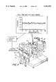
- FIG. 2is a perspective view of a cluster tool system embodying, and adapted for carrying out, the method of the invention
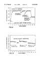
- FIG. 3comprises two graphic presentations of data, the character of which is noted thereon;
- FIG. 4is a functional block diagram of integrated sensor and cell control software suitable for use in the method, system, and apparatus of the invention.
- FIGS. 5 through 9are graphic presentations of data, the specific character of which is noted adjacent each figure.
- FIG. 2illustrates the Applied Materials CENTURA cluster tool, showing two loadlocks 10 and 12, a central robotic transfer chamber 14, process chambers 16 and 18, and a cooldown chamber 20.
- An On-Line Technologies integrated Fourier transform infrared film thickness monitor 22is mounted on top of the cooldown chamber 20.
- the EPI CENTURA reactoris a state of the art production tool for the fabrication of doped epitaxial silicon layers, typically grown on heavily doped or ion implanted substrate wafers.
- a typical depositiontakes about 100 seconds, and the throughput for a system can be in the range of 30 wafers per hour.
- Process variablesinclude gas flows, gas dilution (typically with hydrogen), temperature history, and deposition time; the high thermal ramp rates enabled by quartz lamp wafer heating make the EPI CENTURA a rapid thermal process tool.
- the EPI CENTURAis also an extremely stable reactor. Excursions in deposition conditions can be largely ignored within a single deposition run and, generally speaking, the wafer-to-wafer reproducibility of the process is extremely high. Because of these features the process is well suited to a run-to-run control system.
- the senoris mounted on the cooldown chamber, thus enabling implementation of the instant system without affecting the design or operation of the deposition process chambers at all, which is a key practical advantage; moreover because, in such an embodiment, the measurements are advantageously performed during the normal cooldown process of the tool, metrology and control are implemented with no affect on the tool throughput or process cycle time.
- the On-Line Technologies film thickness monitorwhich is desirably employed as the sensor means consists of an FTIR spectrophotometer configured for reflectance measurements, a reference mirror mounted in the cooldown and metrology chamber of the cluster tool, and a controller with software to perform data acquisition and analysis.
- the analysis algorithmsare based on a model based analysis of the reflectance that fits a simulated reflectance spectrum to the measured data, as taught for example in Liu et al. U.S. Pat. No. 5,604,581.
- the fitting parameterswhich include variables such as film thickness, epi/substrate doping transition width, and substrate carrier concentration, are selected to provide an accurate and relatively complete description of the optical properties of the wafers using only a few free parameters.
- FIG. 3illustrates model based fits for two epi samples, including one (FIG. 3(b)) that is well under one micron.
- the layer thickness, the substrate carrier density, and the doping transition widthwere varied for the fits.
- the peak in FIG. 3(b) at 2350 wavenumbersis due to atmospheric CO 2 in the optical path.
- FIG. 3illustrates the excellent accuracy with which the reflectance model accounts for the quantitative aspects of the epi silicon optical properties.
- the epitaxial thickness sensoris fully automated. Data are collected, analyzed, and archived without operator interaction.
- the cluster tool robotprovides wafer handling to load and unload wafers. Calibration is automated as well, and employs a standard reference material mounted within the cooldown chamber, allowing for frequent and non-interfering corrections for spectrometer drift.
- the functional modules of the preferred systemare shown as a block diagram in FIG. 5.
- the sensorperforms measurements on each wafer as it passes through the cooldown chamber.
- the sensor data analysis moduleperforms a model based analysis of the spectrum (or spectra, in those instances in which the system of the invention is constructed and configured for the collection of data from multiple measurement points) to extract the epitaxial layer thickness.
- the run-to-run control modulereceives the data, and analyzes the data for drifts. If a drift is detected the controller uses a reactor model to compute a recipe update for the next wafer, which compensates for the drift, and sends the updated recipe to the cell coordinator, which routes the new recipe to the cluster tool via the SECS port.
- the graphical user interfacepresents the data in control chart or spreadsheet format.
- the preferred systememploys a linear exponentially weighted moving average (linear EWMA) controller.
- linear EWMAlinear exponentially weighted moving average
- this type of controlleris useful when a process has multiple control inputs as well as multiple outputs.
- the processmust be sufficiently stable that its control surface model can be linearized about a local operation point.
- the EWMA controllerwas used to estimate the rate, but the actual deposition rate was not controlled; rather, the deposition time was modified to compensate for drifts in the rate.
- y r [n]represents a p by 1 vector of model outputs
- nindicates a discrete "run” of the process
- Arepresents a p by q fixed "gain” matrix from the q by 1 vector of process inputs
- x[n]represents a p by 1 vector of model offsets.
- the offset vectoris updated using the vector of measured outputs, y r [n], to obtain a vector of measured offset terms
- EWMAexponentially weighted moving average
- This updateconstitutes a smoothing (or filtering) of measurements of the offset term in order to adapt the process model to account for recent changes in the process.
- the amount of smoothing performed for the i th outputis a function of the EWMA weight, w i . Higher weights indicate recent measurements are weighted more in each update, and therefore indicate less filtering.
- This methodis effective for many processes in the semiconductor industry; this is so because many processes are subject to small shift or drift offset changes in the overall equipment state, but the underlying process dependencies (gain matrix entries) do not change.
- the epitaxial silicon processis a good example of this type of drift disturbance. However, the drift rate is relatively independent of the process settings (within a neighborhood around the optimal setting).
- the EWMA run to run controlleruses the above estimation scheme to track the process parameters of drifting or shifting processes.
- a typical parametermight be the deposition rate of a particular process.
- the controllerthen utilizes this updated process model to make changes to the processing recipes.
- the controllermight adjust the equipment settings, x[n], such that the deposition rate is controlled to a specified value. This is done by substituting the desired output in for y[n] in (1), and solving the equations for the process settings, x[n]. For multiple inputs and multiple outputs, this solution process may be quite complicated, and often requires the use of very stable linear solvers.
- a second method for controlwhich has been employed in this work, is to utilize the updated model for the deposition rate to make changes to the deposition time.
- This control strategyis often used to reduce the amount of changes in the processing conditions or to simplify the control scheme.
- the deposition thickness, y t [n]is a function of the process rate, y t [r], and the deposition time, t[n],
- the controllerupdates the model for y r [n], substitutes the desired thickness in for y t [n], and then solves for the deposition time, t[n].
- the first batch of wafershaving an epi thickness of ⁇ 2.15 ⁇ m, the second a thickness of ⁇ 2.65 ⁇ m, the third a thickness of ⁇ 2.16 ⁇ m, and the fourth a thickness of ⁇ 2.6 ⁇ m.
- FIG. 6shows details for the first batch of wafers (wafers 0 to 74). As can be seen, one out of every three data points is different from the two others. This trend appears to be caused by one of the three chambers (the second) of the fabrication tool being slightly out of tune from the other two.
- the repetitive patterni.e., thickness equal to ⁇ 2.16 ⁇ m, ⁇ 2.14 ⁇ m, ⁇ 2.16 ⁇ m and repeat
- the sequence variationsare attributed to temporary pauses in the tool operation, which allowed the system to reset its chamber sequence.
- FIG. 7shows the results for the second batch of wafers (wafers 75 to 537).
- the threefold periodicity in the datawas observed without interruption for this entire sequence.
- the wafers with the different (in this case higher) epi thicknesscorrespond, as in the case of the first batch, to the second chamber.
- an upward drift in the thicknessoccurs as a function of time, while no significant drift was seen for the wafers of the two other chambers (at least in the region comprised of wafer #300 to wafer #537).
- FIGS. 5-7show that: 1) the sensor provided reliable thickness results for nearly all of the wafers during an extended process run, and 2) drift within the different cluster tool process chambers occurred and were identifiable from the sensor data. In particular, during these runs the second chamber seems to have behaved slightly differently from the two others and, in some cases, to produce a noticeable drift in thickness with time.
- Control runswere carried out by processing a similar series of wafers in a single chamber system while the run-to-run controller was enabled. For these experiments a setpoint was specified for thickness.
- the run-to-run controllerestimated the current deposition rate by performing an exponentially weighted moving average of the measured thickness on the previously processed wafers.
- the deposition timewas updated after each wafer was processed.
- the new deposition timewas calculated as the target thickness divided by the EWMA estimated rate.
- the recipe changeswere automatically downloaded to the cluster tool via the SECS port after each measurement. Process upsets were simulated by deliberately modifying the temperature in the recipe during the process.
- the performance of the system under run-to-run control, as it reacquired the target thickness values,is shown in FIG. 8.
- the systemwas started running an epi recipe for films of 4.5 microns, substantially thinner than the target thickness of six microns entered into the run-to-run control module. Within four wafers the controller reached steady state at the target thickness. The deposition time after capture of target thickness was 100 seconds.
- a small process upsetwas simulated starting at wafer 9. For this simulated process upset the recipe was modified so as to increase the growth temperature by 15° C. This resulted in a change in growth rate of less than 1%. Because the granularity of the deposition time parameter is 1%, roundoff resulted in no modification to the recipe.
- the run-to-run controllerdesirably uses an exponentially weighted moving average to provide a smoothed estimate the rate.
- the ⁇ parameter which determines relative weight of each previous samplewas set to 0.7. This value of ⁇ was consistent with the observed behavior, i.e., that it took four samples to recover from a discontinuous process upset.
- a second set of waferswere processed to assess the stability of the process while under run-to-run control, the results of which are shown in FIG. 9.
- the first six waferswere used to estimate the film thickness associated with the chosen recipe.
- an unscheduled shut downdue to a scrubber fault
- two more waferswere processed under open loop control; it is to be noted that the film thickness drifted for these two wafers.
- the target thickness calculated from the average thickness of the first six waferswas used as the setpoint for the second eight wafers processed with the run-to-run control module enabled.
- the last eight waferswere then processed with the run-to-run control disabled.
- a primary benefit of closed loop control for the instant processlies in improved overall equipment effectiveness, estimated to be about 22% for embodiments such as that described.
- a 50% reduction of monitor wafer usageis believed to be likely, and is itself a powerful driver for this technology.
- a modern 200 mm epi line producing 50,000 wafers per monthtypically allocates 4% of its production capacity to monitor wafers which are not sold.
- the present inventionprovides a novel cell control method, apparatus, and system whereby and wherein trends of departures from target values of one or more properties of semiconductor wafers can be detected in line and during fabrication, and whereby and wherein adjustments can be made in processing conditions so as to minimize or eliminate (or, at least, reduce) such departures in wafers subsequently fabricated.
- the method, apparatus, and system of the inventionare especially well suited for the fabrication of semiconductor wafers on a production basis, and they enable measurement and control of many properties that are essential to satisfactory wafer performance, especially layer thickness and composition; these advantages are due largely to the robustness and broad range of measurement capabilities of the FTIR sensor.
- successful closed-loop control of an epitaxial silicon deposition processis demonstrated on a commercial, single wafer cluster tool using an integrated FTIR spectrometer mounted on the cluster tool cooldown chamber and a software package incorporating a run-to-run control algorithm, in which process recipe modifications to the process are computed and uploaded to the cluster tool automatically using the SECS communication port, and process drifts and chamber-to-chamber differences in the silicon film thickness are monitored over an extended process run using the integrated thickness monitor.
- the feasibility of using wafer-state feedback to control the fabrication process for epitaxial siliconis also demonstrated, and indicates that significant improvements in overall equipment effectiveness, and reductions in production costs, can be obtained through use of the technology disclosed.
Landscapes
- Chemical & Material Sciences (AREA)
- Engineering & Computer Science (AREA)
- Organic Chemistry (AREA)
- Metallurgy (AREA)
- Mechanical Engineering (AREA)
- Materials Engineering (AREA)
- Chemical Kinetics & Catalysis (AREA)
- General Physics & Mathematics (AREA)
- Power Engineering (AREA)
- Microelectronics & Electronic Packaging (AREA)
- General Chemical & Material Sciences (AREA)
- Computer Hardware Design (AREA)
- Manufacturing & Machinery (AREA)
- Condensed Matter Physics & Semiconductors (AREA)
- Physics & Mathematics (AREA)
- Automation & Control Theory (AREA)
- Chemical Vapour Deposition (AREA)
- Testing Or Measuring Of Semiconductors Or The Like (AREA)
Abstract
Description
______________________________________ Sensor Driven Closed Loop Control Fixed Set Point Control ______________________________________ Immediate measurements on every wafer Delayed measurements No extra wafer handling Sporadic measurements Automatic closed loop control Extra wafer handling Potential Overall Equipment Effectiveness Operator required (OEE) about 57% OEE about 30% Tighter product specification Looser specifications ______________________________________
y.sub.r [n]=Ax[n]+b[n]
b[n]=y.sub.r [n]-Ax[n],
b[n+1]=Wb[n]+(I-W)b[n],
y.sub.t [n]=y.sub.r [n]·t[n].
Claims (13)
Priority Applications (3)
| Application Number | Priority Date | Filing Date | Title |
|---|---|---|---|
| US09/156,277US6161054A (en) | 1997-09-22 | 1998-09-17 | Cell control method and apparatus |
| AU22476/99AAU2247699A (en) | 1997-09-22 | 1998-09-18 | Cell control method and apparatus |
| PCT/US1998/019598WO1999015710A1 (en) | 1997-09-22 | 1998-09-18 | Cell control method and apparatus |
Applications Claiming Priority (2)
| Application Number | Priority Date | Filing Date | Title |
|---|---|---|---|
| US5943597P | 1997-09-22 | 1997-09-22 | |
| US09/156,277US6161054A (en) | 1997-09-22 | 1998-09-17 | Cell control method and apparatus |
Publications (1)
| Publication Number | Publication Date |
|---|---|
| US6161054Atrue US6161054A (en) | 2000-12-12 |
Family
ID=26738745
Family Applications (1)
| Application Number | Title | Priority Date | Filing Date |
|---|---|---|---|
| US09/156,277Expired - LifetimeUS6161054A (en) | 1997-09-22 | 1998-09-17 | Cell control method and apparatus |
Country Status (3)
| Country | Link |
|---|---|
| US (1) | US6161054A (en) |
| AU (1) | AU2247699A (en) |
| WO (1) | WO1999015710A1 (en) |
Cited By (92)
| Publication number | Priority date | Publication date | Assignee | Title |
|---|---|---|---|---|
| US6282459B1 (en)* | 1998-09-01 | 2001-08-28 | International Business Machines Corporation | Structure and method for detection of physical interference during transport of an article |
| US20010024691A1 (en)* | 1999-12-24 | 2001-09-27 | Norio Kimura | Semiconductor substrate processing apparatus and method |
| US6336055B1 (en)* | 1998-01-14 | 2002-01-01 | Samsung Electronics Co., Ltd. | Method for controlling unit operating states of semiconductor fabricating equipment arranged in a processing line |
| US6410351B1 (en)* | 2000-07-13 | 2002-06-25 | Advanced Micro Devices, Inc. | Method and apparatus for modeling thickness profiles and controlling subsequent etch process |
| US6424876B1 (en)* | 1999-07-22 | 2002-07-23 | Advanced Micro Devices, Inc. | Statistical process control system with normalized control charting |
| US6467077B1 (en)* | 1999-07-14 | 2002-10-15 | Nec Electronics, Inc. | Capturing an evolving wafer fabrication method and system |
| US20030060917A1 (en)* | 2001-09-25 | 2003-03-27 | Dainippon Screen Mfg. Co., Ltd. | Substrate processing apparatus control system and substrate processing apparatus |
| WO2003033763A1 (en)* | 2001-10-17 | 2003-04-24 | Aixtron Ag | Method and device for monitoring a cvd process |
| US6560504B1 (en)* | 1999-09-29 | 2003-05-06 | Advanced Micro Devices, Inc. | Use of contamination-free manufacturing data in fault detection and classification as well as in run-to-run control |
| US6567717B2 (en)* | 2000-01-19 | 2003-05-20 | Advanced Micro Devices, Inc. | Feed-forward control of TCI doping for improving mass-production-wise, statistical distribution of critical performance parameters in semiconductor devices |
| US6574525B1 (en) | 2002-03-25 | 2003-06-03 | Lsi Logic Corporation | In situ measurement |
| US20030106642A1 (en)* | 2001-07-10 | 2003-06-12 | Applied Materials, Inc. | Semiconductor processing module with integrated feedback/feed forward metrology |
| US6604012B1 (en)* | 1999-10-23 | 2003-08-05 | Samsung Electronics Co., Ltd. | Lots dispatching method for variably arranging processing equipment and/or processing conditions in a succeeding process according to the results of a preceding process and apparatus for the same |
| US20030165755A1 (en)* | 2002-03-01 | 2003-09-04 | Applied Materials, Inc. | Methodology for repeatable post etch CD in a production tool |
| US6625512B1 (en)* | 2000-07-25 | 2003-09-23 | Advanced Micro Devices, Inc. | Method and apparatus for performing final critical dimension control |
| US6625513B1 (en)* | 2000-08-15 | 2003-09-23 | Applied Materials, Inc. | Run-to-run control over semiconductor processing tool based upon mirror image target |
| WO2003085586A1 (en)* | 2002-03-29 | 2003-10-16 | Timbre Technologies, Inc. | Metrology diffraction signal adaptation for tool-to-tool matching |
| US6640151B1 (en) | 1999-12-22 | 2003-10-28 | Applied Materials, Inc. | Multi-tool control system, method and medium |
| US6662070B1 (en)* | 2000-03-08 | 2003-12-09 | Advanced Micro Devices, Inc. | Wafer rotation randomization in cluster tool processing |
| US20030228532A1 (en)* | 2002-03-01 | 2003-12-11 | Applied Materials, Inc. | Method and apparatus for controlling etch processes during fabrication of semiconductor devices |
| US6664557B1 (en)* | 2001-03-19 | 2003-12-16 | Lam Research Corporation | In-situ detection of thin-metal interface using optical interference |
| US20040007325A1 (en)* | 2002-06-11 | 2004-01-15 | Applied Materials, Inc. | Integrated equipment set for forming a low K dielectric interconnect on a substrate |
| US20040015794A1 (en)* | 2002-03-12 | 2004-01-22 | Toshiya Kotani | Method of setting process parameter and method of setting process parameter and/or design rule |
| US6694275B1 (en)* | 2000-06-02 | 2004-02-17 | Timbre Technologies, Inc. | Profiler business model |
| US20040040001A1 (en)* | 2002-08-22 | 2004-02-26 | Miller Michael L. | Method and apparatus for predicting device electrical parameters during fabrication |
| US6708074B1 (en) | 2000-08-11 | 2004-03-16 | Applied Materials, Inc. | Generic interface builder |
| US6725402B1 (en)* | 2000-07-31 | 2004-04-20 | Advanced Micro Devices, Inc. | Method and apparatus for fault detection of a processing tool and control thereof using an advanced process control (APC) framework |
| US6728591B1 (en)* | 2001-08-01 | 2004-04-27 | Advanced Micro Devices, Inc. | Method and apparatus for run-to-run control of trench profiles |
| US20040092047A1 (en)* | 2002-11-12 | 2004-05-13 | Applied Materials,Inc. | Method and apparatus employing integrated metrology for improved dielectric etch efficiency |
| US20040203177A1 (en)* | 2003-04-11 | 2004-10-14 | Applied Materials, Inc. | Method and system for monitoring an etch process |
| US20040200574A1 (en)* | 2003-04-11 | 2004-10-14 | Applied Materials, Inc. | Method for controlling a process for fabricating integrated devices |
| US20040206621A1 (en)* | 2002-06-11 | 2004-10-21 | Hongwen Li | Integrated equipment set for forming a low K dielectric interconnect on a substrate |
| US20040215365A1 (en)* | 2001-08-28 | 2004-10-28 | Asami Obara | Processing system |
| US20040225396A1 (en)* | 2002-11-12 | 2004-11-11 | Jorn Maeritz | Method, device, computer-readable memory and computer program element for the computer-aided monitoring and controlling of a manufacturing process |
| US20050032250A1 (en)* | 2003-08-06 | 2005-02-10 | Applied Materials, Inc. | Chamber stability monitoring using an integrated metrology tool |
| US20050059251A1 (en)* | 2003-09-12 | 2005-03-17 | Taiwan Semicondutor Manufacturing Co. | Constant and reducible hole bottom CD in variable post-CMP thickness and after-development-inspection CD |
| US20050064714A1 (en)* | 2003-09-19 | 2005-03-24 | Applied Materials, Inc. | Method for controlling critical dimensions during an etch process |
| US20050064719A1 (en)* | 2003-09-19 | 2005-03-24 | Applied Materials, Inc. | Method of controlling critical dimension microloading of photoresist trimming process by selective sidewall polymer deposition |
| US20050085090A1 (en)* | 2003-10-21 | 2005-04-21 | Applied Materials, Inc. | Method for controlling accuracy and repeatability of an etch process |
| US6890773B1 (en)* | 2002-04-19 | 2005-05-10 | Advanced Micro Devices, Inc. | Dynamic maintenance of manufacturing system components |
| US20050118812A1 (en)* | 2001-12-31 | 2005-06-02 | Tokyo Elecron Limited | Method of detecting, identifying and correcting process performance |
| US6907308B1 (en)* | 2002-08-02 | 2005-06-14 | Advanced Micro Devices, Inc. | Remote wafer flow and recipe editor for simiconductor processing control |
| US6912433B1 (en)* | 2002-12-18 | 2005-06-28 | Advanced Mirco Devices, Inc. | Determining a next tool state based on fault detection information |
| US6910947B2 (en) | 2001-06-19 | 2005-06-28 | Applied Materials, Inc. | Control of chemical mechanical polishing pad conditioner directional velocity to improve pad life |
| US6913938B2 (en) | 2001-06-19 | 2005-07-05 | Applied Materials, Inc. | Feedback control of plasma-enhanced chemical vapor deposition processes |
| US6950716B2 (en) | 2001-08-13 | 2005-09-27 | Applied Materials, Inc. | Dynamic control of wafer processing paths in semiconductor manufacturing processes |
| US6961636B1 (en)* | 2001-04-19 | 2005-11-01 | Advanced Micro Devices Inc. | Method and apparatus for dynamically monitoring controller tuning parameters |
| US6961626B1 (en) | 2004-05-28 | 2005-11-01 | Applied Materials, Inc | Dynamic offset and feedback threshold |
| US6984198B2 (en) | 2001-08-14 | 2006-01-10 | Applied Materials, Inc. | Experiment management system, method and medium |
| US20060009872A1 (en)* | 2004-07-08 | 2006-01-12 | Timbre Technologies, Inc. | Optical metrology model optimization for process control |
| US6999836B2 (en) | 2002-08-01 | 2006-02-14 | Applied Materials, Inc. | Method, system, and medium for handling misrepresentative metrology data within an advanced process control system |
| US7043319B1 (en)* | 2003-09-30 | 2006-05-09 | National Semiconductor Corporation | System and method for visualizing the use of resources in a process system |
| US7047099B2 (en) | 2001-06-19 | 2006-05-16 | Applied Materials Inc. | Integrating tool, module, and fab level control |
| US7069103B1 (en)* | 2002-06-28 | 2006-06-27 | Advanced Micro Devices, Inc. | Controlling cumulative wafer effects |
| US7069101B1 (en) | 1999-07-29 | 2006-06-27 | Applied Materials, Inc. | Computer integrated manufacturing techniques |
| US20060154388A1 (en)* | 2005-01-08 | 2006-07-13 | Richard Lewington | Integrated metrology chamber for transparent substrates |
| US7082345B2 (en)* | 2001-06-19 | 2006-07-25 | Applied Materials, Inc. | Method, system and medium for process control for the matching of tools, chambers and/or other semiconductor-related entities |
| US7096085B2 (en) | 2004-05-28 | 2006-08-22 | Applied Materials | Process control by distinguishing a white noise component of a process variance |
| US7101799B2 (en) | 2001-06-19 | 2006-09-05 | Applied Materials, Inc. | Feedforward and feedback control for conditioning of chemical mechanical polishing pad |
| US20070005172A1 (en)* | 2005-06-30 | 2007-01-04 | Hans-Juergen Malig | Method and system for advanced process control using measurement uncertainty as control input |
| US7160739B2 (en) | 2001-06-19 | 2007-01-09 | Applied Materials, Inc. | Feedback control of a chemical mechanical polishing device providing manipulation of removal rate profiles |
| US7188142B2 (en) | 2000-11-30 | 2007-03-06 | Applied Materials, Inc. | Dynamic subject information generation in message services of distributed object systems in a semiconductor assembly line facility |
| US20070078556A1 (en)* | 2005-09-30 | 2007-04-05 | Stirton James B | Method and system for advanced process control using a combination of weighted relative bias values |
| US7201936B2 (en) | 2001-06-19 | 2007-04-10 | Applied Materials, Inc. | Method of feedback control of sub-atmospheric chemical vapor deposition processes |
| US7205228B2 (en) | 2003-06-03 | 2007-04-17 | Applied Materials, Inc. | Selective metal encapsulation schemes |
| US20070099570A1 (en)* | 2005-10-31 | 2007-05-03 | Silicon Laboratories, Inc. | Receiver with multi-tone wideband I/Q mismatch calibration and method therefor |
| US20070097383A1 (en)* | 2005-01-08 | 2007-05-03 | Nguyen Khiem K | Method and apparatus for integrating metrology with etch processing |
| US7225047B2 (en) | 2002-03-19 | 2007-05-29 | Applied Materials, Inc. | Method, system and medium for controlling semiconductor wafer processes using critical dimension measurements |
| US7250373B2 (en) | 2004-08-27 | 2007-07-31 | Applied Materials, Inc. | Method and apparatus for etching material layers with high uniformity of a lateral etch rate across a substrate |
| US7272459B2 (en) | 2002-11-15 | 2007-09-18 | Applied Materials, Inc. | Method, system and medium for controlling manufacture process having multivariate input parameters |
| US20070229855A1 (en)* | 2006-03-30 | 2007-10-04 | Timbre Technologies, Inc. | In-die optical metrology |
| US20070239285A1 (en)* | 2006-04-06 | 2007-10-11 | Good Richard P | Time weighted moving average filter |
| US20070239633A1 (en)* | 2006-03-29 | 2007-10-11 | Honeywell International, Inc. | Empirical design of experiments using neural network models |
| US20070282554A1 (en)* | 2006-05-31 | 2007-12-06 | Tokyo Electron Limited | Information processing apparatus, semiconductor manufacturing system, information processing method, and storage medium |
| US7333871B2 (en) | 2003-01-21 | 2008-02-19 | Applied Materials, Inc. | Automated design and execution of experiments with integrated model creation for semiconductor manufacturing tools |
| US7337019B2 (en) | 2001-07-16 | 2008-02-26 | Applied Materials, Inc. | Integration of fault detection with run-to-run control |
| US7340318B1 (en)* | 2002-12-20 | 2008-03-04 | Advanced Micro Devices, Inc. | Method and apparatus for assessing controller performance |
| US7354332B2 (en) | 2003-08-04 | 2008-04-08 | Applied Materials, Inc. | Technique for process-qualifying a semiconductor manufacturing tool using metrology data |
| US7356377B2 (en) | 2004-01-29 | 2008-04-08 | Applied Materials, Inc. | System, method, and medium for monitoring performance of an advanced process control system |
| US20080147224A1 (en)* | 2006-10-09 | 2008-06-19 | James Broc Stirton | Method and Apparatus for Compensating Metrology Data for Site Bias Prior to Filtering |
| US20080155443A1 (en)* | 2003-11-10 | 2008-06-26 | Pannese Patrick D | Methods and systems for controlling a semiconductor fabrication process |
| US20080155442A1 (en)* | 2003-11-10 | 2008-06-26 | Pannese Patrick D | Methods and systems for controlling a semiconductor fabrication process |
| US20080163094A1 (en)* | 2003-11-10 | 2008-07-03 | Pannese Patrick D | Methods and systems for controlling a semiconductor fabrication process |
| US20080243271A1 (en)* | 2007-03-30 | 2008-10-02 | Ram Gandikota | System and method for quantifying an improvement in an advanced process control strategy |
| US20080251007A1 (en)* | 2007-04-13 | 2008-10-16 | Texas Instruments Deutschland Gmbh | Method of controlling an epitaxial growth process in an epitaxial reactor |
| US20080294280A1 (en)* | 2006-01-30 | 2008-11-27 | Nikon Corporation | Processing condition determining method and apparatus, display method and apparatus, processing apparatus, measurement apparatus and exposure apparatus, substrate processing system, and program and information recording medium |
| US20090138114A1 (en)* | 2005-05-11 | 2009-05-28 | Richard Gerard Burda | Method of release and product flow management for a manufacturing facility |
| US7698012B2 (en) | 2001-06-19 | 2010-04-13 | Applied Materials, Inc. | Dynamic metrology schemes and sampling schemes for advanced process control in semiconductor processing |
| US8005634B2 (en) | 2002-03-22 | 2011-08-23 | Applied Materials, Inc. | Copper wiring module control |
| CN101055422B (en)* | 2006-04-14 | 2012-05-02 | 应用材料公司 | Integrated measuring chamber for transparent substrates |
| US11300948B2 (en)* | 2019-06-27 | 2022-04-12 | Nova Ltd | Process control of semiconductor fabrication based on spectra quality metrics |
| US20240369996A1 (en)* | 2023-03-29 | 2024-11-07 | Ats Corporation | Systems and methods for maintaining a record for a workpiece processed by a computer numerically controlled (cnc) electronically synchronized manufacturing assembly line cell |
Families Citing this family (14)
| Publication number | Priority date | Publication date | Assignee | Title |
|---|---|---|---|---|
| JP2002517740A (en)* | 1998-06-12 | 2002-06-18 | オン−ライン テクノロジーズ インコーポレーテッド | Method and apparatus for identifying process chamber clean or wafer etching endpoints |
| US7295314B1 (en) | 1998-07-10 | 2007-11-13 | Nanometrics Incorporated | Metrology/inspection positioning system |
| US6320609B1 (en) | 1998-07-10 | 2001-11-20 | Nanometrics Incorporated | System using a polar coordinate stage and continuous image rotation to compensate for stage rotation |
| US7020537B2 (en) | 1999-04-13 | 2006-03-28 | Semitool, Inc. | Tuning electrodes used in a reactor for electrochemically processing a microelectronic workpiece |
| US7189318B2 (en) | 1999-04-13 | 2007-03-13 | Semitool, Inc. | Tuning electrodes used in a reactor for electrochemically processing a microelectronic workpiece |
| WO2001040538A1 (en)* | 1999-12-03 | 2001-06-07 | The Regents Of The University Of California | Method and system relating to thickness control of film vapor deposition |
| ATE287552T1 (en) | 2000-01-29 | 2005-02-15 | Abb Research Ltd | SYSTEM AND METHOD FOR DETERMINING PRODUCTION SYSTEM EFFECTIVENESS, ERROR EVENTS AND CAUSES OF ERROR |
| WO2001090434A2 (en)* | 2000-05-24 | 2001-11-29 | Semitool, Inc. | Tuning electrodes used in a reactor for electrochemically processing a microelectronic workpiece |
| US6218200B1 (en)* | 2000-07-14 | 2001-04-17 | Motorola, Inc. | Multi-layer registration control for photolithography processes |
| EP1184763A1 (en)* | 2000-08-24 | 2002-03-06 | Infineon Technologies SC300 GmbH & Co. KG | Arrangement for data transmission between an equipment for manufacturing of a semiconductor device and a communicating device and method for operating the arrangement |
| WO2002023289A2 (en)* | 2000-09-15 | 2002-03-21 | Advanced Micro Devices, Inc. | Adaptive sampling method for improved control in semiconductor manufacturing |
| DE10124609B4 (en)* | 2001-05-17 | 2012-12-27 | Aixtron Se | Method for depositing active layers on substrates |
| US6842659B2 (en) | 2001-08-24 | 2005-01-11 | Applied Materials Inc. | Method and apparatus for providing intra-tool monitoring and control |
| JP4068327B2 (en)* | 2001-10-11 | 2008-03-26 | 株式会社東芝 | Semiconductor manufacturing apparatus and semiconductor device manufacturing method |
Citations (12)
| Publication number | Priority date | Publication date | Assignee | Title |
|---|---|---|---|---|
| US5392118A (en)* | 1992-05-13 | 1995-02-21 | International Business Machines Corporation | Method for measuring a trench depth parameter of a material |
| US5604581A (en)* | 1994-10-07 | 1997-02-18 | On-Line Technologies, Inc. | Film thickness and free carrier concentration analysis method and apparatus |
| US5795356A (en)* | 1996-05-31 | 1998-08-18 | Slsp Partners, Inc. | Microelectronic component fabrication facility, and process for making and using the facility |
| US5846849A (en)* | 1993-02-04 | 1998-12-08 | Cornell Research Foundation, Inc. | Microstructure and single mask, single-crystal process for fabrication thereof |
| US5900633A (en)* | 1997-12-15 | 1999-05-04 | On-Line Technologies, Inc | Spectrometric method for analysis of film thickness and composition on a patterned sample |
| US5926690A (en)* | 1997-05-28 | 1999-07-20 | Advanced Micro Devices, Inc. | Run-to-run control process for controlling critical dimensions |
| US5930586A (en)* | 1997-07-03 | 1999-07-27 | Motorola, Inc. | Method and apparatus for in-line measuring backside wafer-level contamination of a semiconductor wafer |
| US5948958A (en)* | 1998-09-01 | 1999-09-07 | Applied Materials, Inc. | Method and apparatus for verifying the calibration of semiconductor processing equipment |
| US5951770A (en)* | 1997-06-04 | 1999-09-14 | Applied Materials, Inc. | Carousel wafer transfer system |
| US5957648A (en)* | 1996-12-11 | 1999-09-28 | Applied Materials, Inc. | Factory automation apparatus and method for handling, moving and storing semiconductor wafer carriers |
| US5964561A (en)* | 1996-12-11 | 1999-10-12 | Applied Materials, Inc. | Compact apparatus and method for storing and loading semiconductor wafer carriers |
| US6073501A (en)* | 1997-06-20 | 2000-06-13 | Advanced Micro Devices, Inc. | Apparatus and method for semiconductor wafer processing which facilitate determination of a source of contaminants or defects |
Family Cites Families (1)
| Publication number | Priority date | Publication date | Assignee | Title |
|---|---|---|---|---|
| US4772485A (en)* | 1983-10-05 | 1988-09-20 | Toshiba Kikai Kabushiki Kaisha | Process control system of semiconductor vapor phase growing apparatus |
- 1998
- 1998-09-17USUS09/156,277patent/US6161054A/ennot_activeExpired - Lifetime
- 1998-09-18WOPCT/US1998/019598patent/WO1999015710A1/enactiveApplication Filing
- 1998-09-18AUAU22476/99Apatent/AU2247699A/ennot_activeAbandoned
Patent Citations (13)
| Publication number | Priority date | Publication date | Assignee | Title |
|---|---|---|---|---|
| US5392118A (en)* | 1992-05-13 | 1995-02-21 | International Business Machines Corporation | Method for measuring a trench depth parameter of a material |
| US5846849A (en)* | 1993-02-04 | 1998-12-08 | Cornell Research Foundation, Inc. | Microstructure and single mask, single-crystal process for fabrication thereof |
| US6051866A (en)* | 1993-02-04 | 2000-04-18 | Cornell Research Foundation, Inc. | Microstructures and single mask, single-crystal process for fabrication thereof |
| US5604581A (en)* | 1994-10-07 | 1997-02-18 | On-Line Technologies, Inc. | Film thickness and free carrier concentration analysis method and apparatus |
| US5795356A (en)* | 1996-05-31 | 1998-08-18 | Slsp Partners, Inc. | Microelectronic component fabrication facility, and process for making and using the facility |
| US5957648A (en)* | 1996-12-11 | 1999-09-28 | Applied Materials, Inc. | Factory automation apparatus and method for handling, moving and storing semiconductor wafer carriers |
| US5964561A (en)* | 1996-12-11 | 1999-10-12 | Applied Materials, Inc. | Compact apparatus and method for storing and loading semiconductor wafer carriers |
| US5926690A (en)* | 1997-05-28 | 1999-07-20 | Advanced Micro Devices, Inc. | Run-to-run control process for controlling critical dimensions |
| US5951770A (en)* | 1997-06-04 | 1999-09-14 | Applied Materials, Inc. | Carousel wafer transfer system |
| US6073501A (en)* | 1997-06-20 | 2000-06-13 | Advanced Micro Devices, Inc. | Apparatus and method for semiconductor wafer processing which facilitate determination of a source of contaminants or defects |
| US5930586A (en)* | 1997-07-03 | 1999-07-27 | Motorola, Inc. | Method and apparatus for in-line measuring backside wafer-level contamination of a semiconductor wafer |
| US5900633A (en)* | 1997-12-15 | 1999-05-04 | On-Line Technologies, Inc | Spectrometric method for analysis of film thickness and composition on a patterned sample |
| US5948958A (en)* | 1998-09-01 | 1999-09-07 | Applied Materials, Inc. | Method and apparatus for verifying the calibration of semiconductor processing equipment |
Non-Patent Citations (6)
| Title |
|---|
| Dance. et al., "Modeling HTE Cost of Ownership of Assembly and Inspection", IEEE., pp. 57-60, 1996. |
| Dance. et al., Modeling HTE Cost of Ownership of Assembly and Inspection , IEEE., pp. 57 60, 1996.* |
| Dance., "Modeling HTE Cost of Ownership of Assembly and Inspection", IEEE., pp. 51-54, 1995. |
| Dance., Modeling HTE Cost of Ownership of Assembly and Inspection , IEEE., pp. 51 54, 1995.* |
| Janiak et al., "Investigation of Macroscopic Uniformity During CH/sub 4//H/sub2 Reactive Ion Etching of InP and Improvement Using a Quard Ring", IEEE., pp. 111-114, 1996. |
| Janiak et al., Investigation of Macroscopic Uniformity During CH/sub 4//H/sub2 Reactive Ion Etching of InP and Improvement Using a Quard Ring , IEEE., pp. 111 114, 1996.* |
Cited By (154)
| Publication number | Priority date | Publication date | Assignee | Title |
|---|---|---|---|---|
| US6336055B1 (en)* | 1998-01-14 | 2002-01-01 | Samsung Electronics Co., Ltd. | Method for controlling unit operating states of semiconductor fabricating equipment arranged in a processing line |
| US6282459B1 (en)* | 1998-09-01 | 2001-08-28 | International Business Machines Corporation | Structure and method for detection of physical interference during transport of an article |
| US6467077B1 (en)* | 1999-07-14 | 2002-10-15 | Nec Electronics, Inc. | Capturing an evolving wafer fabrication method and system |
| US6424876B1 (en)* | 1999-07-22 | 2002-07-23 | Advanced Micro Devices, Inc. | Statistical process control system with normalized control charting |
| US7174230B2 (en) | 1999-07-29 | 2007-02-06 | Applied Materials, Inc. | Computer integrated manufacturing techniques |
| US7069101B1 (en) | 1999-07-29 | 2006-06-27 | Applied Materials, Inc. | Computer integrated manufacturing techniques |
| US6560504B1 (en)* | 1999-09-29 | 2003-05-06 | Advanced Micro Devices, Inc. | Use of contamination-free manufacturing data in fault detection and classification as well as in run-to-run control |
| US6604012B1 (en)* | 1999-10-23 | 2003-08-05 | Samsung Electronics Co., Ltd. | Lots dispatching method for variably arranging processing equipment and/or processing conditions in a succeeding process according to the results of a preceding process and apparatus for the same |
| US6640151B1 (en) | 1999-12-22 | 2003-10-28 | Applied Materials, Inc. | Multi-tool control system, method and medium |
| US20010024691A1 (en)* | 1999-12-24 | 2001-09-27 | Norio Kimura | Semiconductor substrate processing apparatus and method |
| US6567717B2 (en)* | 2000-01-19 | 2003-05-20 | Advanced Micro Devices, Inc. | Feed-forward control of TCI doping for improving mass-production-wise, statistical distribution of critical performance parameters in semiconductor devices |
| US6662070B1 (en)* | 2000-03-08 | 2003-12-09 | Advanced Micro Devices, Inc. | Wafer rotation randomization in cluster tool processing |
| US6694275B1 (en)* | 2000-06-02 | 2004-02-17 | Timbre Technologies, Inc. | Profiler business model |
| US6410351B1 (en)* | 2000-07-13 | 2002-06-25 | Advanced Micro Devices, Inc. | Method and apparatus for modeling thickness profiles and controlling subsequent etch process |
| US6625512B1 (en)* | 2000-07-25 | 2003-09-23 | Advanced Micro Devices, Inc. | Method and apparatus for performing final critical dimension control |
| US6725402B1 (en)* | 2000-07-31 | 2004-04-20 | Advanced Micro Devices, Inc. | Method and apparatus for fault detection of a processing tool and control thereof using an advanced process control (APC) framework |
| US6708074B1 (en) | 2000-08-11 | 2004-03-16 | Applied Materials, Inc. | Generic interface builder |
| US6625513B1 (en)* | 2000-08-15 | 2003-09-23 | Applied Materials, Inc. | Run-to-run control over semiconductor processing tool based upon mirror image target |
| US7188142B2 (en) | 2000-11-30 | 2007-03-06 | Applied Materials, Inc. | Dynamic subject information generation in message services of distributed object systems in a semiconductor assembly line facility |
| US8504620B2 (en) | 2000-11-30 | 2013-08-06 | Applied Materials, Inc. | Dynamic subject information generation in message services of distributed object systems |
| US6664557B1 (en)* | 2001-03-19 | 2003-12-16 | Lam Research Corporation | In-situ detection of thin-metal interface using optical interference |
| US6961636B1 (en)* | 2001-04-19 | 2005-11-01 | Advanced Micro Devices Inc. | Method and apparatus for dynamically monitoring controller tuning parameters |
| US7783375B2 (en) | 2001-06-19 | 2010-08-24 | Applied Materials, Inc. | Dynamic metrology schemes and sampling schemes for advanced process control in semiconductor processing |
| US7047099B2 (en) | 2001-06-19 | 2006-05-16 | Applied Materials Inc. | Integrating tool, module, and fab level control |
| US7160739B2 (en) | 2001-06-19 | 2007-01-09 | Applied Materials, Inc. | Feedback control of a chemical mechanical polishing device providing manipulation of removal rate profiles |
| US7101799B2 (en) | 2001-06-19 | 2006-09-05 | Applied Materials, Inc. | Feedforward and feedback control for conditioning of chemical mechanical polishing pad |
| US8070909B2 (en) | 2001-06-19 | 2011-12-06 | Applied Materials, Inc. | Feedback control of chemical mechanical polishing device providing manipulation of removal rate profiles |
| US6913938B2 (en) | 2001-06-19 | 2005-07-05 | Applied Materials, Inc. | Feedback control of plasma-enhanced chemical vapor deposition processes |
| US8694145B2 (en) | 2001-06-19 | 2014-04-08 | Applied Materials, Inc. | Feedback control of a chemical mechanical polishing device providing manipulation of removal rate profiles |
| US7698012B2 (en) | 2001-06-19 | 2010-04-13 | Applied Materials, Inc. | Dynamic metrology schemes and sampling schemes for advanced process control in semiconductor processing |
| US7082345B2 (en)* | 2001-06-19 | 2006-07-25 | Applied Materials, Inc. | Method, system and medium for process control for the matching of tools, chambers and/or other semiconductor-related entities |
| US7725208B2 (en) | 2001-06-19 | 2010-05-25 | Applied Materials, Inc. | Dynamic metrology schemes and sampling schemes for advanced process control in semiconductor processing |
| US7201936B2 (en) | 2001-06-19 | 2007-04-10 | Applied Materials, Inc. | Method of feedback control of sub-atmospheric chemical vapor deposition processes |
| US6910947B2 (en) | 2001-06-19 | 2005-06-28 | Applied Materials, Inc. | Control of chemical mechanical polishing pad conditioner directional velocity to improve pad life |
| WO2003007365A3 (en)* | 2001-07-10 | 2003-08-28 | Applied Materials Inc | Semiconductor processing module with integrated feedback/feed forward metrology |
| US20030106642A1 (en)* | 2001-07-10 | 2003-06-12 | Applied Materials, Inc. | Semiconductor processing module with integrated feedback/feed forward metrology |
| US7337019B2 (en) | 2001-07-16 | 2008-02-26 | Applied Materials, Inc. | Integration of fault detection with run-to-run control |
| US6728591B1 (en)* | 2001-08-01 | 2004-04-27 | Advanced Micro Devices, Inc. | Method and apparatus for run-to-run control of trench profiles |
| US6950716B2 (en) | 2001-08-13 | 2005-09-27 | Applied Materials, Inc. | Dynamic control of wafer processing paths in semiconductor manufacturing processes |
| US6984198B2 (en) | 2001-08-14 | 2006-01-10 | Applied Materials, Inc. | Experiment management system, method and medium |
| US20040215365A1 (en)* | 2001-08-28 | 2004-10-28 | Asami Obara | Processing system |
| US7139627B2 (en)* | 2001-08-28 | 2006-11-21 | Tokyo Electron Limited | Calibration of plural processing systems |
| US6963789B2 (en)* | 2001-09-25 | 2005-11-08 | Dainippon Screen Mfg. Co., Ltd. | Substrate processing apparatus control system and substrate processing apparatus |
| US20030060917A1 (en)* | 2001-09-25 | 2003-03-27 | Dainippon Screen Mfg. Co., Ltd. | Substrate processing apparatus control system and substrate processing apparatus |
| WO2003033763A1 (en)* | 2001-10-17 | 2003-04-24 | Aixtron Ag | Method and device for monitoring a cvd process |
| US20040261704A1 (en)* | 2001-10-17 | 2004-12-30 | Michael Heuken | Method and device for monitoring a CVD-process |
| US20050118812A1 (en)* | 2001-12-31 | 2005-06-02 | Tokyo Elecron Limited | Method of detecting, identifying and correcting process performance |
| US20030228532A1 (en)* | 2002-03-01 | 2003-12-11 | Applied Materials, Inc. | Method and apparatus for controlling etch processes during fabrication of semiconductor devices |
| US6858361B2 (en) | 2002-03-01 | 2005-02-22 | David S. L. Mui | Methodology for repeatable post etch CD in a production tool |
| US7498106B2 (en) | 2002-03-01 | 2009-03-03 | Applied Materials, Inc. | Method and apparatus for controlling etch processes during fabrication of semiconductor devices |
| US20030165755A1 (en)* | 2002-03-01 | 2003-09-04 | Applied Materials, Inc. | Methodology for repeatable post etch CD in a production tool |
| US20060091108A1 (en)* | 2002-03-01 | 2006-05-04 | Applied Materials, Inc. | Method and apparatus for controlling etch processes during fabrication of semiconductor devices |
| US20050177811A1 (en)* | 2002-03-12 | 2005-08-11 | Kabushiki Kaisha Toshiba | Method of setting process parameter and method of setting process parameter and/or design rule |
| US7120882B2 (en) | 2002-03-12 | 2006-10-10 | Kabushiki Kaisha Toshiba | Method of setting process parameter and method of setting process parameter and/or design rule |
| US20040015794A1 (en)* | 2002-03-12 | 2004-01-22 | Toshiya Kotani | Method of setting process parameter and method of setting process parameter and/or design rule |
| US7181707B2 (en)* | 2002-03-12 | 2007-02-20 | Kabushiki Kaisha Toshiba | Method of setting process parameter and method of setting process parameter and/or design rule |
| US7225047B2 (en) | 2002-03-19 | 2007-05-29 | Applied Materials, Inc. | Method, system and medium for controlling semiconductor wafer processes using critical dimension measurements |
| US8005634B2 (en) | 2002-03-22 | 2011-08-23 | Applied Materials, Inc. | Copper wiring module control |
| US6574525B1 (en) | 2002-03-25 | 2003-06-03 | Lsi Logic Corporation | In situ measurement |
| US6792328B2 (en) | 2002-03-29 | 2004-09-14 | Timbre Technologies, Inc. | Metrology diffraction signal adaptation for tool-to-tool matching |
| WO2003085586A1 (en)* | 2002-03-29 | 2003-10-16 | Timbre Technologies, Inc. | Metrology diffraction signal adaptation for tool-to-tool matching |
| CN100399342C (en)* | 2002-03-29 | 2008-07-02 | 音质技术公司 | Metrology diffraction signal adaptation for tool-to-tool matching |
| US6890773B1 (en)* | 2002-04-19 | 2005-05-10 | Advanced Micro Devices, Inc. | Dynamic maintenance of manufacturing system components |
| US20040007325A1 (en)* | 2002-06-11 | 2004-01-15 | Applied Materials, Inc. | Integrated equipment set for forming a low K dielectric interconnect on a substrate |
| US20060246683A1 (en)* | 2002-06-11 | 2006-11-02 | Applied Materials, Inc. | Integrated equipment set for forming a low K dielectric interconnect on a substrate |
| US20040206621A1 (en)* | 2002-06-11 | 2004-10-21 | Hongwen Li | Integrated equipment set for forming a low K dielectric interconnect on a substrate |
| US7069103B1 (en)* | 2002-06-28 | 2006-06-27 | Advanced Micro Devices, Inc. | Controlling cumulative wafer effects |
| US6999836B2 (en) | 2002-08-01 | 2006-02-14 | Applied Materials, Inc. | Method, system, and medium for handling misrepresentative metrology data within an advanced process control system |
| US6907308B1 (en)* | 2002-08-02 | 2005-06-14 | Advanced Micro Devices, Inc. | Remote wafer flow and recipe editor for simiconductor processing control |
| US8185230B2 (en)* | 2002-08-22 | 2012-05-22 | Advanced Micro Devices, Inc. | Method and apparatus for predicting device electrical parameters during fabrication |
| US20040040001A1 (en)* | 2002-08-22 | 2004-02-26 | Miller Michael L. | Method and apparatus for predicting device electrical parameters during fabrication |
| US6909933B2 (en)* | 2002-11-12 | 2005-06-21 | Infineon Technologies Ag | Method, device, computer-readable memory and computer program element for the computer-aided monitoring and controlling of a manufacturing process |
| US20040225396A1 (en)* | 2002-11-12 | 2004-11-11 | Jorn Maeritz | Method, device, computer-readable memory and computer program element for the computer-aided monitoring and controlling of a manufacturing process |
| US20040092047A1 (en)* | 2002-11-12 | 2004-05-13 | Applied Materials,Inc. | Method and apparatus employing integrated metrology for improved dielectric etch efficiency |
| US7265382B2 (en) | 2002-11-12 | 2007-09-04 | Applied Materials, Inc. | Method and apparatus employing integrated metrology for improved dielectric etch efficiency |
| US7272459B2 (en) | 2002-11-15 | 2007-09-18 | Applied Materials, Inc. | Method, system and medium for controlling manufacture process having multivariate input parameters |
| US7966087B2 (en) | 2002-11-15 | 2011-06-21 | Applied Materials, Inc. | Method, system and medium for controlling manufacture process having multivariate input parameters |
| US6912433B1 (en)* | 2002-12-18 | 2005-06-28 | Advanced Mirco Devices, Inc. | Determining a next tool state based on fault detection information |
| US7340318B1 (en)* | 2002-12-20 | 2008-03-04 | Advanced Micro Devices, Inc. | Method and apparatus for assessing controller performance |
| US7333871B2 (en) | 2003-01-21 | 2008-02-19 | Applied Materials, Inc. | Automated design and execution of experiments with integrated model creation for semiconductor manufacturing tools |
| US20040200574A1 (en)* | 2003-04-11 | 2004-10-14 | Applied Materials, Inc. | Method for controlling a process for fabricating integrated devices |
| US20040203177A1 (en)* | 2003-04-11 | 2004-10-14 | Applied Materials, Inc. | Method and system for monitoring an etch process |
| US8257546B2 (en) | 2003-04-11 | 2012-09-04 | Applied Materials, Inc. | Method and system for monitoring an etch process |
| US7815812B2 (en) | 2003-04-11 | 2010-10-19 | Applied Materials, Inc. | Method for controlling a process for fabricating integrated devices |
| US7205228B2 (en) | 2003-06-03 | 2007-04-17 | Applied Materials, Inc. | Selective metal encapsulation schemes |
| US7354332B2 (en) | 2003-08-04 | 2008-04-08 | Applied Materials, Inc. | Technique for process-qualifying a semiconductor manufacturing tool using metrology data |
| US20050032250A1 (en)* | 2003-08-06 | 2005-02-10 | Applied Materials, Inc. | Chamber stability monitoring using an integrated metrology tool |
| US7482178B2 (en) | 2003-08-06 | 2009-01-27 | Applied Materials, Inc. | Chamber stability monitoring using an integrated metrology tool |
| US20050059251A1 (en)* | 2003-09-12 | 2005-03-17 | Taiwan Semicondutor Manufacturing Co. | Constant and reducible hole bottom CD in variable post-CMP thickness and after-development-inspection CD |
| US8207532B2 (en) | 2003-09-12 | 2012-06-26 | Taiwan Semiconductor Manufacturing Company | Constant and reducible hole bottom CD in variable post-CMP thickness and after-development-inspection CD |
| US6911399B2 (en) | 2003-09-19 | 2005-06-28 | Applied Materials, Inc. | Method of controlling critical dimension microloading of photoresist trimming process by selective sidewall polymer deposition |
| US20050064719A1 (en)* | 2003-09-19 | 2005-03-24 | Applied Materials, Inc. | Method of controlling critical dimension microloading of photoresist trimming process by selective sidewall polymer deposition |
| US20050064714A1 (en)* | 2003-09-19 | 2005-03-24 | Applied Materials, Inc. | Method for controlling critical dimensions during an etch process |
| US7043319B1 (en)* | 2003-09-30 | 2006-05-09 | National Semiconductor Corporation | System and method for visualizing the use of resources in a process system |
| US7094613B2 (en) | 2003-10-21 | 2006-08-22 | Applied Materials, Inc. | Method for controlling accuracy and repeatability of an etch process |
| US20050085090A1 (en)* | 2003-10-21 | 2005-04-21 | Applied Materials, Inc. | Method for controlling accuracy and repeatability of an etch process |
| US20080155443A1 (en)* | 2003-11-10 | 2008-06-26 | Pannese Patrick D | Methods and systems for controlling a semiconductor fabrication process |
| US20080155442A1 (en)* | 2003-11-10 | 2008-06-26 | Pannese Patrick D | Methods and systems for controlling a semiconductor fabrication process |
| US8639365B2 (en) | 2003-11-10 | 2014-01-28 | Brooks Automation, Inc. | Methods and systems for controlling a semiconductor fabrication process |
| US8639489B2 (en) | 2003-11-10 | 2014-01-28 | Brooks Automation, Inc. | Methods and systems for controlling a semiconductor fabrication process |
| US10444749B2 (en) | 2003-11-10 | 2019-10-15 | Brooks Automation, Inc. | Methods and systems for controlling a semiconductor fabrication process |
| US20080163094A1 (en)* | 2003-11-10 | 2008-07-03 | Pannese Patrick D | Methods and systems for controlling a semiconductor fabrication process |
| US8775148B2 (en) | 2003-11-10 | 2014-07-08 | Brooks Automation, Inc. | Methods and systems for controlling a semiconductor fabrication process |
| US20080155446A1 (en)* | 2003-11-10 | 2008-06-26 | Pannese Patrick D | Methods and systems for controlling a semiconductor fabrication process |
| US8972029B2 (en)* | 2003-11-10 | 2015-03-03 | Brooks Automation, Inc. | Methods and systems for controlling a semiconductor fabrication process |
| US7356377B2 (en) | 2004-01-29 | 2008-04-08 | Applied Materials, Inc. | System, method, and medium for monitoring performance of an advanced process control system |
| US6961626B1 (en) | 2004-05-28 | 2005-11-01 | Applied Materials, Inc | Dynamic offset and feedback threshold |
| US7349753B2 (en) | 2004-05-28 | 2008-03-25 | Applied Materials, Inc. | Adjusting manufacturing process control parameter using updated process threshold derived from uncontrollable error |
| US7096085B2 (en) | 2004-05-28 | 2006-08-22 | Applied Materials | Process control by distinguishing a white noise component of a process variance |
| US7221990B2 (en) | 2004-05-28 | 2007-05-22 | Applied Materials, Inc. | Process control by distinguishing a white noise component of a process variance |
| US20060009872A1 (en)* | 2004-07-08 | 2006-01-12 | Timbre Technologies, Inc. | Optical metrology model optimization for process control |
| US7395132B2 (en)* | 2004-07-08 | 2008-07-01 | Timbre Technologies, Inc. | Optical metrology model optimization for process control |
| US20070225851A1 (en)* | 2004-07-08 | 2007-09-27 | Timbre Technologies, Inc. | Optical metrology model optimization for process control |
| US7065423B2 (en)* | 2004-07-08 | 2006-06-20 | Timbre Technologies, Inc. | Optical metrology model optimization for process control |
| US20060247816A1 (en)* | 2004-07-08 | 2006-11-02 | Tokyo Electron Limited | Optical metrology model optimization for process control |
| US7221989B2 (en)* | 2004-07-08 | 2007-05-22 | Tokyo Electron Limited | Optical metrology model optimization for process control |
| US20070202706A1 (en)* | 2004-08-27 | 2007-08-30 | David Mui | Method and apparatus for etching material layers with high uniformity of a lateral etch rate across a substrate |
| US20070295455A1 (en)* | 2004-08-27 | 2007-12-27 | David Mui | Method and apparatus for etching material layers with high uniformity of a lateral etch rate across a substrate |
| US7250373B2 (en) | 2004-08-27 | 2007-07-31 | Applied Materials, Inc. | Method and apparatus for etching material layers with high uniformity of a lateral etch rate across a substrate |
| US20070012660A1 (en)* | 2005-01-08 | 2007-01-18 | Richard Lewington | Cluster tool with integrated metrology chamber for transparent substrates |
| KR101252068B1 (en)* | 2005-01-08 | 2013-04-15 | 어플라이드 머티어리얼스, 인코포레이티드 | Integrated metrology chamber for transparent substrates |
| US7601272B2 (en) | 2005-01-08 | 2009-10-13 | Applied Materials, Inc. | Method and apparatus for integrating metrology with etch processing |
| US20060154388A1 (en)* | 2005-01-08 | 2006-07-13 | Richard Lewington | Integrated metrology chamber for transparent substrates |
| US7846848B2 (en) | 2005-01-08 | 2010-12-07 | Applied Materials, Inc. | Cluster tool with integrated metrology chamber for transparent substrates |
| US20070097383A1 (en)* | 2005-01-08 | 2007-05-03 | Nguyen Khiem K | Method and apparatus for integrating metrology with etch processing |
| US8165704B2 (en)* | 2005-05-11 | 2012-04-24 | International Business Machines Corporation | Method of release and product flow management for a manufacturing facility |
| US20090138114A1 (en)* | 2005-05-11 | 2009-05-28 | Richard Gerard Burda | Method of release and product flow management for a manufacturing facility |
| US7840298B2 (en) | 2005-06-30 | 2010-11-23 | Advanced Micro Devices, Inc. | Method and system for advanced process control using measurement uncertainty as control input |
| US20070005172A1 (en)* | 2005-06-30 | 2007-01-04 | Hans-Juergen Malig | Method and system for advanced process control using measurement uncertainty as control input |
| US7869894B2 (en)* | 2005-09-30 | 2011-01-11 | Advanced Micro Devices, Inc. | Method and system for advanced process control using a combination of weighted relative bias values |
| US20070078556A1 (en)* | 2005-09-30 | 2007-04-05 | Stirton James B | Method and system for advanced process control using a combination of weighted relative bias values |
| US20070099570A1 (en)* | 2005-10-31 | 2007-05-03 | Silicon Laboratories, Inc. | Receiver with multi-tone wideband I/Q mismatch calibration and method therefor |
| US8566756B2 (en)* | 2006-01-30 | 2013-10-22 | Nikon Corporation | Processing condition determining method and apparatus, display method and apparatus, processing apparatus, measurement apparatus and exposure apparatus, substrate processing system, and program and information recording medium |
| US20080294280A1 (en)* | 2006-01-30 | 2008-11-27 | Nikon Corporation | Processing condition determining method and apparatus, display method and apparatus, processing apparatus, measurement apparatus and exposure apparatus, substrate processing system, and program and information recording medium |
| US7451122B2 (en)* | 2006-03-29 | 2008-11-11 | Honeywell International Inc. | Empirical design of experiments using neural network models |
| US20070239633A1 (en)* | 2006-03-29 | 2007-10-11 | Honeywell International, Inc. | Empirical design of experiments using neural network models |
| US7474420B2 (en)* | 2006-03-30 | 2009-01-06 | Timbre Technologies, Inc. | In-die optical metrology |
| US20070229855A1 (en)* | 2006-03-30 | 2007-10-04 | Timbre Technologies, Inc. | In-die optical metrology |
| TWI420323B (en)* | 2006-04-06 | 2013-12-21 | Globalfoundries Us Inc | Time weighted moving average filter |
| US20070239285A1 (en)* | 2006-04-06 | 2007-10-11 | Good Richard P | Time weighted moving average filter |
| US7542880B2 (en)* | 2006-04-06 | 2009-06-02 | Advanced Micro Devices, Inc. | Time weighted moving average filter |
| CN101055422B (en)* | 2006-04-14 | 2012-05-02 | 应用材料公司 | Integrated measuring chamber for transparent substrates |
| US20070282554A1 (en)* | 2006-05-31 | 2007-12-06 | Tokyo Electron Limited | Information processing apparatus, semiconductor manufacturing system, information processing method, and storage medium |
| US20110035165A1 (en)* | 2006-05-31 | 2011-02-10 | Tokyo Electron Limited | Information processing apparatus, semiconductor manufacturing system, information processing method, and storage medium |
| US7869888B2 (en)* | 2006-05-31 | 2011-01-11 | Tokyo Electron Limited | Information processing apparatus, semiconductor manufacturing system, information processing method, and storage medium |
| US7738986B2 (en) | 2006-10-09 | 2010-06-15 | GlobalFoundries, Inc. | Method and apparatus for compensating metrology data for site bias prior to filtering |
| US20080147224A1 (en)* | 2006-10-09 | 2008-06-19 | James Broc Stirton | Method and Apparatus for Compensating Metrology Data for Site Bias Prior to Filtering |
| US20080243271A1 (en)* | 2007-03-30 | 2008-10-02 | Ram Gandikota | System and method for quantifying an improvement in an advanced process control strategy |
| US20080251007A1 (en)* | 2007-04-13 | 2008-10-16 | Texas Instruments Deutschland Gmbh | Method of controlling an epitaxial growth process in an epitaxial reactor |
| US8940093B2 (en)* | 2007-04-13 | 2015-01-27 | Texas Instruments Incorporated | Method of controlling an epitaxial growth process in an epitaxial reactor |
| US9090991B2 (en) | 2007-04-13 | 2015-07-28 | Texas Instruments Incorporated | Controlling an epitaxial growth process in an epitaxial reactor |
| US11300948B2 (en)* | 2019-06-27 | 2022-04-12 | Nova Ltd | Process control of semiconductor fabrication based on spectra quality metrics |
| US20240369996A1 (en)* | 2023-03-29 | 2024-11-07 | Ats Corporation | Systems and methods for maintaining a record for a workpiece processed by a computer numerically controlled (cnc) electronically synchronized manufacturing assembly line cell |
| US12405599B2 (en)* | 2023-03-29 | 2025-09-02 | Ats Corporation | Systems and methods for maintaining a record for a workpiece processed by a computer numerically controlled (CNC) electronically synchronized manufacturing assembly line cell |
Also Published As
| Publication number | Publication date |
|---|---|
| AU2247699A (en) | 1999-04-12 |
| WO1999015710A1 (en) | 1999-04-01 |
Similar Documents
| Publication | Publication Date | Title |
|---|---|---|
| US6161054A (en) | Cell control method and apparatus | |
| US6211094B1 (en) | Thickness control method in fabrication of thin-film layers in semiconductor devices | |
| US7349753B2 (en) | Adjusting manufacturing process control parameter using updated process threshold derived from uncontrollable error | |
| US7502660B2 (en) | Feature dimension deviation correction system, method and program product | |
| US6773931B2 (en) | Dynamic targeting for a process control system | |
| KR100734534B1 (en) | Automated Process Monitoring and Analysis System for Semiconductor Processes | |
| KR100463256B1 (en) | Disturbance-free, recipi-controlled plasma processing system and method | |
| US5661669A (en) | Method for controlling semiconductor wafer processing | |
| US5751582A (en) | Controlling process modules using site models and monitor wafer control | |
| TWI417754B (en) | Method for using multi-layer/multi-input/multi-output (mlmimo) models to create metal-gate structures | |
| US6511898B1 (en) | Method for controlling deposition parameters based on polysilicon grain size feedback | |
| US7619184B2 (en) | Multi-parameter process and control method | |
| US7254453B2 (en) | Secondary process controller for supplementing a primary process controller | |
| US6754552B2 (en) | Control apparatus for plasma utilizing equipment | |
| US7751908B2 (en) | Method and system for thermal process control | |
| US20100241250A1 (en) | Feedback and feedforward control of a semiconductor process without output values from upstream processes | |
| Middlebrooks et al. | Model Predictive Control of ${\hbox {Si}} _ {1-x}{\hbox {Ge}} _ {x} $ Thin Film Chemical–Vapor Deposition | |
| US6865438B1 (en) | Method of using time interval in IC foundry to control feed back system | |
| Sreenivasan et al. | Run to run control in tungsten chemical vapor deposition using H 2/WF 6 at low pressures | |
| Richard et al. | Implementation of MIMO R2R control regulation on furnaces processes | |
| Patel et al. | Supervisory control of LPCVD silicon nitride | |
| Rosenthal et al. | Infrared spectroscopy for process control and fault detection of advanced semiconductor processes | |
| Meng et al. | The modelling of plasma etching processes using neural network and statistical techniques | |
| Acharya et al. | Uniformity optimization techniques for rapid thermal processing systems | |
| Mozumder et al. | Simultaneous control of multiple nonuniformity metrics using site models and monitor wafer control |
Legal Events
| Date | Code | Title | Description |
|---|---|---|---|
| AS | Assignment | Owner name:ON-LINE TECHNOLOGIES, INC., CONNECTICUT Free format text:ASSIGNMENT OF ASSIGNORS INTEREST;ASSIGNORS:ROSENTHAL, PETER A.;SOLOMON, PETER R.;BONANNO, ANTHONY S.;AND OTHERS;REEL/FRAME:009545/0345 Effective date:19981007 | |
| STCF | Information on status: patent grant | Free format text:PATENTED CASE | |
| AS | Assignment | Owner name:MKS INSTRUMENTS, INC., MASSACHUSETTS Free format text:MERGER;ASSIGNOR:ON-LINE TECHNOLOGIES, INC.;REEL/FRAME:012590/0363 Effective date:20011031 | |
| FPAY | Fee payment | Year of fee payment:4 | |
| FEPP | Fee payment procedure | Free format text:PAT HOLDER NO LONGER CLAIMS SMALL ENTITY STATUS, ENTITY STATUS SET TO UNDISCOUNTED (ORIGINAL EVENT CODE: STOL); ENTITY STATUS OF PATENT OWNER: LARGE ENTITY | |
| REFU | Refund | Free format text:REFUND - PAYMENT OF MAINTENANCE FEE, 8TH YR, SMALL ENTITY (ORIGINAL EVENT CODE: R2552); ENTITY STATUS OF PATENT OWNER: LARGE ENTITY | |
| FPAY | Fee payment | Year of fee payment:8 | |
| SULP | Surcharge for late payment | Year of fee payment:7 | |
| FPAY | Fee payment | Year of fee payment:12 | |
| AS | Assignment | Owner name:BARCLAYS BANK PLC, NEW YORK Free format text:SECURITY AGREEMENT;ASSIGNORS:MKS INSTRUMENTS, INC.;NEWPORT CORPORATION;REEL/FRAME:038663/0139 Effective date:20160429 Owner name:DEUTSCHE BANK AG NEW YORK BRANCH, NEW YORK Free format text:SECURITY AGREEMENT;ASSIGNORS:MKS INSTRUMENTS, INC.;NEWPORT CORPORATION;REEL/FRAME:038663/0265 Effective date:20160429 | |
| AS | Assignment | Owner name:NEWPORT CORPORATION, CALIFORNIA Free format text:RELEASE BY SECURED PARTY;ASSIGNOR:DEUTSCHE BANK AG NEW YORK BRANCH;REEL/FRAME:048226/0095 Effective date:20190201 Owner name:MKS INSTRUMENTS, INC., MASSACHUSETTS Free format text:RELEASE BY SECURED PARTY;ASSIGNOR:DEUTSCHE BANK AG NEW YORK BRANCH;REEL/FRAME:048226/0095 Effective date:20190201 | |
| AS | Assignment | Owner name:ELECTRO SCIENTIFIC INDUSTRIES, INC., OREGON Free format text:RELEASE BY SECURED PARTY;ASSIGNOR:BARCLAYS BANK PLC;REEL/FRAME:062739/0001 Effective date:20220817 Owner name:NEWPORT CORPORATION, MASSACHUSETTS Free format text:RELEASE BY SECURED PARTY;ASSIGNOR:BARCLAYS BANK PLC;REEL/FRAME:062739/0001 Effective date:20220817 Owner name:MKS INSTRUMENTS, INC., MASSACHUSETTS Free format text:RELEASE BY SECURED PARTY;ASSIGNOR:BARCLAYS BANK PLC;REEL/FRAME:062739/0001 Effective date:20220817 |