US6158033A - Multiple input signature testing & diagnosis for embedded blocks in integrated circuits - Google Patents
Multiple input signature testing & diagnosis for embedded blocks in integrated circuitsDownload PDFInfo
- Publication number
- US6158033A US6158033AUS09/075,350US7535098AUS6158033AUS 6158033 AUS6158033 AUS 6158033AUS 7535098 AUS7535098 AUS 7535098AUS 6158033 AUS6158033 AUS 6158033A
- Authority
- US
- United States
- Prior art keywords
- module
- integrated circuit
- signature
- multiple input
- data
- Prior art date
- Legal status (The legal status is an assumption and is not a legal conclusion. Google has not performed a legal analysis and makes no representation as to the accuracy of the status listed.)
- Expired - Lifetime
Links
- 238000012360testing methodMethods0.000titleclaimsabstractdescription27
- 238000003745diagnosisMethods0.000titledescription3
- 230000004044responseEffects0.000claimsabstractdescription8
- 238000000034methodMethods0.000claimsdescription6
- 230000006870functionEffects0.000claimsdescription5
- 230000000873masking effectEffects0.000claimsdescription4
- 238000010998test methodMethods0.000claims1
- 238000010586diagramMethods0.000description7
- 239000013598vectorSubstances0.000description4
- 230000008901benefitEffects0.000description3
- 238000013461designMethods0.000description3
- 230000007246mechanismEffects0.000description2
- 230000006835compressionEffects0.000description1
- 238000007906compressionMethods0.000description1
- 230000001186cumulative effectEffects0.000description1
- 238000011161developmentMethods0.000description1
- 238000011990functional testingMethods0.000description1
- 230000003993interactionEffects0.000description1
- 238000005259measurementMethods0.000description1
- 238000012986modificationMethods0.000description1
- 230000004048modificationEffects0.000description1
- 230000000630rising effectEffects0.000description1
- 230000001360synchronised effectEffects0.000description1
- 238000012795verificationMethods0.000description1
Images


Classifications
- G—PHYSICS
- G01—MEASURING; TESTING
- G01R—MEASURING ELECTRIC VARIABLES; MEASURING MAGNETIC VARIABLES
- G01R31/00—Arrangements for testing electric properties; Arrangements for locating electric faults; Arrangements for electrical testing characterised by what is being tested not provided for elsewhere
- G01R31/28—Testing of electronic circuits, e.g. by signal tracer
- G01R31/317—Testing of digital circuits
- G01R31/3181—Functional testing
- G01R31/3185—Reconfiguring for testing, e.g. LSSD, partitioning
- G01R31/318533—Reconfiguring for testing, e.g. LSSD, partitioning using scanning techniques, e.g. LSSD, Boundary Scan, JTAG
- G01R31/318544—Scanning methods, algorithms and patterns
- G01R31/318547—Data generators or compressors
- G—PHYSICS
- G01—MEASURING; TESTING
- G01R—MEASURING ELECTRIC VARIABLES; MEASURING MAGNETIC VARIABLES
- G01R31/00—Arrangements for testing electric properties; Arrangements for locating electric faults; Arrangements for electrical testing characterised by what is being tested not provided for elsewhere
- G01R31/28—Testing of electronic circuits, e.g. by signal tracer
- G01R31/317—Testing of digital circuits
- G01R31/3181—Functional testing
- G01R31/3185—Reconfiguring for testing, e.g. LSSD, partitioning
- G01R31/318505—Test of Modular systems, e.g. Wafers, MCM's
Definitions
- This inventionrelates generally to the field of testing of integrated circuits and more particularly to testing and/or diagnosis of embedded blocks in integrated circuits.
- scan data serializationleads to low bandwidth testing and prevents the application of test vectors and measurement of circuit response on a per cycle basis.
- scan-based testingthe state data desired to start an operation must be scanned into position. The desired operation must be performed and then the data in the scan chain must be scanned out of the chip.
- Such a procedureis useful, but can be very time consuming if multiple operations need to be tested. What is needed therefore is an improved testing mechanism that facilitates testing of embedded circuits in an integrated circuit, allowing new test data to be applied and response measured every clock cycle.
- the present inventionimproves testability of an integrated circuit by providing for capture and compression of data, internal to the integrated circuit, for a plurality of cycles.
- the datacan then be provided to outputs of the integrated circuit for analysis.
- Signals transmitted by a first logic block contained within the integrated circuit that are received by a second logic block contained within the integrated circuitare also received by a multiple input signature module concurrently when test mode is active.
- the multiple input signature modulecaptures data values contained in the signals generated by the first logic block.
- the multiple input signature modulegenerates a signature value indicative of the cumulative data values over many cycles.
- the multiple input signature moduleprovides the signature value to outputs of the integrated circuit in response to a data output mode. This signature is verified at least once at the end of the test sequence or more frequently for diagnosis.
- the integrated circuitincludes a scan chain.
- the data output modecauses the signature module to form a portion of the scan chain and the signature value is provided to outputs of the integrated circuit as a portion of a serial data stream generated by the scan chain for verification of the signature.
- a significant advantage of embodiments employing the principles of the present inventionis rapid, improved testability.
- Data values generated by a first logic blockmay be captured and stored for multiple cycles and then provided for analysis. This facilitates testing of the first logic block.
- the second logic blocktakes the form of a memory embedded within the integrated circuit.
- testing of the first logic block, which stores data to the embedded memoryis greatly facilitated by use of the principles described herein.
- the multiple input signature modulecaptures valid data and addresses generated by the first logic block over a plurality of cycles.
- the first logic blocksmay be stimulated by functional test vectors or other forms of built-in vector generation. These vectors may be applied at the circuit rated performance. These values are compressed into a signature value which can then be provided on one or more outputs of the chip (such as by use of scan chains) for analysis of the addresses and data generated by the first logic block.
- the multiple input signature modulemay be initialized to a predetermined value.
- the multiple input signature modulemay then be used to capture signals transmitted by the first logic block to the second logic block at a predetermined cycle.
- the multiple input signature moduleis therefore used to capture data without generating a signature value. This feature may be used to particular advantage in diagnostic modes to capture data values at a particular cycle.
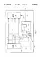
- FIG. 1is a block diagram of a preferred embodiment employing the principles of the present invention.
- FIG. 2is a timing diagram illustrating certain operations performed by the embodiment shown in FIG. 1.
- FIG. 3is a block diagram showing further details of the multiple-input signature module of FIG. 1.
- FIG. 4is a block diagram showing an alternative embodiment of the multiple-input signature module of FIG. 1.
- FIG. 5is a block diagram illustrating further details of FIGS. 3 and 4.
- FIG. 6is a block diagram showing a scan chain which includes the multiple-input signature module of FIG. 1.
- an integrated circuit chip 100includes a first circuit module 102 and a second circuit module 104.
- Circuit module 102preferably includes a plurality of digital circuits that generate data signals 106 and address and other control signals 108. Data signals 106 and address/control signals 108 are received by circuit module 104.
- Circuit modules 102 and 104may take a variety of forms to perform a variety of functions. For example, in a preferred embodiment circuit module 102 takes the form of a graphics controller that generates data signals 106 and address and control signals 108. Circuit module 104 in such an embodiment takes the form of a Dynamic Random Access Memory (DRAM) that stores data 106 at addresses indicated by address/control signals 108.
- DRAMDynamic Random Access Memory
- Data signals 106 and address/control signals 108are each received by a multiple input signature module 110, which operates in accordance with control signals generated by control module 112.
- Multiple input signature module 110advantageously operates in accordance with the principles of the present invention to capture data values transmitted via signals 106 and 108, to compress such data values, and to provide a signature value indicative of such data values to an output pin (or output structure) of chip 100 by way of signal line 114.
- the signature value provided by an equivalent multiple input signature module 110is provided in parallel to a plurality of pins on chip 100.
- Circuit module 102may also generate mask bits 324 which perform a function described in greater detail herein.
- Multiple input signature module 110includes a plurality of storage elements 116 (shown individually as 116.1, 116.2 . . . , 116.n). In an exemplary embodiment, multiple input signature module 110 includes 145 storage elements 116, corresponding to 128 data signals 106, and 17 address signals, part of address/control signals 108.
- Multiple input signature module 110preferably captures data values transmitted by way of signal lines 106 and 108 in a manner shown in the timing diagram of FIG. 2.
- Circuit modules 102 and 104are preferably synchronous circuits whose interaction (interfaces) operate in accordance with a clock signal 118.
- Data values 106 and address/control values 108are stored in multiple input signature module 110 and in circuit module 104 upon each rising edge of write enable signal 120.
- Data on signal lines 106is written to storage locations in circuit module 104 at addresses designated by address/control lines 108 in accordance with write enable signal 120.
- write enable signal 120causes data values on signal lines 106 to be written to circuit module 104 at locations specified by address values on address/control lines 108
- the same values indicated by data line 106 and address/control lines 108are stored to multiple input signature module 110 by virtue of write enable signal 120.
- Multiple input signature module 110advantageously operates to create a unique incremental signature value in response to the multiple data values stored to multiple input signature module 110 by way of write enable signal 120.
- FIG. 3illustrates further details of one stage of multiple input signature module 110.
- Each stage of multiple input signature module 110comprises a storage element 116 which in a preferred embodiment takes the form of a D-type flip-flop.
- signature generation circuitry 301Associated with each storage element is signature generation circuitry 301 and clock control circuitry 303.
- the signature generation circuitry 301generates a portion of the signature value for storage in the associated storage element 116.
- the clock control circuitry 303controls when data is stored to each storage element 116 of the module 110.
- Storage element 116preferably includes a scan input (SIN), and a scan enable input (SMC) in addition to a data input (D), data output (Q) 330, and a clock input (CLK), to allow the storage element 116 to form a portion of a scan chain. Details of scan chains are described in "Logic Design Principles" by E. J. McClusky, 1986, Prentice Hall, N.J. Assertion of the clock signal CLK causes data at the
- Clock inputis generated by way of logic elements 302, 304, and 306.
- CLK signal 118is provided to the CLK input when scan mode is enabled by way of scan-enable signal 308, or if multiple input signature module 110 is enabled by way of MISR ON signal 310 and write enable signal 120 is asserted.
- datais clocked into storage element 110 under control of CLK signal, either during scan mode or when the multiple input signature module is enabled and the write enable signal is asserted.
- Signature generation circuitry 301generates a portion of the signature value by way of XOR gate 314 which receives a masked present stage data bit 315, a prior stage data bit 320 and (for selected stages) a tap bit 322.
- Masked present stage data bit 315is derived from present stage data bit 318 which corresponds to one of the signal lines 106 or 108.
- Prior stage data bit 320corresponds to the output bit 330 of the previous stage.
- Storage element bits of module 110are connected in a shift register for scan purposes, bit 330 of a stage such as 116.1 connected to bit 320 of the next stage 116.2.
- Masked present stage data bit 315is generated by AND gate 312 which masks present stage data bit 318 when mask bit 324 is zero.
- Mask bit 324 and AND gate 312operate to force present stage data bit 318 to a zero value when the signal line 106 or 108 corresponding to bit 318 is not being driven by circuit module 102.
- circuit module 104is a DRAM
- certain write operations performed by circuit module 102may result in only some bits of data lines 106 being written to a location in circuit module 104. In such an instance, the data value on the signal lines 106 and 108 not being written to circuit module 104 may not be known.
- Mask bit 324 and AND gate 312advantageously operate to force a known present stage data value to be generated to XOR gate 314. The exact value, be it zero or one, is unimportant so long as it is predetermined and the signature value remains deterministic (predictable) and not affected by unknown ("x”) data.
- Mask bit 324is generated in a manner shown in further detail in FIG. 5.
- Register 502which in a preferred embodiment is contained in circuit module 102, contains a plurality of mask bits, with each mask bit corresponding to one or more bits of signal lines 106.
- register 502comprises 16 bits, with one mask bit of register 502 corresponding to a byte (8 bits) of signal lines 106.
- DRAM 104is byte addressable, to allow read and write operations to be performed on a byte basis. Therefore only one mask bit per byte is required.
- Mask bitsare stored in register 502 to generate mask bits 324.
- circuit module 102During any particular cycle when circuit module 102 is writing data to circuit module 104, it sets bits in register 502 corresponding to the bytes of data on signal lines 106 that are being written to circuit module 104.
- the other mask bitsare set to the masking value causing the corresponding present stage data bytes to be masked to a predetermined value.
- Tap bit 322corresponds to a selected stage output bit 330.
- signature module 110which comprises 145 stages, is implemented as five sub-modules of 29 stages each. The five sub-modules are interlinked by way of the scan logic described herein. If the stages are numbered sequentially from 0 to 144 then stages 0, 29, 58, 87 and 116 each receive 3 XORed tap bits. Specifically, stage zero receives tap bits 322 (XORed) that correspond to bit 330 of stages 0, 1 and 28. Stage 29 receives 3 tap bits, 330 that correspond to stages 29, 30 and 57. Stage 58 receives 3 tap bits 330 that correspond to stages 58, 59 and 86.
- Stage 87receives 3 tap bits 330 that correspond to bits 330 of stages 87, 88 and 115.
- Stage 116receives 3 tap bits 330 that corresponds to bits 116, 117 and 144.
- Principles of signature value generationare described in "Logic Design Principles" by E. J. McClusky 1986, Prentice Hall, N.J.
- NOR gate 316operates in response to DIAG-ON signal 317 to reset storage element 116.
- the exact manner in which the storage elements 116 are resetis unimportant so long as they are set to a known value.
- FIG. 4 of the drawingsshows an alternative embodiment in which storage elements are reset to a known value by way of a reset input over the storage elements.
- FIG. 4is the same in all other respects as FIG. 3, with the exception that XOR gate 314 is changed to an XNOR gate 414 to account for the inverting function provided by NOR gate 316. It is important that storage elements 116 be initialized to a known value to ensure the integrity of the signature value generated by signature module 110.
- the module 110may be used during a diagnostic mode to capture data at a single cycle, rather than capturing data over multiple cycles.
- the signature registeris initialized at the cycle previous to the cycle being diagnosed, then one cycle is run to capture data in the cycle under test, then scan is used to examine the data.
- the signature value generated and stored by the signature module 110is preferably provided to outputs of the chip 100 under control of scan enable 308 which causes the storage elements 116 of the signature module 110 to form a portion of a scan chain.
- An example of such a scan chainis shown in FIG. 6.
- a plurality of storage elements 602(shown individually 602.1, 602.2 . . . , 602.12) contained in circuit modules 102 and 104 are interlinked such that each storage element (typically a D-type flip-flop) receives a scan input which is the data output from another storage element. Included within the scan chain shown in FIG. 6 are the storage elements 116 of signature module 110.
- the scan enable signal 308causes signal 320 what is provided to the scan input (SIN) of the storage elements to be stored in the corresponding storage element.
- SINscan input
- each of the storage elementsare serially connected to form a portion of the scan chain of the chip 100.
- the signature valuecan then be provided as a portion of a scan output signal obtained at an appropriate scan out pin on the chip 100.
- the signature valuemay be provided to outputs of the chip 100 in parallel, either by use of dedicated pins or by multiplexing the signature value onto pins ordinarily used for another purpose.
Landscapes
- Engineering & Computer Science (AREA)
- General Engineering & Computer Science (AREA)
- Physics & Mathematics (AREA)
- General Physics & Mathematics (AREA)
- Tests Of Electronic Circuits (AREA)
- For Increasing The Reliability Of Semiconductor Memories (AREA)
Abstract
Description
Claims (14)
Priority Applications (1)
| Application Number | Priority Date | Filing Date | Title |
|---|---|---|---|
| US09/075,350US6158033A (en) | 1998-05-08 | 1998-05-08 | Multiple input signature testing & diagnosis for embedded blocks in integrated circuits |
Applications Claiming Priority (1)
| Application Number | Priority Date | Filing Date | Title |
|---|---|---|---|
| US09/075,350US6158033A (en) | 1998-05-08 | 1998-05-08 | Multiple input signature testing & diagnosis for embedded blocks in integrated circuits |
Publications (1)
| Publication Number | Publication Date |
|---|---|
| US6158033Atrue US6158033A (en) | 2000-12-05 |
Family
ID=22125129
Family Applications (1)
| Application Number | Title | Priority Date | Filing Date |
|---|---|---|---|
| US09/075,350Expired - LifetimeUS6158033A (en) | 1998-05-08 | 1998-05-08 | Multiple input signature testing & diagnosis for embedded blocks in integrated circuits |
Country Status (1)
| Country | Link |
|---|---|
| US (1) | US6158033A (en) |
Cited By (17)
| Publication number | Priority date | Publication date | Assignee | Title |
|---|---|---|---|---|
| US6442723B1 (en)* | 1999-05-12 | 2002-08-27 | International Business Machines Corporation | Logic built-in self test selective signature generation |
| WO2002063313A3 (en)* | 2001-02-02 | 2003-02-13 | Logicvision Inc | Method for scan testing of digital circuit, digital circuit and program product |
| US6536007B1 (en)* | 2000-06-30 | 2003-03-18 | Intel Corporation | Models and technique for automated fault isolation of open defects in logic |
| US6745359B2 (en) | 2002-06-06 | 2004-06-01 | Logicvision, Inc. | Method of masking corrupt bits during signature analysis and circuit for use therewith |
| US20040107395A1 (en)* | 2002-12-03 | 2004-06-03 | Volkerink Erik H. | System and method for testing circuitry using an externally generated signature |
| US20050222816A1 (en)* | 2004-03-31 | 2005-10-06 | Wu-Tung Cheng | Compactor independent fault diagnosis |
| US20050251708A1 (en)* | 2004-04-21 | 2005-11-10 | Stmicroelectronics Sa | Microprocessor comprising error detection means protected against an attack by error injection |
| US20060111873A1 (en)* | 2004-03-31 | 2006-05-25 | Yu Huang | Compactor independent direct diagnosis of test hardware |
| US7203878B2 (en)* | 2002-07-19 | 2007-04-10 | Sun Microsystems, Inc. | System and method for performing predictable signature analysis in the presence of multiple data streams |
| US20070100586A1 (en)* | 2004-03-31 | 2007-05-03 | Wu-Tung Cheng | Direct fault diagnostics using per-pattern compactor signatures |
| US20070115833A1 (en)* | 2005-11-21 | 2007-05-24 | Gerald Pepper | Varying the position of test information in data units |
| US20070257701A1 (en)* | 2006-02-15 | 2007-11-08 | Stmicroelectronics Sa | Integrated circuit comprising a test mode secured by the use of an identifier, and associated method |
| US7401280B1 (en)* | 2005-01-13 | 2008-07-15 | Lattice Semiconductor Corporation | Self-verification of configuration memory in programmable logic devices |
| US20080263421A1 (en)* | 2003-08-20 | 2008-10-23 | Michael Goessel | Electrical Diagnostic Circuit and Method for the Testing and/or the Diagnostic Analysis of an Integrated Circuit |
| US20090300249A1 (en)* | 2008-05-30 | 2009-12-03 | Moyer William C | Selective misr data accumulation during exception processing |
| US9305590B2 (en) | 2007-10-16 | 2016-04-05 | Seagate Technology Llc | Prevent data storage device circuitry swap |
| US9679602B2 (en) | 2006-06-14 | 2017-06-13 | Seagate Technology Llc | Disc drive circuitry swap |
Citations (4)
| Publication number | Priority date | Publication date | Assignee | Title |
|---|---|---|---|---|
| US4513418A (en)* | 1982-11-08 | 1985-04-23 | International Business Machines Corporation | Simultaneous self-testing system |
| US4519078A (en)* | 1982-09-29 | 1985-05-21 | Storage Technology Corporation | LSI self-test method |
| US5583786A (en)* | 1993-12-30 | 1996-12-10 | Intel Corporation | Apparatus and method for testing integrated circuits |
| US5983380A (en)* | 1997-09-16 | 1999-11-09 | International Business Machines Corporation | Weighted random pattern built-in self-test |
- 1998
- 1998-05-08USUS09/075,350patent/US6158033A/ennot_activeExpired - Lifetime
Patent Citations (4)
| Publication number | Priority date | Publication date | Assignee | Title |
|---|---|---|---|---|
| US4519078A (en)* | 1982-09-29 | 1985-05-21 | Storage Technology Corporation | LSI self-test method |
| US4513418A (en)* | 1982-11-08 | 1985-04-23 | International Business Machines Corporation | Simultaneous self-testing system |
| US5583786A (en)* | 1993-12-30 | 1996-12-10 | Intel Corporation | Apparatus and method for testing integrated circuits |
| US5983380A (en)* | 1997-09-16 | 1999-11-09 | International Business Machines Corporation | Weighted random pattern built-in self-test |
Non-Patent Citations (4)
| Title |
|---|
| Bernd Konemann, et al., "Built-In Test for Complex Digital Integrated Circuits", IEEE Journal of Solid State Circuits, vol. SC-15, No. 3, Jun. 1980. |
| Bernd Konemann, et al., Built In Test for Complex Digital Integrated Circuits , IEEE Journal of Solid State Circuits, vol. SC 15, No. 3, Jun. 1980.* |
| Edward J. McCluskey, "Logic Design Principles--With Emphasis on Testable Semicustom Circuits" 1986. |
| Edward J. McCluskey, Logic Design Principles With Emphasis on Testable Semicustom Circuits 1986.* |
Cited By (32)
| Publication number | Priority date | Publication date | Assignee | Title |
|---|---|---|---|---|
| US6442723B1 (en)* | 1999-05-12 | 2002-08-27 | International Business Machines Corporation | Logic built-in self test selective signature generation |
| US6536007B1 (en)* | 2000-06-30 | 2003-03-18 | Intel Corporation | Models and technique for automated fault isolation of open defects in logic |
| WO2002063313A3 (en)* | 2001-02-02 | 2003-02-13 | Logicvision Inc | Method for scan testing of digital circuit, digital circuit and program product |
| US6745359B2 (en) | 2002-06-06 | 2004-06-01 | Logicvision, Inc. | Method of masking corrupt bits during signature analysis and circuit for use therewith |
| US7203878B2 (en)* | 2002-07-19 | 2007-04-10 | Sun Microsystems, Inc. | System and method for performing predictable signature analysis in the presence of multiple data streams |
| US7131046B2 (en) | 2002-12-03 | 2006-10-31 | Verigy Ipco | System and method for testing circuitry using an externally generated signature |
| US20040107395A1 (en)* | 2002-12-03 | 2004-06-03 | Volkerink Erik H. | System and method for testing circuitry using an externally generated signature |
| US20080263421A1 (en)* | 2003-08-20 | 2008-10-23 | Michael Goessel | Electrical Diagnostic Circuit and Method for the Testing and/or the Diagnostic Analysis of an Integrated Circuit |
| US7814384B2 (en) | 2003-08-20 | 2010-10-12 | Infineon Technologies Ag | Electrical diagnostic circuit and method for the testing and/or the diagnostic analysis of an integrated circuit |
| US20060111873A1 (en)* | 2004-03-31 | 2006-05-25 | Yu Huang | Compactor independent direct diagnosis of test hardware |
| US8280688B2 (en) | 2004-03-31 | 2012-10-02 | Mentor Graphics Corporation | Compactor independent direct diagnosis of test hardware |
| US20070100586A1 (en)* | 2004-03-31 | 2007-05-03 | Wu-Tung Cheng | Direct fault diagnostics using per-pattern compactor signatures |
| US8280687B2 (en) | 2004-03-31 | 2012-10-02 | Mentor Graphics Corporation | Direct fault diagnostics using per-pattern compactor signatures |
| US7239978B2 (en) | 2004-03-31 | 2007-07-03 | Wu-Tung Cheng | Compactor independent fault diagnosis |
| US8301414B2 (en) | 2004-03-31 | 2012-10-30 | Mentor Graphics Corporation | Compactor independent fault diagnosis |
| US20070283202A1 (en)* | 2004-03-31 | 2007-12-06 | Wu-Tung Cheng | Compactor independent fault diagnosis |
| US20100306606A1 (en)* | 2004-03-31 | 2010-12-02 | Yu Huang | Compactor independent direct diagnosis of test hardware |
| US20050222816A1 (en)* | 2004-03-31 | 2005-10-06 | Wu-Tung Cheng | Compactor independent fault diagnosis |
| US7729884B2 (en) | 2004-03-31 | 2010-06-01 | Yu Huang | Compactor independent direct diagnosis of test hardware |
| US8341475B2 (en) | 2004-04-21 | 2012-12-25 | Stmicroelectronics Sa | Microprocessor comprising signature means for detecting an attack by error injection |
| US7584386B2 (en)* | 2004-04-21 | 2009-09-01 | Stmicroelectronics Sa | Microprocessor comprising error detection means protected against an attack by error injection |
| US20050268163A1 (en)* | 2004-04-21 | 2005-12-01 | Stmicroelectronics Sa | Microprocessor comprising signature means for detecting an attack by error injection |
| US20050251708A1 (en)* | 2004-04-21 | 2005-11-10 | Stmicroelectronics Sa | Microprocessor comprising error detection means protected against an attack by error injection |
| US7904775B2 (en)* | 2004-04-21 | 2011-03-08 | Stmicroelectronics Sa | Microprocessor comprising signature means for detecting an attack by error injection |
| US7401280B1 (en)* | 2005-01-13 | 2008-07-15 | Lattice Semiconductor Corporation | Self-verification of configuration memory in programmable logic devices |
| US20070115833A1 (en)* | 2005-11-21 | 2007-05-24 | Gerald Pepper | Varying the position of test information in data units |
| US7921342B2 (en)* | 2006-02-15 | 2011-04-05 | Stmicroelectronics Sa | Integrated circuit comprising a test mode secured by the use of an identifier, and associated method |
| US20070257701A1 (en)* | 2006-02-15 | 2007-11-08 | Stmicroelectronics Sa | Integrated circuit comprising a test mode secured by the use of an identifier, and associated method |
| US9679602B2 (en) | 2006-06-14 | 2017-06-13 | Seagate Technology Llc | Disc drive circuitry swap |
| US9305590B2 (en) | 2007-10-16 | 2016-04-05 | Seagate Technology Llc | Prevent data storage device circuitry swap |
| US8060730B2 (en)* | 2008-05-30 | 2011-11-15 | Freescale Semiconductor, Inc. | Selective MISR data accumulation during exception processing |
| US20090300249A1 (en)* | 2008-05-30 | 2009-12-03 | Moyer William C | Selective misr data accumulation during exception processing |
Similar Documents
| Publication | Publication Date | Title |
|---|---|---|
| US6158033A (en) | Multiple input signature testing & diagnosis for embedded blocks in integrated circuits | |
| US6671839B1 (en) | Scan test method for providing real time identification of failing test patterns and test bist controller for use therewith | |
| US6668347B1 (en) | Built-in self-testing for embedded memory | |
| US6510398B1 (en) | Constrained signature-based test | |
| US4974184A (en) | Maximum length pseudo-random test pattern generator via feedback network modification | |
| US6122762A (en) | Memory interface device and method for supporting debugging | |
| US5825785A (en) | Serial input shift register built-in self test circuit for embedded circuits | |
| US6510534B1 (en) | Method and apparatus for testing high performance circuits | |
| US6658611B1 (en) | Programmable built-in self-test system for semiconductor memory device | |
| US7137086B2 (en) | Assertion checking using two or more cores | |
| US6553530B1 (en) | Integrated circuit devices that include self-test apparatus for testing a plurality of functional blocks and methods of testing same | |
| US6934900B1 (en) | Test pattern generator for SRAM and DRAM | |
| KR960042082A (en) | Embedded logic circuit inspection system and its inspection method and integrated circuit chip | |
| JP3645578B2 (en) | Apparatus and method for embedded self-test of smart memory | |
| JP2003332443A (en) | Semiconductor integrated circuit, design support apparatus therefor, and test method | |
| JPH05241882A (en) | Built-in self testing circuit and method for executing self test | |
| US20100218059A1 (en) | On-Chip Seed Generation Using Boolean Functions for LFSR Re-Seeding Based Logic BIST Techniques for Low Cost Field Testability | |
| KR19980064254A (en) | Integrated circuit memory device with built-in self test circuit with monitor and tester mode | |
| US12105145B2 (en) | Scan compression through pin data encoding | |
| US7096397B2 (en) | Dft technique for avoiding contention/conflict in logic built-in self-test | |
| US6789220B1 (en) | Method and apparatus for vector processing | |
| US7028239B2 (en) | Microprocessor on-chip testing architecture and implementation | |
| US9329232B2 (en) | Scan response reuse method and apparatus | |
| GB2420421A (en) | Method and apparatus for an embedded time domain reflectometry test | |
| EP1647828B1 (en) | Automatic fault-testing of logic blocks using internal at-speed logic-BIST |
Legal Events
| Date | Code | Title | Description |
|---|---|---|---|
| AS | Assignment | Owner name:S3 INCORPORATED, CALIFORNIA Free format text:ASSIGNMENT OF ASSIGNORS INTEREST;ASSIGNORS:WAGNER, KENNETH D.;AMERIAN, MEHRAN;REEL/FRAME:009162/0154 Effective date:19980507 | |
| STCF | Information on status: patent grant | Free format text:PATENTED CASE | |
| AS | Assignment | Owner name:SONICBLUE INCORPORATED, CALIFORNIA Free format text:CHANGE OF NAME;ASSIGNOR:S3 INCORPORATED;REEL/FRAME:011837/0642 Effective date:20001109 | |
| AS | Assignment | Owner name:TREPTON RESEARCH GROUP, CALIFORNIA Free format text:ASSIGNMENT OF ASSIGNORS INTEREST;ASSIGNORS:BINAR GRAPHICS, INC.;DIAMOND MEDIA SYSTEMS, INC.;FRONT PATH, INC.;AND OTHERS;REEL/FRAME:014646/0812 Effective date:20031009 | |
| AS | Assignment | Owner name:TREPTON RESEARCH GROUP, INC., CALIFORNIA Free format text:ASSIGNMENT OF ASSIGNORS INTEREST;ASSIGNOR:SONICBLUE INCORPORATED;REEL/FRAME:014532/0711 Effective date:20031009 | |
| FPAY | Fee payment | Year of fee payment:4 | |
| AS | Assignment | Owner name:ALTERA CORPORATION, CALIFORNIA Free format text:ASSIGNMENT OF ASSIGNORS INTEREST;ASSIGNOR:TREPTON RESEARCH GROUP;REEL/FRAME:019140/0818 Effective date:20070307 | |
| FPAY | Fee payment | Year of fee payment:8 | |
| FPAY | Fee payment | Year of fee payment:12 |