US6157356A - Digitally driven gray scale operation of active matrix OLED displays - Google Patents
Digitally driven gray scale operation of active matrix OLED displaysDownload PDFInfo
- Publication number
- US6157356A US6157356AUS08/631,350US63135096AUS6157356AUS 6157356 AUS6157356 AUS 6157356AUS 63135096 AUS63135096 AUS 63135096AUS 6157356 AUS6157356 AUS 6157356A
- Authority
- US
- United States
- Prior art keywords
- pixel circuit
- channel
- oled
- fabricated
- control device
- Prior art date
- Legal status (The legal status is an assumption and is not a legal conclusion. Google has not performed a legal analysis and makes no representation as to the accuracy of the status listed.)
- Expired - Lifetime
Links
Images


Classifications
- G—PHYSICS
- G09—EDUCATION; CRYPTOGRAPHY; DISPLAY; ADVERTISING; SEALS
- G09G—ARRANGEMENTS OR CIRCUITS FOR CONTROL OF INDICATING DEVICES USING STATIC MEANS TO PRESENT VARIABLE INFORMATION
- G09G3/00—Control arrangements or circuits, of interest only in connection with visual indicators other than cathode-ray tubes
- G09G3/20—Control arrangements or circuits, of interest only in connection with visual indicators other than cathode-ray tubes for presentation of an assembly of a number of characters, e.g. a page, by composing the assembly by combination of individual elements arranged in a matrix no fixed position being assigned to or needed to be assigned to the individual characters or partial characters
- G09G3/22—Control arrangements or circuits, of interest only in connection with visual indicators other than cathode-ray tubes for presentation of an assembly of a number of characters, e.g. a page, by composing the assembly by combination of individual elements arranged in a matrix no fixed position being assigned to or needed to be assigned to the individual characters or partial characters using controlled light sources
- G09G3/30—Control arrangements or circuits, of interest only in connection with visual indicators other than cathode-ray tubes for presentation of an assembly of a number of characters, e.g. a page, by composing the assembly by combination of individual elements arranged in a matrix no fixed position being assigned to or needed to be assigned to the individual characters or partial characters using controlled light sources using electroluminescent panels
- G09G3/32—Control arrangements or circuits, of interest only in connection with visual indicators other than cathode-ray tubes for presentation of an assembly of a number of characters, e.g. a page, by composing the assembly by combination of individual elements arranged in a matrix no fixed position being assigned to or needed to be assigned to the individual characters or partial characters using controlled light sources using electroluminescent panels semiconductive, e.g. using light-emitting diodes [LED]
- G09G3/3208—Control arrangements or circuits, of interest only in connection with visual indicators other than cathode-ray tubes for presentation of an assembly of a number of characters, e.g. a page, by composing the assembly by combination of individual elements arranged in a matrix no fixed position being assigned to or needed to be assigned to the individual characters or partial characters using controlled light sources using electroluminescent panels semiconductive, e.g. using light-emitting diodes [LED] organic, e.g. using organic light-emitting diodes [OLED]
- G09G3/3225—Control arrangements or circuits, of interest only in connection with visual indicators other than cathode-ray tubes for presentation of an assembly of a number of characters, e.g. a page, by composing the assembly by combination of individual elements arranged in a matrix no fixed position being assigned to or needed to be assigned to the individual characters or partial characters using controlled light sources using electroluminescent panels semiconductive, e.g. using light-emitting diodes [LED] organic, e.g. using organic light-emitting diodes [OLED] using an active matrix
- G09G3/3233—Control arrangements or circuits, of interest only in connection with visual indicators other than cathode-ray tubes for presentation of an assembly of a number of characters, e.g. a page, by composing the assembly by combination of individual elements arranged in a matrix no fixed position being assigned to or needed to be assigned to the individual characters or partial characters using controlled light sources using electroluminescent panels semiconductive, e.g. using light-emitting diodes [LED] organic, e.g. using organic light-emitting diodes [OLED] using an active matrix with pixel circuitry controlling the current through the light-emitting element
- G—PHYSICS
- G09—EDUCATION; CRYPTOGRAPHY; DISPLAY; ADVERTISING; SEALS
- G09G—ARRANGEMENTS OR CIRCUITS FOR CONTROL OF INDICATING DEVICES USING STATIC MEANS TO PRESENT VARIABLE INFORMATION
- G09G3/00—Control arrangements or circuits, of interest only in connection with visual indicators other than cathode-ray tubes
- G09G3/20—Control arrangements or circuits, of interest only in connection with visual indicators other than cathode-ray tubes for presentation of an assembly of a number of characters, e.g. a page, by composing the assembly by combination of individual elements arranged in a matrix no fixed position being assigned to or needed to be assigned to the individual characters or partial characters
- G09G3/2007—Display of intermediate tones
- G09G3/2018—Display of intermediate tones by time modulation using two or more time intervals
- G09G3/2022—Display of intermediate tones by time modulation using two or more time intervals using sub-frames
- G—PHYSICS
- G09—EDUCATION; CRYPTOGRAPHY; DISPLAY; ADVERTISING; SEALS
- G09G—ARRANGEMENTS OR CIRCUITS FOR CONTROL OF INDICATING DEVICES USING STATIC MEANS TO PRESENT VARIABLE INFORMATION
- G09G2300/00—Aspects of the constitution of display devices
- G09G2300/08—Active matrix structure, i.e. with use of active elements, inclusive of non-linear two terminal elements, in the pixels together with light emitting or modulating elements
- G09G2300/0809—Several active elements per pixel in active matrix panels
- G09G2300/0842—Several active elements per pixel in active matrix panels forming a memory circuit, e.g. a dynamic memory with one capacitor
Definitions
- the inventionrelates to a pixel circuit that enables gray scale operation of an active matrix display using organic light emitting diodes.
- references (1,2,3)teach the layout and related fabrication steps for a passive matrix OLED display.
- the pixelmust emit 480 times as much light as a pixel that emits constantly.
- the disadvantages of such operationare (a) higher voltage with attendant higher power, (b) operation at sub-optimum levels of electrical/optical conversion efficiency, (c) possible visual artifacts, and (d) faster degradation of the display.
- An active matrix OLED displaywould solve these problems.
- Reference (4)teaches a pixel circuit designed for gray scale operation in an active matrix OLED display.
- This circuitstores the n bits of gray scale in n memory elements at each pixel.
- this circuitrequires at least 6n+2 MOS transistors and n column lines, per pixel. Such a circuit would be much too large for use in a practical display. What is needed is a much simpler circuit.
- This disclosureteaches a simple pixel circuit for achieving active matrix operation in an OLED display. It also teaches how such a pixel circuit can be digitally driven to achieve gray-scale operation of the display.
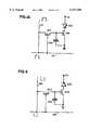
- FIG. 1Ais the preferred embodiment of the pixel circuit.
- the access device 102 and the current control device 106are both N-channel MOSFETs or TFTs, and the OLED 108 is in the common anode configuration.
- FIG. 1Bis a two-dimensional array of the pixel circuit showing how the active matrix OLED display is formed.
- FIG. 2shows a simplified cross section when the pixel circuit is implemented on a silicon substrate.
- the access device and the current control devicesare MOSFETs.
- FIG. 3shows the relevant cross section when the pixel circuit is implemented on a glass substrate.
- the access device and the current control devicesare either amorphous or polycrystalline silicon TFTs.
- FIG. 4is an alternative embodiment of the pixel circuit in which access device 402 and current control device 406 are both P-channel MOSFETs or TFTs, and the OLED 408 is in the common cathode configuration.
- FIG. 5is an alternative embodiment of the pixel circuit in which the access device 502 is an N-channel MOSFET or TFT and the current control device 506 is a P-channel MOSFET or TFT.
- the OLED 508is in the common cathode configuration.
- FIG. 6is an alternative embodiment of the pixel circuit in which the access device 602 is an P-channel MOSFET or TFT and the current control device 606 is a N-channel MOSFET or TFT.
- the OLED 608is in the common anode configuration.
- FIG. 1Ashows the preferred embodiment of the pixel circuit.
- the access device 102is used to place a voltage on capacitor 104. If this voltage exceeds the threshold voltage of device 106, both it and the organic light-emitting diode (OLED) 108 conduct current, and light is emitted from OLED 108.
- devices 102 and 106are N-channel metal-oxide-semiconductor field-effect transistors (MOSFETs) or N-channel thin-film transistors (TFTs), and OLED 108 has a common anode configuration.
- the bias voltage V bis applied to all diodes in the display.
- An active matrix displayis created by building a two-dimensional array of pixels using the two transistor pixel circuit shown in FIG. 1A. The result is indicated by the 3 ⁇ 3 array shown in FIG. 1B.
- a particular pixelis addressed by choosing the row line 110b and the column line 112b. When the row line is activated, transistor 102 is turned on, and the voltage on column line 112b is transferred to the capacitor 104. When the row line is de-activated, the voltage is held on capacitor 104 until the same row line is again activated.
- the pixels along an entire row line 110bare written at one time by placing the appropriate voltage on all of the column lines in the array (112a, 112b, 112c, etc.) during a line time.
- the pixel circuit of FIG. 1can be implemented in many ways.
- the access transistor and current control transistorare MOSFETs fabricated according to well known techniques practiced in the integrated circuit industry.
- the relevant cross sectionis shown in FIG. 2.
- the diffusion 204is formed in a silicon substrate of the opposite type (202).
- An insulating film 206is formed over the substrate and a contact hole is etched through the insulating film, permitting contact of the metal film 208 with the diffusion.
- This metal filmis etched into patterns, forming one electrode of the OLEDs.
- the organic films 210are thermally evaporated as discussed in references (5,6).
- transparent conductive film 212(such as ITO) is deposited to form the common electrode.
- the access transistor and current control transistorare amorphous or polycrystalline thin-film transistors fabricated according to well known techniques practiced in the display industry for active matrix liquid-crystal displays.
- FIG. 3shows a relevant cross section.
- a highly conductive polycrystalline region 304is formed on a glass substrate 302.
- an insulating layer 306is formed and a contact hole etched, allowing the metal film 308 to contact region 304.
- the organic film layers 310are thermally evaporated as discussed in references (5,6).
- the transparent conductive film 312is deposited to form the common electrode.
- Gray-scale operation of the displayis accomplished by dividing the frame time T f into multiple sub-frames T sfk and addressing all row lines during each sub-frame time.
- Each column lineis either V h or V l during the line time, and this voltage is written into the storage capacitor 104 of all pixels along the activated row line.
- V his chosen sufficiently greater than V t so that the ON impedance of transistor 106 is negligible compared to the diode impedance.
- n bits of gray scalethere are n sub-frames, and the sum of all sub-frame times equals the frame time T f .
- a pixel's luminanceis proportional to the sub-frame time, and each of the sub-frame times is weighted to produce the 2 n gray scale levels.
- Various weightingsare possible and a binary weighting algorithm is discussed below.
- each sub-framerequires M ⁇ N bits of data, and these are stored in a buffer memory.
- N bitsare read from the buffer memory and written to the N storage capacitors on the accessed row line, and this is continued until all row lines have been accessed.
- the time required to transfer all M ⁇ N bitsis the write time T w , and this time must be less than the sub-frame time for the least significant bit. Under this condition the length of time a signal is stored is equal to the sub-frame time for every pixel in the display.
- n bitsto a pixel.
- the weightingsare 1/15, 2/15, 4/15, and 8/15.
- Another possible orderingis to present the most significant bit first, followed by the second-most significant bit, etc., until the least significant bit is reached. Still other orderings are possible, in which the bit ordering is chosen to avoid visual artifacts if they exist.
- n buffer memoriesare required. After the data from one buffer is transferred to the display, new data can be entered into that buffer as preparation for the next data transfer to the display, insuring continuous flow of data to the display without any dead time. This can also be accomplished by a single buffer memory having simultaneous read/write capability.
- FIG. 1Ashows a pixel circuit using two N-channel MOSFETs or TFTs for the access and current control transistors and a common anode OLED.
- the complementary circuit in FIG. 4can be used with a common cathode OLED 408.
- the access and control transistorsboth are P-channel FETs or TFTs, and the row and column lines operate with negative polarity pulses.
- the bias voltage V bis also negative.
- FIG. 5Another alternative for the common cathode OLED is shown in FIG. 5.
- This embodimentretains an N-channel MOSFET for the access transistor and a positive polarity for the row and column pulses. Now the roles of the V h and V l pulses are reversed i.e., the OLED 508 emits light when V l is stored on capacitor 504 and is dark when V h ⁇ V b is stored on capacitor 504.
- the fourth embodiment, shown in FIG. 6,is the complementary circuit to that shown in FIG. 5.
- the row and column pulsesare of negatively polarity, as is the bias voltage.
- the access transistoris a P-channel MOSFET or TFT and the current control transistor is an N-channel MOSFET or TFT.
Landscapes
- Engineering & Computer Science (AREA)
- Physics & Mathematics (AREA)
- Computer Hardware Design (AREA)
- General Physics & Mathematics (AREA)
- Theoretical Computer Science (AREA)
- Control Of Indicators Other Than Cathode Ray Tubes (AREA)
- Electroluminescent Light Sources (AREA)
Abstract
Description
Claims (20)
Priority Applications (1)
| Application Number | Priority Date | Filing Date | Title |
|---|---|---|---|
| US08/631,350US6157356A (en) | 1996-04-12 | 1996-04-12 | Digitally driven gray scale operation of active matrix OLED displays |
Applications Claiming Priority (1)
| Application Number | Priority Date | Filing Date | Title |
|---|---|---|---|
| US08/631,350US6157356A (en) | 1996-04-12 | 1996-04-12 | Digitally driven gray scale operation of active matrix OLED displays |
Publications (1)
| Publication Number | Publication Date |
|---|---|
| US6157356Atrue US6157356A (en) | 2000-12-05 |
Family
ID=24530826
Family Applications (1)
| Application Number | Title | Priority Date | Filing Date |
|---|---|---|---|
| US08/631,350Expired - LifetimeUS6157356A (en) | 1996-04-12 | 1996-04-12 | Digitally driven gray scale operation of active matrix OLED displays |
Country Status (1)
| Country | Link |
|---|---|
| US (1) | US6157356A (en) |
Cited By (74)
| Publication number | Priority date | Publication date | Assignee | Title |
|---|---|---|---|---|
| US20020039087A1 (en)* | 2000-10-02 | 2002-04-04 | Semiconductor Energy Laboratory Co., Ltd. | Self light emitting device and driving method thereof |
| US20020047852A1 (en)* | 2000-09-04 | 2002-04-25 | Kazutaka Inukai | Method of driving EL display device |
| US6384804B1 (en)* | 1998-11-25 | 2002-05-07 | Lucent Techonologies Inc. | Display comprising organic smart pixels |
| US20020093472A1 (en)* | 2001-01-18 | 2002-07-18 | Takaji Numao | Display, portable device, and substrate |
| US6429601B1 (en)* | 1998-02-18 | 2002-08-06 | Cambridge Display Technology Ltd. | Electroluminescent devices |
| US20020145582A1 (en)* | 2000-08-31 | 2002-10-10 | Shunpei Yamazaki | Display device and manufacturing method thereof |
| US20020196213A1 (en)* | 2001-06-21 | 2002-12-26 | Hajime Akimoto | Image display |
| US6504742B1 (en)* | 2001-10-31 | 2003-01-07 | Hewlett-Packard Company | 3-D memory device for large storage capacity |
| US20030025656A1 (en)* | 2001-08-03 | 2003-02-06 | Semiconductor Energy Laboratory Co., Ltd. | Display device and method of driving thereof |
| US20030058195A1 (en)* | 2000-01-14 | 2003-03-27 | Katsumi Adachi | Active matrix display device and method of driving the same |
| WO2003037040A1 (en)* | 2001-09-28 | 2003-05-01 | Samsung Electronics Co., Ltd. | Organic electroluminescence display panel and display apparatus using thereof |
| US20030095087A1 (en)* | 2001-11-20 | 2003-05-22 | International Business Machines Corporation | Data voltage current drive amoled pixel circuit |
| US20030137503A1 (en)* | 2002-01-24 | 2003-07-24 | Hajime Kimura | Semiconductor device and method of driving the semiconductor device |
| US6618030B2 (en)* | 1997-09-29 | 2003-09-09 | Sarnoff Corporation | Active matrix light emitting diode pixel structure and concomitant method |
| US6653750B2 (en)* | 1998-11-27 | 2003-11-25 | Sanyo Electric Co., Ltd. | Electroluminescence display apparatus for displaying gray scales |
| US20040012550A1 (en)* | 2000-07-27 | 2004-01-22 | Semiconductor Energy Laboratory Co., Ltd. | Method of driving display device |
| EP1391869A2 (en) | 2002-08-23 | 2004-02-25 | Samsung SDI Co., Ltd. | Circuit for driving matrix display panel with photoluminescence quenching devices and matrix display apparatus incorporating the circuit |
| US20040046715A1 (en)* | 2002-08-23 | 2004-03-11 | Samsung Sdi Co., Ltd. | Circuit for driving matrix display panel with photoluminescence quenching devices, and matrix display apparatus incorporating the circuit |
| US20040047143A1 (en)* | 2001-11-27 | 2004-03-11 | Junichi Maruyama | Drive circuit for organic el device |
| US20040070558A1 (en)* | 2000-05-24 | 2004-04-15 | Eastman Kodak Company | OLED display with aging compensation |
| US20040125055A1 (en)* | 2002-12-25 | 2004-07-01 | Chih-Feng Sung | [organic light emitting display] |
| DE10305870A1 (en)* | 2003-02-13 | 2004-08-26 | BÄR, Hans | Digital controllable matrix element for preparation of light emitting diodes (LED) useful in pixel electronics, and in electronic image representation based on polymers, silicon, or organic LED |
| US20040173811A1 (en)* | 2000-05-22 | 2004-09-09 | Semiconductor Energy Laboratory Co., Ltd, A Japan Corporation | Light emitting device and electrical appliance |
| US20040174349A1 (en)* | 2003-03-04 | 2004-09-09 | Libsch Frank Robert | Driving circuits for displays |
| US20040188685A1 (en)* | 2003-03-31 | 2004-09-30 | Industrial Technology Research Institute | Thin film transistor and fabrication method thereof |
| US6809710B2 (en)* | 2000-01-21 | 2004-10-26 | Emagin Corporation | Gray scale pixel driver for electronic display and method of operation therefor |
| US20040227704A1 (en)* | 2003-05-14 | 2004-11-18 | Wen-Chun Wang | Apparatus for improving yields and uniformity of active matrix oled panels |
| US6828725B2 (en)* | 2001-01-30 | 2004-12-07 | Semiconductor Energy Laboratory Co., Ltd. | Light emitting device |
| US20040252088A1 (en)* | 2003-06-16 | 2004-12-16 | Genshiro Kawachi | Organic EL light emitting display device |
| US20040263062A1 (en)* | 2003-06-30 | 2004-12-30 | Semiconductor Energy Laboratory Co., Ltd. | Light emitting device |
| US6858989B2 (en)* | 2001-09-20 | 2005-02-22 | Emagin Corporation | Method and system for stabilizing thin film transistors in AMOLED displays |
| US20050093801A1 (en)* | 2001-07-12 | 2005-05-05 | Semiconductor Energy Laboratory Co., Ltd. | Display device using electron source elements and method of driving same |
| US20050162416A1 (en)* | 2001-05-21 | 2005-07-28 | Chi Mei Optoelectronics Corp. | Method of display by sub-frame driving |
| US20050212740A1 (en)* | 2004-03-26 | 2005-09-29 | Semiconductor Energy Laboratory Co., Ltd. | Display device, driving method thereof, and electronic apparatus using the same |
| US20050259089A1 (en)* | 2002-05-16 | 2005-11-24 | Shunpei Yamazaki | Driving method of light emitting device |
| US6972746B1 (en)* | 1994-10-31 | 2005-12-06 | Semiconductor Energy Laboratory Co., Ltd. | Active matrix type flat-panel display device |
| US20060028407A1 (en)* | 2004-08-06 | 2006-02-09 | Chen-Jean Chou | Light emitting device display circuit and drive method thereof |
| US20060038762A1 (en)* | 2004-08-21 | 2006-02-23 | Chen-Jean Chou | Light emitting device display circuit and drive method thereof |
| US20060050040A1 (en)* | 2004-09-03 | 2006-03-09 | Chen-Jean Chou | Active Matrix Light Emitting Device Display and Drive Method Thereof |
| US20060066527A1 (en)* | 2004-09-24 | 2006-03-30 | Chen-Jean Chou | Active matrix light emitting device display pixel circuit and drive method |
| US20060071887A1 (en)* | 2004-10-01 | 2006-04-06 | Chen-Jean Chou | Active matrix display and drive method thereof |
| US20060119554A1 (en)* | 2004-12-06 | 2006-06-08 | Semiconductor Energy Laboratory Co., Ltd. | Display device, driving method thereof and electronic appliance |
| US20060139265A1 (en)* | 2004-12-28 | 2006-06-29 | Semiconductor Energy Laboratory Co., Ltd. | Driving method of display device |
| US20060232600A1 (en)* | 2005-04-14 | 2006-10-19 | Semiconductor Energy Laboratory Co., Ltd. | Display device, driving method of the display device, and electronic device |
| EP1231593A3 (en)* | 2001-02-08 | 2007-02-21 | Sanyo Electric Co. Ltd | Organic EL circuit |
| US20070171241A1 (en)* | 2006-01-20 | 2007-07-26 | Semiconductor Energy Laboratory Co., Ltd. | Driving method of display device |
| US7253815B2 (en) | 2003-06-05 | 2007-08-07 | Au Optronics Corp. | OLED display and pixel structure thereof |
| US20070273629A1 (en)* | 2006-05-23 | 2007-11-29 | Bily Wang | Display drive circuit and drive method for the same |
| US20070278932A1 (en)* | 2000-10-27 | 2007-12-06 | Semiconductor Energy Laboratory Co., Ltd. | Display Device and Method of Driving the Same |
| US20070290196A1 (en)* | 2005-07-08 | 2007-12-20 | Samsung Sdi Co., Ltd. | Organic light emitting display device and method for manufacturing the organic light emitting display device |
| CN100362563C (en)* | 2002-01-31 | 2008-01-16 | 株式会社东芝 | flat panel display device |
| US20080055223A1 (en)* | 2006-06-16 | 2008-03-06 | Roger Stewart | Pixel circuits and methods for driving pixels |
| US20080062091A1 (en)* | 2006-06-16 | 2008-03-13 | Roger Stewart | Pixel circuits and methods for driving pixels |
| US20080062090A1 (en)* | 2006-06-16 | 2008-03-13 | Roger Stewart | Pixel circuits and methods for driving pixels |
| US20080074358A1 (en)* | 2006-09-21 | 2008-03-27 | Sanyo Electric Co., Ltd. | Electroluminescence display apparatus and method of correcting display variation for electroluminescence display apparatus |
| CN100380433C (en)* | 2001-06-22 | 2008-04-09 | 统宝光电股份有限公司 | OLED current-driven pixel circuit |
| US20080100541A1 (en)* | 2006-11-01 | 2008-05-01 | Himax Technologies Limited | Organic light emitting diode pixel circuit |
| US20080179596A1 (en)* | 2007-01-26 | 2008-07-31 | Kyu-Sik Cho | Thin film transistor, organic light emitting device including thin film transistor, and manufacturing method thereof |
| US20090058772A1 (en)* | 2007-09-04 | 2009-03-05 | Samsung Electronics Co., Ltd. | Organic light emitting display and method for driving the same |
| US7623091B2 (en) | 2005-05-02 | 2009-11-24 | Semiconductor Energy Laboratory Co., Ltd. | Display device, and driving method and electronic apparatus of the display device |
| US7719526B2 (en) | 2005-04-14 | 2010-05-18 | Semiconductor Energy Laboratory Co., Ltd. | Display device, and driving method and electronic apparatus of the display device |
| US20110096239A1 (en)* | 2005-11-30 | 2011-04-28 | Microemissive Displays Limited | Temporary Memory Circuits for Matrix Display Device |
| US20110193885A1 (en)* | 2010-02-08 | 2011-08-11 | Samsung Electro-Mechanics Co., Ltd. | Organic light emitting display |
| CN101131958B (en)* | 2006-08-25 | 2011-08-24 | 中华映管股份有限公司 | Method for manufacturing pixel structure of organic electroluminescence display |
| WO2012032282A1 (en) | 2010-09-09 | 2012-03-15 | Cambridge Display Technology Limited | Organic light emitting diode displays |
| US20120299902A1 (en)* | 1997-02-17 | 2012-11-29 | Seiko Epson Corporation | Display apparatus |
| US8378935B2 (en) | 2005-01-14 | 2013-02-19 | Semiconductor Energy Laboratory Co., Ltd. | Display device having a plurality of subframes and method of driving the same |
| US8633878B2 (en) | 2001-06-21 | 2014-01-21 | Japan Display Inc. | Image display |
| US8743160B2 (en)* | 2011-12-01 | 2014-06-03 | Chihao Xu | Active matrix organic light-emitting diode display and method for driving the same |
| US9135853B2 (en) | 2012-04-13 | 2015-09-15 | Samsung Electronics Co., Ltd. | Gradation voltage generator and display driving apparatus |
| WO2015149398A1 (en)* | 2014-04-03 | 2015-10-08 | 深圳市华星光电技术有限公司 | Array substrate of oled display |
| US9307611B2 (en) | 2012-05-18 | 2016-04-05 | Semiconductor Energy Laboratory Co., Ltd. | Pixel circuit, display device, and electronic device |
| CN105489158A (en)* | 2014-09-19 | 2016-04-13 | 深圳Tcl新技术有限公司 | OLED (organic LED) pixel drive circuit and television set |
| WO2018167835A1 (en)* | 2017-03-14 | 2018-09-20 | シャープ株式会社 | Organic electroluminescence display device |
Citations (10)
| Publication number | Priority date | Publication date | Assignee | Title |
|---|---|---|---|---|
| US4621260A (en)* | 1982-12-25 | 1986-11-04 | Tokyo Shibaura Denki Kabushiki Kaisha | Thin-film transistor circuit |
| US4996523A (en)* | 1988-10-20 | 1991-02-26 | Eastman Kodak Company | Electroluminescent storage display with improved intensity driver circuits |
| US5276380A (en)* | 1991-12-30 | 1994-01-04 | Eastman Kodak Company | Organic electroluminescent image display device |
| US5294870A (en)* | 1991-12-30 | 1994-03-15 | Eastman Kodak Company | Organic electroluminescent multicolor image display device |
| US5294869A (en)* | 1991-12-30 | 1994-03-15 | Eastman Kodak Company | Organic electroluminescent multicolor image display device |
| US5349366A (en)* | 1991-10-29 | 1994-09-20 | Semiconductor Energy Laboratory Co., Ltd. | Electro-optical device and process for fabricating the same and method of driving the same |
| US5648792A (en)* | 1994-03-14 | 1997-07-15 | Hitachi, Ltd. | Liquid crystal display device having a thin film |
| US5748160A (en)* | 1995-08-21 | 1998-05-05 | Mororola, Inc. | Active driven LED matrices |
| US5751261A (en)* | 1990-12-31 | 1998-05-12 | Kopin Corporation | Control system for display panels |
| US5867138A (en)* | 1995-03-13 | 1999-02-02 | Samsung Electronics Co., Ltd. | Device for driving a thin film transistor liquid crystal display |
- 1996
- 1996-04-12USUS08/631,350patent/US6157356A/ennot_activeExpired - Lifetime
Patent Citations (10)
| Publication number | Priority date | Publication date | Assignee | Title |
|---|---|---|---|---|
| US4621260A (en)* | 1982-12-25 | 1986-11-04 | Tokyo Shibaura Denki Kabushiki Kaisha | Thin-film transistor circuit |
| US4996523A (en)* | 1988-10-20 | 1991-02-26 | Eastman Kodak Company | Electroluminescent storage display with improved intensity driver circuits |
| US5751261A (en)* | 1990-12-31 | 1998-05-12 | Kopin Corporation | Control system for display panels |
| US5349366A (en)* | 1991-10-29 | 1994-09-20 | Semiconductor Energy Laboratory Co., Ltd. | Electro-optical device and process for fabricating the same and method of driving the same |
| US5276380A (en)* | 1991-12-30 | 1994-01-04 | Eastman Kodak Company | Organic electroluminescent image display device |
| US5294870A (en)* | 1991-12-30 | 1994-03-15 | Eastman Kodak Company | Organic electroluminescent multicolor image display device |
| US5294869A (en)* | 1991-12-30 | 1994-03-15 | Eastman Kodak Company | Organic electroluminescent multicolor image display device |
| US5648792A (en)* | 1994-03-14 | 1997-07-15 | Hitachi, Ltd. | Liquid crystal display device having a thin film |
| US5867138A (en)* | 1995-03-13 | 1999-02-02 | Samsung Electronics Co., Ltd. | Device for driving a thin film transistor liquid crystal display |
| US5748160A (en)* | 1995-08-21 | 1998-05-05 | Mororola, Inc. | Active driven LED matrices |
Non-Patent Citations (4)
| Title |
|---|
| C.W. Tang and S.A. VanSlyke, "Organic El Diodes", Appl. Phys. Lett., vol. 51, pp. 913-915, Sep. 1987. |
| C.W. Tang and S.A. VanSlyke, Organic El Diodes , Appl. Phys. Lett., vol. 51, pp. 913 915, Sep. 1987.* |
| C.W. Tang, S.A. Van Slyke and C.H. Chen, "Electroluminescence of Doped Organic Thin Films", J. Appl. Phys., vol. 65, pp. 3610-3616, May 1989. |
| C.W. Tang, S.A. Van Slyke and C.H. Chen, Electroluminescence of Doped Organic Thin Films , J. Appl. Phys., vol. 65, pp. 3610 3616, May 1989.* |
Cited By (149)
| Publication number | Priority date | Publication date | Assignee | Title |
|---|---|---|---|---|
| US6972746B1 (en)* | 1994-10-31 | 2005-12-06 | Semiconductor Energy Laboratory Co., Ltd. | Active matrix type flat-panel display device |
| US20060033690A1 (en)* | 1994-10-31 | 2006-02-16 | Semiconductor Energy Laboratory Co., Ltd. | Active matrix type flat-panel display device |
| US7298357B2 (en) | 1994-10-31 | 2007-11-20 | Semiconductor Energy Laboratory Co., Ltd. | Active matrix type flat-panel display device |
| US20120299902A1 (en)* | 1997-02-17 | 2012-11-29 | Seiko Epson Corporation | Display apparatus |
| US6618030B2 (en)* | 1997-09-29 | 2003-09-09 | Sarnoff Corporation | Active matrix light emitting diode pixel structure and concomitant method |
| US6429601B1 (en)* | 1998-02-18 | 2002-08-06 | Cambridge Display Technology Ltd. | Electroluminescent devices |
| US6384804B1 (en)* | 1998-11-25 | 2002-05-07 | Lucent Techonologies Inc. | Display comprising organic smart pixels |
| US6653750B2 (en)* | 1998-11-27 | 2003-11-25 | Sanyo Electric Co., Ltd. | Electroluminescence display apparatus for displaying gray scales |
| US6924824B2 (en)* | 2000-01-14 | 2005-08-02 | Matsushita Electric Industrial Co., Ltd. | Active matrix display device and method of driving the same |
| US20030058195A1 (en)* | 2000-01-14 | 2003-03-27 | Katsumi Adachi | Active matrix display device and method of driving the same |
| US6809710B2 (en)* | 2000-01-21 | 2004-10-26 | Emagin Corporation | Gray scale pixel driver for electronic display and method of operation therefor |
| US20040173811A1 (en)* | 2000-05-22 | 2004-09-09 | Semiconductor Energy Laboratory Co., Ltd, A Japan Corporation | Light emitting device and electrical appliance |
| US20040070558A1 (en)* | 2000-05-24 | 2004-04-15 | Eastman Kodak Company | OLED display with aging compensation |
| US7321348B2 (en)* | 2000-05-24 | 2008-01-22 | Eastman Kodak Company | OLED display with aging compensation |
| US8508439B2 (en) | 2000-07-27 | 2013-08-13 | Semiconductor Energy Laboratory Co., Ltd. | Method of driving display device |
| US20040012550A1 (en)* | 2000-07-27 | 2004-01-22 | Semiconductor Energy Laboratory Co., Ltd. | Method of driving display device |
| US8035583B2 (en) | 2000-07-27 | 2011-10-11 | Semiconductor Energy Laboratory Co., Ltd. | Method of driving display device |
| US20070085783A1 (en)* | 2000-07-27 | 2007-04-19 | Semiconductor Energy Laboratory Co., Ltd. | Method of driving display device |
| US6879110B2 (en) | 2000-07-27 | 2005-04-12 | Semiconductor Energy Laboratory Co., Ltd. | Method of driving display device |
| US7158104B2 (en) | 2000-07-27 | 2007-01-02 | Semiconductor Energy Laboratory Co., Ltd. | Method of driving display device |
| US9489884B2 (en) | 2000-07-27 | 2016-11-08 | Semiconductor Energy Laboratory Co., Ltd. | Method of driving display device |
| US20020145582A1 (en)* | 2000-08-31 | 2002-10-10 | Shunpei Yamazaki | Display device and manufacturing method thereof |
| US20070019146A1 (en)* | 2000-08-31 | 2007-01-25 | Semiconductor Energy Laboratory Co., Ltd. | Display device and manufacturing method thereof |
| US7106290B2 (en) | 2000-09-04 | 2006-09-12 | Semiconductor Energy Laboratory Co., Ltd. | Method of driving EL display device |
| US20020047852A1 (en)* | 2000-09-04 | 2002-04-25 | Kazutaka Inukai | Method of driving EL display device |
| US20020039087A1 (en)* | 2000-10-02 | 2002-04-04 | Semiconductor Energy Laboratory Co., Ltd. | Self light emitting device and driving method thereof |
| US6774876B2 (en)* | 2000-10-02 | 2004-08-10 | Semiconductor Energy Laboratory Co., Ltd. | Self light emitting device and driving method thereof |
| US20070278932A1 (en)* | 2000-10-27 | 2007-12-06 | Semiconductor Energy Laboratory Co., Ltd. | Display Device and Method of Driving the Same |
| US20120127065A1 (en)* | 2000-10-27 | 2012-05-24 | Semiconductor Energy Laboratory Co., Ltd. | Display Device and Method of Driving the Same |
| US8395608B2 (en)* | 2000-10-27 | 2013-03-12 | Semiconductor Energy Laboratory Co., Ltd. | Display device and method of driving the same |
| US8063895B2 (en)* | 2000-10-27 | 2011-11-22 | Semiconductor Energy Laboratory Co., Ltd. | Display device and method of driving the same |
| US20020093472A1 (en)* | 2001-01-18 | 2002-07-18 | Takaji Numao | Display, portable device, and substrate |
| US6937222B2 (en)* | 2001-01-18 | 2005-08-30 | Sharp Kabushiki Kaisha | Display, portable device, and substrate |
| US6828725B2 (en)* | 2001-01-30 | 2004-12-07 | Semiconductor Energy Laboratory Co., Ltd. | Light emitting device |
| EP1231593A3 (en)* | 2001-02-08 | 2007-02-21 | Sanyo Electric Co. Ltd | Organic EL circuit |
| US20050162416A1 (en)* | 2001-05-21 | 2005-07-28 | Chi Mei Optoelectronics Corp. | Method of display by sub-frame driving |
| US7333101B2 (en)* | 2001-05-21 | 2008-02-19 | Chi Mei Optoelectronics Corp. | Systems and devices for display in which frames are divided into subframes and assigned driving shift voltages |
| US8031144B2 (en) | 2001-06-21 | 2011-10-04 | Hitachi, Ltd. | Image display |
| US7142180B2 (en) | 2001-06-21 | 2006-11-28 | Hitachi, Ltd. | Image display |
| US20050078067A1 (en)* | 2001-06-21 | 2005-04-14 | Hajime Akimoto | Image display |
| US20050168457A1 (en)* | 2001-06-21 | 2005-08-04 | Hajime Akimoto | Image display |
| US6876345B2 (en)* | 2001-06-21 | 2005-04-05 | Hitachi, Ltd. | Image display |
| US20020196213A1 (en)* | 2001-06-21 | 2002-12-26 | Hajime Akimoto | Image display |
| US8633878B2 (en) | 2001-06-21 | 2014-01-21 | Japan Display Inc. | Image display |
| US20080007493A1 (en)* | 2001-06-21 | 2008-01-10 | Hajime Akimoto | Image display |
| US8159427B2 (en) | 2001-06-21 | 2012-04-17 | Hitachi Displays, Ltd. | Image display |
| US7277072B2 (en) | 2001-06-21 | 2007-10-02 | Hitachi, Ltd. | Image display |
| CN100380433C (en)* | 2001-06-22 | 2008-04-09 | 统宝光电股份有限公司 | OLED current-driven pixel circuit |
| US7888878B2 (en) | 2001-07-12 | 2011-02-15 | Semiconductor Energy Laboratory Co., Ltd. | Display device using electron source elements and method of driving same |
| US8022633B2 (en) | 2001-07-12 | 2011-09-20 | Semiconductor Energy Laboratory Co., Ltd. | Display device using electron source elements and method of driving same |
| US20050093801A1 (en)* | 2001-07-12 | 2005-05-05 | Semiconductor Energy Laboratory Co., Ltd. | Display device using electron source elements and method of driving same |
| US20070018588A1 (en)* | 2001-07-12 | 2007-01-25 | Semiconductor Energy Laboratory Co., Ltd. | Display device using electron source elements and method of driving same |
| US7116057B2 (en) | 2001-07-12 | 2006-10-03 | Semiconductor Energy Laboratory Co., Ltd. | Display device using electron source elements and method of driving same |
| US8373625B2 (en) | 2001-08-03 | 2013-02-12 | Semiconductor Energy Laboratory Co., Ltd. | Display device and method of driving thereof |
| US20030025656A1 (en)* | 2001-08-03 | 2003-02-06 | Semiconductor Energy Laboratory Co., Ltd. | Display device and method of driving thereof |
| US20080117132A1 (en)* | 2001-08-03 | 2008-05-22 | Semiconductor Energy Laboratory Co., Ltd. | Display device and method of driving thereof |
| US7283111B2 (en)* | 2001-08-03 | 2007-10-16 | Semiconductor Energy Laboratory Co., Ltd. | Display device and method of driving thereof |
| US6858989B2 (en)* | 2001-09-20 | 2005-02-22 | Emagin Corporation | Method and system for stabilizing thin film transistors in AMOLED displays |
| US20050052365A1 (en)* | 2001-09-28 | 2005-03-10 | Hyeon-Yong Jang | Organic electroluminescence display panel and display apparatus using thereof |
| WO2003037040A1 (en)* | 2001-09-28 | 2003-05-01 | Samsung Electronics Co., Ltd. | Organic electroluminescence display panel and display apparatus using thereof |
| US7271785B2 (en) | 2001-09-28 | 2007-09-18 | Samsung Electronics Co., Ltd. | Organic electroluminescence display panel and display apparatus using thereof |
| US6504742B1 (en)* | 2001-10-31 | 2003-01-07 | Hewlett-Packard Company | 3-D memory device for large storage capacity |
| US7071932B2 (en)* | 2001-11-20 | 2006-07-04 | Toppoly Optoelectronics Corporation | Data voltage current drive amoled pixel circuit |
| US20030095087A1 (en)* | 2001-11-20 | 2003-05-22 | International Business Machines Corporation | Data voltage current drive amoled pixel circuit |
| US6803729B2 (en)* | 2001-11-27 | 2004-10-12 | Nippon Seiki Co., Ltd. | Drive circuit for organic EL device |
| US20040047143A1 (en)* | 2001-11-27 | 2004-03-11 | Junichi Maruyama | Drive circuit for organic el device |
| US8994622B2 (en) | 2002-01-24 | 2015-03-31 | Semiconductor Energy Laboratory Co., Ltd. | Semiconductor device and method of driving the semiconductor device |
| US20030137503A1 (en)* | 2002-01-24 | 2003-07-24 | Hajime Kimura | Semiconductor device and method of driving the semiconductor device |
| US11121203B2 (en) | 2002-01-24 | 2021-09-14 | Semiconductor Energy Laboratory Co., Ltd. | Semiconductor device and method of driving the semiconductor device |
| US8497823B2 (en) | 2002-01-24 | 2013-07-30 | Semiconductor Energy Laboratory Co., Ltd. | Semiconductor device and method of driving the semiconductor device |
| US20110115758A1 (en)* | 2002-01-24 | 2011-05-19 | Semiconductor Energy Laboratory Co., Ltd. | Semiconductor Device and Method of Driving the Semiconductor Device |
| US9450036B2 (en) | 2002-01-24 | 2016-09-20 | Semiconductor Energy Laboratory Co., Ltd. | Semiconductor device and method of driving the semiconductor device |
| US7924244B2 (en)* | 2002-01-24 | 2011-04-12 | Semiconductor Energy Laboratory Co., Ltd. | Semiconductor device and method of driving the semiconductor device |
| US10355068B2 (en) | 2002-01-24 | 2019-07-16 | Semiconductor Energy Laboratory Co., Ltd. | Semiconductor device and method of driving the semiconductor device |
| CN100362563C (en)* | 2002-01-31 | 2008-01-16 | 株式会社东芝 | flat panel display device |
| US20050259089A1 (en)* | 2002-05-16 | 2005-11-24 | Shunpei Yamazaki | Driving method of light emitting device |
| US7352375B2 (en)* | 2002-05-16 | 2008-04-01 | Semiconductor Energy Laboratory Co., Ltd. | Driving method of light emitting device |
| EP1391869A2 (en) | 2002-08-23 | 2004-02-25 | Samsung SDI Co., Ltd. | Circuit for driving matrix display panel with photoluminescence quenching devices and matrix display apparatus incorporating the circuit |
| US20040046715A1 (en)* | 2002-08-23 | 2004-03-11 | Samsung Sdi Co., Ltd. | Circuit for driving matrix display panel with photoluminescence quenching devices, and matrix display apparatus incorporating the circuit |
| US7119765B2 (en) | 2002-08-23 | 2006-10-10 | Samsung Sdi Co., Ltd. | Circuit for driving matrix display panel with photoluminescence quenching devices, and matrix display apparatus incorporating the circuit |
| US20040125055A1 (en)* | 2002-12-25 | 2004-07-01 | Chih-Feng Sung | [organic light emitting display] |
| DE10305870A1 (en)* | 2003-02-13 | 2004-08-26 | BÄR, Hans | Digital controllable matrix element for preparation of light emitting diodes (LED) useful in pixel electronics, and in electronic image representation based on polymers, silicon, or organic LED |
| US20040174349A1 (en)* | 2003-03-04 | 2004-09-09 | Libsch Frank Robert | Driving circuits for displays |
| US7612749B2 (en) | 2003-03-04 | 2009-11-03 | Chi Mei Optoelectronics Corporation | Driving circuits for displays |
| US20040188685A1 (en)* | 2003-03-31 | 2004-09-30 | Industrial Technology Research Institute | Thin film transistor and fabrication method thereof |
| US20040227704A1 (en)* | 2003-05-14 | 2004-11-18 | Wen-Chun Wang | Apparatus for improving yields and uniformity of active matrix oled panels |
| US7253815B2 (en) | 2003-06-05 | 2007-08-07 | Au Optronics Corp. | OLED display and pixel structure thereof |
| US20070216290A1 (en)* | 2003-06-16 | 2007-09-20 | Genshiro Kawachi | Organic EL light emitting display device |
| US20040252088A1 (en)* | 2003-06-16 | 2004-12-16 | Genshiro Kawachi | Organic EL light emitting display device |
| US7126270B2 (en) | 2003-06-30 | 2006-10-24 | Semiconductor Energy Laboratory Co., Ltd. | Reflector for a light emitting device |
| US20040263062A1 (en)* | 2003-06-30 | 2004-12-30 | Semiconductor Energy Laboratory Co., Ltd. | Light emitting device |
| US7535170B2 (en) | 2003-06-30 | 2009-05-19 | Semiconductor Energy Laboratory Co., Ltd. | Light emitting device having light reflector with plurality of openings |
| US20070024190A1 (en)* | 2003-06-30 | 2007-02-01 | Semiconductor Energy Laboratory Co., Ltd. | Light emitting device |
| US20050212740A1 (en)* | 2004-03-26 | 2005-09-29 | Semiconductor Energy Laboratory Co., Ltd. | Display device, driving method thereof, and electronic apparatus using the same |
| US20060028407A1 (en)* | 2004-08-06 | 2006-02-09 | Chen-Jean Chou | Light emitting device display circuit and drive method thereof |
| US7046225B2 (en) | 2004-08-06 | 2006-05-16 | Chen-Jean Chou | Light emitting device display circuit and drive method thereof |
| US7053875B2 (en) | 2004-08-21 | 2006-05-30 | Chen-Jean Chou | Light emitting device display circuit and drive method thereof |
| US20060038762A1 (en)* | 2004-08-21 | 2006-02-23 | Chen-Jean Chou | Light emitting device display circuit and drive method thereof |
| US7589706B2 (en) | 2004-09-03 | 2009-09-15 | Chen-Jean Chou | Active matrix light emitting device display and drive method thereof |
| US20060050040A1 (en)* | 2004-09-03 | 2006-03-09 | Chen-Jean Chou | Active Matrix Light Emitting Device Display and Drive Method Thereof |
| US7589707B2 (en) | 2004-09-24 | 2009-09-15 | Chen-Jean Chou | Active matrix light emitting device display pixel circuit and drive method |
| US20060066527A1 (en)* | 2004-09-24 | 2006-03-30 | Chen-Jean Chou | Active matrix light emitting device display pixel circuit and drive method |
| US20060071887A1 (en)* | 2004-10-01 | 2006-04-06 | Chen-Jean Chou | Active matrix display and drive method thereof |
| US7502040B2 (en) | 2004-12-06 | 2009-03-10 | Semiconductor Energy Laboratory Co., Ltd. | Display device, driving method thereof and electronic appliance |
| US20060119554A1 (en)* | 2004-12-06 | 2006-06-08 | Semiconductor Energy Laboratory Co., Ltd. | Display device, driving method thereof and electronic appliance |
| US20060139265A1 (en)* | 2004-12-28 | 2006-06-29 | Semiconductor Energy Laboratory Co., Ltd. | Driving method of display device |
| US20100039356A1 (en)* | 2004-12-28 | 2010-02-18 | Semiconductor Energy Laboratory Co., Ltd. | Driving Method of Display Device |
| US8378935B2 (en) | 2005-01-14 | 2013-02-19 | Semiconductor Energy Laboratory Co., Ltd. | Display device having a plurality of subframes and method of driving the same |
| US7719526B2 (en) | 2005-04-14 | 2010-05-18 | Semiconductor Energy Laboratory Co., Ltd. | Display device, and driving method and electronic apparatus of the display device |
| US8633919B2 (en) | 2005-04-14 | 2014-01-21 | Semiconductor Energy Laboratory Co., Ltd. | Display device, driving method of the display device, and electronic device |
| US9047809B2 (en) | 2005-04-14 | 2015-06-02 | Semiconductor Energy Laboratory Co., Ltd. | Display device and driving method and electronic apparatus of the display device |
| US20060232600A1 (en)* | 2005-04-14 | 2006-10-19 | Semiconductor Energy Laboratory Co., Ltd. | Display device, driving method of the display device, and electronic device |
| US20100073406A1 (en)* | 2005-05-02 | 2010-03-25 | Hideaki Shishido | Display Device, and Driving Method and Electronic Apparatus of the Display Device |
| US7623091B2 (en) | 2005-05-02 | 2009-11-24 | Semiconductor Energy Laboratory Co., Ltd. | Display device, and driving method and electronic apparatus of the display device |
| US20070290196A1 (en)* | 2005-07-08 | 2007-12-20 | Samsung Sdi Co., Ltd. | Organic light emitting display device and method for manufacturing the organic light emitting display device |
| US20110096239A1 (en)* | 2005-11-30 | 2011-04-28 | Microemissive Displays Limited | Temporary Memory Circuits for Matrix Display Device |
| US8659520B2 (en) | 2006-01-20 | 2014-02-25 | Semiconductor Energy Laboratory Co., Ltd. | Driving method of display device |
| US20070171241A1 (en)* | 2006-01-20 | 2007-07-26 | Semiconductor Energy Laboratory Co., Ltd. | Driving method of display device |
| US20100277516A1 (en)* | 2006-01-20 | 2010-11-04 | Semiconductor Energy Laboratory Co., Ltd. | Driving method of display device |
| US7755651B2 (en) | 2006-01-20 | 2010-07-13 | Semiconductor Energy Laboratory Co., Ltd. | Driving method of display device |
| US20070273629A1 (en)* | 2006-05-23 | 2007-11-29 | Bily Wang | Display drive circuit and drive method for the same |
| US20080062091A1 (en)* | 2006-06-16 | 2008-03-13 | Roger Stewart | Pixel circuits and methods for driving pixels |
| US20080062090A1 (en)* | 2006-06-16 | 2008-03-13 | Roger Stewart | Pixel circuits and methods for driving pixels |
| US7679586B2 (en) | 2006-06-16 | 2010-03-16 | Roger Green Stewart | Pixel circuits and methods for driving pixels |
| US20080055223A1 (en)* | 2006-06-16 | 2008-03-06 | Roger Stewart | Pixel circuits and methods for driving pixels |
| US8531359B2 (en) | 2006-06-16 | 2013-09-10 | Visam Development L.L.C. | Pixel circuits and methods for driving pixels |
| US8937582B2 (en) | 2006-06-16 | 2015-01-20 | Visam Development L.L.C. | Pixel circuit display driver |
| US8446394B2 (en) | 2006-06-16 | 2013-05-21 | Visam Development L.L.C. | Pixel circuits and methods for driving pixels |
| CN101131958B (en)* | 2006-08-25 | 2011-08-24 | 中华映管股份有限公司 | Method for manufacturing pixel structure of organic electroluminescence display |
| US20080074358A1 (en)* | 2006-09-21 | 2008-03-27 | Sanyo Electric Co., Ltd. | Electroluminescence display apparatus and method of correcting display variation for electroluminescence display apparatus |
| US20080100541A1 (en)* | 2006-11-01 | 2008-05-01 | Himax Technologies Limited | Organic light emitting diode pixel circuit |
| US20080179596A1 (en)* | 2007-01-26 | 2008-07-31 | Kyu-Sik Cho | Thin film transistor, organic light emitting device including thin film transistor, and manufacturing method thereof |
| US8497827B2 (en)* | 2007-09-04 | 2013-07-30 | Samsung Display Co., Ltd. | Organic light emitting display and method for driving the same |
| KR101453970B1 (en) | 2007-09-04 | 2014-10-21 | 삼성디스플레이 주식회사 | Organic light emitting display and method for driving thereof |
| US20090058772A1 (en)* | 2007-09-04 | 2009-03-05 | Samsung Electronics Co., Ltd. | Organic light emitting display and method for driving the same |
| US20110193885A1 (en)* | 2010-02-08 | 2011-08-11 | Samsung Electro-Mechanics Co., Ltd. | Organic light emitting display |
| WO2012032282A1 (en) | 2010-09-09 | 2012-03-15 | Cambridge Display Technology Limited | Organic light emitting diode displays |
| CN103959365A (en)* | 2011-12-01 | 2014-07-30 | 徐赤豪 | Active matrix organic light-emitting diode display device and method for driving the same |
| US8743160B2 (en)* | 2011-12-01 | 2014-06-03 | Chihao Xu | Active matrix organic light-emitting diode display and method for driving the same |
| CN103959365B (en)* | 2011-12-01 | 2016-08-24 | 徐赤豪 | Active matrix organic light-emitting diode display device and the method being used for driving this equipment |
| US9135853B2 (en) | 2012-04-13 | 2015-09-15 | Samsung Electronics Co., Ltd. | Gradation voltage generator and display driving apparatus |
| US9530357B2 (en) | 2012-04-13 | 2016-12-27 | Samsung Electronics Co., Ltd. | Gradation voltage generator and display driving apparatus |
| US9307611B2 (en) | 2012-05-18 | 2016-04-05 | Semiconductor Energy Laboratory Co., Ltd. | Pixel circuit, display device, and electronic device |
| US20170045972A1 (en)* | 2014-04-03 | 2017-02-16 | Shenzhen China Star Optoelectronics Technology Co., Ltd. | Array Substrate of OLED Display |
| US9778770B2 (en)* | 2014-04-03 | 2017-10-03 | Shenzhen China Star Optoelectronics Technology Co., Ltd | Array substrate of OLED display |
| WO2015149398A1 (en)* | 2014-04-03 | 2015-10-08 | 深圳市华星光电技术有限公司 | Array substrate of oled display |
| CN105489158B (en)* | 2014-09-19 | 2018-06-01 | 深圳Tcl新技术有限公司 | OLED pixel driving circuit and television set |
| CN105489158A (en)* | 2014-09-19 | 2016-04-13 | 深圳Tcl新技术有限公司 | OLED (organic LED) pixel drive circuit and television set |
| WO2018167835A1 (en)* | 2017-03-14 | 2018-09-20 | シャープ株式会社 | Organic electroluminescence display device |
Similar Documents
| Publication | Publication Date | Title |
|---|---|---|
| US6157356A (en) | Digitally driven gray scale operation of active matrix OLED displays | |
| US20010043173A1 (en) | Field sequential gray in active matrix led display using complementary transistor pixel circuits | |
| US6583581B2 (en) | Organic light emitting diode display and operating method of driving the same | |
| EP1034529B1 (en) | Active matrix electroluminescent display devices | |
| US7623091B2 (en) | Display device, and driving method and electronic apparatus of the display device | |
| US7317429B2 (en) | Display panel and display panel driving method | |
| KR101197768B1 (en) | Pixel Circuit of Organic Light Emitting Display | |
| KR100370286B1 (en) | circuit of electroluminescent display pixel for voltage driving | |
| US9047822B2 (en) | Display device where supply of clock signal to driver circuit is controlled | |
| US7956826B2 (en) | Electroluminescent display device to display low brightness uniformly | |
| JP5531032B2 (en) | Driving method of display device | |
| US7221342B2 (en) | Electroluminescent display device | |
| KR101209055B1 (en) | Display device and driving method thereof | |
| JP2002082651A (en) | Display device | |
| US20090213045A1 (en) | Display device and driving method thereof | |
| JP2013218331A (en) | Display device | |
| JPWO2002075710A1 (en) | Driver circuit for active matrix light emitting device | |
| WO2002077958A1 (en) | Circuit for driving active-matrix light-emitting element | |
| JP4954579B2 (en) | Driving method of display device | |
| JP5238142B2 (en) | Driving method of display device | |
| JP5153080B2 (en) | Display device |
Legal Events
| Date | Code | Title | Description |
|---|---|---|---|
| AS | Assignment | Owner name:IBM CORPORATION, NEW YORK Free format text:ASSIGNMENT OF ASSIGNORS INTEREST;ASSIGNOR:TROUTMAN, RONALD R.;REEL/FRAME:007954/0656 Effective date:19960410 | |
| STCF | Information on status: patent grant | Free format text:PATENTED CASE | |
| FEPP | Fee payment procedure | Free format text:PAYOR NUMBER ASSIGNED (ORIGINAL EVENT CODE: ASPN); ENTITY STATUS OF PATENT OWNER: LARGE ENTITY | |
| FPAY | Fee payment | Year of fee payment:4 | |
| AS | Assignment | Owner name:TOPPOLY OPTOELECTRONICS CORPORATION, TAIWAN Free format text:ASSIGNMENT OF ASSIGNORS INTEREST;ASSIGNOR:INTERNATIONAL BUSINESS MACHINES CORPORATION;REEL/FRAME:016536/0563 Effective date:20050711 | |
| FPAY | Fee payment | Year of fee payment:8 | |
| REMI | Maintenance fee reminder mailed | ||
| AS | Assignment | Owner name:TPO DISPLAYS CORP., TAIWAN Free format text:CHANGE OF NAME;ASSIGNOR:TOPPOLY OPTOELECTRONICS CORP.;REEL/FRAME:025681/0260 Effective date:20060605 | |
| AS | Assignment | Owner name:CHIMEI INNOLUX CORPORATION, TAIWAN Free format text:MERGER;ASSIGNOR:TPO DISPLAYS CORP.;REEL/FRAME:025919/0563 Effective date:20100318 | |
| FPAY | Fee payment | Year of fee payment:12 | |
| AS | Assignment | Owner name:INNOLUX CORPORATION, TAIWAN Free format text:CHANGE OF NAME;ASSIGNOR:CHIMEI INNOLUX CORPORATION;REEL/FRAME:032589/0585 Effective date:20121219 |