US6156611A - Method of fabricating vertical FET with sidewall gate electrode - Google Patents
Method of fabricating vertical FET with sidewall gate electrodeDownload PDFInfo
- Publication number
- US6156611A US6156611AUS09/119,550US11955098AUS6156611AUS 6156611 AUS6156611 AUS 6156611AUS 11955098 AUS11955098 AUS 11955098AUS 6156611 AUS6156611 AUS 6156611A
- Authority
- US
- United States
- Prior art keywords
- semiconductor
- mesas
- layer
- drift layer
- fabricating
- Prior art date
- Legal status (The legal status is an assumption and is not a legal conclusion. Google has not performed a legal analysis and makes no representation as to the accuracy of the status listed.)
- Expired - Fee Related
Links
- 238000004519manufacturing processMethods0.000titleclaimsdescription21
- 239000004065semiconductorSubstances0.000claimsabstractdescription34
- 239000000758substrateSubstances0.000claimsabstractdescription34
- 238000000151depositionMethods0.000claimsabstractdescription11
- 238000005530etchingMethods0.000claimsabstractdescription8
- 150000001875compoundsChemical class0.000claimsabstractdescription7
- 239000004020conductorSubstances0.000claimsdescription23
- 238000000034methodMethods0.000description15
- JBRZTFJDHDCESZ-UHFFFAOYSA-NAsGaChemical compound[As]#[Ga]JBRZTFJDHDCESZ-UHFFFAOYSA-N0.000description10
- 229910001218Gallium arsenideInorganic materials0.000description10
- 229920002120photoresistant polymerPolymers0.000description10
- 230000005669field effectEffects0.000description8
- 239000000463materialSubstances0.000description8
- 238000000059patterningMethods0.000description3
- 229910045601alloyInorganic materials0.000description2
- 239000000956alloySubstances0.000description2
- QVGXLLKOCUKJST-UHFFFAOYSA-Natomic oxygenChemical compound[O]QVGXLLKOCUKJST-UHFFFAOYSA-N0.000description2
- 230000015556catabolic processEffects0.000description2
- 238000009792diffusion processMethods0.000description2
- 238000001312dry etchingMethods0.000description2
- 238000000609electron-beam lithographyMethods0.000description2
- 230000008020evaporationEffects0.000description2
- 238000001704evaporationMethods0.000description2
- 230000006698inductionEffects0.000description2
- 230000000873masking effectEffects0.000description2
- 229910052751metalInorganic materials0.000description2
- 239000002184metalSubstances0.000description2
- 238000012986modificationMethods0.000description2
- 230000004048modificationEffects0.000description2
- 239000001301oxygenSubstances0.000description2
- 229910052760oxygenInorganic materials0.000description2
- 230000003071parasitic effectEffects0.000description2
- ZAMOUSCENKQFHK-UHFFFAOYSA-NChlorine atomChemical compound[Cl]ZAMOUSCENKQFHK-UHFFFAOYSA-N0.000description1
- YCKRFDGAMUMZLT-UHFFFAOYSA-NFluorine atomChemical compound[F]YCKRFDGAMUMZLT-UHFFFAOYSA-N0.000description1
- XUIMIQQOPSSXEZ-UHFFFAOYSA-NSiliconChemical compound[Si]XUIMIQQOPSSXEZ-UHFFFAOYSA-N0.000description1
- 238000005275alloyingMethods0.000description1
- 229910052801chlorineInorganic materials0.000description1
- 239000000460chlorineSubstances0.000description1
- 238000009833condensationMethods0.000description1
- 230000005494condensationEffects0.000description1
- 230000009977dual effectEffects0.000description1
- 229910052731fluorineInorganic materials0.000description1
- 239000011737fluorineSubstances0.000description1
- 238000001465metallisationMethods0.000description1
- 230000035515penetrationEffects0.000description1
- 238000001020plasma etchingMethods0.000description1
- 229910052710siliconInorganic materials0.000description1
- 239000010703siliconSubstances0.000description1
- 230000003068static effectEffects0.000description1
- XLYOFNOQVPJJNP-UHFFFAOYSA-NwaterSubstancesOXLYOFNOQVPJJNP-UHFFFAOYSA-N0.000description1
Images


Classifications
- H—ELECTRICITY
- H10—SEMICONDUCTOR DEVICES; ELECTRIC SOLID-STATE DEVICES NOT OTHERWISE PROVIDED FOR
- H10D—INORGANIC ELECTRIC SEMICONDUCTOR DEVICES
- H10D30/00—Field-effect transistors [FET]
- H10D30/01—Manufacture or treatment
- H10D30/021—Manufacture or treatment of FETs having insulated gates [IGFET]
- H—ELECTRICITY
- H10—SEMICONDUCTOR DEVICES; ELECTRIC SOLID-STATE DEVICES NOT OTHERWISE PROVIDED FOR
- H10D—INORGANIC ELECTRIC SEMICONDUCTOR DEVICES
- H10D30/00—Field-effect transistors [FET]
- H10D30/60—Insulated-gate field-effect transistors [IGFET]
- H10D30/63—Vertical IGFETs
- H—ELECTRICITY
- H10—SEMICONDUCTOR DEVICES; ELECTRIC SOLID-STATE DEVICES NOT OTHERWISE PROVIDED FOR
- H10D—INORGANIC ELECTRIC SEMICONDUCTOR DEVICES
- H10D62/00—Semiconductor bodies, or regions thereof, of devices having potential barriers
- H10D62/80—Semiconductor bodies, or regions thereof, of devices having potential barriers characterised by the materials
- H10D62/85—Semiconductor bodies, or regions thereof, of devices having potential barriers characterised by the materials being Group III-V materials, e.g. GaAs
Definitions
- the present inventionpertains to a method of fabricating a high frequency, high power vertical field effect transistor (VFET) and more specifically to methods of fabricating a VFET in a compound semiconductor substrate with an improved gate electrode.
- VFETvertical field effect transistor
- VFETvertical field effect transistor
- Silicon vertical MOSFETshave been used widely as power devices, and methods of manufacturing have been reported.
- intrinsic material properties of GaAssuch as larger bandgap and higher mobility, offers 1.6 times greater breakdown field and 5 to 8 times lower on-resistance compared to Si, which guarantees the superior performance for high frequency, high power operation.
- An early GaAs VFET devicewas a static induction transistor in which adjacent gates were made in V grooves by a diffusion process. The gate-gate spacing was made wide enough such that the channel was never pinched-off and the device was operated in the linear range. See Jun-Ichi Nishizawa, Takeshi Terasaki, and Jiro Shibata, "Field-Effect Transistor Versus Analog Transistor (Sctatic Induction Transistor)", IEEE Transactions on Electron Devices, Vol. ED-22, No. 4, April 1975, pp. 185-197.
- VFET devicesAnother method of making VFET devices is to overgrow epitaxial layers on the patterned substrate to form the desired channel spacing and gate doping type. See: U.S. Pat. No. 5,468,661, entitled “Method of making Power VFET Device", issued Jun. 17, 1993 and D. L. Plumton, H. T. Yuan, T. S. Kim, A. H. Taddiken, V. Ley, R. L. Kollman, I. Lagnado, and L. Johnson, "A Low on-Resistance, High-Current GaAs Power VFET", IEEE Electron Device Letters, Vol. 16, No. 4, April 1995, pp. 142-144.
- epitaxial regrowthis a complicated, expensive process.
- a vertical FETwhich is fabricated by etching through a contact layer into a drift layer on a substrate to form a plurality of mesas.
- Each mesahas an upper surface and each adjacent pair of mesas define therebetween a trench with sidewalls and a bottom.
- a conductive layeris conformally deposited over the plurality of mesas and the trenches and anisotropically etched to form contacts on the sidewalls of the trenches.
- Source contactsare deposited on the upper surfaces of the mesas and a drain contact is deposited on a reverse side of the substrate to complete the vertical FET.
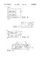
- FIG. 1is a sectional view of a substrate structure
- FIG. 2 and FIG. 3are sectional views of the substrate structure of FIG. 1 after additional steps in a process in accordance with the present invention
- FIGS. 4, 5, and 6,are top plan views of the substrate structure after additional steps in the process
- FIG. 7is a sectional view as seen from the line 7--7 in FIG. 6;
- FIG. 8is a top plan view of a substantially completed structure
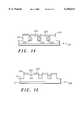
- FIGS. 9-13are a sequence of sectional views illustrating various steps in another embodiment beginning with the structure of FIG. 3;
- FIGS. 14 and 15are a sequence of sectional views illustrating various steps in another embodiment of the present invention.
- FIG. 1illustrates a substrate structure 10 including a semiconductor substrate 11 with a drift layer 12 formed thereon and a contact layer 14 formed on the upper surface of layer 12.
- substrate structure 10is formed of doped semiconductor material so as to be electrically conductive.
- substrate 11is a relatively heavily doped compound semiconductor material, such as n+ doped gallium arsenide (GaAs).
- GaAsgallium arsenide
- Layer 12is a lighter doped compound semiconductor material and preferably an epitaxially grown layer of n doped GaAs or an alloy thereof.
- Layer 14is a heavily doped compound semiconductor material and preferably an epitaxially grown layer of n+ doped GaAs or an alloy thereof.
- substrate structure 10is patterned to form a plurality of parallel, spaced apart elongated mesas 20 on or in the upper surface.
- Each mesa 20has an upper surface 21 and each adjacent pair of mesas 20 define therebetween a trench 22 with sidewalls 23 and a bottom 24.
- the patterning of substrate structure 10is performed using any standard mask and etch technique, with the etching being accomplished by using directional non-damaging reactive ion etching such as chlorine based anisotropic ECR dry etching.
- Any photoresist used in the patterning stepis stripped and the structure is D.I. water rinsed after completion of the patterning step, and a vacuum baking step is performed to eliminate any residual condensation inside trenches 22.
- a conductive material 25is then conformally deposited over mesas 20 and trenches 22, including sidewalls 23 and bottoms 24.
- conductive material 25is any material suitable for forming Schottky contacts with drift layer 12, such as TiWN or the like.
- FIG. 4a view in top plan of the structure of FIG. 3 is illustrated, including a gate feed region 27 positioned adjacent the ends of mesas 20.
- gate feed region 27can be an etched area at the same level as bottoms 24 of trenches 22, a mesa-like structure with the upper surface at the same level as surfaces 21 of mesas 20, or any selected convenient level in between.
- conductive material 25can be deposited on gate feed region 27 to provide a gate contact, if convenient, or metallization can be performed on gate feed region 27 at some later time, as will be apparent presently.
- Photoresistis deposited over the structure generally in the region denoted by broken line 30 which includes mesas 20, trenches 22, and gate feed region 27.
- a suitable plasma etchsuch as oxygen plasma, is used to etch away the photoresist overlying mesas 20 and trenches 22, leaving a layer 31 of photoresist covering gate feed region 27, as illustrated in FIG. 5.
- a directional reactive ion etch with good selectivity over photoresistis then used to etch away conductive material 25 on bottoms 24 of trenches 22 and on upper surfaces 21 of mesas 20 while leaving conductive fingers 35 on sidewalls 23 of trenches 22 and in gate feed region 27, as illustrated in FIGS. 6 and 7.
- a preferrable directional reactive ion etch for this procedureis a fluorine based anisotropic dry etch.
- Conductive materialis deposited at areas 36 to connect conductive fingers 35 to conductive material in gate feed region 27, if present, or to deposit conductive material in gate feed region 27 if not present from a previous step.
- a gate contact 37is deposited in gate feed region 27 to provide an external connection to all of conductive fingers 35.
- source contacts 38are deposited on the upper surfaces 21 of mesas 20 and a drain contact is deposited on the reverse surface of substrate 11.
- the gate contact 37 and the source and drain contactsare all ohmic contacts with source contacts 38 being shallow penetration ohmic contacts to avoid the enhanced alloying/diffusion due to more surface area created by trenches 22 around mesas 20.
- a substrate structure 110is illustrated which is similar to substrate structure 10 of FIG. 1 (including substrate 111 and layers 112 and 114). Also, substrate structure 110 is patterned, as explained in conjunction with FIG. 2, to form a plurality of elongated parallel spaced apart mesas 120, each having an upper surface 121 and each adjacent pair of mesas 120 defining therebetween a trench 122 with sidewalls 123 and a bottom 124. Further, a uniform layer of conductive material 125 is deposited over mesas 120 and trenches 122, including sidewalls 123 and bottoms 124.
- a layer 131 of photoresistis formed over the structure and a reactive ion etch is used to uniformly etch away a portion of the thickness of layer 131, reducing the thickness so as to expose conductive material 125 on upper surfaces 121 of mesas 120 and a portion of sidewalls 123, generally below layer 114, as illustrated in FIG. 11.
- the etching of layer 131 of photoresistis preferably performed using oxygen based isotropic dry etching.
- a directional reactive ion etch with good selectivity over photoresistis then used to etch away the exposed conductive material 125 leaving bottoms 124 and portions of sidewalls 123 in each trench 122 covered with conductive material 125 which serves as a gate contact.
- layer 131 of photoresistare then removed by any convenient process, as illustrated in FIG. 13.
- Ohmic contacts 138are deposited on upper surfaces 121 of each mesa 120 to form source contacts and a drain contact is formed by depositing a layer 140 of conductive material on the reverse side of substrate 111. All of the gate contacts in individual trenches 122 can then be connected to a common externally accessible gate contact (not shown) by some method, such as that described above.
- a substrate structure 210is illustrated which is similar to substrate structure 10 of FIG. 1 (including substrate 211 and layers 212 and 214). Also, substrate structure 210 is patterned, as explained in conjunction with FIG. 2, to form a plurality of elongated parallel spaced apart mesas 220, each having an upper surface 221 and each adjacent pair of mesas 220 defining therebetween a trench 222 with sidewalls 223 and a bottom 224. Further, a uniform layer of conductive material 225 is deposited over mesas 220 and trenches 222, including sidewalls 223 and bottoms 224. In this embodiment, trenches 222 are formed thin enough so that conductive material 225 substantially fills trenches 222 and, thus, masking of layer 225 is not required (see FIGS. 10 and 11 for an example of masking).
- a directional reactive ion etchis then used to uniformly etch away portions of conductive material 225 leaving each trench 222 substantially filled with conductive material 225 which serves as a gate contact. Again, conductive material 225 is etched to a. point below contact layer 214 so as not to short the sources to the gates.
- a new and improved method of fabricating vertical field effect transistorsis disclosed which results in VFETs with lower capacitance and lower ON-resistance. Further, the new and improved method is less expensive, less time consuming, and simpler than prior methods. Also, the new method provides new and improved VFETs which can be conveniently fabricated in compound semiconductor materials, such as GaAs or the like and which result in high frequency, high power VFETs.
Landscapes
- Junction Field-Effect Transistors (AREA)
Abstract
Description
Claims (8)
Priority Applications (1)
| Application Number | Priority Date | Filing Date | Title |
|---|---|---|---|
| US09/119,550US6156611A (en) | 1998-07-20 | 1998-07-20 | Method of fabricating vertical FET with sidewall gate electrode |
Applications Claiming Priority (1)
| Application Number | Priority Date | Filing Date | Title |
|---|---|---|---|
| US09/119,550US6156611A (en) | 1998-07-20 | 1998-07-20 | Method of fabricating vertical FET with sidewall gate electrode |
Publications (1)
| Publication Number | Publication Date |
|---|---|
| US6156611Atrue US6156611A (en) | 2000-12-05 |
Family
ID=22385010
Family Applications (1)
| Application Number | Title | Priority Date | Filing Date |
|---|---|---|---|
| US09/119,550Expired - Fee RelatedUS6156611A (en) | 1998-07-20 | 1998-07-20 | Method of fabricating vertical FET with sidewall gate electrode |
Country Status (1)
| Country | Link |
|---|---|
| US (1) | US6156611A (en) |
Cited By (101)
| Publication number | Priority date | Publication date | Assignee | Title |
|---|---|---|---|---|
| US6309918B1 (en)* | 1998-09-21 | 2001-10-30 | Motorola, Inc. | Manufacturable GaAs VFET process |
| US20030006455A1 (en)* | 2001-06-14 | 2003-01-09 | Ixys Corporation | Semiconductor devices having group III-V compound layers |
| US6710418B1 (en) | 2002-10-11 | 2004-03-23 | Fairchild Semiconductor Corporation | Schottky rectifier with insulation-filled trenches and method of forming the same |
| US6710403B2 (en) | 2002-07-30 | 2004-03-23 | Fairchild Semiconductor Corporation | Dual trench power MOSFET |
| US6713813B2 (en) | 2001-01-30 | 2004-03-30 | Fairchild Semiconductor Corporation | Field effect transistor having a lateral depletion structure |
| US20040132252A1 (en)* | 2001-01-30 | 2004-07-08 | Merchant Bruce D. | Method of forming a field effect transistor having a lateral depletion structure |
| US6803626B2 (en) | 2002-07-18 | 2004-10-12 | Fairchild Semiconductor Corporation | Vertical charge control semiconductor device |
| US6893947B2 (en) | 2002-06-25 | 2005-05-17 | Freescale Semiconductor, Inc. | Advanced RF enhancement-mode FETs with improved gate properties |
| US6916745B2 (en) | 2003-05-20 | 2005-07-12 | Fairchild Semiconductor Corporation | Structure and method for forming a trench MOSFET having self-aligned features |
| US6991977B2 (en) | 2001-10-17 | 2006-01-31 | Fairchild Semiconductor Corporation | Method for forming a semiconductor structure with improved smaller forward voltage loss and higher blocking capability |
| US7033891B2 (en) | 2002-10-03 | 2006-04-25 | Fairchild Semiconductor Corporation | Trench gate laterally diffused MOSFET devices and methods for making such devices |
| US20060113561A1 (en)* | 2004-12-01 | 2006-06-01 | Igor Sankin | Lateral trench field-effect transistors in wide bandgap semiconductor materials, methods of making, and integrated circuits incorporating the transistors |
| US20060113593A1 (en)* | 2004-12-01 | 2006-06-01 | Igor Sankin | Normally-off integrated JFET power switches in wide bandgap semiconductors and methods of making |
| US7061066B2 (en) | 2001-10-17 | 2006-06-13 | Fairchild Semiconductor Corporation | Schottky diode using charge balance structure |
| US7078296B2 (en) | 2002-01-16 | 2006-07-18 | Fairchild Semiconductor Corporation | Self-aligned trench MOSFETs and methods for making the same |
| US20060226477A1 (en)* | 2005-03-29 | 2006-10-12 | Brar Berinder P S | Substrate driven field-effect transistor |
| US20060226478A1 (en)* | 2005-03-29 | 2006-10-12 | Brar Berinder P S | Semiconductor device having a lateral channel and contacts on opposing surfaces thereof |
| US7132712B2 (en) | 2002-11-05 | 2006-11-07 | Fairchild Semiconductor Corporation | Trench structure having one or more diodes embedded therein adjacent a PN junction |
| US20060255360A1 (en)* | 2005-05-13 | 2006-11-16 | Brar Berinder P S | Semiconductor device having multiple lateral channels and method of forming the same |
| US20070045765A1 (en)* | 2005-08-25 | 2007-03-01 | Brar Berinder P | Semiconductor device having substrate-driven field-effect transistor and schottky diode and method of forming the same |
| US20070069286A1 (en)* | 2005-09-27 | 2007-03-29 | Brar Berinder P S | Semiconductor device having an interconnect with sloped walls and method of forming the same |
| US20070187717A1 (en)* | 2005-05-13 | 2007-08-16 | Coldwatt, Inc. | Semiconductor device having reduced on-resistance and method of forming the same |
| US7265416B2 (en) | 2002-02-23 | 2007-09-04 | Fairchild Korea Semiconductor Ltd. | High breakdown voltage low on-resistance lateral DMOS transistor |
| US7265415B2 (en) | 2004-10-08 | 2007-09-04 | Fairchild Semiconductor Corporation | MOS-gated transistor with reduced miller capacitance |
| US7280026B2 (en) | 2002-04-18 | 2007-10-09 | Coldwatt, Inc. | Extended E matrix integrated magnetics (MIM) core |
| US7298118B2 (en) | 2005-02-23 | 2007-11-20 | Coldwatt, Inc. | Power converter employing a tapped inductor and integrated magnetics and method of operating the same |
| US7301203B2 (en) | 2003-11-28 | 2007-11-27 | Fairchild Korea Semiconductor Ltd. | Superjunction semiconductor device |
| US20070296028A1 (en)* | 2006-06-21 | 2007-12-27 | Brar Berinder P S | Vertical Field-Effect Transistor and Method of Forming the Same |
| US7319256B1 (en) | 2006-06-19 | 2008-01-15 | Fairchild Semiconductor Corporation | Shielded gate trench FET with the shield and gate electrodes being connected together |
| US7321283B2 (en) | 2004-08-19 | 2008-01-22 | Coldwatt, Inc. | Vertical winding structures for planar magnetic switched-mode power converters |
| US20080048173A1 (en)* | 2005-08-25 | 2008-02-28 | Sadaka Mariam G | Semiconductor Device Including a Lateral Field-Effect Transistor and Schottky Diode |
| US7345342B2 (en) | 2001-01-30 | 2008-03-18 | Fairchild Semiconductor Corporation | Power semiconductor devices and methods of manufacture |
| US7352036B2 (en) | 2004-08-03 | 2008-04-01 | Fairchild Semiconductor Corporation | Semiconductor power device having a top-side drain using a sinker trench |
| US7368777B2 (en) | 2003-12-30 | 2008-05-06 | Fairchild Semiconductor Corporation | Accumulation device with charge balance structure and method of forming the same |
| US7385375B2 (en) | 2005-02-23 | 2008-06-10 | Coldwatt, Inc. | Control circuit for a depletion mode switch and method of operating the same |
| US7385248B2 (en) | 2005-08-09 | 2008-06-10 | Fairchild Semiconductor Corporation | Shielded gate field effect transistor with improved inter-poly dielectric |
| US7417875B2 (en) | 2005-02-08 | 2008-08-26 | Coldwatt, Inc. | Power converter employing integrated magnetics with a current multiplier rectifier and method of operating the same |
| US7427910B2 (en) | 2004-08-19 | 2008-09-23 | Coldwatt, Inc. | Winding structure for efficient switch-mode power converters |
| US20080258184A1 (en)* | 2004-07-08 | 2008-10-23 | Igor Sankin | Normally-off integrated JFET power switches in wide bandgap semiconductors and methods of making |
| US7446374B2 (en) | 2006-03-24 | 2008-11-04 | Fairchild Semiconductor Corporation | High density trench FET with integrated Schottky diode and method of manufacture |
| US7504306B2 (en) | 2005-04-06 | 2009-03-17 | Fairchild Semiconductor Corporation | Method of forming trench gate field effect transistor with recessed mesas |
| US7576388B1 (en) | 2002-10-03 | 2009-08-18 | Fairchild Semiconductor Corporation | Trench-gate LDMOS structures |
| US7625793B2 (en) | 1999-12-20 | 2009-12-01 | Fairchild Semiconductor Corporation | Power MOS device with improved gate charge performance |
| US7638841B2 (en) | 2003-05-20 | 2009-12-29 | Fairchild Semiconductor Corporation | Power semiconductor devices and methods of manufacture |
| US7663183B2 (en) | 2006-06-21 | 2010-02-16 | Flextronics International Usa, Inc. | Vertical field-effect transistor and method of forming the same |
| US7667986B2 (en) | 2006-12-01 | 2010-02-23 | Flextronics International Usa, Inc. | Power system with power converters having an adaptive controller |
| US7675759B2 (en) | 2006-12-01 | 2010-03-09 | Flextronics International Usa, Inc. | Power system with power converters having an adaptive controller |
| US7675758B2 (en) | 2006-12-01 | 2010-03-09 | Flextronics International Usa, Inc. | Power converter with an adaptive controller and method of operating the same |
| US7745289B2 (en) | 2000-08-16 | 2010-06-29 | Fairchild Semiconductor Corporation | Method of forming a FET having ultra-low on-resistance and low gate charge |
| US7772668B2 (en) | 2007-12-26 | 2010-08-10 | Fairchild Semiconductor Corporation | Shielded gate trench FET with multiple channels |
| US7876191B2 (en) | 2005-02-23 | 2011-01-25 | Flextronics International Usa, Inc. | Power converter employing a tapped inductor and integrated magnetics and method of operating the same |
| US7889517B2 (en) | 2006-12-01 | 2011-02-15 | Flextronics International Usa, Inc. | Power system with power converters having an adaptive controller |
| US7906941B2 (en) | 2007-06-19 | 2011-03-15 | Flextronics International Usa, Inc. | System and method for estimating input power for a power processing circuit |
| US8125205B2 (en) | 2006-08-31 | 2012-02-28 | Flextronics International Usa, Inc. | Power converter employing regulators with a coupled inductor |
| US8300454B2 (en) | 2010-09-17 | 2012-10-30 | Micron Technology, Inc. | Spin torque transfer memory cell structures and methods |
| US8310868B2 (en) | 2010-09-17 | 2012-11-13 | Micron Technology, Inc. | Spin torque transfer memory cell structures and methods |
| US8319290B2 (en) | 2010-06-18 | 2012-11-27 | Fairchild Semiconductor Corporation | Trench MOS barrier schottky rectifier with a planar surface using CMP techniques |
| US8358534B2 (en) | 2010-09-17 | 2013-01-22 | Micron Technology, Inc. | Spin torque transfer memory cell structures and methods |
| US8415737B2 (en) | 2006-06-21 | 2013-04-09 | Flextronics International Usa, Inc. | Semiconductor device with a pillar region and method of forming the same |
| US8502520B2 (en) | 2007-03-14 | 2013-08-06 | Flextronics International Usa, Inc | Isolated power converter |
| US8514593B2 (en) | 2009-06-17 | 2013-08-20 | Power Systems Technologies, Ltd. | Power converter employing a variable switching frequency and a magnetic device with a non-uniform gap |
| US8520414B2 (en) | 2009-01-19 | 2013-08-27 | Power Systems Technologies, Ltd. | Controller for a power converter |
| US8520420B2 (en) | 2009-12-18 | 2013-08-27 | Power Systems Technologies, Ltd. | Controller for modifying dead time between switches in a power converter |
| US8638578B2 (en) | 2009-08-14 | 2014-01-28 | Power System Technologies, Ltd. | Power converter including a charge pump employable in a power adapter |
| US8643222B2 (en) | 2009-06-17 | 2014-02-04 | Power Systems Technologies Ltd | Power adapter employing a power reducer |
| US8652901B1 (en) | 2013-03-03 | 2014-02-18 | International Business Machines Corporation | Single-mask spacer technique for semiconductor device features |
| US8673700B2 (en) | 2011-04-27 | 2014-03-18 | Fairchild Semiconductor Corporation | Superjunction structures for power devices and methods of manufacture |
| US8767418B2 (en) | 2010-03-17 | 2014-07-01 | Power Systems Technologies Ltd. | Control system for a power converter and method of operating the same |
| US8772868B2 (en) | 2011-04-27 | 2014-07-08 | Fairchild Semiconductor Corporation | Superjunction structures for power devices and methods of manufacture |
| US8787043B2 (en) | 2010-01-22 | 2014-07-22 | Power Systems Technologies, Ltd. | Controller for a power converter and method of operating the same |
| US8786010B2 (en) | 2011-04-27 | 2014-07-22 | Fairchild Semiconductor Corporation | Superjunction structures for power devices and methods of manufacture |
| US8792257B2 (en) | 2011-03-25 | 2014-07-29 | Power Systems Technologies, Ltd. | Power converter with reduced power dissipation |
| US8792256B2 (en) | 2012-01-27 | 2014-07-29 | Power Systems Technologies Ltd. | Controller for a switch and method of operating the same |
| US20140256100A1 (en)* | 2013-03-06 | 2014-09-11 | International Business Machines Corporation | Electrical coupling of memory cell access devices to a word line |
| US8835256B1 (en) | 2013-03-15 | 2014-09-16 | International Business Machines Corporation | Memory array with self-aligned epitaxially grown memory elements and annular FET |
| US8836028B2 (en) | 2011-04-27 | 2014-09-16 | Fairchild Semiconductor Corporation | Superjunction structures for power devices and methods of manufacture |
| US8928077B2 (en) | 2007-09-21 | 2015-01-06 | Fairchild Semiconductor Corporation | Superjunction structures for power devices |
| US8963212B2 (en) | 2008-12-08 | 2015-02-24 | Fairchild Semiconductor Corporation | Trench-based power semiconductor devices with increased breakdown voltage characteristics |
| US8976549B2 (en) | 2009-12-03 | 2015-03-10 | Power Systems Technologies, Ltd. | Startup circuit including first and second Schmitt triggers and power converter employing the same |
| US9019061B2 (en) | 2009-03-31 | 2015-04-28 | Power Systems Technologies, Ltd. | Magnetic device formed with U-shaped core pieces and power converter employing the same |
| US9077248B2 (en) | 2009-06-17 | 2015-07-07 | Power Systems Technologies Ltd | Start-up circuit for a power adapter |
| US9088216B2 (en) | 2009-01-19 | 2015-07-21 | Power Systems Technologies, Ltd. | Controller for a synchronous rectifier switch |
| US9099232B2 (en) | 2012-07-16 | 2015-08-04 | Power Systems Technologies Ltd. | Magnetic device and power converter employing the same |
| US9106130B2 (en) | 2012-07-16 | 2015-08-11 | Power Systems Technologies, Inc. | Magnetic device and power converter employing the same |
| US9190898B2 (en) | 2012-07-06 | 2015-11-17 | Power Systems Technologies, Ltd | Controller for a power converter and method of operating the same |
| US9197132B2 (en) | 2006-12-01 | 2015-11-24 | Flextronics International Usa, Inc. | Power converter with an adaptive controller and method of operating the same |
| US9214264B2 (en) | 2012-07-16 | 2015-12-15 | Power Systems Technologies, Ltd. | Magnetic device and power converter employing the same |
| US9240712B2 (en) | 2012-12-13 | 2016-01-19 | Power Systems Technologies Ltd. | Controller including a common current-sense device for power switches of a power converter |
| US9246391B2 (en) | 2010-01-22 | 2016-01-26 | Power Systems Technologies Ltd. | Controller for providing a corrected signal to a sensed peak current through a circuit element of a power converter |
| US9300206B2 (en) | 2013-11-15 | 2016-03-29 | Power Systems Technologies Ltd. | Method for estimating power of a power converter |
| US9379629B2 (en) | 2012-07-16 | 2016-06-28 | Power Systems Technologies, Ltd. | Magnetic device and power converter employing the same |
| US9431481B2 (en) | 2008-09-19 | 2016-08-30 | Fairchild Semiconductor Corporation | Superjunction structures for power devices and methods of manufacture |
| US9666639B2 (en) | 2010-09-17 | 2017-05-30 | Micron Technology, Inc. | Spin torque transfer memory cell structures and methods |
| US9721845B1 (en) | 2016-04-26 | 2017-08-01 | International Business Machines Corporation | Vertical field effect transistors with bottom contact metal directly beneath fins |
| US10026653B2 (en) | 2015-12-16 | 2018-07-17 | International Business Machines Corporation | Variable gate lengths for vertical transistors |
| US10062752B1 (en) | 2017-10-25 | 2018-08-28 | International Business Machines Corporation | Fabrication of nanowire vertical gate devices |
| US10396208B2 (en) | 2017-01-13 | 2019-08-27 | International Business Machines Corporation | Vertical transistors with improved top source/drain junctions |
| US10461172B2 (en) | 2017-12-21 | 2019-10-29 | International Business Machines Corporation | Vertical transistors having improved gate length control using uniformly deposited spacers |
| US10665694B2 (en) | 2017-08-21 | 2020-05-26 | International Business Machines Corporation | Vertical transistors having improved gate length control |
| US10672887B2 (en) | 2017-12-12 | 2020-06-02 | International Business Machines Corporation | Vertical FET with shaped spacer to reduce parasitic capacitance |
| KR20200130097A (en)* | 2019-05-10 | 2020-11-18 | 삼성전자주식회사 | Methods for vfet cell placement and cell architecture |
Citations (7)
| Publication number | Priority date | Publication date | Assignee | Title |
|---|---|---|---|---|
| US4262296A (en)* | 1979-07-27 | 1981-04-14 | General Electric Company | Vertical field effect transistor with improved gate and channel structure |
| US4295924A (en)* | 1979-12-17 | 1981-10-20 | International Business Machines Corporation | Method for providing self-aligned conductor in a V-groove device |
| US4568958A (en)* | 1984-01-03 | 1986-02-04 | General Electric Company | Inversion-mode insulated-gate gallium arsenide field-effect transistors |
| US4847214A (en)* | 1988-04-18 | 1989-07-11 | Motorola Inc. | Method for filling trenches from a seed layer |
| US5447874A (en)* | 1994-07-29 | 1995-09-05 | Grivna; Gordon | Method for making a semiconductor device comprising a dual metal gate using a chemical mechanical polish |
| US5705830A (en)* | 1996-09-05 | 1998-01-06 | Northrop Grumman Corporation | Static induction transistors |
| US5949124A (en)* | 1995-10-31 | 1999-09-07 | Motorola, Inc. | Edge termination structure |
- 1998
- 1998-07-20USUS09/119,550patent/US6156611A/ennot_activeExpired - Fee Related
Patent Citations (7)
| Publication number | Priority date | Publication date | Assignee | Title |
|---|---|---|---|---|
| US4262296A (en)* | 1979-07-27 | 1981-04-14 | General Electric Company | Vertical field effect transistor with improved gate and channel structure |
| US4295924A (en)* | 1979-12-17 | 1981-10-20 | International Business Machines Corporation | Method for providing self-aligned conductor in a V-groove device |
| US4568958A (en)* | 1984-01-03 | 1986-02-04 | General Electric Company | Inversion-mode insulated-gate gallium arsenide field-effect transistors |
| US4847214A (en)* | 1988-04-18 | 1989-07-11 | Motorola Inc. | Method for filling trenches from a seed layer |
| US5447874A (en)* | 1994-07-29 | 1995-09-05 | Grivna; Gordon | Method for making a semiconductor device comprising a dual metal gate using a chemical mechanical polish |
| US5949124A (en)* | 1995-10-31 | 1999-09-07 | Motorola, Inc. | Edge termination structure |
| US5705830A (en)* | 1996-09-05 | 1998-01-06 | Northrop Grumman Corporation | Static induction transistors |
Cited By (193)
| Publication number | Priority date | Publication date | Assignee | Title |
|---|---|---|---|---|
| US6309918B1 (en)* | 1998-09-21 | 2001-10-30 | Motorola, Inc. | Manufacturable GaAs VFET process |
| US7625793B2 (en) | 1999-12-20 | 2009-12-01 | Fairchild Semiconductor Corporation | Power MOS device with improved gate charge performance |
| US8710584B2 (en) | 2000-08-16 | 2014-04-29 | Fairchild Semiconductor Corporation | FET device having ultra-low on-resistance and low gate charge |
| US7745289B2 (en) | 2000-08-16 | 2010-06-29 | Fairchild Semiconductor Corporation | Method of forming a FET having ultra-low on-resistance and low gate charge |
| US8101484B2 (en) | 2000-08-16 | 2012-01-24 | Fairchild Semiconductor Corporation | Method of forming a FET having ultra-low on-resistance and low gate charge |
| US9368587B2 (en) | 2001-01-30 | 2016-06-14 | Fairchild Semiconductor Corporation | Accumulation-mode field effect transistor with improved current capability |
| US6713813B2 (en) | 2001-01-30 | 2004-03-30 | Fairchild Semiconductor Corporation | Field effect transistor having a lateral depletion structure |
| US7345342B2 (en) | 2001-01-30 | 2008-03-18 | Fairchild Semiconductor Corporation | Power semiconductor devices and methods of manufacture |
| US6818513B2 (en) | 2001-01-30 | 2004-11-16 | Fairchild Semiconductor Corporation | Method of forming a field effect transistor having a lateral depletion structure |
| US20040132252A1 (en)* | 2001-01-30 | 2004-07-08 | Merchant Bruce D. | Method of forming a field effect transistor having a lateral depletion structure |
| US8829641B2 (en) | 2001-01-30 | 2014-09-09 | Fairchild Semiconductor Corporation | Method of forming a dual-trench field effect transistor |
| US20030006455A1 (en)* | 2001-06-14 | 2003-01-09 | Ixys Corporation | Semiconductor devices having group III-V compound layers |
| US6734476B2 (en) | 2001-06-14 | 2004-05-11 | Ixys Corporation | Semiconductor devices having group III-V compound layers |
| US7429523B2 (en) | 2001-10-17 | 2008-09-30 | Fairchild Semiconductor Corporation | Method of forming schottky diode with charge balance structure |
| US7061066B2 (en) | 2001-10-17 | 2006-06-13 | Fairchild Semiconductor Corporation | Schottky diode using charge balance structure |
| US6991977B2 (en) | 2001-10-17 | 2006-01-31 | Fairchild Semiconductor Corporation | Method for forming a semiconductor structure with improved smaller forward voltage loss and higher blocking capability |
| US7078296B2 (en) | 2002-01-16 | 2006-07-18 | Fairchild Semiconductor Corporation | Self-aligned trench MOSFETs and methods for making the same |
| US7265416B2 (en) | 2002-02-23 | 2007-09-04 | Fairchild Korea Semiconductor Ltd. | High breakdown voltage low on-resistance lateral DMOS transistor |
| US7605040B2 (en) | 2002-02-23 | 2009-10-20 | Fairchild Korea Semiconductor Ltd. | Method of forming high breakdown voltage low on-resistance lateral DMOS transistor |
| US8134443B2 (en) | 2002-04-18 | 2012-03-13 | Flextronics International Usa, Inc. | Extended E matrix integrated magnetics (MIM) core |
| US7633369B2 (en) | 2002-04-18 | 2009-12-15 | Flextronics International Usa, Inc. | Extended E matrix integrated magnetics (MIM) core |
| US7280026B2 (en) | 2002-04-18 | 2007-10-09 | Coldwatt, Inc. | Extended E matrix integrated magnetics (MIM) core |
| US6893947B2 (en) | 2002-06-25 | 2005-05-17 | Freescale Semiconductor, Inc. | Advanced RF enhancement-mode FETs with improved gate properties |
| US7291894B2 (en) | 2002-07-18 | 2007-11-06 | Fairchild Semiconductor Corporation | Vertical charge control semiconductor device with low output capacitance |
| US6803626B2 (en) | 2002-07-18 | 2004-10-12 | Fairchild Semiconductor Corporation | Vertical charge control semiconductor device |
| US7977744B2 (en) | 2002-07-18 | 2011-07-12 | Fairchild Semiconductor Corporation | Field effect transistor with trench filled with insulating material and strips of semi-insulating material along trench sidewalls |
| US6710403B2 (en) | 2002-07-30 | 2004-03-23 | Fairchild Semiconductor Corporation | Dual trench power MOSFET |
| US7576388B1 (en) | 2002-10-03 | 2009-08-18 | Fairchild Semiconductor Corporation | Trench-gate LDMOS structures |
| US8198677B2 (en) | 2002-10-03 | 2012-06-12 | Fairchild Semiconductor Corporation | Trench-gate LDMOS structures |
| US7033891B2 (en) | 2002-10-03 | 2006-04-25 | Fairchild Semiconductor Corporation | Trench gate laterally diffused MOSFET devices and methods for making such devices |
| US6710418B1 (en) | 2002-10-11 | 2004-03-23 | Fairchild Semiconductor Corporation | Schottky rectifier with insulation-filled trenches and method of forming the same |
| US7132712B2 (en) | 2002-11-05 | 2006-11-07 | Fairchild Semiconductor Corporation | Trench structure having one or more diodes embedded therein adjacent a PN junction |
| US7582519B2 (en) | 2002-11-05 | 2009-09-01 | Fairchild Semiconductor Corporation | Method of forming a trench structure having one or more diodes embedded therein adjacent a PN junction |
| US8013391B2 (en) | 2003-05-20 | 2011-09-06 | Fairchild Semiconductor Corporation | Power semiconductor devices with trenched shielded split gate transistor and methods of manufacture |
| US8129245B2 (en) | 2003-05-20 | 2012-03-06 | Fairchild Semiconductor Corporation | Methods of manufacturing power semiconductor devices with shield and gate contacts |
| US8786045B2 (en) | 2003-05-20 | 2014-07-22 | Fairchild Semiconductor Corporation | Power semiconductor devices having termination structures |
| US6916745B2 (en) | 2003-05-20 | 2005-07-12 | Fairchild Semiconductor Corporation | Structure and method for forming a trench MOSFET having self-aligned features |
| US7982265B2 (en) | 2003-05-20 | 2011-07-19 | Fairchild Semiconductor Corporation | Trenched shield gate power semiconductor devices and methods of manufacture |
| US7855415B2 (en) | 2003-05-20 | 2010-12-21 | Fairchild Semiconductor Corporation | Power semiconductor devices having termination structures and methods of manufacture |
| US7799636B2 (en) | 2003-05-20 | 2010-09-21 | Fairchild Semiconductor Corporation | Power device with trenches having wider upper portion than lower portion |
| US8013387B2 (en) | 2003-05-20 | 2011-09-06 | Fairchild Semiconductor Corporation | Power semiconductor devices with shield and gate contacts and methods of manufacture |
| US8034682B2 (en) | 2003-05-20 | 2011-10-11 | Fairchild Semiconductor Corporation | Power device with trenches having wider upper portion than lower portion |
| US8889511B2 (en) | 2003-05-20 | 2014-11-18 | Fairchild Semiconductor Corporation | Methods of manufacturing power semiconductor devices with trenched shielded split gate transistor |
| US8936985B2 (en) | 2003-05-20 | 2015-01-20 | Fairchild Semiconductor Corporation | Methods related to power semiconductor devices with thick bottom oxide layers |
| US7595524B2 (en) | 2003-05-20 | 2009-09-29 | Fairchild Semiconductor Corporation | Power device with trenches having wider upper portion than lower portion |
| US8143124B2 (en) | 2003-05-20 | 2012-03-27 | Fairchild Semiconductor Corporation | Methods of making power semiconductor devices with thick bottom oxide layer |
| US7344943B2 (en) | 2003-05-20 | 2008-03-18 | Fairchild Semiconductor Corporation | Method for forming a trench MOSFET having self-aligned features |
| US8350317B2 (en) | 2003-05-20 | 2013-01-08 | Fairchild Semiconductor Corporation | Power semiconductor devices and methods of manufacture |
| US8716783B2 (en) | 2003-05-20 | 2014-05-06 | Fairchild Semiconductor Corporation | Power device with self-aligned source regions |
| US7652326B2 (en) | 2003-05-20 | 2010-01-26 | Fairchild Semiconductor Corporation | Power semiconductor devices and methods of manufacture |
| US7638841B2 (en) | 2003-05-20 | 2009-12-29 | Fairchild Semiconductor Corporation | Power semiconductor devices and methods of manufacture |
| US8143123B2 (en) | 2003-05-20 | 2012-03-27 | Fairchild Semiconductor Corporation | Methods of forming inter-poly dielectric (IPD) layers in power semiconductor devices |
| US7655981B2 (en) | 2003-11-28 | 2010-02-02 | Fairchild Korea Semiconductor Ltd. | Superjunction semiconductor device |
| US7301203B2 (en) | 2003-11-28 | 2007-11-27 | Fairchild Korea Semiconductor Ltd. | Superjunction semiconductor device |
| US7368777B2 (en) | 2003-12-30 | 2008-05-06 | Fairchild Semiconductor Corporation | Accumulation device with charge balance structure and method of forming the same |
| US8518777B2 (en) | 2003-12-30 | 2013-08-27 | Fairchild Semiconductor Corporation | Method for forming accumulation-mode field effect transistor with improved current capability |
| US7936008B2 (en) | 2003-12-30 | 2011-05-03 | Fairchild Semiconductor Corporation | Structure and method for forming accumulation-mode field effect transistor with improved current capability |
| US7820511B2 (en) | 2004-07-08 | 2010-10-26 | Semisouth Laboratories, Inc. | Normally-off integrated JFET power switches in wide bandgap semiconductors and methods of making |
| US20080258184A1 (en)* | 2004-07-08 | 2008-10-23 | Igor Sankin | Normally-off integrated JFET power switches in wide bandgap semiconductors and methods of making |
| US20100295102A1 (en)* | 2004-07-08 | 2010-11-25 | Semisouth Laboratories, Inc. | Normally-off integrated jfet power switches in wide bandgap semiconductors and methods of making |
| US20070243668A1 (en)* | 2004-07-08 | 2007-10-18 | Igor Sankin | Normally-off integrated JFET power switches in wide bandgap semiconductors and methods of making |
| US8017981B2 (en) | 2004-07-08 | 2011-09-13 | Semisouth Laboratories, Inc. | Normally-off integrated JFET power switches in wide bandgap semiconductors and methods of making |
| US7556994B2 (en) | 2004-07-08 | 2009-07-07 | Semisouth Laboratories, Inc. | Normally-off integrated JFET power switches in wide bandgap semiconductors and methods of making |
| US7352036B2 (en) | 2004-08-03 | 2008-04-01 | Fairchild Semiconductor Corporation | Semiconductor power device having a top-side drain using a sinker trench |
| US8148233B2 (en) | 2004-08-03 | 2012-04-03 | Fairchild Semiconductor Corporation | Semiconductor power device having a top-side drain using a sinker trench |
| US7732876B2 (en) | 2004-08-03 | 2010-06-08 | Fairchild Semiconductor Corporation | Power transistor with trench sinker for contacting the backside |
| US8026558B2 (en) | 2004-08-03 | 2011-09-27 | Fairchild Semiconductor Corporation | Semiconductor power device having a top-side drain using a sinker trench |
| US7554430B2 (en) | 2004-08-19 | 2009-06-30 | Flextronics International Usa, Inc. | Vertical winding structures for planar magnetic switched-mode power converters |
| US7427910B2 (en) | 2004-08-19 | 2008-09-23 | Coldwatt, Inc. | Winding structure for efficient switch-mode power converters |
| US7321283B2 (en) | 2004-08-19 | 2008-01-22 | Coldwatt, Inc. | Vertical winding structures for planar magnetic switched-mode power converters |
| US7265415B2 (en) | 2004-10-08 | 2007-09-04 | Fairchild Semiconductor Corporation | MOS-gated transistor with reduced miller capacitance |
| US7534683B2 (en) | 2004-10-08 | 2009-05-19 | Fairchild Semiconductor Corporation | Method of making a MOS-gated transistor with reduced miller capacitance |
| US7242040B2 (en) | 2004-12-01 | 2007-07-10 | Semisouth Laboratories, Inc. | Lateral trench field-effect transistors in wide bandgap semiconductor materials, methods of making, and integrated circuits incorporating the transistors |
| US20060113561A1 (en)* | 2004-12-01 | 2006-06-01 | Igor Sankin | Lateral trench field-effect transistors in wide bandgap semiconductor materials, methods of making, and integrated circuits incorporating the transistors |
| US20070012946A1 (en)* | 2004-12-01 | 2007-01-18 | Igor Sankin | Lateral trench field-effect transistors in wide bandgap semiconductor materials, methods of making, and integrated circuits incorporating the transistors |
| US7202528B2 (en) | 2004-12-01 | 2007-04-10 | Semisouth Laboratories, Inc. | Normally-off integrated JFET power switches in wide bandgap semiconductors and methods of making |
| US7119380B2 (en) | 2004-12-01 | 2006-10-10 | Semisouth Laboratories, Inc. | Lateral trench field-effect transistors in wide bandgap semiconductor materials, methods of making, and integrated circuits incorporating the transistors |
| US20060113593A1 (en)* | 2004-12-01 | 2006-06-01 | Igor Sankin | Normally-off integrated JFET power switches in wide bandgap semiconductors and methods of making |
| EP2375451A2 (en) | 2004-12-01 | 2011-10-12 | Semisouth Laboratories, Inc. | Lateral trench field-effect transistors in wide bandgap semiconductor materials, methods of making, and integrated circuits incorporating the transistors |
| US8502282B2 (en) | 2004-12-01 | 2013-08-06 | Power Integrations, Inc. | Normally-off integrated JFET power switches in wide bandgap semiconductors and methods of making |
| US7417875B2 (en) | 2005-02-08 | 2008-08-26 | Coldwatt, Inc. | Power converter employing integrated magnetics with a current multiplier rectifier and method of operating the same |
| US7675764B2 (en) | 2005-02-08 | 2010-03-09 | Flextronics International Usa, Inc. | Power converter employing integrated magnetics with a current multiplier rectifier and method of operating the same |
| US7385375B2 (en) | 2005-02-23 | 2008-06-10 | Coldwatt, Inc. | Control circuit for a depletion mode switch and method of operating the same |
| US7876191B2 (en) | 2005-02-23 | 2011-01-25 | Flextronics International Usa, Inc. | Power converter employing a tapped inductor and integrated magnetics and method of operating the same |
| US7298118B2 (en) | 2005-02-23 | 2007-11-20 | Coldwatt, Inc. | Power converter employing a tapped inductor and integrated magnetics and method of operating the same |
| US20070145417A1 (en)* | 2005-03-29 | 2007-06-28 | Brar Berinder P S | High voltage semiconductor device having a lateral channel and enhanced gate-to-drain separation |
| US20060226477A1 (en)* | 2005-03-29 | 2006-10-12 | Brar Berinder P S | Substrate driven field-effect transistor |
| US20060226478A1 (en)* | 2005-03-29 | 2006-10-12 | Brar Berinder P S | Semiconductor device having a lateral channel and contacts on opposing surfaces thereof |
| US7439556B2 (en) | 2005-03-29 | 2008-10-21 | Coldwatt, Inc. | Substrate driven field-effect transistor |
| US7439557B2 (en) | 2005-03-29 | 2008-10-21 | Coldwatt, Inc. | Semiconductor device having a lateral channel and contacts on opposing surfaces thereof |
| US8680611B2 (en) | 2005-04-06 | 2014-03-25 | Fairchild Semiconductor Corporation | Field effect transistor and schottky diode structures |
| US7504306B2 (en) | 2005-04-06 | 2009-03-17 | Fairchild Semiconductor Corporation | Method of forming trench gate field effect transistor with recessed mesas |
| US8084327B2 (en) | 2005-04-06 | 2011-12-27 | Fairchild Semiconductor Corporation | Method for forming trench gate field effect transistor with recessed mesas using spacers |
| US20070187717A1 (en)* | 2005-05-13 | 2007-08-16 | Coldwatt, Inc. | Semiconductor device having reduced on-resistance and method of forming the same |
| US7339208B2 (en) | 2005-05-13 | 2008-03-04 | Coldwatt, Inc. | Semiconductor device having multiple lateral channels and method of forming the same |
| US7838905B2 (en) | 2005-05-13 | 2010-11-23 | Flextronics International Usa, Inc. | Semiconductor device having multiple lateral channels and method of forming the same |
| US7675090B2 (en) | 2005-05-13 | 2010-03-09 | Flextronics International Usa, Inc. | Semiconductor device having a contact on a buffer layer thereof and method of forming the same |
| US20060255360A1 (en)* | 2005-05-13 | 2006-11-16 | Brar Berinder P S | Semiconductor device having multiple lateral channels and method of forming the same |
| US7598144B2 (en) | 2005-08-09 | 2009-10-06 | Fairchild Semiconductor Corporation | Method for forming inter-poly dielectric in shielded gate field effect transistor |
| US7385248B2 (en) | 2005-08-09 | 2008-06-10 | Fairchild Semiconductor Corporation | Shielded gate field effect transistor with improved inter-poly dielectric |
| US20070045765A1 (en)* | 2005-08-25 | 2007-03-01 | Brar Berinder P | Semiconductor device having substrate-driven field-effect transistor and schottky diode and method of forming the same |
| US20080048174A1 (en)* | 2005-08-25 | 2008-02-28 | Sadaka Mariam G | Semiconductor Device Including a Lateral Field-Effect Transistor and Schottky Diode |
| US7642568B2 (en) | 2005-08-25 | 2010-01-05 | Flextronics International Usa, Inc. | Semiconductor device having substrate-driven field-effect transistor and Schottky diode and method of forming the same |
| US20080048173A1 (en)* | 2005-08-25 | 2008-02-28 | Sadaka Mariam G | Semiconductor Device Including a Lateral Field-Effect Transistor and Schottky Diode |
| US7655963B2 (en) | 2005-08-25 | 2010-02-02 | Flextronics International Usa, Inc. | Semiconductor device including a lateral field-effect transistor and Schottky diode |
| US7564074B2 (en) | 2005-08-25 | 2009-07-21 | Flextronics International Usa, Inc. | Semiconductor device including a lateral field-effect transistor and Schottky diode |
| US7504673B2 (en) | 2005-08-25 | 2009-03-17 | Flextronics International Usa, Inc. | Semiconductor device including a lateral field-effect transistor and Schottky diode |
| US20080054304A1 (en)* | 2005-08-25 | 2008-03-06 | Sadaka Mariam G | Semiconductor Device Including a Lateral Field-Effect Transistor and Schottky Diode |
| US7285807B2 (en) | 2005-08-25 | 2007-10-23 | Coldwatt, Inc. | Semiconductor device having substrate-driven field-effect transistor and Schottky diode and method of forming the same |
| US20080048219A1 (en)* | 2005-08-25 | 2008-02-28 | Brar Berinder P S | Semiconductor Device Having Substrate-Driven Field-Effect Transistor and Schottky Diode and Method of Forming the Same |
| US7462891B2 (en) | 2005-09-27 | 2008-12-09 | Coldwatt, Inc. | Semiconductor device having an interconnect with sloped walls and method of forming the same |
| US20070069286A1 (en)* | 2005-09-27 | 2007-03-29 | Brar Berinder P S | Semiconductor device having an interconnect with sloped walls and method of forming the same |
| US7446374B2 (en) | 2006-03-24 | 2008-11-04 | Fairchild Semiconductor Corporation | High density trench FET with integrated Schottky diode and method of manufacture |
| US7713822B2 (en) | 2006-03-24 | 2010-05-11 | Fairchild Semiconductor Corporation | Method of forming high density trench FET with integrated Schottky diode |
| US7859047B2 (en) | 2006-06-19 | 2010-12-28 | Fairchild Semiconductor Corporation | Shielded gate trench FET with the shield and gate electrodes connected together in non-active region |
| US7319256B1 (en) | 2006-06-19 | 2008-01-15 | Fairchild Semiconductor Corporation | Shielded gate trench FET with the shield and gate electrodes being connected together |
| US7473603B2 (en) | 2006-06-19 | 2009-01-06 | Fairchild Semiconductor Corporation | Method for forming a shielded gate trench FET with the shield and gate electrodes being connected together |
| US7541640B2 (en) | 2006-06-21 | 2009-06-02 | Flextronics International Usa, Inc. | Vertical field-effect transistor and method of forming the same |
| US20070296028A1 (en)* | 2006-06-21 | 2007-12-27 | Brar Berinder P S | Vertical Field-Effect Transistor and Method of Forming the Same |
| US7663183B2 (en) | 2006-06-21 | 2010-02-16 | Flextronics International Usa, Inc. | Vertical field-effect transistor and method of forming the same |
| US8415737B2 (en) | 2006-06-21 | 2013-04-09 | Flextronics International Usa, Inc. | Semiconductor device with a pillar region and method of forming the same |
| US8125205B2 (en) | 2006-08-31 | 2012-02-28 | Flextronics International Usa, Inc. | Power converter employing regulators with a coupled inductor |
| US7889517B2 (en) | 2006-12-01 | 2011-02-15 | Flextronics International Usa, Inc. | Power system with power converters having an adaptive controller |
| US9197132B2 (en) | 2006-12-01 | 2015-11-24 | Flextronics International Usa, Inc. | Power converter with an adaptive controller and method of operating the same |
| US8477514B2 (en) | 2006-12-01 | 2013-07-02 | Flextronics International Usa, Inc. | Power system with power converters having an adaptive controller |
| US7675758B2 (en) | 2006-12-01 | 2010-03-09 | Flextronics International Usa, Inc. | Power converter with an adaptive controller and method of operating the same |
| US7675759B2 (en) | 2006-12-01 | 2010-03-09 | Flextronics International Usa, Inc. | Power system with power converters having an adaptive controller |
| US7667986B2 (en) | 2006-12-01 | 2010-02-23 | Flextronics International Usa, Inc. | Power system with power converters having an adaptive controller |
| US8502520B2 (en) | 2007-03-14 | 2013-08-06 | Flextronics International Usa, Inc | Isolated power converter |
| US7906941B2 (en) | 2007-06-19 | 2011-03-15 | Flextronics International Usa, Inc. | System and method for estimating input power for a power processing circuit |
| US9595596B2 (en) | 2007-09-21 | 2017-03-14 | Fairchild Semiconductor Corporation | Superjunction structures for power devices |
| US8928077B2 (en) | 2007-09-21 | 2015-01-06 | Fairchild Semiconductor Corporation | Superjunction structures for power devices |
| US9224853B2 (en) | 2007-12-26 | 2015-12-29 | Fairchild Semiconductor Corporation | Shielded gate trench FET with multiple channels |
| US7772668B2 (en) | 2007-12-26 | 2010-08-10 | Fairchild Semiconductor Corporation | Shielded gate trench FET with multiple channels |
| US9431481B2 (en) | 2008-09-19 | 2016-08-30 | Fairchild Semiconductor Corporation | Superjunction structures for power devices and methods of manufacture |
| US8963212B2 (en) | 2008-12-08 | 2015-02-24 | Fairchild Semiconductor Corporation | Trench-based power semiconductor devices with increased breakdown voltage characteristics |
| US9391193B2 (en) | 2008-12-08 | 2016-07-12 | Fairchild Semiconductor Corporation | Trench-based power semiconductor devices with increased breakdown voltage characteristics |
| US9088216B2 (en) | 2009-01-19 | 2015-07-21 | Power Systems Technologies, Ltd. | Controller for a synchronous rectifier switch |
| US8520414B2 (en) | 2009-01-19 | 2013-08-27 | Power Systems Technologies, Ltd. | Controller for a power converter |
| US9019061B2 (en) | 2009-03-31 | 2015-04-28 | Power Systems Technologies, Ltd. | Magnetic device formed with U-shaped core pieces and power converter employing the same |
| US8514593B2 (en) | 2009-06-17 | 2013-08-20 | Power Systems Technologies, Ltd. | Power converter employing a variable switching frequency and a magnetic device with a non-uniform gap |
| US8643222B2 (en) | 2009-06-17 | 2014-02-04 | Power Systems Technologies Ltd | Power adapter employing a power reducer |
| US9077248B2 (en) | 2009-06-17 | 2015-07-07 | Power Systems Technologies Ltd | Start-up circuit for a power adapter |
| US8638578B2 (en) | 2009-08-14 | 2014-01-28 | Power System Technologies, Ltd. | Power converter including a charge pump employable in a power adapter |
| US8976549B2 (en) | 2009-12-03 | 2015-03-10 | Power Systems Technologies, Ltd. | Startup circuit including first and second Schmitt triggers and power converter employing the same |
| US8520420B2 (en) | 2009-12-18 | 2013-08-27 | Power Systems Technologies, Ltd. | Controller for modifying dead time between switches in a power converter |
| US8787043B2 (en) | 2010-01-22 | 2014-07-22 | Power Systems Technologies, Ltd. | Controller for a power converter and method of operating the same |
| US9246391B2 (en) | 2010-01-22 | 2016-01-26 | Power Systems Technologies Ltd. | Controller for providing a corrected signal to a sensed peak current through a circuit element of a power converter |
| US8767418B2 (en) | 2010-03-17 | 2014-07-01 | Power Systems Technologies Ltd. | Control system for a power converter and method of operating the same |
| US8319290B2 (en) | 2010-06-18 | 2012-11-27 | Fairchild Semiconductor Corporation | Trench MOS barrier schottky rectifier with a planar surface using CMP techniques |
| US8432000B2 (en) | 2010-06-18 | 2013-04-30 | Fairchild Semiconductor Corporation | Trench MOS barrier schottky rectifier with a planar surface using CMP techniques |
| US8472244B2 (en) | 2010-09-17 | 2013-06-25 | Micron Technology, Inc. | Spin torque transfer memory cell structures and methods |
| US8767455B2 (en) | 2010-09-17 | 2014-07-01 | Micron Technology, Inc. | Spin torque transfer memory cell structures and methods |
| US8310868B2 (en) | 2010-09-17 | 2012-11-13 | Micron Technology, Inc. | Spin torque transfer memory cell structures and methods |
| US9666639B2 (en) | 2010-09-17 | 2017-05-30 | Micron Technology, Inc. | Spin torque transfer memory cell structures and methods |
| US8804414B2 (en) | 2010-09-17 | 2014-08-12 | Micron Technology, Inc. | Spin torque transfer memory cell structures and methods |
| US8358534B2 (en) | 2010-09-17 | 2013-01-22 | Micron Technology, Inc. | Spin torque transfer memory cell structures and methods |
| US8300454B2 (en) | 2010-09-17 | 2012-10-30 | Micron Technology, Inc. | Spin torque transfer memory cell structures and methods |
| US8792257B2 (en) | 2011-03-25 | 2014-07-29 | Power Systems Technologies, Ltd. | Power converter with reduced power dissipation |
| US8673700B2 (en) | 2011-04-27 | 2014-03-18 | Fairchild Semiconductor Corporation | Superjunction structures for power devices and methods of manufacture |
| US8836028B2 (en) | 2011-04-27 | 2014-09-16 | Fairchild Semiconductor Corporation | Superjunction structures for power devices and methods of manufacture |
| US8786010B2 (en) | 2011-04-27 | 2014-07-22 | Fairchild Semiconductor Corporation | Superjunction structures for power devices and methods of manufacture |
| US8772868B2 (en) | 2011-04-27 | 2014-07-08 | Fairchild Semiconductor Corporation | Superjunction structures for power devices and methods of manufacture |
| US8792256B2 (en) | 2012-01-27 | 2014-07-29 | Power Systems Technologies Ltd. | Controller for a switch and method of operating the same |
| US9190898B2 (en) | 2012-07-06 | 2015-11-17 | Power Systems Technologies, Ltd | Controller for a power converter and method of operating the same |
| US9214264B2 (en) | 2012-07-16 | 2015-12-15 | Power Systems Technologies, Ltd. | Magnetic device and power converter employing the same |
| US9099232B2 (en) | 2012-07-16 | 2015-08-04 | Power Systems Technologies Ltd. | Magnetic device and power converter employing the same |
| US9106130B2 (en) | 2012-07-16 | 2015-08-11 | Power Systems Technologies, Inc. | Magnetic device and power converter employing the same |
| US9379629B2 (en) | 2012-07-16 | 2016-06-28 | Power Systems Technologies, Ltd. | Magnetic device and power converter employing the same |
| US9240712B2 (en) | 2012-12-13 | 2016-01-19 | Power Systems Technologies Ltd. | Controller including a common current-sense device for power switches of a power converter |
| US8652901B1 (en) | 2013-03-03 | 2014-02-18 | International Business Machines Corporation | Single-mask spacer technique for semiconductor device features |
| US8658498B1 (en) | 2013-03-03 | 2014-02-25 | International Business Machines Corporation | Single mask spacer technique for semiconductor device features |
| US9299804B2 (en)* | 2013-03-06 | 2016-03-29 | International Business Machines Corporation | Electrical coupling of memory cell access devices to a word line |
| US9343545B2 (en) | 2013-03-06 | 2016-05-17 | International Business Machines Corporation | Electrical coupling of memory cell access devices to a word line |
| US20140256100A1 (en)* | 2013-03-06 | 2014-09-11 | International Business Machines Corporation | Electrical coupling of memory cell access devices to a word line |
| US8901529B2 (en) | 2013-03-15 | 2014-12-02 | International Business Machines Corporation | Memory array with self-aligned epitaxially grown memory elements and annular FET |
| US8835256B1 (en) | 2013-03-15 | 2014-09-16 | International Business Machines Corporation | Memory array with self-aligned epitaxially grown memory elements and annular FET |
| US9300206B2 (en) | 2013-11-15 | 2016-03-29 | Power Systems Technologies Ltd. | Method for estimating power of a power converter |
| US10395992B2 (en) | 2015-12-16 | 2019-08-27 | International Business Machines Corporation | Variable gate lengths for vertical transistors |
| US10026653B2 (en) | 2015-12-16 | 2018-07-17 | International Business Machines Corporation | Variable gate lengths for vertical transistors |
| US10714396B2 (en) | 2015-12-16 | 2020-07-14 | International Business Machines Corporation | Variable gate lengths for vertical transistors |
| US9721845B1 (en) | 2016-04-26 | 2017-08-01 | International Business Machines Corporation | Vertical field effect transistors with bottom contact metal directly beneath fins |
| US10396208B2 (en) | 2017-01-13 | 2019-08-27 | International Business Machines Corporation | Vertical transistors with improved top source/drain junctions |
| US10680081B2 (en) | 2017-01-13 | 2020-06-09 | International Business Machines Corporation | Vertical transistors with improved top source/drain junctions |
| US10665694B2 (en) | 2017-08-21 | 2020-05-26 | International Business Machines Corporation | Vertical transistors having improved gate length control |
| US10672888B2 (en) | 2017-08-21 | 2020-06-02 | International Business Machines Corporation | Vertical transistors having improved gate length control |
| US10347717B2 (en) | 2017-10-25 | 2019-07-09 | International Business Machines Corporation | Fabrication of nanowire vertical gate devices |
| US10062752B1 (en) | 2017-10-25 | 2018-08-28 | International Business Machines Corporation | Fabrication of nanowire vertical gate devices |
| US10672887B2 (en) | 2017-12-12 | 2020-06-02 | International Business Machines Corporation | Vertical FET with shaped spacer to reduce parasitic capacitance |
| US10903338B2 (en) | 2017-12-12 | 2021-01-26 | International Business Machines Corporation | Vertical FET with shaped spacer to reduce parasitic capacitance |
| US10461172B2 (en) | 2017-12-21 | 2019-10-29 | International Business Machines Corporation | Vertical transistors having improved gate length control using uniformly deposited spacers |
| KR20200130097A (en)* | 2019-05-10 | 2020-11-18 | 삼성전자주식회사 | Methods for vfet cell placement and cell architecture |
| US11468221B2 (en)* | 2019-05-10 | 2022-10-11 | Samsung Electronics Co.. Ltd. | Methods for VFET cell placement and cell architecture |
Similar Documents
| Publication | Publication Date | Title |
|---|---|---|
| US6156611A (en) | Method of fabricating vertical FET with sidewall gate electrode | |
| US4711858A (en) | Method of fabricating a self-aligned metal-semiconductor FET having an insulator spacer | |
| US5473176A (en) | Vertical insulated gate transistor and method of manufacture | |
| US5742082A (en) | Stable FET with shielding region in the substrate | |
| CN110233104A (en) | High electron mobility transistor with double thickness barrier layers | |
| US5550065A (en) | Method of fabricating self-aligned FET structure having a high temperature stable T-shaped Schottky gate contact | |
| JP2009517883A (en) | Metal semiconductor field effect transistor having channels with different thicknesses and method for manufacturing the same | |
| US5336626A (en) | Method of manufacturing a MESFET with an epitaxial void | |
| US5877047A (en) | Lateral gate, vertical drift region transistor | |
| US6090716A (en) | Method of fabricating a field effect transistor | |
| US5702975A (en) | Method for isolating semiconductor device | |
| US5814548A (en) | Process for making n-channel or p-channel permeable base transistor with a plurality layers | |
| US5837570A (en) | Heterostructure semiconductor device and method of fabricating same | |
| US5719088A (en) | Method of fabricating semiconductor devices with a passivated surface | |
| US4774555A (en) | Power hemt structure | |
| US5274257A (en) | Floating channel field effect transistor and a fabricating method thereof | |
| KR100629020B1 (en) | SiC side field effect transistor, a method of manufacturing the same, and a method of using the transistor | |
| JPH08330325A (en) | Field effect transistor and manufacturing method | |
| KR100198425B1 (en) | Method of manufacturing heterojunction bipolar transistor | |
| CN119008405B (en) | Preparation method of self-aligned grid GaN HEMT device | |
| US20080064155A1 (en) | Method for Producing a Multi-Stage Recess in a Layer Structure and a Field Effect Transistor with a Multi-Recessed Gate | |
| JP2689960B2 (en) | Semiconductor device | |
| TWI890422B (en) | Semiconductor device and method of fabricating the same | |
| JP2000124228A (en) | Method for manufacturing semiconductor device | |
| KR20040065560A (en) | A field effect transistor semiconductor device |
Legal Events
| Date | Code | Title | Description |
|---|---|---|---|
| AS | Assignment | Owner name:MOTOROLA, INC., ILLINOIS Free format text:ASSIGNMENT OF ASSIGNORS INTEREST;ASSIGNORS:LAN, ELLEN;HUANG, JENN-HWA;EISENBEISER, KURT;AND OTHERS;REEL/FRAME:009336/0713 Effective date:19980715 | |
| AS | Assignment | Owner name:FREESCALE SEMICONDUCTOR, INC., TEXAS Free format text:ASSIGNMENT OF ASSIGNORS INTEREST;ASSIGNOR:MOTOROLA, INC.;REEL/FRAME:015698/0657 Effective date:20040404 Owner name:FREESCALE SEMICONDUCTOR, INC.,TEXAS Free format text:ASSIGNMENT OF ASSIGNORS INTEREST;ASSIGNOR:MOTOROLA, INC.;REEL/FRAME:015698/0657 Effective date:20040404 | |
| FPAY | Fee payment | Year of fee payment:4 | |
| AS | Assignment | Owner name:CITIBANK, N.A. AS COLLATERAL AGENT, NEW YORK Free format text:SECURITY AGREEMENT;ASSIGNORS:FREESCALE SEMICONDUCTOR, INC.;FREESCALE ACQUISITION CORPORATION;FREESCALE ACQUISITION HOLDINGS CORP.;AND OTHERS;REEL/FRAME:018855/0129 Effective date:20061201 Owner name:CITIBANK, N.A. AS COLLATERAL AGENT,NEW YORK Free format text:SECURITY AGREEMENT;ASSIGNORS:FREESCALE SEMICONDUCTOR, INC.;FREESCALE ACQUISITION CORPORATION;FREESCALE ACQUISITION HOLDINGS CORP.;AND OTHERS;REEL/FRAME:018855/0129 Effective date:20061201 | |
| REMI | Maintenance fee reminder mailed | ||
| LAPS | Lapse for failure to pay maintenance fees | ||
| STCH | Information on status: patent discontinuation | Free format text:PATENT EXPIRED DUE TO NONPAYMENT OF MAINTENANCE FEES UNDER 37 CFR 1.362 | |
| FP | Lapsed due to failure to pay maintenance fee | Effective date:20081205 | |
| AS | Assignment | Owner name:FREESCALE SEMICONDUCTOR, INC., TEXAS Free format text:PATENT RELEASE;ASSIGNOR:CITIBANK, N.A., AS COLLATERAL AGENT;REEL/FRAME:037354/0225 Effective date:20151207 |