US6156171A - Sputtering magnetron - Google Patents
Sputtering magnetronDownload PDFInfo
- Publication number
- US6156171A US6156171AUS08/045,989US4598993AUS6156171AUS 6156171 AUS6156171 AUS 6156171AUS 4598993 AUS4598993 AUS 4598993AUS 6156171 AUS6156171 AUS 6156171A
- Authority
- US
- United States
- Prior art keywords
- sputtering
- substrates
- chamber
- target
- chambers
- Prior art date
- Legal status (The legal status is an assumption and is not a legal conclusion. Google has not performed a legal analysis and makes no representation as to the accuracy of the status listed.)
- Expired - Lifetime
Links
Images


Classifications
- H—ELECTRICITY
- H01—ELECTRIC ELEMENTS
- H01L—SEMICONDUCTOR DEVICES NOT COVERED BY CLASS H10
- H01L21/00—Processes or apparatus adapted for the manufacture or treatment of semiconductor or solid state devices or of parts thereof
- H01L21/67—Apparatus specially adapted for handling semiconductor or electric solid state devices during manufacture or treatment thereof; Apparatus specially adapted for handling wafers during manufacture or treatment of semiconductor or electric solid state devices or components ; Apparatus not specifically provided for elsewhere
- H01L21/677—Apparatus specially adapted for handling semiconductor or electric solid state devices during manufacture or treatment thereof; Apparatus specially adapted for handling wafers during manufacture or treatment of semiconductor or electric solid state devices or components ; Apparatus not specifically provided for elsewhere for conveying, e.g. between different workstations
- H01L21/67739—Apparatus specially adapted for handling semiconductor or electric solid state devices during manufacture or treatment thereof; Apparatus specially adapted for handling wafers during manufacture or treatment of semiconductor or electric solid state devices or components ; Apparatus not specifically provided for elsewhere for conveying, e.g. between different workstations into and out of processing chamber
- H01L21/6776—Continuous loading and unloading into and out of a processing chamber, e.g. transporting belts within processing chambers
- C—CHEMISTRY; METALLURGY
- C23—COATING METALLIC MATERIAL; COATING MATERIAL WITH METALLIC MATERIAL; CHEMICAL SURFACE TREATMENT; DIFFUSION TREATMENT OF METALLIC MATERIAL; COATING BY VACUUM EVAPORATION, BY SPUTTERING, BY ION IMPLANTATION OR BY CHEMICAL VAPOUR DEPOSITION, IN GENERAL; INHIBITING CORROSION OF METALLIC MATERIAL OR INCRUSTATION IN GENERAL
- C23C—COATING METALLIC MATERIAL; COATING MATERIAL WITH METALLIC MATERIAL; SURFACE TREATMENT OF METALLIC MATERIAL BY DIFFUSION INTO THE SURFACE, BY CHEMICAL CONVERSION OR SUBSTITUTION; COATING BY VACUUM EVAPORATION, BY SPUTTERING, BY ION IMPLANTATION OR BY CHEMICAL VAPOUR DEPOSITION, IN GENERAL
- C23C14/00—Coating by vacuum evaporation, by sputtering or by ion implantation of the coating forming material
- C23C14/02—Pretreatment of the material to be coated
- C23C14/028—Physical treatment to alter the texture of the substrate surface, e.g. grinding, polishing
- C—CHEMISTRY; METALLURGY
- C23—COATING METALLIC MATERIAL; COATING MATERIAL WITH METALLIC MATERIAL; CHEMICAL SURFACE TREATMENT; DIFFUSION TREATMENT OF METALLIC MATERIAL; COATING BY VACUUM EVAPORATION, BY SPUTTERING, BY ION IMPLANTATION OR BY CHEMICAL VAPOUR DEPOSITION, IN GENERAL; INHIBITING CORROSION OF METALLIC MATERIAL OR INCRUSTATION IN GENERAL
- C23C—COATING METALLIC MATERIAL; COATING MATERIAL WITH METALLIC MATERIAL; SURFACE TREATMENT OF METALLIC MATERIAL BY DIFFUSION INTO THE SURFACE, BY CHEMICAL CONVERSION OR SUBSTITUTION; COATING BY VACUUM EVAPORATION, BY SPUTTERING, BY ION IMPLANTATION OR BY CHEMICAL VAPOUR DEPOSITION, IN GENERAL
- C23C14/00—Coating by vacuum evaporation, by sputtering or by ion implantation of the coating forming material
- C23C14/22—Coating by vacuum evaporation, by sputtering or by ion implantation of the coating forming material characterised by the process of coating
- C23C14/34—Sputtering
- C23C14/35—Sputtering by application of a magnetic field, e.g. magnetron sputtering
- C23C14/352—Sputtering by application of a magnetic field, e.g. magnetron sputtering using more than one target
- C—CHEMISTRY; METALLURGY
- C23—COATING METALLIC MATERIAL; COATING MATERIAL WITH METALLIC MATERIAL; CHEMICAL SURFACE TREATMENT; DIFFUSION TREATMENT OF METALLIC MATERIAL; COATING BY VACUUM EVAPORATION, BY SPUTTERING, BY ION IMPLANTATION OR BY CHEMICAL VAPOUR DEPOSITION, IN GENERAL; INHIBITING CORROSION OF METALLIC MATERIAL OR INCRUSTATION IN GENERAL
- C23C—COATING METALLIC MATERIAL; COATING MATERIAL WITH METALLIC MATERIAL; SURFACE TREATMENT OF METALLIC MATERIAL BY DIFFUSION INTO THE SURFACE, BY CHEMICAL CONVERSION OR SUBSTITUTION; COATING BY VACUUM EVAPORATION, BY SPUTTERING, BY ION IMPLANTATION OR BY CHEMICAL VAPOUR DEPOSITION, IN GENERAL
- C23C14/00—Coating by vacuum evaporation, by sputtering or by ion implantation of the coating forming material
- C23C14/22—Coating by vacuum evaporation, by sputtering or by ion implantation of the coating forming material characterised by the process of coating
- C23C14/50—Substrate holders
- C—CHEMISTRY; METALLURGY
- C23—COATING METALLIC MATERIAL; COATING MATERIAL WITH METALLIC MATERIAL; CHEMICAL SURFACE TREATMENT; DIFFUSION TREATMENT OF METALLIC MATERIAL; COATING BY VACUUM EVAPORATION, BY SPUTTERING, BY ION IMPLANTATION OR BY CHEMICAL VAPOUR DEPOSITION, IN GENERAL; INHIBITING CORROSION OF METALLIC MATERIAL OR INCRUSTATION IN GENERAL
- C23C—COATING METALLIC MATERIAL; COATING MATERIAL WITH METALLIC MATERIAL; SURFACE TREATMENT OF METALLIC MATERIAL BY DIFFUSION INTO THE SURFACE, BY CHEMICAL CONVERSION OR SUBSTITUTION; COATING BY VACUUM EVAPORATION, BY SPUTTERING, BY ION IMPLANTATION OR BY CHEMICAL VAPOUR DEPOSITION, IN GENERAL
- C23C14/00—Coating by vacuum evaporation, by sputtering or by ion implantation of the coating forming material
- C23C14/22—Coating by vacuum evaporation, by sputtering or by ion implantation of the coating forming material characterised by the process of coating
- C23C14/54—Controlling or regulating the coating process
- C23C14/541—Heating or cooling of the substrates
- C—CHEMISTRY; METALLURGY
- C23—COATING METALLIC MATERIAL; COATING MATERIAL WITH METALLIC MATERIAL; CHEMICAL SURFACE TREATMENT; DIFFUSION TREATMENT OF METALLIC MATERIAL; COATING BY VACUUM EVAPORATION, BY SPUTTERING, BY ION IMPLANTATION OR BY CHEMICAL VAPOUR DEPOSITION, IN GENERAL; INHIBITING CORROSION OF METALLIC MATERIAL OR INCRUSTATION IN GENERAL
- C23C—COATING METALLIC MATERIAL; COATING MATERIAL WITH METALLIC MATERIAL; SURFACE TREATMENT OF METALLIC MATERIAL BY DIFFUSION INTO THE SURFACE, BY CHEMICAL CONVERSION OR SUBSTITUTION; COATING BY VACUUM EVAPORATION, BY SPUTTERING, BY ION IMPLANTATION OR BY CHEMICAL VAPOUR DEPOSITION, IN GENERAL
- C23C14/00—Coating by vacuum evaporation, by sputtering or by ion implantation of the coating forming material
- C23C14/22—Coating by vacuum evaporation, by sputtering or by ion implantation of the coating forming material characterised by the process of coating
- C23C14/56—Apparatus specially adapted for continuous coating; Arrangements for maintaining the vacuum, e.g. vacuum locks
- C23C14/568—Transferring the substrates through a series of coating stations
- G—PHYSICS
- G05—CONTROLLING; REGULATING
- G05B—CONTROL OR REGULATING SYSTEMS IN GENERAL; FUNCTIONAL ELEMENTS OF SUCH SYSTEMS; MONITORING OR TESTING ARRANGEMENTS FOR SUCH SYSTEMS OR ELEMENTS
- G05B19/00—Programme-control systems
- G05B19/02—Programme-control systems electric
- G05B19/04—Programme control other than numerical control, i.e. in sequence controllers or logic controllers
- G05B19/05—Programmable logic controllers, e.g. simulating logic interconnections of signals according to ladder diagrams or function charts
- G05B19/052—Linking several PLC's
- G—PHYSICS
- G05—CONTROLLING; REGULATING
- G05B—CONTROL OR REGULATING SYSTEMS IN GENERAL; FUNCTIONAL ELEMENTS OF SUCH SYSTEMS; MONITORING OR TESTING ARRANGEMENTS FOR SUCH SYSTEMS OR ELEMENTS
- G05B19/00—Programme-control systems
- G05B19/02—Programme-control systems electric
- G05B19/418—Total factory control, i.e. centrally controlling a plurality of machines, e.g. direct or distributed numerical control [DNC], flexible manufacturing systems [FMS], integrated manufacturing systems [IMS] or computer integrated manufacturing [CIM]
- G05B19/4189—Total factory control, i.e. centrally controlling a plurality of machines, e.g. direct or distributed numerical control [DNC], flexible manufacturing systems [FMS], integrated manufacturing systems [IMS] or computer integrated manufacturing [CIM] characterised by the transport system
- G—PHYSICS
- G11—INFORMATION STORAGE
- G11B—INFORMATION STORAGE BASED ON RELATIVE MOVEMENT BETWEEN RECORD CARRIER AND TRANSDUCER
- G11B5/00—Recording by magnetisation or demagnetisation of a record carrier; Reproducing by magnetic means; Record carriers therefor
- G11B5/84—Processes or apparatus specially adapted for manufacturing record carriers
- G11B5/851—Coating a support with a magnetic layer by sputtering
- H—ELECTRICITY
- H01—ELECTRIC ELEMENTS
- H01J—ELECTRIC DISCHARGE TUBES OR DISCHARGE LAMPS
- H01J37/00—Discharge tubes with provision for introducing objects or material to be exposed to the discharge, e.g. for the purpose of examination or processing thereof
- H01J37/32—Gas-filled discharge tubes
- H01J37/32431—Constructional details of the reactor
- H01J37/32733—Means for moving the material to be treated
- H—ELECTRICITY
- H01—ELECTRIC ELEMENTS
- H01J—ELECTRIC DISCHARGE TUBES OR DISCHARGE LAMPS
- H01J37/00—Discharge tubes with provision for introducing objects or material to be exposed to the discharge, e.g. for the purpose of examination or processing thereof
- H01J37/32—Gas-filled discharge tubes
- H01J37/34—Gas-filled discharge tubes operating with cathodic sputtering
- H01J37/3402—Gas-filled discharge tubes operating with cathodic sputtering using supplementary magnetic fields
- H01J37/3405—Magnetron sputtering
- H—ELECTRICITY
- H01—ELECTRIC ELEMENTS
- H01L—SEMICONDUCTOR DEVICES NOT COVERED BY CLASS H10
- H01L21/00—Processes or apparatus adapted for the manufacture or treatment of semiconductor or solid state devices or of parts thereof
- H01L21/67—Apparatus specially adapted for handling semiconductor or electric solid state devices during manufacture or treatment thereof; Apparatus specially adapted for handling wafers during manufacture or treatment of semiconductor or electric solid state devices or components ; Apparatus not specifically provided for elsewhere
- H01L21/67005—Apparatus not specifically provided for elsewhere
- H01L21/67011—Apparatus for manufacture or treatment
- H01L21/6715—Apparatus for applying a liquid, a resin, an ink or the like
- H—ELECTRICITY
- H01—ELECTRIC ELEMENTS
- H01L—SEMICONDUCTOR DEVICES NOT COVERED BY CLASS H10
- H01L21/00—Processes or apparatus adapted for the manufacture or treatment of semiconductor or solid state devices or of parts thereof
- H01L21/67—Apparatus specially adapted for handling semiconductor or electric solid state devices during manufacture or treatment thereof; Apparatus specially adapted for handling wafers during manufacture or treatment of semiconductor or electric solid state devices or components ; Apparatus not specifically provided for elsewhere
- H01L21/67005—Apparatus not specifically provided for elsewhere
- H01L21/67011—Apparatus for manufacture or treatment
- H01L21/67155—Apparatus for manufacturing or treating in a plurality of work-stations
- H01L21/67161—Apparatus for manufacturing or treating in a plurality of work-stations characterized by the layout of the process chambers
- H01L21/67173—Apparatus for manufacturing or treating in a plurality of work-stations characterized by the layout of the process chambers in-line arrangement
- H—ELECTRICITY
- H01—ELECTRIC ELEMENTS
- H01L—SEMICONDUCTOR DEVICES NOT COVERED BY CLASS H10
- H01L21/00—Processes or apparatus adapted for the manufacture or treatment of semiconductor or solid state devices or of parts thereof
- H01L21/67—Apparatus specially adapted for handling semiconductor or electric solid state devices during manufacture or treatment thereof; Apparatus specially adapted for handling wafers during manufacture or treatment of semiconductor or electric solid state devices or components ; Apparatus not specifically provided for elsewhere
- H01L21/67005—Apparatus not specifically provided for elsewhere
- H01L21/67011—Apparatus for manufacture or treatment
- H01L21/67155—Apparatus for manufacturing or treating in a plurality of work-stations
- H01L21/67207—Apparatus for manufacturing or treating in a plurality of work-stations comprising a chamber adapted to a particular process
- H01L21/67213—Apparatus for manufacturing or treating in a plurality of work-stations comprising a chamber adapted to a particular process comprising at least one ion or electron beam chamber
- H—ELECTRICITY
- H01—ELECTRIC ELEMENTS
- H01L—SEMICONDUCTOR DEVICES NOT COVERED BY CLASS H10
- H01L21/00—Processes or apparatus adapted for the manufacture or treatment of semiconductor or solid state devices or of parts thereof
- H01L21/67—Apparatus specially adapted for handling semiconductor or electric solid state devices during manufacture or treatment thereof; Apparatus specially adapted for handling wafers during manufacture or treatment of semiconductor or electric solid state devices or components ; Apparatus not specifically provided for elsewhere
- H01L21/67005—Apparatus not specifically provided for elsewhere
- H01L21/67011—Apparatus for manufacture or treatment
- H01L21/67155—Apparatus for manufacturing or treating in a plurality of work-stations
- H01L21/67236—Apparatus for manufacturing or treating in a plurality of work-stations the substrates being processed being not semiconductor wafers, e.g. leadframes or chips
- H—ELECTRICITY
- H01—ELECTRIC ELEMENTS
- H01L—SEMICONDUCTOR DEVICES NOT COVERED BY CLASS H10
- H01L21/00—Processes or apparatus adapted for the manufacture or treatment of semiconductor or solid state devices or of parts thereof
- H01L21/67—Apparatus specially adapted for handling semiconductor or electric solid state devices during manufacture or treatment thereof; Apparatus specially adapted for handling wafers during manufacture or treatment of semiconductor or electric solid state devices or components ; Apparatus not specifically provided for elsewhere
- H01L21/67005—Apparatus not specifically provided for elsewhere
- H01L21/67242—Apparatus for monitoring, sorting or marking
- H01L21/67253—Process monitoring, e.g. flow or thickness monitoring
- H—ELECTRICITY
- H01—ELECTRIC ELEMENTS
- H01L—SEMICONDUCTOR DEVICES NOT COVERED BY CLASS H10
- H01L21/00—Processes or apparatus adapted for the manufacture or treatment of semiconductor or solid state devices or of parts thereof
- H01L21/67—Apparatus specially adapted for handling semiconductor or electric solid state devices during manufacture or treatment thereof; Apparatus specially adapted for handling wafers during manufacture or treatment of semiconductor or electric solid state devices or components ; Apparatus not specifically provided for elsewhere
- H01L21/67005—Apparatus not specifically provided for elsewhere
- H01L21/67242—Apparatus for monitoring, sorting or marking
- H01L21/67259—Position monitoring, e.g. misposition detection or presence detection
- H—ELECTRICITY
- H01—ELECTRIC ELEMENTS
- H01L—SEMICONDUCTOR DEVICES NOT COVERED BY CLASS H10
- H01L21/00—Processes or apparatus adapted for the manufacture or treatment of semiconductor or solid state devices or of parts thereof
- H01L21/67—Apparatus specially adapted for handling semiconductor or electric solid state devices during manufacture or treatment thereof; Apparatus specially adapted for handling wafers during manufacture or treatment of semiconductor or electric solid state devices or components ; Apparatus not specifically provided for elsewhere
- H01L21/67005—Apparatus not specifically provided for elsewhere
- H01L21/67242—Apparatus for monitoring, sorting or marking
- H01L21/67276—Production flow monitoring, e.g. for increasing throughput
- H—ELECTRICITY
- H01—ELECTRIC ELEMENTS
- H01L—SEMICONDUCTOR DEVICES NOT COVERED BY CLASS H10
- H01L21/00—Processes or apparatus adapted for the manufacture or treatment of semiconductor or solid state devices or of parts thereof
- H01L21/67—Apparatus specially adapted for handling semiconductor or electric solid state devices during manufacture or treatment thereof; Apparatus specially adapted for handling wafers during manufacture or treatment of semiconductor or electric solid state devices or components ; Apparatus not specifically provided for elsewhere
- H01L21/677—Apparatus specially adapted for handling semiconductor or electric solid state devices during manufacture or treatment thereof; Apparatus specially adapted for handling wafers during manufacture or treatment of semiconductor or electric solid state devices or components ; Apparatus not specifically provided for elsewhere for conveying, e.g. between different workstations
- H01L21/67703—Apparatus specially adapted for handling semiconductor or electric solid state devices during manufacture or treatment thereof; Apparatus specially adapted for handling wafers during manufacture or treatment of semiconductor or electric solid state devices or components ; Apparatus not specifically provided for elsewhere for conveying, e.g. between different workstations between different workstations
- H01L21/67712—Apparatus specially adapted for handling semiconductor or electric solid state devices during manufacture or treatment thereof; Apparatus specially adapted for handling wafers during manufacture or treatment of semiconductor or electric solid state devices or components ; Apparatus not specifically provided for elsewhere for conveying, e.g. between different workstations between different workstations the substrate being handled substantially vertically
- H—ELECTRICITY
- H01—ELECTRIC ELEMENTS
- H01L—SEMICONDUCTOR DEVICES NOT COVERED BY CLASS H10
- H01L21/00—Processes or apparatus adapted for the manufacture or treatment of semiconductor or solid state devices or of parts thereof
- H01L21/67—Apparatus specially adapted for handling semiconductor or electric solid state devices during manufacture or treatment thereof; Apparatus specially adapted for handling wafers during manufacture or treatment of semiconductor or electric solid state devices or components ; Apparatus not specifically provided for elsewhere
- H01L21/677—Apparatus specially adapted for handling semiconductor or electric solid state devices during manufacture or treatment thereof; Apparatus specially adapted for handling wafers during manufacture or treatment of semiconductor or electric solid state devices or components ; Apparatus not specifically provided for elsewhere for conveying, e.g. between different workstations
- H01L21/67703—Apparatus specially adapted for handling semiconductor or electric solid state devices during manufacture or treatment thereof; Apparatus specially adapted for handling wafers during manufacture or treatment of semiconductor or electric solid state devices or components ; Apparatus not specifically provided for elsewhere for conveying, e.g. between different workstations between different workstations
- H01L21/67721—Apparatus specially adapted for handling semiconductor or electric solid state devices during manufacture or treatment thereof; Apparatus specially adapted for handling wafers during manufacture or treatment of semiconductor or electric solid state devices or components ; Apparatus not specifically provided for elsewhere for conveying, e.g. between different workstations between different workstations the substrates to be conveyed not being semiconductor wafers or large planar substrates, e.g. chips, lead frames
- G—PHYSICS
- G05—CONTROLLING; REGULATING
- G05B—CONTROL OR REGULATING SYSTEMS IN GENERAL; FUNCTIONAL ELEMENTS OF SUCH SYSTEMS; MONITORING OR TESTING ARRANGEMENTS FOR SUCH SYSTEMS OR ELEMENTS
- G05B2219/00—Program-control systems
- G05B2219/30—Nc systems
- G05B2219/31—From computer integrated manufacturing till monitoring
- G05B2219/31225—System structure, plc's and pc's communicate over lan
- G—PHYSICS
- G05—CONTROLLING; REGULATING
- G05B—CONTROL OR REGULATING SYSTEMS IN GENERAL; FUNCTIONAL ELEMENTS OF SUCH SYSTEMS; MONITORING OR TESTING ARRANGEMENTS FOR SUCH SYSTEMS OR ELEMENTS
- G05B2219/00—Program-control systems
- G05B2219/30—Nc systems
- G05B2219/31—From computer integrated manufacturing till monitoring
- G05B2219/31237—Host and rs232, rs485 to network controller and rs232 to controlled devices
- G—PHYSICS
- G05—CONTROLLING; REGULATING
- G05B—CONTROL OR REGULATING SYSTEMS IN GENERAL; FUNCTIONAL ELEMENTS OF SUCH SYSTEMS; MONITORING OR TESTING ARRANGEMENTS FOR SUCH SYSTEMS OR ELEMENTS
- G05B2219/00—Program-control systems
- G05B2219/30—Nc systems
- G05B2219/32—Operator till task planning
- G05B2219/32413—Pc generates control strategy, download in plc to monitor and react to events
- G—PHYSICS
- G05—CONTROLLING; REGULATING
- G05B—CONTROL OR REGULATING SYSTEMS IN GENERAL; FUNCTIONAL ELEMENTS OF SUCH SYSTEMS; MONITORING OR TESTING ARRANGEMENTS FOR SUCH SYSTEMS OR ELEMENTS
- G05B2219/00—Program-control systems
- G05B2219/30—Nc systems
- G05B2219/34—Director, elements to supervisory
- G05B2219/34029—Pam programmable axis controller, to control large number of axis
- G—PHYSICS
- G05—CONTROLLING; REGULATING
- G05B—CONTROL OR REGULATING SYSTEMS IN GENERAL; FUNCTIONAL ELEMENTS OF SUCH SYSTEMS; MONITORING OR TESTING ARRANGEMENTS FOR SUCH SYSTEMS OR ELEMENTS
- G05B2219/00—Program-control systems
- G05B2219/30—Nc systems
- G05B2219/34—Director, elements to supervisory
- G05B2219/34279—Pc, personal computer as controller
- G—PHYSICS
- G05—CONTROLLING; REGULATING
- G05B—CONTROL OR REGULATING SYSTEMS IN GENERAL; FUNCTIONAL ELEMENTS OF SUCH SYSTEMS; MONITORING OR TESTING ARRANGEMENTS FOR SUCH SYSTEMS OR ELEMENTS
- G05B2219/00—Program-control systems
- G05B2219/30—Nc systems
- G05B2219/34—Director, elements to supervisory
- G05B2219/34287—Plc and motion controller combined
- G—PHYSICS
- G05—CONTROLLING; REGULATING
- G05B—CONTROL OR REGULATING SYSTEMS IN GENERAL; FUNCTIONAL ELEMENTS OF SUCH SYSTEMS; MONITORING OR TESTING ARRANGEMENTS FOR SUCH SYSTEMS OR ELEMENTS
- G05B2219/00—Program-control systems
- G05B2219/30—Nc systems
- G05B2219/34—Director, elements to supervisory
- G05B2219/34304—Pc as input, edit device for plc
- G—PHYSICS
- G05—CONTROLLING; REGULATING
- G05B—CONTROL OR REGULATING SYSTEMS IN GENERAL; FUNCTIONAL ELEMENTS OF SUCH SYSTEMS; MONITORING OR TESTING ARRANGEMENTS FOR SUCH SYSTEMS OR ELEMENTS
- G05B2219/00—Program-control systems
- G05B2219/30—Nc systems
- G05B2219/50—Machine tool, machine tool null till machine tool work handling
- G05B2219/50363—Load unload with two robots, one to load, other to unload
- Y—GENERAL TAGGING OF NEW TECHNOLOGICAL DEVELOPMENTS; GENERAL TAGGING OF CROSS-SECTIONAL TECHNOLOGIES SPANNING OVER SEVERAL SECTIONS OF THE IPC; TECHNICAL SUBJECTS COVERED BY FORMER USPC CROSS-REFERENCE ART COLLECTIONS [XRACs] AND DIGESTS
- Y02—TECHNOLOGIES OR APPLICATIONS FOR MITIGATION OR ADAPTATION AGAINST CLIMATE CHANGE
- Y02P—CLIMATE CHANGE MITIGATION TECHNOLOGIES IN THE PRODUCTION OR PROCESSING OF GOODS
- Y02P80/00—Climate change mitigation technologies for sector-wide applications
- Y02P80/10—Efficient use of energy, e.g. using compressed air or pressurized fluid as energy carrier
- Y—GENERAL TAGGING OF NEW TECHNOLOGICAL DEVELOPMENTS; GENERAL TAGGING OF CROSS-SECTIONAL TECHNOLOGIES SPANNING OVER SEVERAL SECTIONS OF THE IPC; TECHNICAL SUBJECTS COVERED BY FORMER USPC CROSS-REFERENCE ART COLLECTIONS [XRACs] AND DIGESTS
- Y02—TECHNOLOGIES OR APPLICATIONS FOR MITIGATION OR ADAPTATION AGAINST CLIMATE CHANGE
- Y02P—CLIMATE CHANGE MITIGATION TECHNOLOGIES IN THE PRODUCTION OR PROCESSING OF GOODS
- Y02P80/00—Climate change mitigation technologies for sector-wide applications
- Y02P80/40—Minimising material used in manufacturing processes
- Y—GENERAL TAGGING OF NEW TECHNOLOGICAL DEVELOPMENTS; GENERAL TAGGING OF CROSS-SECTIONAL TECHNOLOGIES SPANNING OVER SEVERAL SECTIONS OF THE IPC; TECHNICAL SUBJECTS COVERED BY FORMER USPC CROSS-REFERENCE ART COLLECTIONS [XRACs] AND DIGESTS
- Y02—TECHNOLOGIES OR APPLICATIONS FOR MITIGATION OR ADAPTATION AGAINST CLIMATE CHANGE
- Y02P—CLIMATE CHANGE MITIGATION TECHNOLOGIES IN THE PRODUCTION OR PROCESSING OF GOODS
- Y02P90/00—Enabling technologies with a potential contribution to greenhouse gas [GHG] emissions mitigation
- Y02P90/02—Total factory control, e.g. smart factories, flexible manufacturing systems [FMS] or integrated manufacturing systems [IMS]
Definitions
- the inventionrelates to an apparatus and method for depositing multilayer thin films in a magnetron sputtering process. More particularly, the invention relates to an apparatus and method for depositing thin magnetic films for magnetic recording media in a high volume, electronically controlled, magnetron sputtering process, and to production of an improved magnetic recording disk product thereby.
- Sputteringis a well-known technique for depositing uniform thin films on a particular substrate. Sputtering is performed in an evacuated chamber using an inert gas, typically argon, with one or more substrates remaining static during deposition, being rotated about the target (a "planetary” system) or being transported past the target (an “in-line” system).
- an inert gastypically argon
- the techniqueinvolves bombarding the surface of a target material to be deposited as the film with electrostatically accelerated argon ions.
- electric fieldsare used to accelerate ions in the plasma gas, causing them to impinge on the target surface.
- momentum transferatoms and electrons are dislodged from the target surface in an area known as the erosion region.
- Target atomsdeposit on the substrate, forming a film.
- evacuation of the sputtering chamberis a two-stage process in order to avoid contaminant-circulating turbulence in the chamber.
- a throttled roughing stageslowly pumps down the chamber to a first pressure, such as about 50 microns.
- high vacuum pumpingoccurs using turbo-, cryo- or diffusion pumps to evacuate the chamber to the highly evacuated base pressure (about 10 -7 Torr) necessary to perform sputtering.
- Sputtering gasis subsequently provided in the evacuated chamber, backfilling to a pressure of about 2-10 microns.
- the sputtering processis useful for depositing coatings from a plurality of target materials onto a variety of substrate materials, including glass, nickel-phosphorus plated aluminum disks, and ceramic materials.
- substrate materialsincluding glass, nickel-phosphorus plated aluminum disks, and ceramic materials.
- electrostatic forcesdiode sputtering
- various magnet arrangementshave been used to enhance the sputtering rate by trapping electrons close to the target surface, ionizing more argon, increasing the probability of impacting and dislodging target atoms and therefore the sputtering rate.
- an increased sputtering rateis achieved by manipulation of a magnetic field geometry in the region adjacent to the target surface.
- Sputter deposition performed in this manneris generally referred to as magnetron sputtering.
- the magnetic field geometrymay be optimized by adjusting the polarity and position of individual magnets used to generate magnetic fields with the goal of using the magnetic field flux paths to enhance the sputtering rate.
- U.S. Pat. No. 4,166,018, issued Aug. 28, 1989 to J. S. Chapin and assigned to Airco, Inc.describes a planar direct current (d.c.) magnetron sputtering apparatus which uses a magnet configuration to generate arcuate magnetic flux paths (or lines) that confine she electrons and ions in a plasma region immediately adjacent to the target erosion region.
- d.c.direct current
- a variety of magnet arrangementsare suitable for this purpose, as long as one or more closed loop paths of magnetic flux is parallel to the cathode surface, e.g., concentric ovals or circles.
- the role of the magnetic fieldis to trap moving electrons near the target.
- the fieldgenerates a force on the electrons, inducing the electrons to take a spiral path about the magnetic field lines.
- Such a spiral pathis longer than a path along the field lines, thereby increasing the chance of the electron ionizing a plasma gas atom, typically argon.
- field linesalso reduce electron repulsion away from a negatively biased target.
- a greater ion fluxis created in the plasma region adjacent to the target with a correspondingly enhanced erosion of target atoms from an area which conforms to a shape approximating the inverse shape of the field lines.
- the erosion region adjacent to the field linesconforms to a shallow track, leaving much of the target unavailable for sputtering.
- sputteringoffers the ability to tailor film properties to a considerable extent by making minor adjustments to process parameters.
- processesyielding films with specific crystalline microstructures and magnetic properties. Consequently, much research has been conducted on the effects of sputtering pressures, deposition temperature and maintenance of the evacuated environment to avoid contamination or degradation of the substrate surface before film deposition.
- Alloys of cobalt, nickel and chromium deposited on a chromium underlayerare highly desirable as films for magnetic recording media such as disks utilized in Winchester-type hard disk drives.
- in-line sputtering processescreate magnetic anisotropies which are manifested as signal waveform modulations and anomalies in the deposited films.
- Anisotropy in the direction of disk travel through such in-line processesis understood to be caused by crystalline growth perpendicular to the direction of disk travel as a result of the deposition of the obliquely incident flux of target atoms as the disk enters and exits a sputtering chamber. Since magnetic film properties depend on crystalline microstructure, such anisotropy in the chromium underlayer can disrupt the subsequent deposition of the magnetic CoNiCr layer in the preferred orientation.
- the preferred crystalline orientation for the chromium underlayeris with the closely packed, bcc ⁇ 110 ⁇ plane parallel to the film surface.
- This orientation for the chromium nucleating layerforces the ⁇ C ⁇ axis of the hcp structure of the magnetic cobalt-alloy layer, i.e., the easy axis of magnetization, to be aligned in the film plane.
- the orientation of the magnetic field generated in the sputtering processmay induce an additional anisotropy which causes similar signal waveform modulations. See, Uchinami, et al., "Magnetic Anisotropies in Sputtered Thin Film Disks", IEEE Trans. Magn., Vol. MAG-23, No.
- CoCr alloys with tantalumare particularly attractive films for magnetic recording media.
- Linear recording density of magnetic films on media used in Winchester-type hard disk drivesis known to be enhanced by decreasing the flying height of the magnetic recording head above the recording medium. With reduced flying height, there is an increased need to protect the magnetic film layer from wear. Magnetic films are also susceptible to corrosion from vapors present even at trace concentrations within the magnetic recording system.
- a variety of filmshave been employed as protective overlayers for magnetic films, including rhodium, carbon and inorganic nonmetallic carbides, nitrides and oxides, like silica or alumina.
- problemssuch as poor adhesion to the magnetic layer and inadequate wear resistance have limited the applicability of these films.
- U.S. Pat. No. 4,503,125 issued on Mar. 3, 1985 to Nelson, et al. and assigned to Xebec, Inc.describes a protective carbon overcoating for magnetic films where adhesion is enhanced by chemically bonding a sputtered layer of titanium between the magnetic layer and the carbon overcoating.
- the carbon overlayerAs the wear-resistant layer for magnetic recording media, it is desirable that the carbon overlayer have a microcrystalline structure corresponding to high hardness. In other words, it is desirable during sputtering to minimize graphitization of carbon which softens amorphous carbon films.
- One means employed to moderate graphitization of sputtered carbon filmsis by incorporating hydrogen into the film. Such incorporation may be accomplished by sputtering in an argon atmosphere mixed with hydrogen or a hydrogen-containing gas, such as methane or other hydrocarbons.
- Magnetron sputtering processeshave been developed which have been somewhat successful in achieving high throughput.
- U.S. Pat. Nos. 4,735,840 and 4,894,133issued to Hedgcoth on Apr. 5, 1988 and Apr. 16, 1990, respectively, describe a high volume planar d. c. magnetron in-line sputtering apparatus which forms multilayer magnetic recording films on disks for use in Winchester-type hard disk technology.
- the apparatusincludes several consecutive regions for sputtering individual layers within a single sputtering chamber through which preheated disk substrates mounted on a pallet or other vertical carrier proceed at velocities up to about 10 mm/sec (1.97 ft/min), though averaging only about 3 mm/sec (0.6 ft/min).
- the first sputtering regiondeposits chromium (1,000 to 5,000 ⁇ ) on a circumferentially textured disk substrate.
- the next regiondeposits a layer (200 to 1,500 ⁇ ) of a magnetic alloy such as CoNi.
- a protective layer(200 to 800 ⁇ ) of a wear- and corrosion-resistant material such as amorphous carbon is deposited.
- the apparatusis evacuated by mechanical and cryo pumps to a base pressure about 2 ⁇ 10 -7 Torr. Sputtering is performed at a relatively high argon pressure between 2 and 4 ⁇ 10 -2 Torr (20 to 40 microns) to eliminate anisotropy due to obliquely incident flux.
- substrate heatingis typically accomplished with heaters requiring an extended dwell time to warm substrates to a desired equilibrium temperature.
- substrate transport speeds through the sputtering apparatushave been limited with respect to mechanisms using traditional bottom drive, gear/belt-driven transport systems.
- Such bottom drive systemsgenerally have intermeshing gears and may be practically incapable of proceeding faster than a particular rate due to rough section-to-section transitions which may dislodge substrates from the carrier and/or create particulate matter from gear wear which contaminates the disks prior to or during the sputtering process.
- overall process throughputwould be further enhanced by the employment of heating and transport elements which require minimal time to perform these functions.
- prior art sputtering devicesutilize relatively unsophisticated means for controlling the sputtering processes described therein.
- Such control systemsmay comprise standard optical or electrical metering monitored by a system operator, with direct electrical or electro-mechanical switching of components utilized in the system by the system operator.
- Such systemshave been adequately successful for limited throughput of sputtered substrates.
- a more comprehensive systemis required for higher throughput sputtering operations.
- a control systemis required which provides to the operator an extensive amount of information concerning the ongoing process through a relatively user-friendly environment.
- the control systemmust adequately automate functions both in series and in parallel where necessary to control every aspect of the sputtering system.
- an object of the present inventionis to provide a high throughput sputtering process and apparatus.
- a further object of the present inventionis to provide a control system for the apparatus and process which continuously monitors and facilitates alteration of film deposition process parameters.
- a further object of the present inventionis to provide a high throughput sputtering apparatus with a centralized electronic control system.
- An additional object of this inventionis to provide the above objects in a means by which sputtering is achieved in a highly efficient, contaminant-free environment.
- An additional object of this inventionis to provide a highly versatile, contaminant-free means for transporting substrates through the apparatus and process.
- a further object of this inventionis to transport substrates through the sputtering apparatus by means of an overhead, gearless transport mechanism.
- a further object of this inventionis to provide a transport mechanism for carrying a plurality of substrates, each at a user-defined, variable speed.
- a further object of this inventionis to maintain a contaminant-free environment within the sputtering apparatus by means of a high speed, high capacity vacuum pump system.
- a further object of this inventionis to provide a magnetron design allowing efficient erosion of target material during the sputtering process.
- a further object of this inventionis to provide a high throughput sputtering apparatus which achieves and maintains a uniform substrate surface temperature profile before film deposition.
- a further object of this inventionis to provide a highly isotropic film by minimizing deposition by target atoms impinging on the substrate surface at high angles of incidence.
- a further object of this inventionis to provide high throughput sputtering apparatus which minimizes oxidation of the chromium underlayer before magnetic film deposition.
- An additional object of the present inventionis to provide high quality thin magnetic films on magnetic recording media with superior magnetic recording properties.
- a further object of this inventionis to provide high quality thin cobalt-chromium-tantalum (CoCrTa) films with superior magnetic recording properties.
- a further object of this inventionis to provide high quality sputtered thin magnetic films circumferentially oriented along the easy magnetic axis.
- a further object of this inventionis to provide high throughput sputtering apparatus for high quality thin carbon films with superior wear, hardness, corrosion and elastic properties.
- a further object of this inventionis to provide a method for depositing wear-resistant carbon films comprising sputtering in the presence of a hydrogen-containing gas.
- a further object of this inventionis to provide an improved method for sputtering carbon films using either an electrically biased or grounded pallet.
- An apparatus in accordance with the present inventionprovides a single or multi-layer coating to the surface of a plurality of substrates.
- Said apparatusincludes a plurality of buffer and sputtering chambers, and an input end and an output end, wherein said substrates are transported through said chambers of said apparatus at varying rates of speed such that the rate of speed of a pallet from said input end to said output end is a constant for each of said plurality of pallets.
- a high throughput sputtering apparatus having a plurality of integrally matched components in accordance with the present inventionmay comprise means for sputtering a multi-layer coating onto a plurality of substrates, said means for sputtering including a series of sputtering chambers each having relative isolation from adjacent chambers to reduce cross contamination between the coating components being sputtered onto substrates therein, said sputtering chambers being isolated from ambient atmospheric conditions; means for transporting said plurality of substrates through said means for sputtering at variable velocities; means for reducing the ambient pressure within said means for sputtering to a vacuum level within a pressure range sufficient to enable sputtering operation; means for heating said plurality of substrates to a temperature conducive to sputtering said multi-layer coatings thereon, said means for heating providing a substantially uniform temperature profile over the surface of said substrate; and control means for providing control signals to and for receiving feedback input from, said means for sputtering, means for transporting, means
- a process in accordance the present inventionincludes: providing substrates to be sputtered; creating an environment about said substrates, said environment having a pressure within a pressure range which would enable sputtering operations; providing a gas into said environment in a plasma state and within said pressure range to carry out sputtering operations; transporting substrates at varying velocities through said environment a sequence of sputtering steps within said environment and along a return path external to said environment simultaneously introducing the substrates into said environment without substantially disrupting said pressure of said environment, providing rapid and uniform heating of said substrates to optimize film integrity during sputtering steps, and sputtering said substrates to provide successive layers of thin films on the substrates; and, removing the sputtered substrates without contaminating said environment.
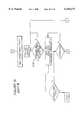
- FIG. 1is a system plan view of the sputtering apparatus of the present invention.
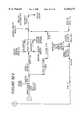
- FIG. 2is a cross sectional view along line 2--2 of the sputtering apparatus of the present invention as shown in FIG. 1.
- FIG. 3is a plan view of the sputtering apparatus of the present invention illustrating the physical relationship of the power supply and pumping subsystem components.
- FIG. 4is an overview block diagram of the sputtering process of the present invention.
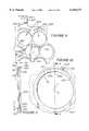
- FIG. 5is a simplified perspective view of the means for texturing disk substrates used in the process of the present invention.
- FIGS. 6A and 6Bare cross sectional views along line 6--6 of the cam wheel utilized in the means for texturing shown in FIG. 5.
- FIG. 7is a sectional magnified view of the texturing of a disk surface provided by the means for texturing disclosed in FIG. 5.
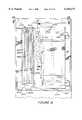
- FIG. 8is a surface view of one embodiment of a pallet for carrying disks through the sputtering apparatus of the present invention.
- FIG. 9is a partial, enlarged view of the pallet of FIG. 8.
- FIG. 10is a partial, enlarged view of one region for carrying a disk in the pallet of FIG. 9.
- FIG. 11is a cross sectional view along 11--11 of the disk carrying region shown in FIG. 10.
- FIG. 12is an overview diagram of the pumping system used with the apparatus of the present invention.
- FIG. 13is a side, partial cutaway view of a sputtering chamber utilized in the apparatus of the present invention.
- FIG. 14is an assembled cross sectional view of the substrate transport mechanism, sputtering shields, and pallet viewed along line 14--14 of FIG. 13.
- FIG. 15is a cross sectional view of the main (or “dwell”) heating lamp assembly and chamber.
- FIG. 16is a view of the main heating lamp assembly along line 16--16 in FIG. 15.
- FIG. 17is a view of the main heating lamp mounting tray and cooling lines along line 17--17 in FIG. 15.
- FIG. 18is a cross sectional view of the secondary (or “passby”) heating lamp and chamber assembly.
- FIG. 19is a view of the heating lamp assembly along line 19--19 in FIG. 18.
- FIG. 20is a view of the secondary heating lamp, mounting tray and cooling lines along line 20--20 in FIG. 18.
- FIG. 21is a perspective, partial view of a heat reflecting panel, pallet, and substrate transport system utilized in the apparatus present invention.
- FIG. 22is a perspective, exploded view of a portion of a pallet, substrate transport mechanism, sputtering shield, and cathode assembly utilized in the sputtering apparatus of the present invention.
- FIG. 23is a top view of the sputtering chamber shown in FIG. 13.
- FIG. 24is a cross-sectional, side view along line 24--24 of FIG. 23.
- FIG. 25is a partial perspective view of a first surface of the cathode portion of the magnetron of the present invention.
- FIG. 26is a perspective view of a second surface of the cathode of the magnetron of the present invention, including cooling line inputs and magnet channels of the cathode.
- FIG. 27Ais a cross-sectional, assembled view of a first embodiment of the magnet configuration in the cathode for a nonmagnetic target of the present invention along line 27--27 of FIG. 25.
- FIG. 27Bis a cross-sectional, assembled views of a second embodiment of the magnet configuration in the cathode for magnetic target of the present invention along line 27--27 of FIG. 25.
- FIG. 28is a cross sectional view of the multi-layer sputtered thin film created by the process of the present invention.
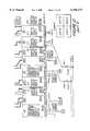
- FIG. 29is a block diagram of the electronic control system of the present invention.
- FIG. 30is a block flow chart of functional aspects of the software utilized in the process controller(s) of the present invention.
- FIG. 31is a flow chart of the automated cryogenic pump regeneration process of the present invention.
- FIGS. 32A through 32Ecomprise a single logical flow diagram outlining the software logic controlling the motor assemblies, load lock and exit lock pumping, and heater power during the automatic substrate run mode of the software utilized in the electronic control system of the present invention.
- the apparatus of the present inventionis capable of applying the multilayer coatings to any given substrate within a time frame of approximately five minutes.
- the apparatus and processmay provide production throughputs on the order of at least five times greater than those of prior art multi-layer coating processes.
- sputtering apparatus and method for high throughput sputteringinclude: flexibility with respect to the composition of the multilayer films applied and the types of substrates to which they are applied; easily interchanged coating components; a novel means for heating substrates; a novel sputtering magnetron design; a variable speed, overhead, noncontaminating substrate transportation system; and a comprehensive, centralized, programmable electronic means for controlling the apparatus and process.
- the high throughput process and apparatus of the present inventionaccomplishes the objectives of the invention and provides the above advantages by providing a comprehensive in-line sputtering system utilizing matched component elements to process multiple large single sheet or pallet transported discrete substrates in a continuous, variable speed, sputtering process wherein each substrate has a start-to-finish process time which is relatively constant.
- Such an apparatus and methodcan process up to 3,000 95 mm disk substrates, and 5,300 65 mm disk substrates, per hour.
- the systemmanufactures 95 mm disk substrates at a cost of $8.00 per disk as opposed to $12.00 per disk for other sputtering apparatus.
- Crucial to this process and apparatusare matching and optimizing such elements as disk preparation, including texturing and cleaning, provision of a sputtering environment with a sputtering apparatus, through an optimal vacuum pump system, transporting disk substrates through the sputtering environment in a high volume, high speed, contaminant-free manner without disturbing the sputtering environment, heating the substrates within the environment to optimal thermal levels for sputtering, and sputtering the substrates through a series of substantially isolated, non-crosscontaminating sputtering steps.
- FIG. 4represents a general overview of the process for applying thin films to a disk substrate according to the present invention.
- FIG. 4outlines the process steps for providing a single or multilayer film on a substrate, for example, a nickel-phosphorus plated aluminum disk for use in Winchester-type hard disk drives. It will be recognized by those skilled in the art that the steps outlined in FIG. 4 may be modified, as required, depending on the particular type of substrate to be coated or thin film to be applied.
- Substrate preparation process 410 of FIG. 4includes: kitting process 412; disk texturing process 414, disk precleaning 416; water rinse 418; ultrasonic cleaning with caustic cleaner 420; a sponge scrubbing in water 422; an ultrasonic cleaning in hot deionized water 424; scrubbing and deionizing water spray rinse 426; overflow deionized water rinse 428; ultrasonic cleaning of the disks with warm FREON TES 430; a cool FREON TES rinse 432; and vapor displacement drying in warm FREON TES 434.
- the clean, dry disk substratesmay be provided to pallet loading process 450, wherein the disk substrates are provided to a substrate carrier which transports the disk substrates through coating process 460.
- coating process 460disk substrates are provided to a coating apparatus, such as sputtering apparatus 10 shown in FIGS. 1 and 2, for provision of single or multilayer film thereon.
- the steps involved in coating process 460involve: a system evacuation process 472 wherein specific chambers of the sputtering system are evacuated to a pressure of approximately 10 -7 Torr and backfilled with a suitable sputtering gas, such as argon; a substrate heating process 476, wherein the substrates are raised to a temperature conducive to optimal film deposition; and a sputtering process 478 wherein the films are deposited on the substrates.
- the substratesare provided to an unload process 480.
- a process for transporting pallets 474provides means for transporting the substrates through the above processes.
- Sputtering apparatus 10used to apply a single or multilayer film to one or more substrates, will be discussed generally with reference to FIGS. 1A, 1B, 2A, 2B, and 3.
- Sputtering apparatus 10provides a high throughput, in-line, magnetron sputtering process which allows reduced manufacturing costs per substrate by performing the coating sequence in a high volume manner.
- single or multilayer filmcan be applied to a single side, or both sides, individually or simultaneously, of a single large sheet substrate, or to discrete substrates, such as disks mounted in a rack, pallet or other substrate carrier.
- substratesare provided through multiple sputtering chambers 20, 26, 28 in apparatus 10 at a rate of speed, such as 3-6 feet/minute, and through heater chambers 14,16 and buffer chambers 12, 18, 22A-E, 24A-24C, 29 and 30, at a second rate of speed, such as 12 feet/minute.
- rate of speedsuch as 3-6 feet/minute
- second rate of speedsuch as 12 feet/minute.
- Sputtering apparatus 10includes seventeen (17) chamber modules 12-30 generally comprised of two basic types.
- a first typeis configured for use as lock modules (12, 30), deposition process modules (20, 26, 28) or dwell modules (14, 18, 22A-22D and 29).
- a second type of moduleis configured for use as high vacuum buffer modules (16, 24A-24C) to provide process separation between deposition modules as discussed below.
- FIGS. 1 and 2are substrate carrier return path 50 of the transport system of the present invention.
- return path 50is provided to allow an ample number of substrate carriers to return from exit lock 30 for reuse in sputtering apparatus 10 in a continuous process, thereby reducing production delays and increasing overall process production speed.
- FIGS. 1 and 2illustrate robotic pallet loading station 40 and robotic pallet unloading station 45, arranged along the transport system return path 50, for automatic loading and unloading, respectively, of the disk substrates into racks or pallets.
- the substrate transport systemutilizes a plurality of individual transport beam platforms, each including one or more optical or proximity position sensors, to move substrates through sputtering apparatus 10 and along return path 50, and to monitor the position of each substrate carrier within the transport system. Transfer speeds of the substrate carriers throughout the transport system may be adjustably varied from 0 to 24 ft/min. It should be noted that the upper limit of substrate carrier transport speed is constrained by the process limits of sputtering apparatus 10. Each individual drive stage is identical and thus has identical upper and lower speed limits.
- Doors D1-D12are placed between specific chamber modules 12-30 of sputtering apparatus 10.
- Doors D1-D12are located as generally represented in FIG. 12 and are positioned as follows: door D1 isolates chamber 12 from the ambient environment; door D2 isolates load lock chamber 12 from main ("dwell") heating chamber 14; door D3 isolates main heating chamber 14 from first buffer-passby heating chamber 16; door D4 isolates buffer chamber 16 from first dwell chamber 18; doors D5-D6 isolate second buffer chamber 24A from third dwell chamber 22B; doors D7-D8 isolate third buffer chamber 24B from fifth dwell chamber 22D; doors D9-D10 isolate fourth buffer chamber 24C from exit buffer 29; door D11 isolates exit buffer chamber 29 from exit lock chamber 30; and door D12 isolates exit lock chamber 30 from the ambient environment.
- Load lock chamber 12is essentially an isolation chamber between the ambient environment and chambers 14-29 of sputtering apparatus 10. Load lock chamber 12 is repeatedly evacuated between a pressure of approximately 50 mTorr and vented to ambient atmospheric conditions. Generally, sputtering within apparatus 10 takes place in an evacuated environment and chambers 16-29 are evacuated to the pressure of approximately 10 -7 Torr, before argon gas is allowed to flow into the chambers to achieve a suitable sputtering pressure.
- Load lock chamber 12is constructed of one-inch thick type 304 stainless steel and has a width W 1 of approximately 39 inches, length L 1 of approximately 49 inches, and a depth D 1 of approximately 12 inches as measured at the exterior walls of the chamber.
- the use of electropolished stainless steel in load lock chamber 12 and all other chambers in apparatus 10minimizes particulate generation from scratches and other surface imperfections.
- Chambers 14, 18, 20, 22A-22D, 24A-24C, 26 and 28-30have roughly the same dimensions.
- the internal volume of load lock chamber 12is reduced to approximately three cubic feet by the installation therein of volume-displacing solid aluminum blocks bolted to the chamber door and rear wall (not shown) to facilitate faster evacuation times.
- load lock chamber 12After door D1 is pneumatically operated to allow a single large substrate or pallet to enter load lock chamber 12 at the initiation of processing by sputtering apparatus 10, load lock chamber 12 will be evacuated to a pressure of 50 microns (50 mTorr). Chambers 16-29 will have been evacuated to a base pressure of about 10 -7 Torr and then backfilled with argon to the sputtering pressure (approximately 9-12 mTorr) prior to the entrance of a substrate into load lock chamber 12. Chamber 14 will have been evacuated previously to a pressure of approximately 10 -5 -10/-7 Torr. Load lock chamber 12 is thus mechanically evacuated and pressurized at a level intermediate to that of chambers 14-29, and external ambient pressures, to provide isolation for the downstream sputtering processes occurring in chambers 14-29.
- Dwell heating chamber 14serves two functions: it acts as an entrance buffer between load lock chamber 12 and the internal sputtering environment in chambers 16-29; and it serves as a heating chamber for increasing the substrate temperature to optimize film deposition.
- Chamber 14includes eight banks of quartz lamp heating elements, four banks mounted to outer door 114 and four banks mounted opposite thereof on rear chamber wall 99.
- Door D2, separating load lock chamber 12 and dwell heating chamber 14,is a high vacuum slit valve.
- dwell heating chamber 14is pumped to a pressure of approximately 10 -5 -10 -7 Torr before the substrate present in load lock chamber 12 is allowed to pass into dwell heating chamber 14.
- a pressure of 10 -5 -10 -7 Torrhelps eliminate the effects of outgassing from the substrate in dwell heating chamber 14.
- argon backfillingis provided to raise the pressure to approximately 9-12 mTorr, equalizing the environment in dwell heating chamber 14 with that in chambers 16-29.
- the substratemay thereafter remain in dwell heating chamber 14 for the duration of time necessary for the exposure of the substrate to the lamps to have its desired effect.
- First buffer passby heating chamber 16is a chamber module of the second type having a width W 2 of approximately 26 inches by a height H' of approximately 49 inches by a depth D' of approximately 12 inches.
- buffer chambers 16 and 24A-Care positioned between dwell chambers 18A and 22A-D to separate the ongoing sputtering processes within apparatus 10, thereby reducing cross-contamination of coating components.
- First buffer-passby heating chamber 16includes a heating assembly comprising ten banks of quartz lamp heating elements, five mounted to outer door 116 and five to the rear chamber 100 wall opposite thereof. Passby heating chamber 16 is designed to insure uniform substrate temperature prior to film deposition.
- Three coating modules--chromium deposition chamber 20, magnetic deposition chamber 26, and carbon deposition chamber 28--having dimensions roughly equal to those of load lock chamber 12 and constructed of type 304 electropolished stainless steel,may be utilized to sputter single or multilayer films on a substrate passing through apparatus 10.
- Four pairs of d. c. magnetron sputtering cathodesare mounted, four magnetrons per door, on doors 120-1, 120-2, 126-1, 126-2, 128-1, and 128-2 on both sides of each chamber 20, 26, and 28, respectively.
- Target materialsare mounted to cathodes 2222-2225.
- Anodes 2338, gas manifolds 2323, and shielding 2230, 2236, 2238 and 2240are also attached to outer doors 120-1, 120-2, 126-1, 126-2 and 128-1, 128-2. Mounting these components to the doors facilitates target changes and chamber maintenance. Further, conduits (not shown) for power, cooling, and process gases are provided in outer doors 120, 126, 128. Feedthrough conduits are also provided in doors 112, 114, 116, 118, 122A-122E, 124A-124C, 129, and 130 to allow for modification of the sputtering apparatus 10. Details of deposition chambers 20, 26 and 28 are provided in Section I of this specification.
- Dwell chambers 18 and 22A-22Eare manufactured to have the same dimensions as load lock chamber 12 and provide separation between the buffer modules and the deposition chambers. Dwell modules 18 and 22A-22E allow for substrate transport system runout, if necessary, during multiple substrate processing in sputtering apparatus 10. If desired, additional heating assemblies may be provided in any or all of dwell modules 22A-22E.
- Exit buffer module 29is essentially identical to dwell heating chamber 14, without the dwell heating assembly hardware. Exit buffer module 29 provides a buffer area to facilitate removal of pallets or substrates from sputtering apparatus 10 to exit lock chamber 30 and further isolates the sputtering process from the external environment.
- Exit lock chamber 30is essentially identical to load lock chamber 12 and operates in reverse pumping order, allowing pallets or substrates to be transferred from the evacuated environment of sputtering apparatus 10, to the ambient external environment.
- sputtering apparatus 10can simultaneously process up to seven large single sheet substrates or pallets carrying smaller substrates, such as disks.
- seven such substratesare simultaneously processed in sputtering apparatus 10
- one such substrateis positioned in each of seven chambers, for example, as follows: load lock chamber 12; dwell heating chamber 14; chromium deposition chamber 20; magnetic deposition chamber 26; carbon deposition chamber 28; exit buffer chamber 29; and exit lock chamber 30.
- the sheer dimensions of sputtering apparatus 10allow for a plurality of large single sheet substrates, and a plurality of high capacity discrete substrate carrying pallets, or both, to be simultaneously processed.
- the problems attending the development of such a large scale, high throughput sputtering apparatus, and the solutions adopted,are discussed herein.
- Chambers 12-30are mounted on steel assembly rack 150.
- Rack 150includes channels 55 which preferably are used to mount components used with sputtering apparatus 10, such as those used in the electronic control system. It will be understood by those skilled in the art that any suitable arrangement for mounting chambers 12-30 may be made within contemplation of the present invention.
- the present inventionincludes three in-line sputtering chambers 20, 26, and 28 to deposit a multilayer film, including chromium, CoCrTa and carbon thin films, respectively.
- a sputtering apparatuswith greater or fewer sputtering chambers or with the capability to deposit more or fewer films is within the contemplation of the present invention.
- all of the sputtering chambers within a particular sputtering apparatusneed not be devoted to sputtering films. Indeed, any given sputtering chamber may participate in the overall process solely to the extent of serving as a pressurized inert passageway for substrates.
- FIGS. 13, 14 and 23 through 28illustrate various aspects of the sputtering chambers and will be referred to as necessary.
- sputtering chamber 20generally represents the internal configuration of sputtering chambers 20, 26 and 28.
- chromium sputtering chamber 20will be hereafter described. Only one-half of the chamber is described with the understanding that the description applies to both halves.
- chromium sputtering chamber 20is mounted through insulative layer 121 to door 120.
- Door 120is rotatable about hinge 1326 to allow access to the interior of chromium sputtering chamber 20, for example, for maintenance purposes.
- Interlocked protective cover 2305interrupts the power supply to chromium sputtering chamber 20 when door 120 is opened.
- Cathodes 2222-2225may be composed of a material such as copper and measure about 36 inches in length by 51/2 inches in width by 1.125 inches thick. Cathodes 2222-2225 are provided with cooling lines 2552 to protect against overheating. Cooling lines 2552 supply a cooling fluid such as water along cooling conduits 2554 in cathode surface 2550.
- targets 2226-2229are mounted one per cathode 2222-2225, with the target being nearest the line of pallet travel through chromium sputtering chamber 20.
- the composition of all four targetsdepends upon the film to be deposited, but may be chromium, a magnetic alloy or carbon.
- the thickness of the targetsdepends upon the type and the thickness of the film to be deposited.
- the target-to-substrate distance ⁇ a ⁇is about 23/4 inches and the target-to-substrate distance ⁇ a ⁇ for carbon targets is 211/16 inches because the chromium and magnetic targets are thicker than the carbon target.
- shields 2230, 2236, 2238 and 2240are mounted one per cathode 2222-2225.
- Shields 2230, 2236, 2238 and 2240may be composed of a material such as copper and are generally rectangular in shape with peripheral flanges 2232 and 2234.
- Shield extension 2231extends from shield 2230 into the chamber interior.
- Shields 2230, 2236, 2238 and 2240are cooled by cooling lines 2336.
- a combined anode and dark space shield 2338is incorporated into each shield 2230, 2236, 2238 and 2240.
- the sputtering processoccurs with the targets sputtering in a sideways fashion, depositing the desired film on each side of disk substrates 510 as pallet 800 proceeds through each sputtering chamber.
- fluxrepresented by vectors A and B
- FIGS. 27A and 27Bshow, during sputtering, flux (represented by vectors A and B) leaves the target surface diffusely, depositing on the disk substrates and other surfaces within the sputtering chamber.
- in-line sputtering of disk substratescan introduce undesirable magnetic anisotropies into the deposited film.
- Shields 2230, 2236, 2238 and 2240intercept the obliquely incident flux (vector A) from targets 2226-2229 such that only flux substantially normal to the surface of target 2228 (vector B) is deposited on disk substrates 510.
- peripheral flanges 2232 and 2234extending the length of each shield, project toward the line of pallet travel through any given sputtering chamber.
- Shield 2230also features shield extension 2231 which similarly projects toward the line of pallet travel.
- Peripheral flanges 2232 and 2234 and shield extension 2231block deposition from high- and low-angle flux (vector A) as disk substrates 510 enter and exit each sputtering chamber, while providing an unhindered path for normal flux (vector B) to the substrates.
- FIGS. 25 and 26illustrate the configuration of cathode 2222 in more detail.
- Cooling lines 2552discharge cooling fluid along surface 2550 in shallow channels 2554 and an O-ring (not shown) disposed in channel 2556 prevents coolant leakage outside of channels 2554.
- surface 2658is adapted to receive screws in holes 2660 for mounting cathodes 2222-2225 onto chamber doors 1201 and 120-2.
- Surface 2658is configured to support and receive a magnet and magnetic pole piece assembly to produce the desired magnetic field.
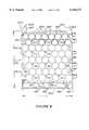
- the assemblyis created in a network of channels in surface 2658 consisting of center channel 2662, intermediate circumferential channel 2664 and outer circumferential channel 2666. Channels 2664 and 2666 are configured as concentric closed loops or ovals surrounding center channel 2662.
- target utilization in sputtering operationsare about 15-20% for nonmagnetic materials and about 30-35% for magnetic materials.
- optimal target utilizationis another prime concern in sputtering operations.
- Magnet and magnetic pole piece assemblies used in the present inventionsubstantially improve target utilization, enhancing both production throughputs and cost-effectiveness.
- FIGS. 27A and 27Billustrate in greater detail the magnet and magnetic pole piece assemblies for nonmagnetic (e.g., chromium and carbon) and magnetic (e.g., CoCrTa) targets, respectively.
- Each magnet 2768is 1-inch long by 5/16-inch wide by 3/16-inch thick and magnets 2769 are 1-inch-long by 5/16-inch wide by 3/8-inch thick, with north and south pole directions indicated by arrows pointing up and down, respectively.
- Ferritic magnets of neodymium, iron and boronare preferred in the present invention.
- magnetic pole pieces 2770 and 2774are arrayed in channels 2662, 2664 and 2666. Magnetic pole pieces 2770 may be adapted to receive screws therethrough for securing the magnet and pole piece assembly within the channels as necessary.
- a nonmagnetic material 2772such as aluminum in block or continuous form, is positioned so as to fill the channels as necessary and preclude shunting of the magnetic flux between adjacent magnetic pole pieces 2770.
- Iron plate 2274serves as a backing plate for the magnetic and pole piece assembly.
- center channel 2662 of each cathodecontains about 25 magnets 2769 separated by 1/4-inch spaces and 25-inch pole piece strips 2770 above and below magnets 2769.
- Intermediate circumferential channel 2664contains about 35 magnets 2768 separated by 1-inch spaces, two 31-inch pole piece strips 2770, two 31-inch pole piece strips 2774 adjacent to aluminum filler 2772 with additional pole pieces 2770 for fitting the cropped corners of intermediate channel 2664.
- Outer circumferential 2666contains about 33 magnets 2769 and two 33-inch pole piece strips 2770 with additional pole pieces 2770 for fitting the cropped corners of outer circumferential channel 2666.
- the overall effect of the magnet and the pole piece assembly for the nonmagnetic target shown in FIG. 27Ais to produce a magnetic field strength above the target surface of 400 Gauss at the center of the erosion region.
- center channel 2662contains about 25 magnets 2769 with one overlying 25-inch pole piece 2770.
- Intermediate circumferential channel 2664contains about 35 magnets 2768 overlaid with two 31-inch pole pieces 2770 and additional pole pieces 2770 for fitting the cropped corners of intermediate channel 2664.
- Aluminum filler material 2772in block or continuous form, occupies remaining vacancies in intermediate channel 2664.
- the overall effect of the magnet and pole piece assembly for a magnetic target shown in FIG. 27Bis to produce a magnetic field strength of about 400 Gauss at the center of the erosion region.
- the purpose of the magnetic fieldis to trap electrons and ionized species in the plasma and enhance the sputtering rate induced by the circulating plasma above the target surface.
- the magnetic field 2700 generated by the magnet and magnetic pole piece assemblies used in the present inventionapproximate an ideal magnetic field 2700 where the vertical components of the magnetic fields above the nonmagnetic (FIG. 27A) and magnetic (FIG. 27B) targets are reduced. As a result, greater target utilization is obtained since the magnetic fields and plasma are focused across a relatively greater portion of the target surface.
- Target utilizationmay be further improved by increasing the magnet loading density within the channel network. For example, by loading intermediate channel 2664 with 24 magnets 2768 separated by 1/2-inch spaces, nonmagnetic target utilization increases to between 50% and 65%. For magnetic targets, an increased utilization of between 35% to 50% may result.
- FIG. 28illustrates the film structure which may be produced by the present invention on nickel-phosphorus plated aluminum disk substrate 510.
- a 800 ⁇ to 2000 ⁇ (1000 ⁇ preferably) chromium underlayer 2800is deposited first on disk substrate 510.
- a 500 ⁇ to 850 ⁇ CoCrTa magnetic layer 2802may be deposited over the chromium underlayer.
- the ⁇ C ⁇ axis of the hcp structure of the magnetic cobalt alloyis aligned in the film plane.
- a 350 ⁇ carbon overlayer 2804may be deposited, incorporating some hydrogen, as discussed in Section J.
- Sputtering chamber design in sputtering apparatus 10 for carbon filmsrequires additional refinements to optimize wear and corrosion resistance properties. These refinements are discussed herein with reference to FIG. 13, as necessary.
- a second type of chamber refinement in the carbon sputtering chamberrelates to the need for substrate bias.
- primary or "fast" electronsdislodge from the target and join the plasma. These fast electrons are constrained to field lines in the plasma where they may ionize argon atoms or may be attracted to positively biased regions within the sputtering chamber.
- Deposition of dielectric target materials, such as carbon, on surfaces other than the substratecan reduce the electrical conductivity of those surfaces and inhibit the electron grounding thereon.
- cryo pump C3to 10 -5 Torr.
- the palletproceeds at 6 ft/min past heat reflective panels 2120.
- Pallet 800enters chromium sputtering chamber 20 maintained at 9-12 microns (9-12 mTorr) of argon pressure with argon flow at 300 standard cubic centimeters per minute (sccm). Pallet 800 travels at 6 ft/min as it passes sputtering targets 2226-2229.
- the sputtering poweris 7.5 kW per cathode, with a 1,000 ⁇ thick chromium film deposited.
- Transport speed through dwell chamber 22A, buffer chamber 24A and dwell chamber 22Bis 12 ft/min through open doors D5 and D6. These three chambers are pumped by cryo pumps C4, C5, and C6.
- Pallet 800enters magnetic sputtering chamber 26 maintained at 9-12 microns [9-12 mTorr) of argon by cryo pumps C6 and C7 with argon flow at approximately 400 sccm.
- the transport speed through sputtering chamber 26is 6 ft/min.
- the sputtering poweris 7.5 kW per cathode, depositing a 800 ⁇ thick CoCrTa film.
- Transport speed through dwell chambers 22C and 22D and buffer chamber 24Bis 6 ft/min.
- Dwell chambers 22C, 22D and buffer chamber 24Bare pumped by cryo pumps C7, C8 and C9.
- Pallet 800enters carbon sputtering chamber 28 maintained at 9-10 microns (9-12 mTorr) by cryo pumps C9 and C10 with argon and up to 15% hydrocarbon gas like ethylene or acetylene flowing at 100 sccm.
- the transport speedis 2.8 ft/min as the pallet passes the sputtering targets in carbon sputtering chamber 28.
- Sputtering poweris 7 kW per cathode with a film thickness of 350 ⁇ .
- Transport speed through dwell chamber 22E, buffer chamber 24C and exit buffer chamber 29is 6 ft/min with doors D9 and D10 opening and closing sequentially to allow pallet 800 to proceed.
- Dwell chamber 22Eis pumped by cryo pumps C10 and C11, buffer chamber 24C and exit buffer chamber 29 are pumped by cryo pump C12. Argon is backfilled into exit buffer chamber 29 by cryo pump C12 to equalize the pressure differential existing with respect to exit lock chamber 30.
- Pallet 800next proceeds through exit lock chamber 30 which is vented to the atmosphere by chamber vent valve CV5 in 10 seconds. Pallet 800 then proceeds to robotic unloading station 45.
- the soak time in dwell heating chamber 14may be increased to about 50 seconds to allow the substrate temperature to increase to approximately 250° C. and/or the pallet transport speed through chromium sputtering chamber 20 may be reduced in order to allow a thicker deposition of a chromium underlayer. Adjustment of soak time and/or substrate temperature parameters depends on the life cycle of the pallet--a pallet which has proceeded through numerous sputtering runs will have a thicker film deposition which can absorb more water and consequently would have more water to outgas before film deposition.
- such an apparatus and processis achieved through a novel combination of process and structural elements involved in disk preparation, provision of a sputtering environment, transportation of substrates through the sputtering environment at rapid speeds and in a contaminant free manner, heating the substrates to optimal thermal levels for sputtering, and sputtering the substrates through a series of substantially isolated, non-crosscontaminating sputtering steps.
- the apparatus of the present inventionprovides a high-speed in-line sputtering apparatus for producing superior multilayer films on substrates, such as disks suitable for use in Winchester-type hard disk drives.
- the process of the present inventionprovides an improved method of providing multilayer coatings to a variety of substrate types at a much greater rate than prior art methods.
- a novel means for heating substrates to be coateda novel sputtering magnetron design, a novel, variable speed, overhead, non-contaminating substrate transportation system and a comprehensive, centralized, programmable electronic means for controlling the apparatus and process are provided. Still further, when she process and apparatus are used for providing magnetic coatings for substrates, such as disks, to be utilized in hard disk drives using Winchester-type technology, a unique disk texturing method for improving the disk's magnetic recording properties, and a novel disk carrier (or pallet) design which contributes to uniform substrate heating characteristics in a large, single, high capacity pallet, are also provided herein. Numerous variations are possible as will be apparent to those skilled in the art; such variations are intended to be within the scope of the invention as defined by this specification and the following claims are intended to cover all the modifications and equivalents falling within the scope of the invention.
Landscapes
- Engineering & Computer Science (AREA)
- Chemical & Material Sciences (AREA)
- Physics & Mathematics (AREA)
- General Physics & Mathematics (AREA)
- Manufacturing & Machinery (AREA)
- Power Engineering (AREA)
- Condensed Matter Physics & Semiconductors (AREA)
- Computer Hardware Design (AREA)
- Microelectronics & Electronic Packaging (AREA)
- Mechanical Engineering (AREA)
- Metallurgy (AREA)
- Organic Chemistry (AREA)
- Chemical Kinetics & Catalysis (AREA)
- Materials Engineering (AREA)
- Automation & Control Theory (AREA)
- Analytical Chemistry (AREA)
- Plasma & Fusion (AREA)
- General Engineering & Computer Science (AREA)
- Quality & Reliability (AREA)
- Physical Vapour Deposition (AREA)
- Manufacturing Of Magnetic Record Carriers (AREA)
Abstract
Description
Claims (7)
Priority Applications (1)
| Application Number | Priority Date | Filing Date | Title |
|---|---|---|---|
| US08/045,989US6156171A (en) | 1991-04-04 | 1993-04-09 | Sputtering magnetron |
Applications Claiming Priority (2)
| Application Number | Priority Date | Filing Date | Title |
|---|---|---|---|
| US68186691A | 1991-04-04 | 1991-04-04 | |
| US08/045,989US6156171A (en) | 1991-04-04 | 1993-04-09 | Sputtering magnetron |
Related Parent Applications (1)
| Application Number | Title | Priority Date | Filing Date |
|---|---|---|---|
| US68186691ADivision | 1991-04-04 | 1991-04-04 |
Publications (1)
| Publication Number | Publication Date |
|---|---|
| US6156171Atrue US6156171A (en) | 2000-12-05 |
Family
ID=24737182
Family Applications (4)
| Application Number | Title | Priority Date | Filing Date |
|---|---|---|---|
| US08/046,215Expired - LifetimeUS5814196A (en) | 1991-04-04 | 1993-04-08 | Apparatus and method for high throughput sputtering |
| US08/045,975Expired - LifetimeUS5972184A (en) | 1991-04-04 | 1993-04-09 | Heating system for high throughput sputtering |
| US08/045,989Expired - LifetimeUS6156171A (en) | 1991-04-04 | 1993-04-09 | Sputtering magnetron |
| US08/552,250Expired - LifetimeUS5683561A (en) | 1991-04-04 | 1995-11-02 | Apparatus and method for high throughput sputtering |
Family Applications Before (2)
| Application Number | Title | Priority Date | Filing Date |
|---|---|---|---|
| US08/046,215Expired - LifetimeUS5814196A (en) | 1991-04-04 | 1993-04-08 | Apparatus and method for high throughput sputtering |
| US08/045,975Expired - LifetimeUS5972184A (en) | 1991-04-04 | 1993-04-09 | Heating system for high throughput sputtering |
Family Applications After (1)
| Application Number | Title | Priority Date | Filing Date |
|---|---|---|---|
| US08/552,250Expired - LifetimeUS5683561A (en) | 1991-04-04 | 1995-11-02 | Apparatus and method for high throughput sputtering |
Country Status (5)
| Country | Link |
|---|---|
| US (4) | US5814196A (en) |
| EP (1) | EP0577766B1 (en) |
| JP (1) | JP3416910B2 (en) |
| DE (1) | DE69230493T2 (en) |
| WO (1) | WO1992017621A1 (en) |
Cited By (32)
| Publication number | Priority date | Publication date | Assignee | Title |
|---|---|---|---|---|
| US20030059623A1 (en)* | 2000-09-11 | 2003-03-27 | O'shaughnessy Roger D | Temporary protective covers |
| US20030118860A1 (en)* | 2001-09-11 | 2003-06-26 | O'shaughnessy Roger D. | Hydrophilic surfaces carrying temporary protective covers |
| US20030150712A1 (en)* | 2002-02-13 | 2003-08-14 | Reiter Jeffrey Shane | System and method for controlling thin film defects |
| US6660365B1 (en) | 1998-12-21 | 2003-12-09 | Cardinal Cg Company | Soil-resistant coating for glass surfaces |
| WO2003003417A3 (en)* | 2001-06-29 | 2004-02-26 | Plasmion Corp | High throughput hybrid deposition system and method using the same |
| US20040069614A1 (en)* | 2002-08-02 | 2004-04-15 | Mcleod Paul Stephen | Timing apparatus and method to selectively bias during sputtering |
| US6886244B1 (en) | 2002-02-25 | 2005-05-03 | Seagate Technology Llc | Segmented pallet for disk-shaped substrate electrical biassing and apparatus comprising same |
| US6964731B1 (en) | 1998-12-21 | 2005-11-15 | Cardinal Cg Company | Soil-resistant coating for glass surfaces |
| US20050252766A1 (en)* | 2004-05-12 | 2005-11-17 | Greenberg Thomas L | Cathode apparatus to selectively bias pallet during sputtering |
| US6974629B1 (en) | 1999-08-06 | 2005-12-13 | Cardinal Cg Company | Low-emissivity, soil-resistant coating for glass surfaces |
| US20060021576A1 (en)* | 2004-08-02 | 2006-02-02 | Seagate Technology Llc. | Multi-chamber processing with simultaneous workpiece transport and gas delivery |
| US20060196414A1 (en)* | 2005-03-03 | 2006-09-07 | Applied Films Gmbh & Co., Kg | System for coating a substrate, and an insert element |
| EP1826292A1 (en)* | 2006-02-23 | 2007-08-29 | Bekaert Advanced Coatings | Sputter module. |
| KR100765997B1 (en)* | 2001-08-21 | 2007-10-11 | 삼성코닝 주식회사 | Inline sputtering system |
| US7294404B2 (en) | 2003-12-22 | 2007-11-13 | Cardinal Cg Company | Graded photocatalytic coatings |
| US20080017501A1 (en)* | 2006-07-21 | 2008-01-24 | Makoto Inagawa | Cooled dark space shield for multi-cathode design |
| US20080213071A1 (en)* | 2007-02-09 | 2008-09-04 | Applied Materials, Inc. | Transport device in an installation for the treatment of substrates |
| US7604865B2 (en) | 2004-07-12 | 2009-10-20 | Cardinal Cg Company | Low-maintenance coatings |
| US20110056908A1 (en)* | 2008-05-13 | 2011-03-10 | Showa Denko K.K. | Method and apparatus for manufacturing magnetic recording medium |
| US7923114B2 (en) | 2004-12-03 | 2011-04-12 | Cardinal Cg Company | Hydrophilic coatings, methods for depositing hydrophilic coatings, and improved deposition technology for thin films |
| US7989094B2 (en) | 2006-04-19 | 2011-08-02 | Cardinal Cg Company | Opposed functional coatings having comparable single surface reflectances |
| US8092660B2 (en) | 2004-12-03 | 2012-01-10 | Cardinal Cg Company | Methods and equipment for depositing hydrophilic coatings, and deposition technologies for thin films |
| US8432603B2 (en) | 2009-03-31 | 2013-04-30 | View, Inc. | Electrochromic devices |
| US20130187546A1 (en)* | 2012-01-20 | 2013-07-25 | Taiwan Semiconductor Manufacturing Co., Ltd. | Novel Coherent Multiple Side Electromagnets |
| US8506768B2 (en) | 2007-09-14 | 2013-08-13 | Cardinal Cg Company | Low-maintenance coatings, and methods for producing low-maintenance coatings |
| US9454053B2 (en) | 2011-12-12 | 2016-09-27 | View, Inc. | Thin-film devices and fabrication |
| US9738967B2 (en) | 2006-07-12 | 2017-08-22 | Cardinal Cg Company | Sputtering apparatus including target mounting and control |
| US9782949B2 (en) | 2008-05-30 | 2017-10-10 | Corning Incorporated | Glass laminated articles and layered articles |
| US9856557B1 (en) | 2016-01-22 | 2018-01-02 | Seagate Technology Llc | Fabrication of a multi-layered magnetic element |
| US10273573B2 (en) | 2015-12-11 | 2019-04-30 | Cardinal Cg Company | Method of coating both sides of a substrate using a sacrificial coating |
| US10604442B2 (en) | 2016-11-17 | 2020-03-31 | Cardinal Cg Company | Static-dissipative coating technology |
| TWI860206B (en)* | 2022-02-15 | 2024-10-21 | 美商因特瓦克公司 | A linear sputtering system for making thick-multilayer dielectric films |
Families Citing this family (323)
| Publication number | Priority date | Publication date | Assignee | Title |
|---|---|---|---|---|
| US5831851A (en) | 1995-03-21 | 1998-11-03 | Seagate Technology, Inc. | Apparatus and method for controlling high throughput sputtering |
| US5660114A (en)* | 1995-05-10 | 1997-08-26 | Seagate Technology, Inc. | Transport system for thin film sputtering system |
| US5705044A (en)* | 1995-08-07 | 1998-01-06 | Akashic Memories Corporation | Modular sputtering machine having batch processing and serial thin film sputtering |
| JPH09172001A (en)* | 1995-12-15 | 1997-06-30 | Sony Corp | Method and device for controlling temperature in semiconductor manufacturing apparatus |
| US5670030A (en)* | 1996-03-19 | 1997-09-23 | Optical Coating Laboratory, Inc. | Methods for preparing low scatter optical coatings |
| US5753092A (en)* | 1996-08-26 | 1998-05-19 | Velocidata, Inc. | Cylindrical carriage sputtering system |
| US6656329B1 (en) | 1996-08-28 | 2003-12-02 | Premark Rwp Holdings, Inc. | Coated pressing surfaces for abrasion resistant laminate and making laminates therefrom |
| IT1290911B1 (en)* | 1997-02-03 | 1998-12-14 | Siv Soc Italiana Vetro | PROCEDURE AND DEVICE FOR THE POWER SUPPLY OF VACUUM SYSTEMS SUITABLE FOR THE DEPOSIT OF SURFACE COVERINGS ON SUBSTRATES. |
| US6432203B1 (en)* | 1997-03-17 | 2002-08-13 | Applied Komatsu Technology, Inc. | Heated and cooled vacuum chamber shield |
| JP3468056B2 (en)* | 1997-09-23 | 2003-11-17 | 東京エレクトロン株式会社 | Substrate detection device |
| US6190514B1 (en)* | 1997-12-30 | 2001-02-20 | Premark Rwp Holdings, Inc. | Method for high scan sputter coating to produce coated, abrasion resistant press plates with reduced built-in thermal stress |
| US6086362A (en)* | 1998-05-20 | 2000-07-11 | Applied Komatsu Technology, Inc. | Multi-function chamber for a substrate processing system |
| US6215897B1 (en) | 1998-05-20 | 2001-04-10 | Applied Komatsu Technology, Inc. | Automated substrate processing system |
| US6482301B1 (en) | 1998-06-04 | 2002-11-19 | Seagate Technology, Inc. | Target shields for improved magnetic properties of a recording medium |
| ATE236861T1 (en)* | 1998-12-21 | 2003-04-15 | Cardinal Cg Co | DIRT-RESISTANT COATING FOR GLASS SURFACES |
| US6948113B1 (en) | 1999-04-21 | 2005-09-20 | Seagate Technology Llc | Self-throttling error-correction buffer and method for a disc drive |
| US6424880B1 (en) | 1999-09-10 | 2002-07-23 | Applied Materials, Inc. | Multi-computer chamber control system, method and medium |
| US6949143B1 (en) | 1999-12-15 | 2005-09-27 | Applied Materials, Inc. | Dual substrate loadlock process equipment |
| US6592709B1 (en)* | 2000-04-05 | 2003-07-15 | Applied Materials Inc. | Method and apparatus for plasma processing |
| US6372098B1 (en)* | 2000-09-28 | 2002-04-16 | The Boc Group, Inc. | High target utilization magnet array and associated methods |
| US6599368B1 (en) | 2000-10-05 | 2003-07-29 | Applied Materials, Inc. | System architecture of semiconductor manufacturing equipment |
| US6558750B2 (en) | 2001-07-16 | 2003-05-06 | Technic Inc. | Method of processing and plating planar articles |
| US6524463B2 (en) | 2001-07-16 | 2003-02-25 | Technic, Inc. | Method of processing wafers and other planar articles within a processing cell |
| US7799731B2 (en)* | 2001-09-28 | 2010-09-21 | Shibaura Mechatronics Corporation | Photocatalyst element, method and device for preparing the same |
| US6808741B1 (en)* | 2001-10-26 | 2004-10-26 | Seagate Technology Llc | In-line, pass-by method for vapor lubrication |
| JP2003196821A (en)* | 2001-12-25 | 2003-07-11 | Fuji Electric Co Ltd | Magnetic recording medium, method of manufacturing the same, and magnetic recording apparatus |
| US6843892B1 (en) | 2002-02-19 | 2005-01-18 | Seagate Technology Llc | Apparatus and method for selectively and controllably electrically biasing a plurality of substrates on a pallet |
| US6749729B1 (en)* | 2002-03-13 | 2004-06-15 | Seagate Technology Llc | Method and apparatus for workpiece biassing utilizing non-arcing bias rail |
| KR20050012804A (en)* | 2002-06-19 | 2005-02-02 | 토소우 에스엠디, 인크 | Sputter target monitoring system |
| JP4033126B2 (en)* | 2003-02-20 | 2008-01-16 | セイコーエプソン株式会社 | Fuel cell manufacturing apparatus and fuel cell manufacturing method |
| US20050221603A1 (en)* | 2003-06-23 | 2005-10-06 | Applied Materials, Inc. | System architecture of semiconductor manufacturing equipment |
| KR100500169B1 (en)* | 2003-07-02 | 2005-07-07 | 주식회사 디엠에스 | Docking-type system for transporting and treating works and the method of the same |
| DE102004006419A1 (en)* | 2004-02-09 | 2005-09-08 | Applied Films Gmbh & Co. Kg | Energy and media connection for a multi-chamber coating system |
| US7837836B2 (en)* | 2004-02-12 | 2010-11-23 | Seagate Technology Llc | Method and apparatus for multi-stage sputter deposition of uniform thickness layers |
| US7678198B2 (en)* | 2004-08-12 | 2010-03-16 | Cardinal Cg Company | Vertical-offset coater |
| WO2006080968A2 (en) | 2004-11-15 | 2006-08-03 | Cardinal Cg Company | Methods and equipment for depositing coatings having sequenced structures |
| KR101213849B1 (en)* | 2005-12-16 | 2012-12-18 | 엘지디스플레이 주식회사 | Sputtering apparatus |
| JP4843535B2 (en)* | 2007-03-19 | 2011-12-21 | 昭和電工株式会社 | Laminated film forming system, sputtering apparatus, and laminated film forming method |
| US8557093B2 (en) | 2007-03-22 | 2013-10-15 | Sunpower Corporation | Deposition system with electrically isolated pallet and anode assemblies |
| DE102007023970A1 (en)* | 2007-05-23 | 2008-12-04 | Aixtron Ag | Apparatus for coating a plurality of densely packed substrates on a susceptor |
| TWI396763B (en)* | 2007-06-01 | 2013-05-21 | Hon Hai Prec Ind Co Ltd | Satge for sputtering and sputtering apparatus using same |
| US8096539B2 (en) | 2007-06-28 | 2012-01-17 | Hitachi Global Storage Technologies, Netherlands, B.V. | O-ring free cooling pallet for hard disk drive slider carriers |
| BE1017852A3 (en)* | 2007-11-19 | 2009-09-01 | Ind Plasma Services & Technologies Ipst Gmbh | METHOD AND INSTALLATION OF GALVANIZATION BY PLASMA EVAPORATION |
| US9175383B2 (en)* | 2008-01-16 | 2015-11-03 | Applied Materials, Inc. | Double-coating device with one process chamber |
| US8208238B1 (en)* | 2008-03-21 | 2012-06-26 | Seagate Technology, Llc | Apparatus for orienting soft-underlayer deposition |
| US20090255808A1 (en)* | 2008-04-11 | 2009-10-15 | Seagate Technology Llc | Target for efficient use of precious deposition material |
| US20100006420A1 (en)* | 2008-07-08 | 2010-01-14 | Seagate Technology Llc | Inline interlayer heater apparatus |
| JP2010027157A (en)* | 2008-07-22 | 2010-02-04 | Ulvac Japan Ltd | Magnetic recording medium manufacturing system |
| US20100101937A1 (en)* | 2008-10-29 | 2010-04-29 | Applied Vacuum Coating Technologies Co., Ltd. | Method of fabricating transparent conductive film |
| US8842357B2 (en) | 2008-12-31 | 2014-09-23 | View, Inc. | Electrochromic device and method for making electrochromic device |
| US9051650B2 (en)* | 2009-01-16 | 2015-06-09 | Marca Machinery, Llc | In-line metallizer assemblies and part-coating conveyor systems incorporating the same |
| US9685186B2 (en)* | 2009-02-27 | 2017-06-20 | Applied Materials, Inc. | HDD pattern implant system |
| US10026436B2 (en)* | 2009-07-01 | 2018-07-17 | Nordson Corporation | Apparatus and methods for supporting workpieces during plasma processing |
| US8406918B2 (en)* | 2009-12-21 | 2013-03-26 | WD Media, LLC | Master teaching jig |
| JP5649426B2 (en)* | 2009-12-22 | 2015-01-07 | キヤノンアネルバ株式会社 | Sputtering apparatus, sputtering film forming method, and sputtering apparatus power control method |
| TW201124548A (en)* | 2010-01-11 | 2011-07-16 | Hon Hai Prec Ind Co Ltd | Sputtering device |
| US10550474B1 (en)* | 2010-02-26 | 2020-02-04 | Quantum Innovations, Inc. | Vapor deposition system |
| KR101796656B1 (en)* | 2010-04-30 | 2017-11-13 | 어플라이드 머티어리얼스, 인코포레이티드 | Vertical inline cvd system |
| US9156204B2 (en) | 2010-05-17 | 2015-10-13 | Synerdyne Corporation | Hybrid scanner fabricator |
| US8905742B2 (en) | 2010-09-17 | 2014-12-09 | Synerdyne Corporation | Compact rotary platen 3D printer |
| US8479795B2 (en)* | 2010-09-17 | 2013-07-09 | Synerdyne Corporation | System and method for rapid fabrication of arbitrary three-dimensional objects |
| TW201213572A (en)* | 2010-09-29 | 2012-04-01 | Hon Hai Prec Ind Co Ltd | Sputtering apparatus |
| DE102010054483A1 (en)* | 2010-12-14 | 2012-06-14 | Manz Automation Ag | Mobile, portable electrostatic substrate holder assembly |
| JP5602005B2 (en)* | 2010-12-22 | 2014-10-08 | キヤノンアネルバ株式会社 | Vacuum processing apparatus and processing method using the same |
| EP2689050A2 (en)* | 2011-03-25 | 2014-01-29 | LG Electronics Inc. | Plasma enhanced chemical vapor deposition apparatus and method for controlling the same |
| US20120247953A1 (en)* | 2011-03-28 | 2012-10-04 | Chien-Min Weng | Film-coating system |
| CN102828149A (en)* | 2011-06-13 | 2012-12-19 | 鸿富锦精密工业(深圳)有限公司 | Film-coating member and manufacturing method thereof |
| US20130023129A1 (en) | 2011-07-20 | 2013-01-24 | Asm America, Inc. | Pressure transmitter for a semiconductor processing environment |
| CN102347233B (en)* | 2011-08-14 | 2013-11-06 | 上海合晶硅材料有限公司 | Method and tray for improving thickness evenness of silicon wafer in process of backlining the silicon wafer |
| US20130143415A1 (en)* | 2011-12-01 | 2013-06-06 | Applied Materials, Inc. | Multi-Component Film Deposition |
| JP6205368B2 (en)* | 2011-12-27 | 2017-09-27 | インテヴァック インコーポレイテッド | System configuration for combined static and pass-by processing |
| JP6060484B2 (en)* | 2012-01-19 | 2017-01-18 | 富士電機株式会社 | Method for manufacturing magnetic recording medium |
| EP2650135A1 (en) | 2012-04-12 | 2013-10-16 | KBA-NotaSys SA | Intaglio printing plate coating apparatus |
| US20160376700A1 (en) | 2013-02-01 | 2016-12-29 | Asm Ip Holding B.V. | System for treatment of deposition reactor |
| CN103173744A (en)* | 2013-04-12 | 2013-06-26 | 光垒光电科技(上海)有限公司 | Tray and reaction chamber including same |
| US11688589B2 (en) | 2013-06-10 | 2023-06-27 | View, Inc. | Carrier with vertical grid for supporting substrates in coater |
| EP3008224B1 (en)* | 2013-06-10 | 2024-09-04 | View, Inc. | Glass pallet for sputtering systems |
| US20150021163A1 (en)* | 2013-07-16 | 2015-01-22 | Tsmc Solar Ltd. | Apparatus and method for producing solar cells with a heater apparatus |
| WO2015026445A1 (en)* | 2013-08-21 | 2015-02-26 | Applied Materials, Inc. | Variable frequency microwave (vfm) processes and applications in semiconductor thin film fabrications |
| TWI600792B (en)* | 2013-11-26 | 2017-10-01 | 應用材料股份有限公司 | Apparatus for reducing the effect of contamination on a rapid thermal process |
| US10941490B2 (en) | 2014-10-07 | 2021-03-09 | Asm Ip Holding B.V. | Multiple temperature range susceptor, assembly, reactor and system including the susceptor, and methods of using the same |
| US10276355B2 (en) | 2015-03-12 | 2019-04-30 | Asm Ip Holding B.V. | Multi-zone reactor, system including the reactor, and method of using the same |
| US20180258519A1 (en)* | 2015-10-25 | 2018-09-13 | Applied Materials, Inc. | Apparatus for vacuum deposition on a substrate and method for masking the substrate during vacuum deposition |
| US11139308B2 (en) | 2015-12-29 | 2021-10-05 | Asm Ip Holding B.V. | Atomic layer deposition of III-V compounds to form V-NAND devices |
| EP4219786A3 (en) | 2016-02-09 | 2023-10-11 | Wilsonart LLC | Method for coating stainless steel press plates and coated press plates produced thereby |
| US10529554B2 (en) | 2016-02-19 | 2020-01-07 | Asm Ip Holding B.V. | Method for forming silicon nitride film selectively on sidewalls or flat surfaces of trenches |
| US10343920B2 (en) | 2016-03-18 | 2019-07-09 | Asm Ip Holding B.V. | Aligned carbon nanotubes |
| US11453943B2 (en) | 2016-05-25 | 2022-09-27 | Asm Ip Holding B.V. | Method for forming carbon-containing silicon/metal oxide or nitride film by ALD using silicon precursor and hydrocarbon precursor |
| US10612137B2 (en) | 2016-07-08 | 2020-04-07 | Asm Ip Holdings B.V. | Organic reactants for atomic layer deposition |
| US9859151B1 (en) | 2016-07-08 | 2018-01-02 | Asm Ip Holding B.V. | Selective film deposition method to form air gaps |
| US9812320B1 (en) | 2016-07-28 | 2017-11-07 | Asm Ip Holding B.V. | Method and apparatus for filling a gap |
| US9887082B1 (en) | 2016-07-28 | 2018-02-06 | Asm Ip Holding B.V. | Method and apparatus for filling a gap |
| US11532757B2 (en) | 2016-10-27 | 2022-12-20 | Asm Ip Holding B.V. | Deposition of charge trapping layers |
| US10714350B2 (en) | 2016-11-01 | 2020-07-14 | ASM IP Holdings, B.V. | Methods for forming a transition metal niobium nitride film on a substrate by atomic layer deposition and related semiconductor device structures |
| KR102546317B1 (en) | 2016-11-15 | 2023-06-21 | 에이에스엠 아이피 홀딩 비.브이. | Gas supply unit and substrate processing apparatus including the same |
| US11447861B2 (en) | 2016-12-15 | 2022-09-20 | Asm Ip Holding B.V. | Sequential infiltration synthesis apparatus and a method of forming a patterned structure |
| US11581186B2 (en) | 2016-12-15 | 2023-02-14 | Asm Ip Holding B.V. | Sequential infiltration synthesis apparatus |
| US11390950B2 (en) | 2017-01-10 | 2022-07-19 | Asm Ip Holding B.V. | Reactor system and method to reduce residue buildup during a film deposition process |
| US10468261B2 (en) | 2017-02-15 | 2019-11-05 | Asm Ip Holding B.V. | Methods for forming a metallic film on a substrate by cyclical deposition and related semiconductor device structures |
| US10954598B2 (en) | 2017-02-28 | 2021-03-23 | George Xinsheng Guo | High throughput vacuum deposition sources and system |
| DE102017106373A1 (en)* | 2017-03-24 | 2018-09-27 | Nexwafe Gmbh | Process chamber guide, process chamber and method for guiding a substrate carrier to a process position |
| US10770286B2 (en) | 2017-05-08 | 2020-09-08 | Asm Ip Holdings B.V. | Methods for selectively forming a silicon nitride film on a substrate and related semiconductor device structures |
| US12040200B2 (en) | 2017-06-20 | 2024-07-16 | Asm Ip Holding B.V. | Semiconductor processing apparatus and methods for calibrating a semiconductor processing apparatus |
| US11306395B2 (en) | 2017-06-28 | 2022-04-19 | Asm Ip Holding B.V. | Methods for depositing a transition metal nitride film on a substrate by atomic layer deposition and related deposition apparatus |
| KR20190009245A (en) | 2017-07-18 | 2019-01-28 | 에이에스엠 아이피 홀딩 비.브이. | Methods for forming a semiconductor device structure and related semiconductor device structures |
| US11374112B2 (en) | 2017-07-19 | 2022-06-28 | Asm Ip Holding B.V. | Method for depositing a group IV semiconductor and related semiconductor device structures |
| US10590535B2 (en) | 2017-07-26 | 2020-03-17 | Asm Ip Holdings B.V. | Chemical treatment, deposition and/or infiltration apparatus and method for using the same |
| TWI815813B (en) | 2017-08-04 | 2023-09-21 | 荷蘭商Asm智慧財產控股公司 | Showerhead assembly for distributing a gas within a reaction chamber |
| US10692741B2 (en) | 2017-08-08 | 2020-06-23 | Asm Ip Holdings B.V. | Radiation shield |
| US10770336B2 (en) | 2017-08-08 | 2020-09-08 | Asm Ip Holding B.V. | Substrate lift mechanism and reactor including same |
| US11769682B2 (en) | 2017-08-09 | 2023-09-26 | Asm Ip Holding B.V. | Storage apparatus for storing cassettes for substrates and processing apparatus equipped therewith |
| US11830730B2 (en) | 2017-08-29 | 2023-11-28 | Asm Ip Holding B.V. | Layer forming method and apparatus |
| US11295980B2 (en) | 2017-08-30 | 2022-04-05 | Asm Ip Holding B.V. | Methods for depositing a molybdenum metal film over a dielectric surface of a substrate by a cyclical deposition process and related semiconductor device structures |
| US10658205B2 (en) | 2017-09-28 | 2020-05-19 | Asm Ip Holdings B.V. | Chemical dispensing apparatus and methods for dispensing a chemical to a reaction chamber |
| US10403504B2 (en) | 2017-10-05 | 2019-09-03 | Asm Ip Holding B.V. | Method for selectively depositing a metallic film on a substrate |
| US10923344B2 (en) | 2017-10-30 | 2021-02-16 | Asm Ip Holding B.V. | Methods for forming a semiconductor structure and related semiconductor structures |
| CN111344522B (en) | 2017-11-27 | 2022-04-12 | 阿斯莫Ip控股公司 | Including clean mini-environment device |
| WO2019103613A1 (en) | 2017-11-27 | 2019-05-31 | Asm Ip Holding B.V. | A storage device for storing wafer cassettes for use with a batch furnace |
| US20190195547A1 (en)* | 2017-12-27 | 2019-06-27 | William G. Moon | Modular and separable cryogenic shipping system |
| US10872771B2 (en) | 2018-01-16 | 2020-12-22 | Asm Ip Holding B. V. | Method for depositing a material film on a substrate within a reaction chamber by a cyclical deposition process and related device structures |
| KR102695659B1 (en) | 2018-01-19 | 2024-08-14 | 에이에스엠 아이피 홀딩 비.브이. | Method for depositing a gap filling layer by plasma assisted deposition |
| TWI799494B (en) | 2018-01-19 | 2023-04-21 | 荷蘭商Asm 智慧財產控股公司 | Deposition method |
| US11081345B2 (en) | 2018-02-06 | 2021-08-03 | Asm Ip Holding B.V. | Method of post-deposition treatment for silicon oxide film |
| US11056722B2 (en)* | 2018-02-08 | 2021-07-06 | International Business Machines Corporation | Tool and method of fabricating a self-aligned solid state thin film battery |
| US10679853B2 (en) | 2018-02-08 | 2020-06-09 | International Business Machines Corporation | Self-aligned, over etched hard mask fabrication method and structure |
| US10896820B2 (en) | 2018-02-14 | 2021-01-19 | Asm Ip Holding B.V. | Method for depositing a ruthenium-containing film on a substrate by a cyclical deposition process |
| WO2019158960A1 (en) | 2018-02-14 | 2019-08-22 | Asm Ip Holding B.V. | A method for depositing a ruthenium-containing film on a substrate by a cyclical deposition process |
| US10731249B2 (en) | 2018-02-15 | 2020-08-04 | Asm Ip Holding B.V. | Method of forming a transition metal containing film on a substrate by a cyclical deposition process, a method for supplying a transition metal halide compound to a reaction chamber, and related vapor deposition apparatus |
| KR102636427B1 (en) | 2018-02-20 | 2024-02-13 | 에이에스엠 아이피 홀딩 비.브이. | Substrate processing method and apparatus |
| US10975470B2 (en) | 2018-02-23 | 2021-04-13 | Asm Ip Holding B.V. | Apparatus for detecting or monitoring for a chemical precursor in a high temperature environment |
| US11473195B2 (en) | 2018-03-01 | 2022-10-18 | Asm Ip Holding B.V. | Semiconductor processing apparatus and a method for processing a substrate |
| KR102646467B1 (en) | 2018-03-27 | 2024-03-11 | 에이에스엠 아이피 홀딩 비.브이. | Method of forming an electrode on a substrate and a semiconductor device structure including an electrode |
| KR102600229B1 (en) | 2018-04-09 | 2023-11-10 | 에이에스엠 아이피 홀딩 비.브이. | Substrate supporting device, substrate processing apparatus including the same and substrate processing method |
| US12025484B2 (en) | 2018-05-08 | 2024-07-02 | Asm Ip Holding B.V. | Thin film forming method |
| US12272527B2 (en) | 2018-05-09 | 2025-04-08 | Asm Ip Holding B.V. | Apparatus for use with hydrogen radicals and method of using same |
| KR20200142601A (en) | 2018-05-16 | 2020-12-22 | 어플라이드 머티어리얼스, 인코포레이티드 | Atomic layer self-aligned substrate processing and integrated toolset |
| KR102596988B1 (en) | 2018-05-28 | 2023-10-31 | 에이에스엠 아이피 홀딩 비.브이. | Method of processing a substrate and a device manufactured by the same |
| US11718913B2 (en)* | 2018-06-04 | 2023-08-08 | Asm Ip Holding B.V. | Gas distribution system and reactor system including same |
| US10797133B2 (en) | 2018-06-21 | 2020-10-06 | Asm Ip Holding B.V. | Method for depositing a phosphorus doped silicon arsenide film and related semiconductor device structures |
| KR102568797B1 (en) | 2018-06-21 | 2023-08-21 | 에이에스엠 아이피 홀딩 비.브이. | Substrate processing system |
| KR102854019B1 (en) | 2018-06-27 | 2025-09-02 | 에이에스엠 아이피 홀딩 비.브이. | Periodic deposition method for forming a metal-containing material and films and structures comprising the metal-containing material |
| TWI873894B (en) | 2018-06-27 | 2025-02-21 | 荷蘭商Asm Ip私人控股有限公司 | Cyclic deposition methods for forming metal-containing material and films and structures including the metal-containing material |
| US10755922B2 (en) | 2018-07-03 | 2020-08-25 | Asm Ip Holding B.V. | Method for depositing silicon-free carbon-containing film as gap-fill layer by pulse plasma-assisted deposition |
| US10388513B1 (en) | 2018-07-03 | 2019-08-20 | Asm Ip Holding B.V. | Method for depositing silicon-free carbon-containing film as gap-fill layer by pulse plasma-assisted deposition |
| US11430674B2 (en) | 2018-08-22 | 2022-08-30 | Asm Ip Holding B.V. | Sensor array, apparatus for dispensing a vapor phase reactant to a reaction chamber and related methods |
| US11024523B2 (en) | 2018-09-11 | 2021-06-01 | Asm Ip Holding B.V. | Substrate processing apparatus and method |
| KR102707956B1 (en) | 2018-09-11 | 2024-09-19 | 에이에스엠 아이피 홀딩 비.브이. | Method for deposition of a thin film |
| CN110970344B (en) | 2018-10-01 | 2024-10-25 | Asmip控股有限公司 | Substrate holding apparatus, system comprising the same and method of using the same |
| KR102592699B1 (en) | 2018-10-08 | 2023-10-23 | 에이에스엠 아이피 홀딩 비.브이. | Substrate support unit and apparatuses for depositing thin film and processing the substrate including the same |
| CN111041443A (en)* | 2018-10-11 | 2020-04-21 | 君泰创新(北京)科技有限公司 | Coating device and coating method |
| KR102546322B1 (en) | 2018-10-19 | 2023-06-21 | 에이에스엠 아이피 홀딩 비.브이. | Substrate processing apparatus and substrate processing method |
| US12378665B2 (en) | 2018-10-26 | 2025-08-05 | Asm Ip Holding B.V. | High temperature coatings for a preclean and etch apparatus and related methods |
| US11087997B2 (en) | 2018-10-31 | 2021-08-10 | Asm Ip Holding B.V. | Substrate processing apparatus for processing substrates |
| KR102748291B1 (en) | 2018-11-02 | 2024-12-31 | 에이에스엠 아이피 홀딩 비.브이. | Substrate support unit and substrate processing apparatus including the same |
| US11572620B2 (en) | 2018-11-06 | 2023-02-07 | Asm Ip Holding B.V. | Methods for selectively depositing an amorphous silicon film on a substrate |
| US10818758B2 (en) | 2018-11-16 | 2020-10-27 | Asm Ip Holding B.V. | Methods for forming a metal silicate film on a substrate in a reaction chamber and related semiconductor device structures |
| US12040199B2 (en) | 2018-11-28 | 2024-07-16 | Asm Ip Holding B.V. | Substrate processing apparatus for processing substrates |
| KR102636428B1 (en) | 2018-12-04 | 2024-02-13 | 에이에스엠 아이피 홀딩 비.브이. | A method for cleaning a substrate processing apparatus |
| US11158513B2 (en) | 2018-12-13 | 2021-10-26 | Asm Ip Holding B.V. | Methods for forming a rhenium-containing film on a substrate by a cyclical deposition process and related semiconductor device structures |
| TWI874340B (en) | 2018-12-14 | 2025-03-01 | 荷蘭商Asm Ip私人控股有限公司 | Method of forming device structure, structure formed by the method and system for performing the method |
| KR102697922B1 (en)* | 2019-01-09 | 2024-08-22 | 삼성전자주식회사 | Apparatus for atomic layer deposition and method for forming thin film using the same |
| TWI866480B (en) | 2019-01-17 | 2024-12-11 | 荷蘭商Asm Ip 私人控股有限公司 | Methods of forming a transition metal containing film on a substrate by a cyclical deposition process |
| TWI845607B (en) | 2019-02-20 | 2024-06-21 | 荷蘭商Asm Ip私人控股有限公司 | Cyclical deposition method and apparatus for filling a recess formed within a substrate surface |
| TWI873122B (en) | 2019-02-20 | 2025-02-21 | 荷蘭商Asm Ip私人控股有限公司 | Method of filling a recess formed within a surface of a substrate, semiconductor structure formed according to the method, and semiconductor processing apparatus |
| TWI838458B (en) | 2019-02-20 | 2024-04-11 | 荷蘭商Asm Ip私人控股有限公司 | Apparatus and methods for plug fill deposition in 3-d nand applications |
| TWI842826B (en) | 2019-02-22 | 2024-05-21 | 荷蘭商Asm Ip私人控股有限公司 | Substrate processing apparatus and method for processing substrate |
| KR102858005B1 (en) | 2019-03-08 | 2025-09-09 | 에이에스엠 아이피 홀딩 비.브이. | Method for Selective Deposition of Silicon Nitride Layer and Structure Including Selectively-Deposited Silicon Nitride Layer |
| US11742198B2 (en) | 2019-03-08 | 2023-08-29 | Asm Ip Holding B.V. | Structure including SiOCN layer and method of forming same |
| JP2020167398A (en) | 2019-03-28 | 2020-10-08 | エーエスエム・アイピー・ホールディング・ベー・フェー | Door openers and substrate processing equipment provided with door openers |
| KR102809999B1 (en) | 2019-04-01 | 2025-05-19 | 에이에스엠 아이피 홀딩 비.브이. | Method of manufacturing semiconductor device |
| KR20200123380A (en) | 2019-04-19 | 2020-10-29 | 에이에스엠 아이피 홀딩 비.브이. | Layer forming method and apparatus |
| KR20200125453A (en) | 2019-04-24 | 2020-11-04 | 에이에스엠 아이피 홀딩 비.브이. | Gas-phase reactor system and method of using same |
| KR20200130121A (en) | 2019-05-07 | 2020-11-18 | 에이에스엠 아이피 홀딩 비.브이. | Chemical source vessel with dip tube |
| KR20200130652A (en) | 2019-05-10 | 2020-11-19 | 에이에스엠 아이피 홀딩 비.브이. | Method of depositing material onto a surface and structure formed according to the method |
| JP7612342B2 (en) | 2019-05-16 | 2025-01-14 | エーエスエム・アイピー・ホールディング・ベー・フェー | Wafer boat handling apparatus, vertical batch furnace and method |
| JP7598201B2 (en) | 2019-05-16 | 2024-12-11 | エーエスエム・アイピー・ホールディング・ベー・フェー | Wafer boat handling apparatus, vertical batch furnace and method |
| USD975665S1 (en) | 2019-05-17 | 2023-01-17 | Asm Ip Holding B.V. | Susceptor shaft |
| USD947913S1 (en) | 2019-05-17 | 2022-04-05 | Asm Ip Holding B.V. | Susceptor shaft |
| KR20200141002A (en) | 2019-06-06 | 2020-12-17 | 에이에스엠 아이피 홀딩 비.브이. | Method of using a gas-phase reactor system including analyzing exhausted gas |
| KR20200141931A (en) | 2019-06-10 | 2020-12-21 | 에이에스엠 아이피 홀딩 비.브이. | Method for cleaning quartz epitaxial chambers |
| KR20200143254A (en) | 2019-06-11 | 2020-12-23 | 에이에스엠 아이피 홀딩 비.브이. | Method of forming an electronic structure using an reforming gas, system for performing the method, and structure formed using the method |
| KR20210005515A (en) | 2019-07-03 | 2021-01-14 | 에이에스엠 아이피 홀딩 비.브이. | Temperature control assembly for substrate processing apparatus and method of using same |
| JP7499079B2 (en) | 2019-07-09 | 2024-06-13 | エーエスエム・アイピー・ホールディング・ベー・フェー | Plasma device using coaxial waveguide and substrate processing method |
| CN112216646A (en) | 2019-07-10 | 2021-01-12 | Asm Ip私人控股有限公司 | Substrate supporting assembly and substrate processing device comprising same |
| KR20210010307A (en) | 2019-07-16 | 2021-01-27 | 에이에스엠 아이피 홀딩 비.브이. | Substrate processing apparatus |
| KR102860110B1 (en) | 2019-07-17 | 2025-09-16 | 에이에스엠 아이피 홀딩 비.브이. | Methods of forming silicon germanium structures |
| KR20210010816A (en) | 2019-07-17 | 2021-01-28 | 에이에스엠 아이피 홀딩 비.브이. | Radical assist ignition plasma system and method |
| US11643724B2 (en) | 2019-07-18 | 2023-05-09 | Asm Ip Holding B.V. | Method of forming structures using a neutral beam |
| KR20210010817A (en) | 2019-07-19 | 2021-01-28 | 에이에스엠 아이피 홀딩 비.브이. | Method of Forming Topology-Controlled Amorphous Carbon Polymer Film |
| TWI851767B (en) | 2019-07-29 | 2024-08-11 | 荷蘭商Asm Ip私人控股有限公司 | Methods for selective deposition utilizing n-type dopants and/or alternative dopants to achieve high dopant incorporation |
| CN112309899A (en) | 2019-07-30 | 2021-02-02 | Asm Ip私人控股有限公司 | Substrate processing apparatus |
| US12169361B2 (en) | 2019-07-30 | 2024-12-17 | Asm Ip Holding B.V. | Substrate processing apparatus and method |
| CN112309900A (en) | 2019-07-30 | 2021-02-02 | Asm Ip私人控股有限公司 | Substrate processing apparatus |
| US11587815B2 (en) | 2019-07-31 | 2023-02-21 | Asm Ip Holding B.V. | Vertical batch furnace assembly |
| US11587814B2 (en) | 2019-07-31 | 2023-02-21 | Asm Ip Holding B.V. | Vertical batch furnace assembly |
| US11227782B2 (en) | 2019-07-31 | 2022-01-18 | Asm Ip Holding B.V. | Vertical batch furnace assembly |
| CN112323048B (en) | 2019-08-05 | 2024-02-09 | Asm Ip私人控股有限公司 | Liquid level sensor for chemical source container |
| CN112342526A (en) | 2019-08-09 | 2021-02-09 | Asm Ip私人控股有限公司 | Heater assembly including cooling device and method of using same |
| USD965524S1 (en) | 2019-08-19 | 2022-10-04 | Asm Ip Holding B.V. | Susceptor support |
| USD965044S1 (en) | 2019-08-19 | 2022-09-27 | Asm Ip Holding B.V. | Susceptor shaft |
| JP2021031769A (en) | 2019-08-21 | 2021-03-01 | エーエスエム アイピー ホールディング ビー.ブイ. | Production apparatus of mixed gas of film deposition raw material and film deposition apparatus |
| USD979506S1 (en) | 2019-08-22 | 2023-02-28 | Asm Ip Holding B.V. | Insulator |
| KR20210024423A (en) | 2019-08-22 | 2021-03-05 | 에이에스엠 아이피 홀딩 비.브이. | Method for forming a structure with a hole |
| KR20210024420A (en) | 2019-08-23 | 2021-03-05 | 에이에스엠 아이피 홀딩 비.브이. | Method for depositing silicon oxide film having improved quality by peald using bis(diethylamino)silane |
| US11286558B2 (en) | 2019-08-23 | 2022-03-29 | Asm Ip Holding B.V. | Methods for depositing a molybdenum nitride film on a surface of a substrate by a cyclical deposition process and related semiconductor device structures including a molybdenum nitride film |
| KR102806450B1 (en) | 2019-09-04 | 2025-05-12 | 에이에스엠 아이피 홀딩 비.브이. | Methods for selective deposition using a sacrificial capping layer |
| KR102733104B1 (en) | 2019-09-05 | 2024-11-22 | 에이에스엠 아이피 홀딩 비.브이. | Substrate processing apparatus |
| US11562901B2 (en) | 2019-09-25 | 2023-01-24 | Asm Ip Holding B.V. | Substrate processing method |
| CN112593212B (en) | 2019-10-02 | 2023-12-22 | Asm Ip私人控股有限公司 | Method for forming topologically selective silicon oxide film by cyclic plasma enhanced deposition process |
| TW202128273A (en) | 2019-10-08 | 2021-08-01 | 荷蘭商Asm Ip私人控股有限公司 | Gas injection system, reactor system, and method of depositing material on surface of substratewithin reaction chamber |
| TWI846953B (en) | 2019-10-08 | 2024-07-01 | 荷蘭商Asm Ip私人控股有限公司 | Substrate processing device |
| KR20210042810A (en) | 2019-10-08 | 2021-04-20 | 에이에스엠 아이피 홀딩 비.브이. | Reactor system including a gas distribution assembly for use with activated species and method of using same |
| TWI846966B (en) | 2019-10-10 | 2024-07-01 | 荷蘭商Asm Ip私人控股有限公司 | Method of forming a photoresist underlayer and structure including same |
| US12009241B2 (en) | 2019-10-14 | 2024-06-11 | Asm Ip Holding B.V. | Vertical batch furnace assembly with detector to detect cassette |
| TWI834919B (en) | 2019-10-16 | 2024-03-11 | 荷蘭商Asm Ip私人控股有限公司 | Method of topology-selective film formation of silicon oxide |
| US11637014B2 (en) | 2019-10-17 | 2023-04-25 | Asm Ip Holding B.V. | Methods for selective deposition of doped semiconductor material |
| KR102845724B1 (en) | 2019-10-21 | 2025-08-13 | 에이에스엠 아이피 홀딩 비.브이. | Apparatus and methods for selectively etching films |
| KR20210050453A (en) | 2019-10-25 | 2021-05-07 | 에이에스엠 아이피 홀딩 비.브이. | Methods for filling a gap feature on a substrate surface and related semiconductor structures |
| US11646205B2 (en) | 2019-10-29 | 2023-05-09 | Asm Ip Holding B.V. | Methods of selectively forming n-type doped material on a surface, systems for selectively forming n-type doped material, and structures formed using same |
| KR20210054983A (en) | 2019-11-05 | 2021-05-14 | 에이에스엠 아이피 홀딩 비.브이. | Structures with doped semiconductor layers and methods and systems for forming same |
| US11501968B2 (en) | 2019-11-15 | 2022-11-15 | Asm Ip Holding B.V. | Method for providing a semiconductor device with silicon filled gaps |
| KR102861314B1 (en) | 2019-11-20 | 2025-09-17 | 에이에스엠 아이피 홀딩 비.브이. | Method of depositing carbon-containing material on a surface of a substrate, structure formed using the method, and system for forming the structure |
| US11450529B2 (en) | 2019-11-26 | 2022-09-20 | Asm Ip Holding B.V. | Methods for selectively forming a target film on a substrate comprising a first dielectric surface and a second metallic surface |
| CN112951697B (en) | 2019-11-26 | 2025-07-29 | Asmip私人控股有限公司 | Substrate processing apparatus |
| CN112885692B (en) | 2019-11-29 | 2025-08-15 | Asmip私人控股有限公司 | Substrate processing apparatus |
| CN120432376A (en) | 2019-11-29 | 2025-08-05 | Asm Ip私人控股有限公司 | Substrate processing apparatus |
| JP7527928B2 (en) | 2019-12-02 | 2024-08-05 | エーエスエム・アイピー・ホールディング・ベー・フェー | Substrate processing apparatus and substrate processing method |
| KR20210070898A (en) | 2019-12-04 | 2021-06-15 | 에이에스엠 아이피 홀딩 비.브이. | Substrate processing apparatus |
| KR20210078405A (en) | 2019-12-17 | 2021-06-28 | 에이에스엠 아이피 홀딩 비.브이. | Method of forming vanadium nitride layer and structure including the vanadium nitride layer |
| KR20210080214A (en) | 2019-12-19 | 2021-06-30 | 에이에스엠 아이피 홀딩 비.브이. | Methods for filling a gap feature on a substrate and related semiconductor structures |
| JP6814998B1 (en)* | 2019-12-25 | 2021-01-20 | 株式会社プラズマイオンアシスト | Plasma processing equipment |
| JP7636892B2 (en) | 2020-01-06 | 2025-02-27 | エーエスエム・アイピー・ホールディング・ベー・フェー | Channeled Lift Pins |
| JP7730637B2 (en) | 2020-01-06 | 2025-08-28 | エーエスエム・アイピー・ホールディング・ベー・フェー | Gas delivery assembly, components thereof, and reactor system including same |
| US11993847B2 (en) | 2020-01-08 | 2024-05-28 | Asm Ip Holding B.V. | Injector |
| KR20210093163A (en) | 2020-01-16 | 2021-07-27 | 에이에스엠 아이피 홀딩 비.브이. | Method of forming high aspect ratio features |
| KR102675856B1 (en) | 2020-01-20 | 2024-06-17 | 에이에스엠 아이피 홀딩 비.브이. | Method of forming thin film and method of modifying surface of thin film |
| TWI889744B (en) | 2020-01-29 | 2025-07-11 | 荷蘭商Asm Ip私人控股有限公司 | Contaminant trap system, and baffle plate stack |
| TW202513845A (en) | 2020-02-03 | 2025-04-01 | 荷蘭商Asm Ip私人控股有限公司 | Semiconductor structures and methods for forming the same |
| KR20210100010A (en) | 2020-02-04 | 2021-08-13 | 에이에스엠 아이피 홀딩 비.브이. | Method and apparatus for transmittance measurements of large articles |
| US11776846B2 (en) | 2020-02-07 | 2023-10-03 | Asm Ip Holding B.V. | Methods for depositing gap filling fluids and related systems and devices |
| TW202146691A (en) | 2020-02-13 | 2021-12-16 | 荷蘭商Asm Ip私人控股有限公司 | Gas distribution assembly, shower plate assembly, and method of adjusting conductance of gas to reaction chamber |
| KR20210103956A (en) | 2020-02-13 | 2021-08-24 | 에이에스엠 아이피 홀딩 비.브이. | Substrate processing apparatus including light receiving device and calibration method of light receiving device |
| TWI855223B (en) | 2020-02-17 | 2024-09-11 | 荷蘭商Asm Ip私人控股有限公司 | Method for growing phosphorous-doped silicon layer |
| CN113410160A (en) | 2020-02-28 | 2021-09-17 | Asm Ip私人控股有限公司 | System specially used for cleaning parts |
| KR20210113043A (en) | 2020-03-04 | 2021-09-15 | 에이에스엠 아이피 홀딩 비.브이. | Alignment fixture for a reactor system |
| US11876356B2 (en) | 2020-03-11 | 2024-01-16 | Asm Ip Holding B.V. | Lockout tagout assembly and system and method of using same |
| KR20210116240A (en) | 2020-03-11 | 2021-09-27 | 에이에스엠 아이피 홀딩 비.브이. | Substrate handling device with adjustable joints |
| KR102775390B1 (en) | 2020-03-12 | 2025-02-28 | 에이에스엠 아이피 홀딩 비.브이. | Method for Fabricating Layer Structure Having Target Topological Profile |
| US12173404B2 (en) | 2020-03-17 | 2024-12-24 | Asm Ip Holding B.V. | Method of depositing epitaxial material, structure formed using the method, and system for performing the method |
| KR102755229B1 (en) | 2020-04-02 | 2025-01-14 | 에이에스엠 아이피 홀딩 비.브이. | Thin film forming method |
| TWI887376B (en) | 2020-04-03 | 2025-06-21 | 荷蘭商Asm Ip私人控股有限公司 | Method for manufacturing semiconductor device |
| TWI888525B (en) | 2020-04-08 | 2025-07-01 | 荷蘭商Asm Ip私人控股有限公司 | Apparatus and methods for selectively etching silcon oxide films |
| KR20210127620A (en) | 2020-04-13 | 2021-10-22 | 에이에스엠 아이피 홀딩 비.브이. | method of forming a nitrogen-containing carbon film and system for performing the method |
| KR20210128343A (en) | 2020-04-15 | 2021-10-26 | 에이에스엠 아이피 홀딩 비.브이. | Method of forming chromium nitride layer and structure including the chromium nitride layer |
| US11821078B2 (en) | 2020-04-15 | 2023-11-21 | Asm Ip Holding B.V. | Method for forming precoat film and method for forming silicon-containing film |
| US11996289B2 (en) | 2020-04-16 | 2024-05-28 | Asm Ip Holding B.V. | Methods of forming structures including silicon germanium and silicon layers, devices formed using the methods, and systems for performing the methods |
| KR20210130646A (en) | 2020-04-21 | 2021-11-01 | 에이에스엠 아이피 홀딩 비.브이. | Method for processing a substrate |
| CN113555279A (en) | 2020-04-24 | 2021-10-26 | Asm Ip私人控股有限公司 | Methods of forming vanadium nitride-containing layers and structures comprising the same |
| KR102866804B1 (en) | 2020-04-24 | 2025-09-30 | 에이에스엠 아이피 홀딩 비.브이. | Vertical batch furnace assembly comprising a cooling gas supply |
| KR20210132600A (en) | 2020-04-24 | 2021-11-04 | 에이에스엠 아이피 홀딩 비.브이. | Methods and systems for depositing a layer comprising vanadium, nitrogen, and a further element |
| TW202208671A (en) | 2020-04-24 | 2022-03-01 | 荷蘭商Asm Ip私人控股有限公司 | Methods of forming structures including vanadium boride and vanadium phosphide layers |
| KR20210132612A (en) | 2020-04-24 | 2021-11-04 | 에이에스엠 아이피 홀딩 비.브이. | Methods and apparatus for stabilizing vanadium compounds |
| KR102783898B1 (en) | 2020-04-29 | 2025-03-18 | 에이에스엠 아이피 홀딩 비.브이. | Solid source precursor vessel |
| KR20210134869A (en) | 2020-05-01 | 2021-11-11 | 에이에스엠 아이피 홀딩 비.브이. | Fast FOUP swapping with a FOUP handler |
| JP7726664B2 (en) | 2020-05-04 | 2025-08-20 | エーエスエム・アイピー・ホールディング・ベー・フェー | Substrate processing system for processing a substrate |
| KR20210137395A (en) | 2020-05-07 | 2021-11-17 | 에이에스엠 아이피 홀딩 비.브이. | Apparatus and methods for performing an in-situ etch of reaction chambers with fluorine-based radicals |
| KR102788543B1 (en) | 2020-05-13 | 2025-03-27 | 에이에스엠 아이피 홀딩 비.브이. | Laser alignment fixture for a reactor system |
| TW202146699A (en) | 2020-05-15 | 2021-12-16 | 荷蘭商Asm Ip私人控股有限公司 | Method of forming a silicon germanium layer, semiconductor structure, semiconductor device, method of forming a deposition layer, and deposition system |
| KR20210143653A (en) | 2020-05-19 | 2021-11-29 | 에이에스엠 아이피 홀딩 비.브이. | Substrate processing apparatus |
| KR20210145079A (en) | 2020-05-21 | 2021-12-01 | 에이에스엠 아이피 홀딩 비.브이. | Flange and apparatus for processing substrates |
| KR102795476B1 (en) | 2020-05-21 | 2025-04-11 | 에이에스엠 아이피 홀딩 비.브이. | Structures including multiple carbon layers and methods of forming and using same |
| TWI873343B (en) | 2020-05-22 | 2025-02-21 | 荷蘭商Asm Ip私人控股有限公司 | Reaction system for forming thin film on substrate |
| KR20210146802A (en) | 2020-05-26 | 2021-12-06 | 에이에스엠 아이피 홀딩 비.브이. | Method for depositing boron and gallium containing silicon germanium layers |
| TWI876048B (en) | 2020-05-29 | 2025-03-11 | 荷蘭商Asm Ip私人控股有限公司 | Substrate processing device |
| TW202212620A (en) | 2020-06-02 | 2022-04-01 | 荷蘭商Asm Ip私人控股有限公司 | Apparatus for processing substrate, method of forming film, and method of controlling apparatus for processing substrate |
| TW202208659A (en) | 2020-06-16 | 2022-03-01 | 荷蘭商Asm Ip私人控股有限公司 | Method for depositing boron containing silicon germanium layers |
| TW202218133A (en) | 2020-06-24 | 2022-05-01 | 荷蘭商Asm Ip私人控股有限公司 | Method for forming a layer provided with silicon |
| TWI873359B (en) | 2020-06-30 | 2025-02-21 | 荷蘭商Asm Ip私人控股有限公司 | Substrate processing method |
| TW202202649A (en) | 2020-07-08 | 2022-01-16 | 荷蘭商Asm Ip私人控股有限公司 | Substrate processing method |
| DE102020118367A1 (en)* | 2020-07-13 | 2022-01-13 | Carl Zeiss Vision International Gmbh | Device for picking up an object in a vacuum coating system |
| KR20220010438A (en) | 2020-07-17 | 2022-01-25 | 에이에스엠 아이피 홀딩 비.브이. | Structures and methods for use in photolithography |
| TWI878570B (en) | 2020-07-20 | 2025-04-01 | 荷蘭商Asm Ip私人控股有限公司 | Method and system for depositing molybdenum layers |
| KR20220011092A (en) | 2020-07-20 | 2022-01-27 | 에이에스엠 아이피 홀딩 비.브이. | Method and system for forming structures including transition metal layers |
| US12322591B2 (en) | 2020-07-27 | 2025-06-03 | Asm Ip Holding B.V. | Thin film deposition process |
| KR20220021863A (en) | 2020-08-14 | 2022-02-22 | 에이에스엠 아이피 홀딩 비.브이. | Method for processing a substrate |
| US12040177B2 (en) | 2020-08-18 | 2024-07-16 | Asm Ip Holding B.V. | Methods for forming a laminate film by cyclical plasma-enhanced deposition processes |
| TW202228863A (en) | 2020-08-25 | 2022-08-01 | 荷蘭商Asm Ip私人控股有限公司 | Method for cleaning a substrate, method for selectively depositing, and reaction system |
| US11725280B2 (en) | 2020-08-26 | 2023-08-15 | Asm Ip Holding B.V. | Method for forming metal silicon oxide and metal silicon oxynitride layers |
| TW202229601A (en) | 2020-08-27 | 2022-08-01 | 荷蘭商Asm Ip私人控股有限公司 | Method of forming patterned structures, method of manipulating mechanical property, device structure, and substrate processing system |
| USD990534S1 (en) | 2020-09-11 | 2023-06-27 | Asm Ip Holding B.V. | Weighted lift pin |
| US20220081757A1 (en)* | 2020-09-11 | 2022-03-17 | Tokyo Electron Limited | Film forming apparatus, film forming system, and film forming method |
| KR20220036866A (en) | 2020-09-16 | 2022-03-23 | 에이에스엠 아이피 홀딩 비.브이. | Silicon oxide deposition method |
| USD1012873S1 (en) | 2020-09-24 | 2024-01-30 | Asm Ip Holding B.V. | Electrode for semiconductor processing apparatus |
| TWI889903B (en) | 2020-09-25 | 2025-07-11 | 荷蘭商Asm Ip私人控股有限公司 | Semiconductor processing method |
| US12009224B2 (en) | 2020-09-29 | 2024-06-11 | Asm Ip Holding B.V. | Apparatus and method for etching metal nitrides |
| KR20220045900A (en) | 2020-10-06 | 2022-04-13 | 에이에스엠 아이피 홀딩 비.브이. | Deposition method and an apparatus for depositing a silicon-containing material |
| CN114293174A (en) | 2020-10-07 | 2022-04-08 | Asm Ip私人控股有限公司 | Gas supply unit and substrate processing apparatus including the same |
| TW202229613A (en) | 2020-10-14 | 2022-08-01 | 荷蘭商Asm Ip私人控股有限公司 | Method of depositing material on stepped structure |
| TW202232565A (en) | 2020-10-15 | 2022-08-16 | 荷蘭商Asm Ip私人控股有限公司 | Method of manufacturing semiconductor device, and substrate treatment apparatus using ether-cat |
| TW202217037A (en) | 2020-10-22 | 2022-05-01 | 荷蘭商Asm Ip私人控股有限公司 | Method of depositing vanadium metal, structure, device and a deposition assembly |
| TW202223136A (en) | 2020-10-28 | 2022-06-16 | 荷蘭商Asm Ip私人控股有限公司 | Method for forming layer on substrate, and semiconductor processing system |
| TW202229620A (en) | 2020-11-12 | 2022-08-01 | 特文特大學 | Deposition system, method for controlling reaction condition, method for depositing |
| TW202229795A (en) | 2020-11-23 | 2022-08-01 | 荷蘭商Asm Ip私人控股有限公司 | A substrate processing apparatus with an injector |
| TW202235649A (en) | 2020-11-24 | 2022-09-16 | 荷蘭商Asm Ip私人控股有限公司 | Methods for filling a gap and related systems and devices |
| TW202235675A (en) | 2020-11-30 | 2022-09-16 | 荷蘭商Asm Ip私人控股有限公司 | Injector, and substrate processing apparatus |
| US12255053B2 (en) | 2020-12-10 | 2025-03-18 | Asm Ip Holding B.V. | Methods and systems for depositing a layer |
| TW202233884A (en) | 2020-12-14 | 2022-09-01 | 荷蘭商Asm Ip私人控股有限公司 | Method of forming structures for threshold voltage control |
| US11946137B2 (en) | 2020-12-16 | 2024-04-02 | Asm Ip Holding B.V. | Runout and wobble measurement fixtures |
| TW202232639A (en) | 2020-12-18 | 2022-08-16 | 荷蘭商Asm Ip私人控股有限公司 | Wafer processing apparatus with a rotatable table |
| TW202226899A (en) | 2020-12-22 | 2022-07-01 | 荷蘭商Asm Ip私人控股有限公司 | Plasma treatment device having matching box |
| TW202242184A (en) | 2020-12-22 | 2022-11-01 | 荷蘭商Asm Ip私人控股有限公司 | Precursor capsule, precursor vessel, vapor deposition assembly, and method of loading solid precursor into precursor vessel |
| TW202231903A (en) | 2020-12-22 | 2022-08-16 | 荷蘭商Asm Ip私人控股有限公司 | Transition metal deposition method, transition metal layer, and deposition assembly for depositing transition metal on substrate |
| USD980813S1 (en) | 2021-05-11 | 2023-03-14 | Asm Ip Holding B.V. | Gas flow control plate for substrate processing apparatus |
| USD980814S1 (en) | 2021-05-11 | 2023-03-14 | Asm Ip Holding B.V. | Gas distributor for substrate processing apparatus |
| USD981973S1 (en) | 2021-05-11 | 2023-03-28 | Asm Ip Holding B.V. | Reactor wall for substrate processing apparatus |
| USD1023959S1 (en) | 2021-05-11 | 2024-04-23 | Asm Ip Holding B.V. | Electrode for substrate processing apparatus |
| USD990441S1 (en) | 2021-09-07 | 2023-06-27 | Asm Ip Holding B.V. | Gas flow control plate |
| USD1060598S1 (en) | 2021-12-03 | 2025-02-04 | Asm Ip Holding B.V. | Split showerhead cover |
| CN114657538B (en)* | 2022-03-25 | 2024-02-02 | 厦门韫茂科技有限公司 | Cavity structure of continuous ALD (atomic layer deposition) film plating equipment |
| US12170185B2 (en) | 2022-07-12 | 2024-12-17 | Ascentool, Inc. | Vacuum deposition into trenches and vias and etch of trenches and via |
| US12154770B2 (en) | 2022-07-12 | 2024-11-26 | Ascentool, Inc. | Vacuum deposition into trenches and vias |
| DE102023134568A1 (en)* | 2023-12-11 | 2025-06-12 | Schaeffler Technologies AG & Co. KG | Method for producing a coated metallic substrate plate, substrate plate, electrochemical cell and coating system |
| CN118222994B (en)* | 2024-05-24 | 2024-07-23 | 电子科技大学 | A self-cleaning high-throughput magnetron sputtering device and operation method |
Citations (12)
| Publication number | Priority date | Publication date | Assignee | Title |
|---|---|---|---|---|
| US4060470A (en)* | 1974-12-06 | 1977-11-29 | Clarke Peter J | Sputtering apparatus and method |
| US4749465A (en)* | 1985-05-09 | 1988-06-07 | Seagate Technology | In-line disk sputtering system |
| US4790921A (en)* | 1984-10-12 | 1988-12-13 | Hewlett-Packard Company | Planetary substrate carrier method and apparatus |
| US4810346A (en)* | 1987-08-21 | 1989-03-07 | Leybold Aktiengesellschaft | Magnetron type sputtering cathode |
| US4865708A (en)* | 1988-11-14 | 1989-09-12 | Vac-Tec Systems, Inc. | Magnetron sputtering cathode |
| US4869797A (en)* | 1986-06-18 | 1989-09-26 | Fuji Photo Film Co., Ltd. | Method for preparing a magnetic recording medium |
| US4892633A (en)* | 1988-11-14 | 1990-01-09 | Vac-Tec Systems, Inc. | Magnetron sputtering cathode |
| US4894133A (en)* | 1985-11-12 | 1990-01-16 | Virgle L. Hedgcoth | Method and apparatus making magnetic recording disk |
| US4939046A (en)* | 1987-03-25 | 1990-07-03 | Sony Corporation | Magnetic recording medium |
| US4964968A (en)* | 1988-04-30 | 1990-10-23 | Mitsubishi Kasei Corp. | Magnetron sputtering apparatus |
| US5026471A (en)* | 1989-09-07 | 1991-06-25 | Leybold Aktiengesellschaft | Device for coating a substrate |
| US5180478A (en)* | 1990-12-19 | 1993-01-19 | Intevac, Inc. | Sputter coating source |
Family Cites Families (18)
| Publication number | Priority date | Publication date | Assignee | Title |
|---|---|---|---|---|
| US3294670A (en)* | 1963-10-07 | 1966-12-27 | Western Electric Co | Apparatus for processing materials in a controlled atmosphere |
| CH542772A (en)* | 1971-09-21 | 1973-10-15 | Balzers Patent Beteilig Ag | Device for transporting substrates to be coated through a vacuum system |
| DE2253769C3 (en)* | 1972-11-02 | 1979-07-12 | Siemens Ag, 1000 Berlin Und 8000 Muenchen | Cathode sputtering system with continuous substrate flow |
| US4473455A (en)* | 1981-12-21 | 1984-09-25 | At&T Bell Laboratories | Wafer holding apparatus and method |
| US4500407A (en)* | 1983-07-19 | 1985-02-19 | Varian Associates, Inc. | Disk or wafer handling and coating system |
| US4700315A (en)* | 1983-08-29 | 1987-10-13 | Wellman Thermal Systems Corporation | Method and apparatus for controlling the glow discharge process |
| US4558388A (en)* | 1983-11-02 | 1985-12-10 | Varian Associates, Inc. | Substrate and substrate holder |
| US4735701A (en)* | 1984-08-21 | 1988-04-05 | Komag, Inc. | Disk carrier |
| US4663009A (en)* | 1985-02-08 | 1987-05-05 | Hewlett-Packard Company | System and method for depositing plural thin film layers on a substrate |
| US4880514A (en)* | 1985-05-03 | 1989-11-14 | Akshic Memories Corporation | Method of making a thin film magnetic disk |
| JPS6248710A (en)* | 1985-08-27 | 1987-03-03 | Matsushita Electric Works Ltd | Composition having low dielectric constant |
| US4735840A (en) | 1985-11-12 | 1988-04-05 | Cyberdisk, Inc. | Magnetic recording disk and sputtering process and apparatus for producing same |
| US4701251A (en)* | 1986-02-03 | 1987-10-20 | Bvt Limited | Apparatus for sputter coating discs |
| JP2714833B2 (en)* | 1988-12-18 | 1998-02-16 | 日本真空技術株式会社 | Loading / unloading room |
| US5037515A (en)* | 1989-09-18 | 1991-08-06 | Hmt Technology Corporation | Method for making smooth-surfaced magnetic recording medium |
| JPH083146B2 (en)* | 1989-10-16 | 1996-01-17 | 富士通株式会社 | Thin film formation method |
| JPH0449523A (en)* | 1990-06-18 | 1992-02-18 | Denki Kagaku Kogyo Kk | Method and device for production of magnetic recording medium |
| US5089110A (en)* | 1990-07-30 | 1992-02-18 | Komag, Incorporated | Data storage disk and plug |
- 1992
- 1992-01-29EPEP92910849Apatent/EP0577766B1/ennot_activeExpired - Lifetime
- 1992-01-29JPJP50992392Apatent/JP3416910B2/ennot_activeExpired - Lifetime
- 1992-01-29WOPCT/US1992/000722patent/WO1992017621A1/enactiveIP Right Grant
- 1992-01-29DEDE69230493Tpatent/DE69230493T2/ennot_activeExpired - Fee Related
- 1993
- 1993-04-08USUS08/046,215patent/US5814196A/ennot_activeExpired - Lifetime
- 1993-04-09USUS08/045,975patent/US5972184A/ennot_activeExpired - Lifetime
- 1993-04-09USUS08/045,989patent/US6156171A/ennot_activeExpired - Lifetime
- 1995
- 1995-11-02USUS08/552,250patent/US5683561A/ennot_activeExpired - Lifetime
Patent Citations (12)
| Publication number | Priority date | Publication date | Assignee | Title |
|---|---|---|---|---|
| US4060470A (en)* | 1974-12-06 | 1977-11-29 | Clarke Peter J | Sputtering apparatus and method |
| US4790921A (en)* | 1984-10-12 | 1988-12-13 | Hewlett-Packard Company | Planetary substrate carrier method and apparatus |
| US4749465A (en)* | 1985-05-09 | 1988-06-07 | Seagate Technology | In-line disk sputtering system |
| US4894133A (en)* | 1985-11-12 | 1990-01-16 | Virgle L. Hedgcoth | Method and apparatus making magnetic recording disk |
| US4869797A (en)* | 1986-06-18 | 1989-09-26 | Fuji Photo Film Co., Ltd. | Method for preparing a magnetic recording medium |
| US4939046A (en)* | 1987-03-25 | 1990-07-03 | Sony Corporation | Magnetic recording medium |
| US4810346A (en)* | 1987-08-21 | 1989-03-07 | Leybold Aktiengesellschaft | Magnetron type sputtering cathode |
| US4964968A (en)* | 1988-04-30 | 1990-10-23 | Mitsubishi Kasei Corp. | Magnetron sputtering apparatus |
| US4865708A (en)* | 1988-11-14 | 1989-09-12 | Vac-Tec Systems, Inc. | Magnetron sputtering cathode |
| US4892633A (en)* | 1988-11-14 | 1990-01-09 | Vac-Tec Systems, Inc. | Magnetron sputtering cathode |
| US5026471A (en)* | 1989-09-07 | 1991-06-25 | Leybold Aktiengesellschaft | Device for coating a substrate |
| US5180478A (en)* | 1990-12-19 | 1993-01-19 | Intevac, Inc. | Sputter coating source |
Non-Patent Citations (2)
| Title |
|---|
| Leybold Ag Model ZV 1200, "Inline System for sputtering Magnetic Data Storage Media", Vacuum Technology, p. 1-8, Feb. 11, 1991. |
| Leybold Ag Model ZV 1200, Inline System for sputtering Magnetic Data Storage Media , Vacuum Technology, p. 1 8, Feb. 11, 1991.* |
Cited By (57)
| Publication number | Priority date | Publication date | Assignee | Title |
|---|---|---|---|---|
| US6939446B2 (en) | 1998-12-21 | 2005-09-06 | Cardinal Cg Company | Soil-resistant coating for glass surfaces |
| US7294403B2 (en) | 1998-12-21 | 2007-11-13 | Cardinal Cg Company | Soil-resistant coating for glass surfaces |
| US7491301B2 (en) | 1998-12-21 | 2009-02-17 | Cardinal Cg Company | Methods and apparatuses for depositing film on both sides of a pane |
| US6660365B1 (en) | 1998-12-21 | 2003-12-09 | Cardinal Cg Company | Soil-resistant coating for glass surfaces |
| US6964731B1 (en) | 1998-12-21 | 2005-11-15 | Cardinal Cg Company | Soil-resistant coating for glass surfaces |
| US6974629B1 (en) | 1999-08-06 | 2005-12-13 | Cardinal Cg Company | Low-emissivity, soil-resistant coating for glass surfaces |
| US6921579B2 (en) | 2000-09-11 | 2005-07-26 | Cardinal Cg Company | Temporary protective covers |
| US20050138874A1 (en)* | 2000-09-11 | 2005-06-30 | Cardinal Cg Company | Temporary protective covers |
| US20030059623A1 (en)* | 2000-09-11 | 2003-03-27 | O'shaughnessy Roger D | Temporary protective covers |
| WO2003003417A3 (en)* | 2001-06-29 | 2004-02-26 | Plasmion Corp | High throughput hybrid deposition system and method using the same |
| KR100765997B1 (en)* | 2001-08-21 | 2007-10-11 | 삼성코닝 주식회사 | Inline sputtering system |
| US6902813B2 (en) | 2001-09-11 | 2005-06-07 | Cardinal Cg Company | Hydrophilic surfaces carrying temporary protective covers |
| US7309527B2 (en) | 2001-09-11 | 2007-12-18 | Cardinal Cg Company | Hydrophilic surfaces carrying temporary protective covers |
| US20030118860A1 (en)* | 2001-09-11 | 2003-06-26 | O'shaughnessy Roger D. | Hydrophilic surfaces carrying temporary protective covers |
| US20050196621A1 (en)* | 2001-09-11 | 2005-09-08 | Cardinal Cg Company | Hydrophilic surfaces carrying temporary protective covers |
| US6835290B2 (en) | 2002-02-13 | 2004-12-28 | Seagate Technology Llc | System and method for controlling thin film defects |
| US20030150712A1 (en)* | 2002-02-13 | 2003-08-14 | Reiter Jeffrey Shane | System and method for controlling thin film defects |
| US6886244B1 (en) | 2002-02-25 | 2005-05-03 | Seagate Technology Llc | Segmented pallet for disk-shaped substrate electrical biassing and apparatus comprising same |
| US7041202B2 (en) | 2002-08-02 | 2006-05-09 | Seagate Technology Llc | Timing apparatus and method to selectively bias during sputtering |
| US20040069614A1 (en)* | 2002-08-02 | 2004-04-15 | Mcleod Paul Stephen | Timing apparatus and method to selectively bias during sputtering |
| US7294404B2 (en) | 2003-12-22 | 2007-11-13 | Cardinal Cg Company | Graded photocatalytic coatings |
| US20050252766A1 (en)* | 2004-05-12 | 2005-11-17 | Greenberg Thomas L | Cathode apparatus to selectively bias pallet during sputtering |
| US7537676B2 (en) | 2004-05-12 | 2009-05-26 | Seagate Technology Llc | Cathode apparatus to selectively bias pallet during sputtering |
| US7604865B2 (en) | 2004-07-12 | 2009-10-20 | Cardinal Cg Company | Low-maintenance coatings |
| USRE44155E1 (en) | 2004-07-12 | 2013-04-16 | Cardinal Cg Company | Low-maintenance coatings |
| USRE43817E1 (en) | 2004-07-12 | 2012-11-20 | Cardinal Cg Company | Low-maintenance coatings |
| US7713632B2 (en) | 2004-07-12 | 2010-05-11 | Cardinal Cg Company | Low-maintenance coatings |
| US20060021576A1 (en)* | 2004-08-02 | 2006-02-02 | Seagate Technology Llc. | Multi-chamber processing with simultaneous workpiece transport and gas delivery |
| US7780821B2 (en)* | 2004-08-02 | 2010-08-24 | Seagate Technology Llc | Multi-chamber processing with simultaneous workpiece transport and gas delivery |
| US7923114B2 (en) | 2004-12-03 | 2011-04-12 | Cardinal Cg Company | Hydrophilic coatings, methods for depositing hydrophilic coatings, and improved deposition technology for thin films |
| US8092660B2 (en) | 2004-12-03 | 2012-01-10 | Cardinal Cg Company | Methods and equipment for depositing hydrophilic coatings, and deposition technologies for thin films |
| US20060196414A1 (en)* | 2005-03-03 | 2006-09-07 | Applied Films Gmbh & Co., Kg | System for coating a substrate, and an insert element |
| EP1826292A1 (en)* | 2006-02-23 | 2007-08-29 | Bekaert Advanced Coatings | Sputter module. |
| US7989094B2 (en) | 2006-04-19 | 2011-08-02 | Cardinal Cg Company | Opposed functional coatings having comparable single surface reflectances |
| US9738967B2 (en) | 2006-07-12 | 2017-08-22 | Cardinal Cg Company | Sputtering apparatus including target mounting and control |
| US20080017501A1 (en)* | 2006-07-21 | 2008-01-24 | Makoto Inagawa | Cooled dark space shield for multi-cathode design |
| US20080213071A1 (en)* | 2007-02-09 | 2008-09-04 | Applied Materials, Inc. | Transport device in an installation for the treatment of substrates |
| US8696879B2 (en) | 2007-09-14 | 2014-04-15 | Cardinal Cg Company | Low-maintenance coating technology |
| US8506768B2 (en) | 2007-09-14 | 2013-08-13 | Cardinal Cg Company | Low-maintenance coatings, and methods for producing low-maintenance coatings |
| US20110056908A1 (en)* | 2008-05-13 | 2011-03-10 | Showa Denko K.K. | Method and apparatus for manufacturing magnetic recording medium |
| US9782949B2 (en) | 2008-05-30 | 2017-10-10 | Corning Incorporated | Glass laminated articles and layered articles |
| US9429809B2 (en) | 2009-03-31 | 2016-08-30 | View, Inc. | Fabrication of low defectivity electrochromic devices |
| US9477129B2 (en) | 2009-03-31 | 2016-10-25 | View, Inc. | Fabrication of low defectivity electrochromic devices |
| US9664974B2 (en) | 2009-03-31 | 2017-05-30 | View, Inc. | Fabrication of low defectivity electrochromic devices |
| US8432603B2 (en) | 2009-03-31 | 2013-04-30 | View, Inc. | Electrochromic devices |
| US12242163B2 (en) | 2009-03-31 | 2025-03-04 | View, Inc. | Fabrication of low defectivity electrochromic devices |
| US9904138B2 (en) | 2009-03-31 | 2018-02-27 | View, Inc. | Fabrication of low defectivity electrochromic devices |
| US11947232B2 (en) | 2009-03-31 | 2024-04-02 | View, Inc. | Fabrication of low defectivity electrochromic devices |
| US9454053B2 (en) | 2011-12-12 | 2016-09-27 | View, Inc. | Thin-film devices and fabrication |
| US20130187546A1 (en)* | 2012-01-20 | 2013-07-25 | Taiwan Semiconductor Manufacturing Co., Ltd. | Novel Coherent Multiple Side Electromagnets |
| US8884526B2 (en)* | 2012-01-20 | 2014-11-11 | Taiwan Semiconductor Manufacturing Co., Ltd. | Coherent multiple side electromagnets |
| US10273573B2 (en) | 2015-12-11 | 2019-04-30 | Cardinal Cg Company | Method of coating both sides of a substrate using a sacrificial coating |
| US10211034B2 (en) | 2016-01-22 | 2019-02-19 | Seagate Technology Llc | Fabrication of a multi-layered magnetic element |
| US9856557B1 (en) | 2016-01-22 | 2018-01-02 | Seagate Technology Llc | Fabrication of a multi-layered magnetic element |
| US10604442B2 (en) | 2016-11-17 | 2020-03-31 | Cardinal Cg Company | Static-dissipative coating technology |
| US11325859B2 (en) | 2016-11-17 | 2022-05-10 | Cardinal Cg Company | Static-dissipative coating technology |
| TWI860206B (en)* | 2022-02-15 | 2024-10-21 | 美商因特瓦克公司 | A linear sputtering system for making thick-multilayer dielectric films |
Also Published As
| Publication number | Publication date |
|---|---|
| DE69230493T2 (en) | 2000-05-04 |
| WO1992017621A1 (en) | 1992-10-15 |
| EP0577766A4 (en) | 1996-03-06 |
| EP0577766A1 (en) | 1994-01-12 |
| JPH06510565A (en) | 1994-11-24 |
| EP0577766B1 (en) | 1999-12-29 |
| DE69230493D1 (en) | 2000-02-03 |
| US5814196A (en) | 1998-09-29 |
| US5683561A (en) | 1997-11-04 |
| US5972184A (en) | 1999-10-26 |
| JP3416910B2 (en) | 2003-06-16 |
Similar Documents
| Publication | Publication Date | Title |
|---|---|---|
| US6156171A (en) | Sputtering magnetron | |
| US6290821B1 (en) | Sputter deposition utilizing pulsed cathode and substrate bias power | |
| WO1992017621A9 (en) | Apparatus and method for high throughput sputtering | |
| US5830331A (en) | Apparatus and method for sputtering carbon | |
| US6497799B1 (en) | Method and apparatus for sputter deposition of multilayer films | |
| US6444100B1 (en) | Hollow cathode sputter source | |
| WO1996009622A9 (en) | Apparatus and method for sputtering carbon | |
| US5328583A (en) | Sputtering apparatus and process for forming lamination film employing the apparatus | |
| US6689253B1 (en) | Facing target assembly and sputter deposition apparatus | |
| US7354630B2 (en) | Use of oxygen-containing gases in fabrication of granular perpendicular magnetic recording media | |
| KR19980064471A (en) | Sputtering apparatus, sputtering film-forming apparatus, and manufacturing method of magnetoresistive head element | |
| US20140102888A1 (en) | Method and apparatus to produce high density overcoats | |
| US20100206717A1 (en) | Method and apparatus for manufacturing magnetic recording medium | |
| US5714044A (en) | Method for forming a thin carbon overcoat in a magnetic recording medium | |
| US6749729B1 (en) | Method and apparatus for workpiece biassing utilizing non-arcing bias rail | |
| EP0686211A4 (en) | SYSTEM FOR CATHODE SPRAYING OF COMPOSITIONS ON A SUBSTRATE | |
| US20200354826A1 (en) | Method to produce high density diamond like carbon thin films | |
| JPH11302841A (en) | Sputtering system | |
| US6886244B1 (en) | Segmented pallet for disk-shaped substrate electrical biassing and apparatus comprising same | |
| JPH04221061A (en) | Thin film forming equipment | |
| US20120097525A1 (en) | Method and apparatus to control ionic deposition | |
| US7354618B2 (en) | Oxygen plasma post-deposition treatment of magnetic recording media | |
| JP2008176847A (en) | Manufacturing method of thin film layered product, manufacturing apparatus of thin film layered product, magnetic recording medium and magnetic recording and reproducing device | |
| TW201226612A (en) | Method and apparatus to produce high density overcoats | |
| WO2015051277A9 (en) | Method and apparatus to produce high density overcoats |
Legal Events
| Date | Code | Title | Description |
|---|---|---|---|
| AS | Assignment | Owner name:SEAGATE TECHNOLOGY, INC., CALIFORNIA Free format text:MERGER;ASSIGNOR:SEAGATE PERIPHERALS,INC.;REEL/FRAME:008587/0277 Effective date:19970115 Owner name:SEAGATE PERIPHERALS, INC., CALIFORNIA Free format text:CHANGE OF NAME;ASSIGNOR:CONNER PERIPHERALS, INC.;REEL/FRAME:008568/0400 Effective date:19960228 | |
| AS | Assignment | Owner name:SEAGATE PERIPHERALS, INC., CALIFORNIA Free format text:;ASSIGNOR:CONNER PERIPHERALS, INC.;REEL/FRAME:008545/0682 Effective date:19960228 | |
| AS | Assignment | Owner name:SEAGATE TECHNOLOGY LLC, CALIFORNIA Free format text:ASSIGNMENT OF ASSIGNORS INTEREST;ASSIGNOR:SEAGATE TECHNOLOGY, INC.;REEL/FRAME:010982/0135 Effective date:20000628 | |
| STCF | Information on status: patent grant | Free format text:PATENTED CASE | |
| AS | Assignment | Owner name:JPMORGAN CHASE BANK, AS COLLATERAL AGENT, NEW YORK Free format text:SECURITY AGREEMENT;ASSIGNOR:SEAGATE TECHNOLOGY LLC;REEL/FRAME:013177/0001 Effective date:20020513 Owner name:JPMORGAN CHASE BANK, AS COLLATERAL AGENT,NEW YORK Free format text:SECURITY AGREEMENT;ASSIGNOR:SEAGATE TECHNOLOGY LLC;REEL/FRAME:013177/0001 Effective date:20020513 | |
| FEPP | Fee payment procedure | Free format text:PAYOR NUMBER ASSIGNED (ORIGINAL EVENT CODE: ASPN); ENTITY STATUS OF PATENT OWNER: LARGE ENTITY | |
| FPAY | Fee payment | Year of fee payment:4 | |
| AS | Assignment | Owner name:SEAGATE TECHNOLOGY LLC, CALIFORNIA Free format text:RELEASE OF SECURITY INTERESTS IN PATENT RIGHTS;ASSIGNOR:JPMORGAN CHASE BANK, N.A., AS ADMINISTRATIVE AGENT (FORMERLY KNOWN AS THE CHASE MANHATTAN BANK);REEL/FRAME:016945/0763 Effective date:20051130 | |
| FPAY | Fee payment | Year of fee payment:8 | |
| REMI | Maintenance fee reminder mailed | ||
| AS | Assignment | Owner name:WELLS FARGO BANK, NATIONAL ASSOCIATION, AS COLLATERAL AGENT AND SECOND PRIORITY REPRESENTATIVE, CALIFORNIA Free format text:SECURITY AGREEMENT;ASSIGNORS:MAXTOR CORPORATION;SEAGATE TECHNOLOGY LLC;SEAGATE TECHNOLOGY INTERNATIONAL;REEL/FRAME:022757/0017 Effective date:20090507 Owner name:JPMORGAN CHASE BANK, N.A., AS ADMINISTRATIVE AGENT AND FIRST PRIORITY REPRESENTATIVE, NEW YORK Free format text:SECURITY AGREEMENT;ASSIGNORS:MAXTOR CORPORATION;SEAGATE TECHNOLOGY LLC;SEAGATE TECHNOLOGY INTERNATIONAL;REEL/FRAME:022757/0017 Effective date:20090507 Owner name:JPMORGAN CHASE BANK, N.A., AS ADMINISTRATIVE AGENT Free format text:SECURITY AGREEMENT;ASSIGNORS:MAXTOR CORPORATION;SEAGATE TECHNOLOGY LLC;SEAGATE TECHNOLOGY INTERNATIONAL;REEL/FRAME:022757/0017 Effective date:20090507 Owner name:WELLS FARGO BANK, NATIONAL ASSOCIATION, AS COLLATE Free format text:SECURITY AGREEMENT;ASSIGNORS:MAXTOR CORPORATION;SEAGATE TECHNOLOGY LLC;SEAGATE TECHNOLOGY INTERNATIONAL;REEL/FRAME:022757/0017 Effective date:20090507 | |
| AS | Assignment | Owner name:SEAGATE TECHNOLOGY INTERNATIONAL, CALIFORNIA Free format text:RELEASE;ASSIGNOR:JPMORGAN CHASE BANK, N.A., AS ADMINISTRATIVE AGENT;REEL/FRAME:025662/0001 Effective date:20110114 Owner name:SEAGATE TECHNOLOGY LLC, CALIFORNIA Free format text:RELEASE;ASSIGNOR:JPMORGAN CHASE BANK, N.A., AS ADMINISTRATIVE AGENT;REEL/FRAME:025662/0001 Effective date:20110114 Owner name:SEAGATE TECHNOLOGY HDD HOLDINGS, CALIFORNIA Free format text:RELEASE;ASSIGNOR:JPMORGAN CHASE BANK, N.A., AS ADMINISTRATIVE AGENT;REEL/FRAME:025662/0001 Effective date:20110114 Owner name:MAXTOR CORPORATION, CALIFORNIA Free format text:RELEASE;ASSIGNOR:JPMORGAN CHASE BANK, N.A., AS ADMINISTRATIVE AGENT;REEL/FRAME:025662/0001 Effective date:20110114 | |
| AS | Assignment | Owner name:THE BANK OF NOVA SCOTIA, AS ADMINISTRATIVE AGENT, CANADA Free format text:SECURITY AGREEMENT;ASSIGNOR:SEAGATE TECHNOLOGY LLC;REEL/FRAME:026010/0350 Effective date:20110118 Owner name:THE BANK OF NOVA SCOTIA, AS ADMINISTRATIVE AGENT, Free format text:SECURITY AGREEMENT;ASSIGNOR:SEAGATE TECHNOLOGY LLC;REEL/FRAME:026010/0350 Effective date:20110118 | |
| FPAY | Fee payment | Year of fee payment:12 | |
| AS | Assignment | Owner name:EVAULT INC. (F/K/A I365 INC.), CALIFORNIA Free format text:TERMINATION AND RELEASE OF SECURITY INTEREST IN PATENT RIGHTS;ASSIGNOR:WELLS FARGO BANK, NATIONAL ASSOCIATION, AS COLLATERAL AGENT AND SECOND PRIORITY REPRESENTATIVE;REEL/FRAME:030833/0001 Effective date:20130312 Owner name:SEAGATE TECHNOLOGY US HOLDINGS, INC., CALIFORNIA Free format text:TERMINATION AND RELEASE OF SECURITY INTEREST IN PATENT RIGHTS;ASSIGNOR:WELLS FARGO BANK, NATIONAL ASSOCIATION, AS COLLATERAL AGENT AND SECOND PRIORITY REPRESENTATIVE;REEL/FRAME:030833/0001 Effective date:20130312 Owner name:SEAGATE TECHNOLOGY LLC, CALIFORNIA Free format text:TERMINATION AND RELEASE OF SECURITY INTEREST IN PATENT RIGHTS;ASSIGNOR:WELLS FARGO BANK, NATIONAL ASSOCIATION, AS COLLATERAL AGENT AND SECOND PRIORITY REPRESENTATIVE;REEL/FRAME:030833/0001 Effective date:20130312 Owner name:SEAGATE TECHNOLOGY INTERNATIONAL, CAYMAN ISLANDS Free format text:TERMINATION AND RELEASE OF SECURITY INTEREST IN PATENT RIGHTS;ASSIGNOR:WELLS FARGO BANK, NATIONAL ASSOCIATION, AS COLLATERAL AGENT AND SECOND PRIORITY REPRESENTATIVE;REEL/FRAME:030833/0001 Effective date:20130312 | |
| AS | Assignment | Owner name:SEAGATE TECHNOLOGY PUBLIC LIMITED COMPANY, CALIFORNIA Free format text:RELEASE BY SECURED PARTY;ASSIGNOR:THE BANK OF NOVA SCOTIA;REEL/FRAME:072193/0001 Effective date:20250303 Owner name:SEAGATE TECHNOLOGY, CALIFORNIA Free format text:RELEASE BY SECURED PARTY;ASSIGNOR:THE BANK OF NOVA SCOTIA;REEL/FRAME:072193/0001 Effective date:20250303 Owner name:SEAGATE TECHNOLOGY HDD HOLDINGS, CALIFORNIA Free format text:RELEASE BY SECURED PARTY;ASSIGNOR:THE BANK OF NOVA SCOTIA;REEL/FRAME:072193/0001 Effective date:20250303 Owner name:I365 INC., CALIFORNIA Free format text:RELEASE BY SECURED PARTY;ASSIGNOR:THE BANK OF NOVA SCOTIA;REEL/FRAME:072193/0001 Effective date:20250303 Owner name:SEAGATE TECHNOLOGY LLC, CALIFORNIA Free format text:RELEASE BY SECURED PARTY;ASSIGNOR:THE BANK OF NOVA SCOTIA;REEL/FRAME:072193/0001 Effective date:20250303 Owner name:SEAGATE TECHNOLOGY INTERNATIONAL, CAYMAN ISLANDS Free format text:RELEASE BY SECURED PARTY;ASSIGNOR:THE BANK OF NOVA SCOTIA;REEL/FRAME:072193/0001 Effective date:20250303 Owner name:SEAGATE HDD CAYMAN, CAYMAN ISLANDS Free format text:RELEASE BY SECURED PARTY;ASSIGNOR:THE BANK OF NOVA SCOTIA;REEL/FRAME:072193/0001 Effective date:20250303 Owner name:SEAGATE TECHNOLOGY (US) HOLDINGS, INC., CALIFORNIA Free format text:RELEASE BY SECURED PARTY;ASSIGNOR:THE BANK OF NOVA SCOTIA;REEL/FRAME:072193/0001 Effective date:20250303 |