US6154384A - Ternary content addressable memory cell - Google Patents
Ternary content addressable memory cellDownload PDFInfo
- Publication number
- US6154384A US6154384AUS09/439,317US43931799AUS6154384AUS 6154384 AUS6154384 AUS 6154384AUS 43931799 AUS43931799 AUS 43931799AUS 6154384 AUS6154384 AUS 6154384A
- Authority
- US
- United States
- Prior art keywords
- memory cell
- data
- coupled
- mask
- cell
- Prior art date
- Legal status (The legal status is an assumption and is not a legal conclusion. Google has not performed a legal analysis and makes no representation as to the accuracy of the status listed.)
- Expired - Lifetime
Links
- 230000000873masking effectEffects0.000claims2
- 230000005055memory storageEffects0.000description4
- 238000010586diagramMethods0.000description3
- 230000000295complement effectEffects0.000description2
- 238000003909pattern recognitionMethods0.000description2
- 230000004044responseEffects0.000description2
- 230000006835compressionEffects0.000description1
- 238000007906compressionMethods0.000description1
- 230000006837decompressionEffects0.000description1
- 238000001914filtrationMethods0.000description1
- 230000006870functionEffects0.000description1
- 230000004048modificationEffects0.000description1
- 238000012986modificationMethods0.000description1
- 230000006855networkingEffects0.000description1
Images

Classifications
- G—PHYSICS
- G11—INFORMATION STORAGE
- G11C—STATIC STORES
- G11C15/00—Digital stores in which information comprising one or more characteristic parts is written into the store and in which information is read-out by searching for one or more of these characteristic parts, i.e. associative or content-addressed stores
- G11C15/04—Digital stores in which information comprising one or more characteristic parts is written into the store and in which information is read-out by searching for one or more of these characteristic parts, i.e. associative or content-addressed stores using semiconductor elements
Definitions
- the present inventionrelates generally to content addressable memory (CAM) cells.
- CAMcontent addressable memory
- a content addressable memory (CAM) deviceis a storage device that can be instructed to compare a specific pattern of comparand data with data stored in its associative CAM array. The entire CAM array, or segments thereof, are searched in parallel for a match with the comparand data. If a match exists, the CAM device indicates the match by asserting a match flag. Multiple matches may also be indicated by asserting a multiple match flag.
- the CAM devicetypically includes a priority encoder to translate the highest priority matching location into a match address or CAM index.
- CAMsThe generally fast parallel search capabilities of CAMs have proven useful in many applications including address filtering and lookups in routers and networking equipment, policy enforcement in policy-based routers, pattern recognition for encryption/decryption and compression/decompression applications, and other pattern recognition applications.
- Binary CAM cellsare able to store two states of information: a logic one state and a logic zero state.
- Binary CAM cellstypically include a RAM cell and a compare circuit. The compare circuit compares the comparand data with data stored in the RAM cell and drives a match line to a predetermined state when there is a match.
- Columns of binary CAM cellsmay be globally masked by mask data stored in one or more global mask registers.
- Ternary CAM cellsare mask-per-bit CAM cells that effectively store three states of information, namely: a logic one state, a logic zero state, and a don't care state for compare operations.
- Ternary CAM cellstypically include a second RAM cell that stores local mask data for the each ternary CAM cell.
- the local mask datamasks the comparison result of the comparand data with the data stored in the first RAM cell such that the comparison result does not affect the match line.
- the ternary CAM celloffers more flexibility to the user to determine on an entry-per-entry basis which bits in a word will be masked during a compare operation.
- the ternary CAM cellincludes a first memory cell, a compare circuit, a second memory cell and a mask circuit.
- the first memory cellis coupled to a first pair of bit lines that carries data to and from the first memory cell.
- the compare circuitreceives comparand data on a pair of compare signal lines, and compares the comparand data with the data stored in the first memory cell.
- the compare circuitincludes a pair of transistors and a match transistor. The pair of transistors receives the comparand data on the compare signal lines and also receives the data stored in the first memory cell.
- the match transistordetermines the state of a match line.
- the second memory cellstores mask data that may mask the comparison result such that it does not affect the logical state of the match line.
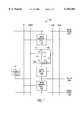
- FIG. 1is a block diagram of one embodiment of a ternary CAM cell
- FIG. 2is a circuit diagram of one embodiment of the ternary CAM cell of FIG. 1.
- circuits and devicesare shown in block diagram form to avoid obscuring the present invention unnecessarily.
- interconnection between circuit elements or blocksmay be shown as buses or as single signal lines.
- Each of the busesmay alternatively be single signal lines, and each of the single signal lines may alternatively be buses.
- the prefix symbol "/" or the suffix "B" attached to signal namesindicates that the signal is an active low signal.
- Each of the active low signalsmay be changed to active high signals as generally known in the art.
- the ternary CAM cellincludes a main memory cell, a compare circuit, a mask memory cell and a mask circuit.
- the main memory cellis coupled to a first pair of bit lines that carries data to and from the main memory cell.
- the compare circuitreceives comparand data on a pair of compare signal lines, and compares the comparand data with the data stored in the main memory cell.
- the compare circuitincludes a pair of transistors and a match transistor. The pair of transistors receives the comparand data on the compare signal lines and also receives the data stored in the main memory cell.
- the match transistordetermines the state of a match line.
- the mask memory cellstores mask data that may mask the comparison result such that it does not affect the logical state of the match line.
- the ternary CAM cell of the present inventiondecouples the read/write accesses to the main memory cell from compare operations.
- Comparand datais provided on compare signal lines while read and write data is carried on traditional data bit lines.
- By separating the compare signal lines from the data bit linesa fewer number of transistors is coupled to each of the compare signal lines and the data bit lines than if a single set of signal lines carried both comparand data and read/write data. This increases the speed of the compare operation and the speed of read/write operations. Since the compare signal lines and data bit lines have reduced capacitance, this can also decrease the power drawn by the ternary CAM cell over other ternary CAM cells that share the same set of signal lines.
- FIG. 1shows ternary CAM cell 100 that is one embodiment of a ternary CAM cell according to the present invention.
- Ternary CAM cell 100includes main memory cell 102, compare circuit 104, mask circuit 106, and mask memory cell 108.
- Main memory cell 102stores data to be compared with comparand data provided on compare signal lines CMP and CMPB.
- Main memory cellmay be any type of memory storage element including a volatile or nonvolatile memory storage element.
- Datais written to and read from main memory cell 102 through data bit lines BL and BLB when the main word line is asserted to a predetermined logic state. For alternative embodiments, data may be read from or written to main memory cell 102 through only one of BL or BLB.
- Mask memory cell 108stores local mask data for ternary CAM cell 100.
- the local mask dataindicates whether the comparison of the comparand data with the data stored in main memory cell 102 will be reflected on the match line.
- Mask memory cell 108may be any type of memory storage element including a volatile or nonvolatile memory storage element.
- the local mask datamay be written to or read from mask memory cell 108 through data bit lines BL and BLB when the mask word line is asserted to a predetermined logic state. For another embodiment, one word line may be shared by both main memory cell 102 and mask memory cell 108.
- the local mask datamay also be read from or written to mask memory cell 108 through only one of BL or BLB.
- another set of data bit linesmay be provided to separately provide local mask data to and from mask memory cell 108 independent of the data bit lines BL and BLB. This may further increase the speed of reading and writing data to main memory cell 102 and local mask data to mask memory cell 108 as the number of transistors coupled to each signal line, and thus the capacitance on each signal line, will be reduced. This may further reduce the power drawn by ternary CAM cell 100 during read and write operations.
- Compare circuit 104compares the data stored in main memory cell 102 with comparand data provided on compare signal lines CMP and CMPB.
- Compare circuit 104includes transistors 110, 112, and 114 that perform the comparison function. Each of transistors 110, 112, and 114 are shown as NMOS transistors, however, they may also be implemented as PMOS transistors.
- Transistor 110has its source coupled to CMPB, its drain coupled to node 111, and its gate coupled to main memory cell 102 to receive data (D) stored therein.
- Transistor 112has its source coupled to CMP, its drain coupled to node 111, and its gate coupled to main memory cell 102 to receive complementary data (DB) stored therein.
- Transistor 114is a match transistor that will pull the match line to a low logic state when the comparand data matches the data stored in main memory cell 102 so long as mask circuit 106 does not mask the comparison result. Note that transistors 110 and 112 are not connected directly to bit lines BL and BLB thereby reducing the capacitance on these signal lines over implementations in which the comparand data and the read/write data are provided over BL and BLB.
- the local mask data stored in mask memory cell 108is provided to mask circuit 106.
- Mask circuit 106determines whether the compare result generated by compare circuit 104 will affect the logical state of the match line. When the local mask data indicates that the comparison should be masked, mask circuit 106 decouples or isolates compare circuit 104 from the match line such that the comparison results do not affect the match line. When the local mask data indicates that the comparison should not be masked, mask circuit 106 allows the comparison result generated by compare circuit 104 to affect the logic state of the match line.
- the match lineis initially pre-charged to a high logic state by pre-charge circuit 116. If there is unmasked match or a masked mismatch, the match line will remain pre-charged to a high logic state. If there is an unmasked mismatch, however, compare circuit 104 will discharge the match line to a low logic state.
- the match line of each row of ternary CAM cellsmay then be provided to a priority encoder that may determine the address, location or index of the highest priority matching entry in the CAM array.
- FIG. 2shows ternary CAM cell 200 that is one embodiment of ternary CAM cell 100.
- Ternary CAM cell 200includes main memory cell 202, mask circuit 206, mask memory cell 208 and pre-charge circuit 216 that are exemplary embodiments of main memory cell 102, mask circuit 106, mask memory cell 108, and pre-charge circuit 116, respectively. Many other embodiments may be used for each of these circuits.
- Main memory cell 202is a bi-stable memory circuit that includes two inverters 222 and 224 cross-coupled (output of one inverter coupled to the input of the other) between nodes 219 and 221.
- Inverters 222 and 224may be any types of inverters including CMOS inverters, NMOS inverters, or the like.
- Node 219stores D and node 221 stores DB.
- Main memory cell 202also includes pass transistors 218 and 220 that communicate data on BL and BLB with nodes 219 and 221, respectively, in response to the logical state of the main word line.
- Node 219is coupled to the gate of transistor 110, and node 221 is coupled to the gate of transistor 112.
- Mask memory cell 208is also a bi-stable memory circuit that includes two inverters 226 and 228 cross-coupled between nodes 229 and 231.
- Inverters 226 and 228may be any types of inverters including CMOS inverters, NMOS inverters, or the like.
- Node 229stores local mask data MD and node 221 stores the logical complement MDB.
- Mask memory cell 208also includes pass transistors 230 and 232 that communicate local mask data on BL and BLB with nodes 229 and 231, respectively, in response to the logical state of the mask word line.
- Node 231is coupled to the gate of mask transistor 206.
- Mask transistor 206is one embodiment of mask circuit 106.
- Mask transistor 206has its drain coupled to the drain of match transistor 114, its gate coupled to node 229 of mask memory cell 208, and its source coupled to the match line.
- the local mask data MDBis a low logic state (MD in a high logic state) indicating a mask condition
- mask transistor 206is off such that the compare results generated by compare circuit 104 do not affect the logical state of the match line.
- the local mask data MDBis in a high logic state (MD in a low logic state) indicating a non-mask condition
- mask transistor 206is on such that the compare results generated by compare circuit 104 affect the logical state of the match line.
- transistor 206is coupled in series with transistor 114 between the match line and ground. Any series arrangement may be used.
- ternary CAM cell 200The operation of ternary CAM cell 200 is as follows. Assume that main memory cell 208 stores a logic one state. Thus, node 219 stores a high logic state causing transistor 110 to be on, and node 221 stores a low logic state causing transistor 112 to be off. If the comparand data is also a logic one, then CMP will have a high logic state and CMPB will have a low logic state. Since transistor 110 is on, the low logic state on CMPB will be communicated to node 111 and turn transistor 114 off. When transistor 114 is off, the match line will remain pre-charged to a high logic state by PMOS transistor 216 to indicate a match.
- CMPBwill have a high logic state.
- Transistor 110will transfer this high logic state to node 111 and cause transistor 114 to turn on. If the comparison is unmasked by the local mask data (MDB a high logic state), transistor 206 is also turned on and the match line is discharged to a low logic state indicating a mismatch condition. If, however, the comparison is masked by the local mask data (MDB a low logic state), transistor 206 is turned off and the match line remains pre-charged by transistor 216.
- main memory cell 208stores a logic zero state.
- node 219stores a low logic state causing transistor 110 to be off
- node 221stores a high logic state causing transistor 112 to be on.
- CMPwill have a low logic state
- CMPBwill have a high logic state. Since transistor 112 is on, the low logic state on CMP will be communicated to node 111 and turn transistor 114 off.
- transistor 114is off, the match line will remain pre-charged to a high logic state by PMOS transistor 216 to indicate a match. If, however, the comparand data is a logic one, then CMP will have a high logic state.
- Transistor 112will transfer this high logic state to node 111 and cause transistor 114 to turn on. If the comparison is unmasked by the local mask data (MDB a high logic state), transistor 206 is also turned on and the match line is discharged to a low logic state indicating a mismatch condition. If, however, the comparison is masked by the local mask data (MDB a low logic state), transistor 206 is turned off and the match line remains pre-charged by transistor 216.
Landscapes
- Static Random-Access Memory (AREA)
Abstract
Description
TABLE 1 ______________________________________ D CMP MDB Match Line ______________________________________ 0 0 0 1 0 0 1 1 0 1 0 1 0 1 1 0 1 0 0 1 1 0 1 0 1 1 0 1 1 1 1 1 ______________________________________
Claims (19)
Priority Applications (1)
| Application Number | Priority Date | Filing Date | Title |
|---|---|---|---|
| US09/439,317US6154384A (en) | 1999-11-12 | 1999-11-12 | Ternary content addressable memory cell |
Applications Claiming Priority (1)
| Application Number | Priority Date | Filing Date | Title |
|---|---|---|---|
| US09/439,317US6154384A (en) | 1999-11-12 | 1999-11-12 | Ternary content addressable memory cell |
Publications (1)
| Publication Number | Publication Date |
|---|---|
| US6154384Atrue US6154384A (en) | 2000-11-28 |
Family
ID=23744206
Family Applications (1)
| Application Number | Title | Priority Date | Filing Date |
|---|---|---|---|
| US09/439,317Expired - LifetimeUS6154384A (en) | 1999-11-12 | 1999-11-12 | Ternary content addressable memory cell |
Country Status (1)
| Country | Link |
|---|---|
| US (1) | US6154384A (en) |
Cited By (101)
| Publication number | Priority date | Publication date | Assignee | Title |
|---|---|---|---|---|
| US6373739B1 (en)* | 2000-12-06 | 2002-04-16 | Integrated Device Technology, Inc. | Quad CAM cell with minimum cell size |
| US6418042B1 (en)* | 1997-10-30 | 2002-07-09 | Netlogic Microsystems, Inc. | Ternary content addressable memory with compare operand selected according to mask value |
| US20020089937A1 (en)* | 2000-11-16 | 2002-07-11 | Srinivasan Venkatachary | Packet matching method and system |
| US6421265B1 (en)* | 2001-03-22 | 2002-07-16 | Integrated Devices Technology, Inc. | DRAM-based CAM cell using 3T or 4T DRAM cells |
| US6496399B1 (en) | 2001-08-28 | 2002-12-17 | Integrated Device Technology, Inc. | Compact ternary content addressable memory cell |
| US6522562B2 (en) | 2001-04-03 | 2003-02-18 | Mosaid Technologies Incorporated | Content addressable memory cell having improved layout |
| US6526474B1 (en) | 1999-10-25 | 2003-02-25 | Cisco Technology, Inc. | Content addressable memory (CAM) with accesses to multiple CAM arrays used to generate result for various matching sizes |
| US6532516B1 (en) | 2001-09-27 | 2003-03-11 | Coriolis Networks, Inc. | Technique for updating a content addressable memory |
| US20030056001A1 (en)* | 2001-07-20 | 2003-03-20 | Ashutosh Mate | Selective routing of data flows using a TCAM |
| WO2003027854A1 (en)* | 2001-09-27 | 2003-04-03 | Coriolis Networks, Inc. | Technique for updating a content addressable memory |
| US6597595B1 (en) | 2001-08-03 | 2003-07-22 | Netlogic Microsystems, Inc. | Content addressable memory with error detection signaling |
| US6597594B2 (en)* | 2000-03-17 | 2003-07-22 | Silicon Aquarius, Inc. | Content addressable memory cells and systems and devices using the same |
| US6606681B1 (en) | 2001-02-23 | 2003-08-12 | Cisco Systems, Inc. | Optimized content addressable memory (CAM) |
| US6615210B1 (en)* | 2000-02-04 | 2003-09-02 | Broad Web Corporation | Bit stream ternary match scheme |
| US6615311B2 (en)* | 2001-06-07 | 2003-09-02 | Riverstone Networks, Inc. | Method and system for updating a content addressable memory (CAM) that prioritizes CAM entries according to prefix length |
| US20030169612A1 (en)* | 2002-03-08 | 2003-09-11 | Hu Shane Ching-Feng | Static content addressable memory cell |
| US6646900B2 (en) | 2001-10-31 | 2003-11-11 | Kawasaki Microelectronics, Inc. | Ternary content addressable memory with data and mask data settable therewithin by one write cycle |
| US6658002B1 (en) | 1998-06-30 | 2003-12-02 | Cisco Technology, Inc. | Logical operation unit for packet processing |
| US6661687B1 (en)* | 2002-06-06 | 2003-12-09 | Integrated Device Technology, Inc. | Cam circuit with separate memory and logic operating voltages |
| WO2003079369A3 (en)* | 2002-03-18 | 2003-12-18 | Infineon Technologies Ag | Content addressable memory cell |
| US20040001347A1 (en)* | 2002-06-28 | 2004-01-01 | Chul-Sung Park | Ternary content addressable memory device |
| US20040030803A1 (en)* | 2002-08-10 | 2004-02-12 | Eatherton William N. | Performing lookup operations using associative memories optionally including modifying a search key in generating a lookup word and possibly forcing a no-hit indication in response to matching a particular entry |
| US20040030802A1 (en)* | 2002-08-10 | 2004-02-12 | Eatherton William N. | Performing lookup operations using associative memories optionally including selectively determining which associative memory blocks to use in identifying a result and possibly propagating error indications |
| US6715029B1 (en) | 2002-01-07 | 2004-03-30 | Cisco Technology, Inc. | Method and apparatus for possibly decreasing the number of associative memory entries by supplementing an associative memory result with discriminator bits from an original set of information |
| US6721202B1 (en) | 2001-12-21 | 2004-04-13 | Cypress Semiconductor Corp. | Bit encoded ternary content addressable memory cell |
| US6745280B2 (en) | 2002-03-28 | 2004-06-01 | Integrated Device Technology, Inc. | Content addressable memories having entries stored therein with independently searchable weight fields and methods of operating same |
| KR20040048651A (en)* | 2002-12-04 | 2004-06-10 | 삼성전자주식회사 | Ternary content addressable memory cell |
| US6760881B2 (en) | 2001-10-16 | 2004-07-06 | International Business Machines Corporation | Method for combining refresh operation with parity validation in a DRAM-based content addressable memory (CAM) |
| US6760241B1 (en) | 2002-10-18 | 2004-07-06 | Netlogic Microsystems, Inc. | Dynamic random access memory (DRAM) based content addressable memory (CAM) cell |
| US20040170172A1 (en)* | 2002-08-10 | 2004-09-02 | Cisco Technology, Inc., A California Corporation | Associative memory entries with force no-hit and priority indications of particular use in implementing policy maps in communication devices |
| US20040170171A1 (en)* | 2002-08-10 | 2004-09-02 | Cisco Technology, Inc., A California Corporation | Generating and merging lookup results to apply multiple features |
| US20040172346A1 (en)* | 2002-08-10 | 2004-09-02 | Cisco Technology, Inc., A California Corporation | Generating accounting data based on access control list entries |
| DE10310858A1 (en)* | 2003-03-11 | 2004-09-23 | Bergische Universität Wuppertal | Character string compression method for compressing computer data, whereby data on a data bus to a memory component is compared with data stored in the memory to find the longest possible match |
| US20040193619A1 (en)* | 2003-03-28 | 2004-09-30 | Srinivasan Venkatachary | System and method for efficiently searching a forwarding database that is split into a bounded number of sub-databases having a bounded size |
| US6801981B1 (en) | 2000-06-14 | 2004-10-05 | Netlogic Microsystems, Inc. | Intra-row configurability of content addressable memory |
| US6813680B1 (en) | 2000-06-14 | 2004-11-02 | Netlogic Microsystems, Inc. | Method and apparatus for loading comparand data into a content addressable memory system |
| US20040249803A1 (en)* | 2003-06-05 | 2004-12-09 | Srinivasan Vankatachary | Architecture for network search engines with fixed latency, high capacity, and high throughput |
| US6842360B1 (en) | 2003-05-30 | 2005-01-11 | Netlogic Microsystems, Inc. | High-density content addressable memory cell |
| US20050010612A1 (en)* | 2003-07-09 | 2005-01-13 | Cisco Technology, Inc. | Storing and searching a hierarchy of items of particular use with IP security policies and security associations |
| US20050021752A1 (en)* | 2002-08-10 | 2005-01-27 | Cisco Technology, Inc., A California Corporation | Reverse path forwarding protection of packets using automated population of access control lists based on a forwarding information base |
| US6856527B1 (en) | 2003-05-30 | 2005-02-15 | Netlogic Microsystems, Inc. | Multi-compare content addressable memory cell |
| US6862281B1 (en) | 2001-05-10 | 2005-03-01 | Cisco Technology, Inc. | L4 lookup implementation using efficient CAM organization |
| US6871262B1 (en) | 2002-02-14 | 2005-03-22 | Cisco Technology, Inc. | Method and apparatus for matching a string with multiple lookups using a single associative memory |
| US6870749B1 (en) | 2003-07-15 | 2005-03-22 | Integrated Device Technology, Inc. | Content addressable memory (CAM) devices with dual-function check bit cells that support column redundancy and check bit cells with reduced susceptibility to soft errors |
| US6879504B1 (en) | 2001-02-08 | 2005-04-12 | Integrated Device Technology, Inc. | Content addressable memory (CAM) devices having error detection and correction control circuits therein and methods of operating same |
| US6888730B2 (en) | 2001-04-03 | 2005-05-03 | Mosaid Technologies Incorporated | Content addressable memory cell |
| US6910097B1 (en)* | 2001-04-09 | 2005-06-21 | Netlogic Microsystems, Inc. | Classless interdomain routing using binary content addressable memory |
| US6914795B1 (en) | 2001-08-03 | 2005-07-05 | Netlogic Microsystems, Inc. | Content addressable memory with selective error logging |
| US20050146947A1 (en)* | 2004-01-05 | 2005-07-07 | Hitachi, Ltd. | Semiconductor device |
| US20050152167A1 (en)* | 2004-01-13 | 2005-07-14 | Hitachi, Ltd. | Semiconductor memory device |
| US6934795B2 (en) | 1999-09-23 | 2005-08-23 | Netlogic Microsystems, Inc. | Content addressable memory with programmable word width and programmable priority |
| US6944709B2 (en) | 1999-09-23 | 2005-09-13 | Netlogic Microsystems, Inc. | Content addressable memory with block-programmable mask write mode, word width and priority |
| US6961808B1 (en) | 2002-01-08 | 2005-11-01 | Cisco Technology, Inc. | Method and apparatus for implementing and using multiple virtual portions of physical associative memories |
| US20050276086A1 (en)* | 2004-06-01 | 2005-12-15 | Douglas Perry | Ternary CAM cell for reduced matchline capacitance |
| US6978343B1 (en) | 2002-08-05 | 2005-12-20 | Netlogic Microsystems, Inc. | Error-correcting content addressable memory |
| US20050289295A1 (en)* | 2004-06-29 | 2005-12-29 | Cisco Technology, Inc. | Error Protection For Lookup Operations in Content-Addressable Memory Entries |
| US6987684B1 (en) | 2003-07-15 | 2006-01-17 | Integrated Device Technology, Inc. | Content addressable memory (CAM) devices having multi-block error detection logic and entry selective error correction logic therein |
| US7002965B1 (en) | 2001-05-21 | 2006-02-21 | Cisco Technology, Inc. | Method and apparatus for using ternary and binary content-addressable memory stages to classify packets |
| US7002823B1 (en) | 2001-08-03 | 2006-02-21 | Netlogic Microsystems, Inc. | Content addressable memory with simultaneous write and compare function |
| US7028136B1 (en) | 2002-08-10 | 2006-04-11 | Cisco Technology, Inc. | Managing idle time and performing lookup operations to adapt to refresh requirements or operational rates of the particular associative memory or other devices used to implement the system |
| US7043673B1 (en) | 2001-08-03 | 2006-05-09 | Netlogic Microsystems, Inc. | Content addressable memory with priority-biased error detection sequencing |
| US20060106977A1 (en)* | 2002-08-10 | 2006-05-18 | Cisco Technology, Inc. A California Corporation | Performing lookup operations on associative memory entries |
| US7050317B1 (en)* | 2002-03-15 | 2006-05-23 | Integrated Device Technology, Inc. | Content addressable memory (CAM) devices that support power saving longest prefix match operations and methods of operating same |
| US7062571B1 (en)* | 2000-06-30 | 2006-06-13 | Cisco Technology, Inc. | Efficient IP load-balancing traffic distribution using ternary CAMs |
| US7065083B1 (en) | 2001-10-04 | 2006-06-20 | Cisco Technology, Inc. | Method and apparatus for dynamically generating lookup words for content-addressable memories |
| US20060168494A1 (en)* | 2005-01-22 | 2006-07-27 | Cisco Technology, Inc., A California Corporation | Error protecting groups of data words |
| US20060262582A1 (en)* | 2005-05-23 | 2006-11-23 | Stmicroelectronics, Inc. | Physical priority encoder |
| US7174419B1 (en) | 2003-05-30 | 2007-02-06 | Netlogic Microsystems, Inc | Content addressable memory device with source-selecting data translator |
| US7193876B1 (en) | 2003-07-15 | 2007-03-20 | Kee Park | Content addressable memory (CAM) arrays having memory cells therein with different susceptibilities to soft errors |
| US20070064461A1 (en)* | 2003-11-15 | 2007-03-22 | Varadarajan Srinivasan | Low power content addressable memory |
| US7237156B1 (en) | 2001-08-03 | 2007-06-26 | Netlogic Microsystems, Inc. | Content addressable memory with error detection |
| EP1369877A3 (en)* | 2002-06-05 | 2007-08-08 | STMicroelectronics, Inc. | CAM cell |
| US7257763B1 (en)* | 2001-08-03 | 2007-08-14 | Netlogic Microsystems, Inc. | Content addressable memory with error signaling |
| US7260673B1 (en) | 2001-07-20 | 2007-08-21 | Cisco Technology, Inc. | Method and apparatus for verifying the integrity of a content-addressable memory result |
| US7283380B1 (en) | 2001-08-03 | 2007-10-16 | Netlogic Microsystems, Inc. | Content addressable memory with selective error logging |
| US7305519B1 (en) | 2004-03-29 | 2007-12-04 | Cisco Technology, Inc. | Error protection for associative memory entries and lookup operations performed thereon |
| US7304873B1 (en) | 2005-01-25 | 2007-12-04 | Netlogic Microsystems, Inc. | Method for on-the-fly error correction in a content addressable memory (CAM) and device therefor |
| US7304875B1 (en) | 2003-12-17 | 2007-12-04 | Integrated Device Technology. Inc. | Content addressable memory (CAM) devices that support background BIST and BISR operations and methods of operating same |
| US7313666B1 (en) | 2002-08-10 | 2007-12-25 | Cisco Technology, Inc. | Methods and apparatus for longest common prefix based caching |
| US7571156B1 (en) | 2003-03-28 | 2009-08-04 | Netlogic Microsystems, Inc. | Network device, storage medium and methods for incrementally updating a forwarding database |
| US20090262595A1 (en)* | 2008-04-21 | 2009-10-22 | Infineon Technologies Ag | Method and apparatus for operating maskable memory cells |
| US20090323389A1 (en)* | 2008-04-21 | 2009-12-31 | Infineon Technologies Ag | Masked memory cells |
| US20090323439A1 (en)* | 2008-04-21 | 2009-12-31 | Infineon Technologies Ag | Memory for storing a binary state |
| US7694068B1 (en) | 2005-12-08 | 2010-04-06 | Netlogic Microsystems, Inc. | Re-entrant processing in a content addressable memory |
| USRE41351E1 (en) | 2000-05-18 | 2010-05-25 | Netlogic Microsystems, Inc. | CAM arrays having CAM cells therein with match line and low match line connections and methods of operating same |
| US20100205364A1 (en)* | 2009-02-06 | 2010-08-12 | Hillel Gazit | Ternary content-addressable memory |
| US7904642B1 (en) | 2007-02-08 | 2011-03-08 | Netlogic Microsystems, Inc. | Method for combining and storing access control lists |
| US7941605B1 (en) | 2002-11-01 | 2011-05-10 | Cisco Technology, Inc | Methods and apparatus for generating a result based on a lookup result from a lookup operation using an associative memory and processing based on a discriminator portion of a lookup word |
| US8023299B1 (en) | 2009-04-09 | 2011-09-20 | Netlogic Microsystems, Inc. | Content addressable memory device having spin torque transfer memory cells |
| US8073005B1 (en) | 2001-12-27 | 2011-12-06 | Cypress Semiconductor Corporation | Method and apparatus for configuring signal lines according to idle codes |
| US8438330B2 (en) | 2010-05-17 | 2013-05-07 | Netlogic Microsystems, Inc. | Updating cam arrays using prefix length distribution prediction |
| US8462532B1 (en) | 2010-08-31 | 2013-06-11 | Netlogic Microsystems, Inc. | Fast quaternary content addressable memory cell |
| US8553441B1 (en)* | 2010-08-31 | 2013-10-08 | Netlogic Microsystems, Inc. | Ternary content addressable memory cell having two transistor pull-down stack |
| US8582338B1 (en) | 2010-08-31 | 2013-11-12 | Netlogic Microsystems, Inc. | Ternary content addressable memory cell having single transistor pull-down stack |
| US8625320B1 (en) | 2010-08-31 | 2014-01-07 | Netlogic Microsystems, Inc. | Quaternary content addressable memory cell having one transistor pull-down stack |
| US8638582B1 (en) | 2011-08-23 | 2014-01-28 | Netlogic Microsystems, Inc. | Content addressable memory with base-three numeral system |
| US8773880B2 (en) | 2011-06-23 | 2014-07-08 | Netlogic Microsystems, Inc. | Content addressable memory array having virtual ground nodes |
| US8837188B1 (en) | 2011-06-23 | 2014-09-16 | Netlogic Microsystems, Inc. | Content addressable memory row having virtual ground and charge sharing |
| US8990631B1 (en) | 2011-03-03 | 2015-03-24 | Netlogic Microsystems, Inc. | Packet format for error reporting in a content addressable memory |
| US9502112B2 (en) | 2015-02-25 | 2016-11-22 | Renesas Electronics Corporation | Semiconductor memory device |
| US20180040374A1 (en)* | 2016-08-04 | 2018-02-08 | Hewlett Packard Enterprise Development Lp | Ternary content addressable memories having a bit cell with memristors and serially connected match-line transistors |
Citations (13)
| Publication number | Priority date | Publication date | Assignee | Title |
|---|---|---|---|---|
| US5226005A (en)* | 1990-11-19 | 1993-07-06 | Unisys Corporation | Dual ported content addressable memory cell and array |
| US5319590A (en)* | 1992-12-04 | 1994-06-07 | Hal Computer Systems, Inc. | Apparatus for storing "Don't Care" in a content addressable memory cell |
| US5396449A (en)* | 1993-12-21 | 1995-03-07 | International Business Machines Corporation | Fast content addressable memory with reduced power consumption |
| US5446685A (en)* | 1993-02-23 | 1995-08-29 | Intergraph Corporation | Pulsed ground circuit for CAM and PAL memories |
| US5517441A (en)* | 1994-12-14 | 1996-05-14 | International Business Machines Corporation | Content addressable memory circuitry and method of operation |
| US5642114A (en)* | 1993-04-19 | 1997-06-24 | Oki Electric Industry Co., Ltd. | Variable length code decoder using a content addressable memory with match inhibiting gate |
| US5646878A (en)* | 1995-06-02 | 1997-07-08 | Motorola, Inc. | Content addressable memory system |
| US5699288A (en)* | 1996-07-18 | 1997-12-16 | International Business Machines Corporation | Compare circuit for content-addressable memories |
| US5870324A (en)* | 1995-04-18 | 1999-02-09 | International Business Machines Corporation | Contents-addressable memory |
| US5940852A (en)* | 1997-05-01 | 1999-08-17 | Altera Corporation | Memory cells configurable as CAM or RAM in programmable logic devices |
| US5949696A (en)* | 1997-06-30 | 1999-09-07 | Cypress Semiconductor Corporation | Differential dynamic content addressable memory and high speed network address filtering |
| US5993363A (en)* | 1998-10-21 | 1999-11-30 | Chen; Chih-Liang | Exercise machine |
| US6044005A (en)* | 1999-02-03 | 2000-03-28 | Sibercore Technologies Incorporated | Content addressable memory storage device |
- 1999
- 1999-11-12USUS09/439,317patent/US6154384A/ennot_activeExpired - Lifetime
Patent Citations (14)
| Publication number | Priority date | Publication date | Assignee | Title |
|---|---|---|---|---|
| US5226005A (en)* | 1990-11-19 | 1993-07-06 | Unisys Corporation | Dual ported content addressable memory cell and array |
| US5319590A (en)* | 1992-12-04 | 1994-06-07 | Hal Computer Systems, Inc. | Apparatus for storing "Don't Care" in a content addressable memory cell |
| US5598115A (en)* | 1993-02-23 | 1997-01-28 | Intergraph Corporation | Comparator cell for use in a content addressable memory |
| US5446685A (en)* | 1993-02-23 | 1995-08-29 | Intergraph Corporation | Pulsed ground circuit for CAM and PAL memories |
| US5642114A (en)* | 1993-04-19 | 1997-06-24 | Oki Electric Industry Co., Ltd. | Variable length code decoder using a content addressable memory with match inhibiting gate |
| US5396449A (en)* | 1993-12-21 | 1995-03-07 | International Business Machines Corporation | Fast content addressable memory with reduced power consumption |
| US5517441A (en)* | 1994-12-14 | 1996-05-14 | International Business Machines Corporation | Content addressable memory circuitry and method of operation |
| US5870324A (en)* | 1995-04-18 | 1999-02-09 | International Business Machines Corporation | Contents-addressable memory |
| US5646878A (en)* | 1995-06-02 | 1997-07-08 | Motorola, Inc. | Content addressable memory system |
| US5699288A (en)* | 1996-07-18 | 1997-12-16 | International Business Machines Corporation | Compare circuit for content-addressable memories |
| US5940852A (en)* | 1997-05-01 | 1999-08-17 | Altera Corporation | Memory cells configurable as CAM or RAM in programmable logic devices |
| US5949696A (en)* | 1997-06-30 | 1999-09-07 | Cypress Semiconductor Corporation | Differential dynamic content addressable memory and high speed network address filtering |
| US5993363A (en)* | 1998-10-21 | 1999-11-30 | Chen; Chih-Liang | Exercise machine |
| US6044005A (en)* | 1999-02-03 | 2000-03-28 | Sibercore Technologies Incorporated | Content addressable memory storage device |
Non-Patent Citations (5)
| Title |
|---|
| Chae, Soo Ik, et al., Content Addressable Memory for VLSI Pattern Inspection , IEEE Journal Of Solid State Circuits, vol. 23, No. 1, Feb. 1988, pp. 74 78.* |
| Chae, Soo-Ik, et al., "Content-Addressable Memory for VLSI Pattern Inspection", IEEE Journal Of Solid-State Circuits, vol. 23, No. 1, Feb. 1988, pp. 74-78. |
| Japanese Patent Abstract, Publication No. 04021997 A, published Jan. 24, 1992, 1 page.* |
| Japanese Patent Abstract, Publication No. 05182472 A, published Jul. 23, 1993, 1 page.* |
| MOSAID, The Next Generation of Content Addressable Memories, MOSAID Technologies Incorporated, Sep. 1999, 8 pages.* |
Cited By (179)
| Publication number | Priority date | Publication date | Assignee | Title |
|---|---|---|---|---|
| US6418042B1 (en)* | 1997-10-30 | 2002-07-09 | Netlogic Microsystems, Inc. | Ternary content addressable memory with compare operand selected according to mask value |
| US6658002B1 (en) | 1998-06-30 | 2003-12-02 | Cisco Technology, Inc. | Logical operation unit for packet processing |
| US7246198B2 (en) | 1999-09-23 | 2007-07-17 | Netlogic Microsystems, Inc. | Content addressable memory with programmable word width and programmable priority |
| US6934795B2 (en) | 1999-09-23 | 2005-08-23 | Netlogic Microsystems, Inc. | Content addressable memory with programmable word width and programmable priority |
| US6944709B2 (en) | 1999-09-23 | 2005-09-13 | Netlogic Microsystems, Inc. | Content addressable memory with block-programmable mask write mode, word width and priority |
| US6526474B1 (en) | 1999-10-25 | 2003-02-25 | Cisco Technology, Inc. | Content addressable memory (CAM) with accesses to multiple CAM arrays used to generate result for various matching sizes |
| US6615210B1 (en)* | 2000-02-04 | 2003-09-02 | Broad Web Corporation | Bit stream ternary match scheme |
| US6597594B2 (en)* | 2000-03-17 | 2003-07-22 | Silicon Aquarius, Inc. | Content addressable memory cells and systems and devices using the same |
| USRE41351E1 (en) | 2000-05-18 | 2010-05-25 | Netlogic Microsystems, Inc. | CAM arrays having CAM cells therein with match line and low match line connections and methods of operating same |
| US6801981B1 (en) | 2000-06-14 | 2004-10-05 | Netlogic Microsystems, Inc. | Intra-row configurability of content addressable memory |
| US6813680B1 (en) | 2000-06-14 | 2004-11-02 | Netlogic Microsystems, Inc. | Method and apparatus for loading comparand data into a content addressable memory system |
| US7062571B1 (en)* | 2000-06-30 | 2006-06-13 | Cisco Technology, Inc. | Efficient IP load-balancing traffic distribution using ternary CAMs |
| US20020089937A1 (en)* | 2000-11-16 | 2002-07-11 | Srinivasan Venkatachary | Packet matching method and system |
| US7978709B1 (en) | 2000-11-16 | 2011-07-12 | Netlogic Microsystems, Inc. | Packet matching method and system |
| US6373739B1 (en)* | 2000-12-06 | 2002-04-16 | Integrated Device Technology, Inc. | Quad CAM cell with minimum cell size |
| US6879504B1 (en) | 2001-02-08 | 2005-04-12 | Integrated Device Technology, Inc. | Content addressable memory (CAM) devices having error detection and correction control circuits therein and methods of operating same |
| US6606681B1 (en) | 2001-02-23 | 2003-08-12 | Cisco Systems, Inc. | Optimized content addressable memory (CAM) |
| US6421265B1 (en)* | 2001-03-22 | 2002-07-16 | Integrated Devices Technology, Inc. | DRAM-based CAM cell using 3T or 4T DRAM cells |
| CN100437828C (en)* | 2001-04-03 | 2008-11-26 | 睦塞德技术公司 | Content-addressed memory unit |
| US20030161173A1 (en)* | 2001-04-03 | 2003-08-28 | Richard Foss | Content addressable memory cell having improved layout |
| US6888730B2 (en) | 2001-04-03 | 2005-05-03 | Mosaid Technologies Incorporated | Content addressable memory cell |
| US6873532B2 (en) | 2001-04-03 | 2005-03-29 | Mosaid Technologies Incorporated | Content addressable memory cell having improved layout |
| US6522562B2 (en) | 2001-04-03 | 2003-02-18 | Mosaid Technologies Incorporated | Content addressable memory cell having improved layout |
| US7054993B1 (en) | 2001-04-09 | 2006-05-30 | Netlogic Microsystems, Inc. | Ternary content addressable memory device |
| US6910097B1 (en)* | 2001-04-09 | 2005-06-21 | Netlogic Microsystems, Inc. | Classless interdomain routing using binary content addressable memory |
| US6862281B1 (en) | 2001-05-10 | 2005-03-01 | Cisco Technology, Inc. | L4 lookup implementation using efficient CAM organization |
| US20060104286A1 (en)* | 2001-05-21 | 2006-05-18 | Cisco Technology, Inc., A California Corporation | Using ternary and binary content addressable memory stages to classify information such as packets |
| US7002965B1 (en) | 2001-05-21 | 2006-02-21 | Cisco Technology, Inc. | Method and apparatus for using ternary and binary content-addressable memory stages to classify packets |
| US7602787B2 (en) | 2001-05-21 | 2009-10-13 | Cisco Technology, Inc. | Using ternary and binary content addressable memory stages to classify information such as packets |
| US6615311B2 (en)* | 2001-06-07 | 2003-09-02 | Riverstone Networks, Inc. | Method and system for updating a content addressable memory (CAM) that prioritizes CAM entries according to prefix length |
| US7028098B2 (en) | 2001-07-20 | 2006-04-11 | Nokia, Inc. | Selective routing of data flows using a TCAM |
| US7260673B1 (en) | 2001-07-20 | 2007-08-21 | Cisco Technology, Inc. | Method and apparatus for verifying the integrity of a content-addressable memory result |
| US20030056001A1 (en)* | 2001-07-20 | 2003-03-20 | Ashutosh Mate | Selective routing of data flows using a TCAM |
| US7257763B1 (en)* | 2001-08-03 | 2007-08-14 | Netlogic Microsystems, Inc. | Content addressable memory with error signaling |
| US7283380B1 (en) | 2001-08-03 | 2007-10-16 | Netlogic Microsystems, Inc. | Content addressable memory with selective error logging |
| US6707693B1 (en) | 2001-08-03 | 2004-03-16 | Netlogic Microsystems, Inc. | Content addressable memory with simultaneous write and compare function |
| US6700810B1 (en) | 2001-08-03 | 2004-03-02 | Netlogic Microsystems, Inc. | Content addressable memory with error detection signaling |
| US7237156B1 (en) | 2001-08-03 | 2007-06-26 | Netlogic Microsystems, Inc. | Content addressable memory with error detection |
| US6690595B1 (en) | 2001-08-03 | 2004-02-10 | Netlogic Microsystems, Inc. | Content addressable memory with selective error logging |
| US7002823B1 (en) | 2001-08-03 | 2006-02-21 | Netlogic Microsystems, Inc. | Content addressable memory with simultaneous write and compare function |
| US6914795B1 (en) | 2001-08-03 | 2005-07-05 | Netlogic Microsystems, Inc. | Content addressable memory with selective error logging |
| US7043673B1 (en) | 2001-08-03 | 2006-05-09 | Netlogic Microsystems, Inc. | Content addressable memory with priority-biased error detection sequencing |
| US6597595B1 (en) | 2001-08-03 | 2003-07-22 | Netlogic Microsystems, Inc. | Content addressable memory with error detection signaling |
| US6728124B1 (en) | 2001-08-03 | 2004-04-27 | Netlogic Microsystems, Inc. | Content addressable memory with error detection signaling |
| US6496399B1 (en) | 2001-08-28 | 2002-12-17 | Integrated Device Technology, Inc. | Compact ternary content addressable memory cell |
| US6532516B1 (en) | 2001-09-27 | 2003-03-11 | Coriolis Networks, Inc. | Technique for updating a content addressable memory |
| WO2003027854A1 (en)* | 2001-09-27 | 2003-04-03 | Coriolis Networks, Inc. | Technique for updating a content addressable memory |
| US6574701B2 (en) | 2001-09-27 | 2003-06-03 | Coriolis Networks, Inc. | Technique for updating a content addressable memory |
| WO2003027855A1 (en)* | 2001-09-27 | 2003-04-03 | Coriolis Networks, Inc. | Technique for updating a content addressable memory |
| US7065083B1 (en) | 2001-10-04 | 2006-06-20 | Cisco Technology, Inc. | Method and apparatus for dynamically generating lookup words for content-addressable memories |
| US6760881B2 (en) | 2001-10-16 | 2004-07-06 | International Business Machines Corporation | Method for combining refresh operation with parity validation in a DRAM-based content addressable memory (CAM) |
| US6646900B2 (en) | 2001-10-31 | 2003-11-11 | Kawasaki Microelectronics, Inc. | Ternary content addressable memory with data and mask data settable therewithin by one write cycle |
| US6721202B1 (en) | 2001-12-21 | 2004-04-13 | Cypress Semiconductor Corp. | Bit encoded ternary content addressable memory cell |
| US8073005B1 (en) | 2001-12-27 | 2011-12-06 | Cypress Semiconductor Corporation | Method and apparatus for configuring signal lines according to idle codes |
| US6715029B1 (en) | 2002-01-07 | 2004-03-30 | Cisco Technology, Inc. | Method and apparatus for possibly decreasing the number of associative memory entries by supplementing an associative memory result with discriminator bits from an original set of information |
| US6961808B1 (en) | 2002-01-08 | 2005-11-01 | Cisco Technology, Inc. | Method and apparatus for implementing and using multiple virtual portions of physical associative memories |
| US6871262B1 (en) | 2002-02-14 | 2005-03-22 | Cisco Technology, Inc. | Method and apparatus for matching a string with multiple lookups using a single associative memory |
| US7099172B2 (en) | 2002-03-08 | 2006-08-29 | Micron Technology, Inc. | Static content addressable memory cell |
| US6952359B2 (en) | 2002-03-08 | 2005-10-04 | Micron Technology, Inc. | Static content addressable memory cell |
| US20060114705A1 (en)* | 2002-03-08 | 2006-06-01 | Hu Shane C | Static content addressable memory cell |
| US20030169612A1 (en)* | 2002-03-08 | 2003-09-11 | Hu Shane Ching-Feng | Static content addressable memory cell |
| US7269040B2 (en) | 2002-03-08 | 2007-09-11 | Micron Technology, Inc. | Static content addressable memory cell |
| US20060181911A1 (en)* | 2002-03-08 | 2006-08-17 | Hu Shane C | Static content addressable memory cell |
| US7307860B2 (en) | 2002-03-08 | 2007-12-11 | Micron Technology, Inc. | Static content addressable memory cell |
| US6751110B2 (en)* | 2002-03-08 | 2004-06-15 | Micron Technology, Inc. | Static content addressable memory cell |
| US20040095794A1 (en)* | 2002-03-08 | 2004-05-20 | Hu Shane Ching-Feng | Static content addressable memory cell |
| US6888732B2 (en) | 2002-03-08 | 2005-05-03 | Micron Technology, Inc. | Static content addressable memory cell |
| US20050190639A1 (en)* | 2002-03-08 | 2005-09-01 | Hu Shane C. | Static content addressable memory cell |
| US20040095793A1 (en)* | 2002-03-08 | 2004-05-20 | Hu Shane Ching-Feng | Static content addressable memory cell |
| US7050317B1 (en)* | 2002-03-15 | 2006-05-23 | Integrated Device Technology, Inc. | Content addressable memory (CAM) devices that support power saving longest prefix match operations and methods of operating same |
| WO2003079369A3 (en)* | 2002-03-18 | 2003-12-18 | Infineon Technologies Ag | Content addressable memory cell |
| DE10211957B4 (en)* | 2002-03-18 | 2007-03-08 | Infineon Technologies Ag | Ternary content addressable memory cell |
| US6977831B2 (en)* | 2002-03-18 | 2005-12-20 | Infineon Technologies Ag | Content addressable memory cell |
| CN100466103C (en)* | 2002-03-18 | 2009-03-04 | 因芬尼昂技术股份公司 | Content-addressable storage unit |
| US20050094477A1 (en)* | 2002-03-18 | 2005-05-05 | Joel Hatsch | Content addressable memory cell |
| US6745280B2 (en) | 2002-03-28 | 2004-06-01 | Integrated Device Technology, Inc. | Content addressable memories having entries stored therein with independently searchable weight fields and methods of operating same |
| EP1369877A3 (en)* | 2002-06-05 | 2007-08-08 | STMicroelectronics, Inc. | CAM cell |
| US20030227789A1 (en)* | 2002-06-06 | 2003-12-11 | Integrated Device Technology, Inc. | Cam circuit with separate memory and logic operating voltages |
| US6661687B1 (en)* | 2002-06-06 | 2003-12-09 | Integrated Device Technology, Inc. | Cam circuit with separate memory and logic operating voltages |
| US6747885B2 (en) | 2002-06-28 | 2004-06-08 | Samsung Electronics Co., Ltd. | Ternary content addressable memory device |
| US20040001347A1 (en)* | 2002-06-28 | 2004-01-01 | Chul-Sung Park | Ternary content addressable memory device |
| EP1376607A3 (en)* | 2002-06-28 | 2005-09-14 | Samsung Electronics Co., Ltd. | Content addressable memory device and method of operating same |
| US6978343B1 (en) | 2002-08-05 | 2005-12-20 | Netlogic Microsystems, Inc. | Error-correcting content addressable memory |
| US20040030803A1 (en)* | 2002-08-10 | 2004-02-12 | Eatherton William N. | Performing lookup operations using associative memories optionally including modifying a search key in generating a lookup word and possibly forcing a no-hit indication in response to matching a particular entry |
| US7082492B2 (en) | 2002-08-10 | 2006-07-25 | Cisco Technology, Inc. | Associative memory entries with force no-hit and priority indications of particular use in implementing policy maps in communication devices |
| US7313666B1 (en) | 2002-08-10 | 2007-12-25 | Cisco Technology, Inc. | Methods and apparatus for longest common prefix based caching |
| US7350020B2 (en) | 2002-08-10 | 2008-03-25 | Cisco Technology, Inc. | Generating and merging lookup results to apply multiple features |
| US20060106977A1 (en)* | 2002-08-10 | 2006-05-18 | Cisco Technology, Inc. A California Corporation | Performing lookup operations on associative memory entries |
| US7349382B2 (en) | 2002-08-10 | 2008-03-25 | Cisco Technology, Inc. | Reverse path forwarding protection of packets using automated population of access control lists based on a forwarding information base |
| US7441074B1 (en) | 2002-08-10 | 2008-10-21 | Cisco Technology, Inc. | Methods and apparatus for distributing entries among lookup units and selectively enabling less than all of the lookup units when performing a lookup operation |
| US7689485B2 (en) | 2002-08-10 | 2010-03-30 | Cisco Technology, Inc. | Generating accounting data based on access control list entries |
| US20050021752A1 (en)* | 2002-08-10 | 2005-01-27 | Cisco Technology, Inc., A California Corporation | Reverse path forwarding protection of packets using automated population of access control lists based on a forwarding information base |
| US7065609B2 (en) | 2002-08-10 | 2006-06-20 | Cisco Technology, Inc. | Performing lookup operations using associative memories optionally including selectively determining which associative memory blocks to use in identifying a result and possibly propagating error indications |
| US7177978B2 (en) | 2002-08-10 | 2007-02-13 | Cisco Technology, Inc. | Generating and merging lookup results to apply multiple features |
| US7028136B1 (en) | 2002-08-10 | 2006-04-11 | Cisco Technology, Inc. | Managing idle time and performing lookup operations to adapt to refresh requirements or operational rates of the particular associative memory or other devices used to implement the system |
| US20040172346A1 (en)* | 2002-08-10 | 2004-09-02 | Cisco Technology, Inc., A California Corporation | Generating accounting data based on access control list entries |
| US20040170171A1 (en)* | 2002-08-10 | 2004-09-02 | Cisco Technology, Inc., A California Corporation | Generating and merging lookup results to apply multiple features |
| US20040170172A1 (en)* | 2002-08-10 | 2004-09-02 | Cisco Technology, Inc., A California Corporation | Associative memory entries with force no-hit and priority indications of particular use in implementing policy maps in communication devices |
| US7103708B2 (en) | 2002-08-10 | 2006-09-05 | Cisco Technology, Inc. | Performing lookup operations using associative memories optionally including modifying a search key in generating a lookup word and possibly forcing a no-hit indication in response to matching a particular entry |
| US7237059B2 (en) | 2002-08-10 | 2007-06-26 | Cisco Technology, Inc | Performing lookup operations on associative memory entries |
| US20040030802A1 (en)* | 2002-08-10 | 2004-02-12 | Eatherton William N. | Performing lookup operations using associative memories optionally including selectively determining which associative memory blocks to use in identifying a result and possibly propagating error indications |
| US20070002862A1 (en)* | 2002-08-10 | 2007-01-04 | Cisco Technology, Inc., A California Corporation | Generating and merging lookup results to apply multiple features |
| US6760241B1 (en) | 2002-10-18 | 2004-07-06 | Netlogic Microsystems, Inc. | Dynamic random access memory (DRAM) based content addressable memory (CAM) cell |
| US7941605B1 (en) | 2002-11-01 | 2011-05-10 | Cisco Technology, Inc | Methods and apparatus for generating a result based on a lookup result from a lookup operation using an associative memory and processing based on a discriminator portion of a lookup word |
| KR20040048651A (en)* | 2002-12-04 | 2004-06-10 | 삼성전자주식회사 | Ternary content addressable memory cell |
| DE10310858A1 (en)* | 2003-03-11 | 2004-09-23 | Bergische Universität Wuppertal | Character string compression method for compressing computer data, whereby data on a data bus to a memory component is compared with data stored in the memory to find the longest possible match |
| US7571156B1 (en) | 2003-03-28 | 2009-08-04 | Netlogic Microsystems, Inc. | Network device, storage medium and methods for incrementally updating a forwarding database |
| US7426518B2 (en) | 2003-03-28 | 2008-09-16 | Netlogic Microsystems, Inc. | System and method for efficiently searching a forwarding database that is split into a bounded number of sub-databases having a bounded size |
| US8073856B2 (en) | 2003-03-28 | 2011-12-06 | Netlogic Microsystems, Inc. | System and method for efficiently searching a forwarding database that is split into a bounded number of sub-databases having a bounded size |
| US20040193619A1 (en)* | 2003-03-28 | 2004-09-30 | Srinivasan Venkatachary | System and method for efficiently searching a forwarding database that is split into a bounded number of sub-databases having a bounded size |
| US20080275872A1 (en)* | 2003-03-28 | 2008-11-06 | Srinivasan Venkatachary | System and method for efficiently searching a forwarding database that is split into a bounded number of sub-databases having a bounded size |
| US7174419B1 (en) | 2003-05-30 | 2007-02-06 | Netlogic Microsystems, Inc | Content addressable memory device with source-selecting data translator |
| US6842360B1 (en) | 2003-05-30 | 2005-01-11 | Netlogic Microsystems, Inc. | High-density content addressable memory cell |
| US6856527B1 (en) | 2003-05-30 | 2005-02-15 | Netlogic Microsystems, Inc. | Multi-compare content addressable memory cell |
| US6901000B1 (en) | 2003-05-30 | 2005-05-31 | Netlogic Microsystems Inc | Content addressable memory with multi-ported compare and word length selection |
| US20040249803A1 (en)* | 2003-06-05 | 2004-12-09 | Srinivasan Vankatachary | Architecture for network search engines with fixed latency, high capacity, and high throughput |
| US7437354B2 (en) | 2003-06-05 | 2008-10-14 | Netlogic Microsystems, Inc. | Architecture for network search engines with fixed latency, high capacity, and high throughput |
| US20060074899A1 (en)* | 2003-07-09 | 2006-04-06 | Cisco Technology, Inc., A California Corporation | Storing and searching a hierarchy of policies and associations thereof of particular use with IP security policies and security associations |
| US7493328B2 (en) | 2003-07-09 | 2009-02-17 | Cisco Technology, Inc. | Storing and searching a hierarchy of policies and associations thereof of particular use with IP security policies and security associations |
| US20050010612A1 (en)* | 2003-07-09 | 2005-01-13 | Cisco Technology, Inc. | Storing and searching a hierarchy of items of particular use with IP security policies and security associations |
| US6988106B2 (en) | 2003-07-09 | 2006-01-17 | Cisco Technology, Inc. | Strong and searching a hierarchy of items of particular use with IP security policies and security associations |
| US6870749B1 (en) | 2003-07-15 | 2005-03-22 | Integrated Device Technology, Inc. | Content addressable memory (CAM) devices with dual-function check bit cells that support column redundancy and check bit cells with reduced susceptibility to soft errors |
| US6987684B1 (en) | 2003-07-15 | 2006-01-17 | Integrated Device Technology, Inc. | Content addressable memory (CAM) devices having multi-block error detection logic and entry selective error correction logic therein |
| US7193876B1 (en) | 2003-07-15 | 2007-03-20 | Kee Park | Content addressable memory (CAM) arrays having memory cells therein with different susceptibilities to soft errors |
| US7417881B2 (en)* | 2003-11-15 | 2008-08-26 | Netlogic Microsystems, Inc. | Low power content addressable memory |
| US20080273362A1 (en)* | 2003-11-15 | 2008-11-06 | Varadarajan Srinivasan | Low power content addressable memory |
| US7830691B2 (en) | 2003-11-15 | 2010-11-09 | Netlogic Microsystems, Inc. | Low power content addressable memory |
| US20070064461A1 (en)* | 2003-11-15 | 2007-03-22 | Varadarajan Srinivasan | Low power content addressable memory |
| US7304875B1 (en) | 2003-12-17 | 2007-12-04 | Integrated Device Technology. Inc. | Content addressable memory (CAM) devices that support background BIST and BISR operations and methods of operating same |
| US7009862B2 (en) | 2004-01-05 | 2006-03-07 | Hitachi, Ltd. | Semiconductor device |
| US20050146947A1 (en)* | 2004-01-05 | 2005-07-07 | Hitachi, Ltd. | Semiconductor device |
| US7203081B2 (en) | 2004-01-13 | 2007-04-10 | Hitachi, Ltd. | Semiconductor memory device |
| US7349231B2 (en) | 2004-01-13 | 2008-03-25 | Hitachi, Ltd. | Semiconductor memory device |
| US20070183178A1 (en)* | 2004-01-13 | 2007-08-09 | Hitachi, Ltd. | Semiconductor memory device |
| US20080144345A1 (en)* | 2004-01-13 | 2008-06-19 | Masahiko Nishiyama | Semiconductor memory device |
| US7596010B2 (en) | 2004-01-13 | 2009-09-29 | Hitachi, Ltd. | Semiconductor memory device |
| US20050152167A1 (en)* | 2004-01-13 | 2005-07-14 | Hitachi, Ltd. | Semiconductor memory device |
| US7305519B1 (en) | 2004-03-29 | 2007-12-04 | Cisco Technology, Inc. | Error protection for associative memory entries and lookup operations performed thereon |
| CN101002273B (en)* | 2004-06-01 | 2010-06-09 | 莫塞德技术公司 | Tri-state CAM cell with reduced matchline capacitance |
| WO2005119694A1 (en)* | 2004-06-01 | 2005-12-15 | Mosaid Technologies Incorporated | Ternary cam cell for reduced matchline capacitance |
| US7120040B2 (en) | 2004-06-01 | 2006-10-10 | Mosaid Technologies Incorporation | Ternary CAM cell for reduced matchline capacitance |
| US7304876B2 (en) | 2004-06-01 | 2007-12-04 | Mosaid Technologies Incorporated | Compare circuit for a content addressable memory cell |
| US20070014139A1 (en)* | 2004-06-01 | 2007-01-18 | Mosaid Technologies Incorporated | Compare circuit for a content addressable memory cell |
| US7561454B2 (en) | 2004-06-01 | 2009-07-14 | Mosaid Technologies Incorporated | Compare circuit for a content addressable memory cell |
| US20050276086A1 (en)* | 2004-06-01 | 2005-12-15 | Douglas Perry | Ternary CAM cell for reduced matchline capacitance |
| US20080049482A1 (en)* | 2004-06-01 | 2008-02-28 | Mosaid Technologies Incorporated | Compare circuit for a content addressable memory cell |
| US7290083B2 (en) | 2004-06-29 | 2007-10-30 | Cisco Technology, Inc. | Error protection for lookup operations in content-addressable memory entries |
| US20050289295A1 (en)* | 2004-06-29 | 2005-12-29 | Cisco Technology, Inc. | Error Protection For Lookup Operations in Content-Addressable Memory Entries |
| US20060168494A1 (en)* | 2005-01-22 | 2006-07-27 | Cisco Technology, Inc., A California Corporation | Error protecting groups of data words |
| US7350131B2 (en) | 2005-01-22 | 2008-03-25 | Cisco Technology, Inc. | Error protecting groups of data words |
| US7304873B1 (en) | 2005-01-25 | 2007-12-04 | Netlogic Microsystems, Inc. | Method for on-the-fly error correction in a content addressable memory (CAM) and device therefor |
| US20070206396A1 (en)* | 2005-05-23 | 2007-09-06 | Stmicroelectronics, Inc. | Physical priority encoder |
| US7218542B2 (en)* | 2005-05-23 | 2007-05-15 | Stmicroelectronics, Inc. | Physical priority encoder |
| US7336517B2 (en) | 2005-05-23 | 2008-02-26 | Stmicroelectronics, Inc. | Physical priority encoder |
| US20060262582A1 (en)* | 2005-05-23 | 2006-11-23 | Stmicroelectronics, Inc. | Physical priority encoder |
| US7694068B1 (en) | 2005-12-08 | 2010-04-06 | Netlogic Microsystems, Inc. | Re-entrant processing in a content addressable memory |
| US7904642B1 (en) | 2007-02-08 | 2011-03-08 | Netlogic Microsystems, Inc. | Method for combining and storing access control lists |
| US7933282B1 (en) | 2007-02-08 | 2011-04-26 | Netlogic Microsystems, Inc. | Packet classification device for storing groups of rules |
| US20090323439A1 (en)* | 2008-04-21 | 2009-12-31 | Infineon Technologies Ag | Memory for storing a binary state |
| US7898836B2 (en) | 2008-04-21 | 2011-03-01 | Infineon Technologies Ag | Masked memory cells |
| US7898842B2 (en)* | 2008-04-21 | 2011-03-01 | Infineon Technologies Ag | Memory for storing a binary state |
| US7826299B2 (en) | 2008-04-21 | 2010-11-02 | Infineon Technologies Ag | Method and apparatus for operating maskable memory cells |
| US20090323389A1 (en)* | 2008-04-21 | 2009-12-31 | Infineon Technologies Ag | Masked memory cells |
| US20090262595A1 (en)* | 2008-04-21 | 2009-10-22 | Infineon Technologies Ag | Method and apparatus for operating maskable memory cells |
| US20100205364A1 (en)* | 2009-02-06 | 2010-08-12 | Hillel Gazit | Ternary content-addressable memory |
| US8195873B2 (en) | 2009-02-06 | 2012-06-05 | Hillel Gazit | Ternary content-addressable memory |
| US8023299B1 (en) | 2009-04-09 | 2011-09-20 | Netlogic Microsystems, Inc. | Content addressable memory device having spin torque transfer memory cells |
| US8438330B2 (en) | 2010-05-17 | 2013-05-07 | Netlogic Microsystems, Inc. | Updating cam arrays using prefix length distribution prediction |
| US8553441B1 (en)* | 2010-08-31 | 2013-10-08 | Netlogic Microsystems, Inc. | Ternary content addressable memory cell having two transistor pull-down stack |
| US8462532B1 (en) | 2010-08-31 | 2013-06-11 | Netlogic Microsystems, Inc. | Fast quaternary content addressable memory cell |
| US8582338B1 (en) | 2010-08-31 | 2013-11-12 | Netlogic Microsystems, Inc. | Ternary content addressable memory cell having single transistor pull-down stack |
| US8625320B1 (en) | 2010-08-31 | 2014-01-07 | Netlogic Microsystems, Inc. | Quaternary content addressable memory cell having one transistor pull-down stack |
| US8990631B1 (en) | 2011-03-03 | 2015-03-24 | Netlogic Microsystems, Inc. | Packet format for error reporting in a content addressable memory |
| US8773880B2 (en) | 2011-06-23 | 2014-07-08 | Netlogic Microsystems, Inc. | Content addressable memory array having virtual ground nodes |
| US8837188B1 (en) | 2011-06-23 | 2014-09-16 | Netlogic Microsystems, Inc. | Content addressable memory row having virtual ground and charge sharing |
| US8638582B1 (en) | 2011-08-23 | 2014-01-28 | Netlogic Microsystems, Inc. | Content addressable memory with base-three numeral system |
| US9502112B2 (en) | 2015-02-25 | 2016-11-22 | Renesas Electronics Corporation | Semiconductor memory device |
| US20180040374A1 (en)* | 2016-08-04 | 2018-02-08 | Hewlett Packard Enterprise Development Lp | Ternary content addressable memories having a bit cell with memristors and serially connected match-line transistors |
| US9934857B2 (en)* | 2016-08-04 | 2018-04-03 | Hewlett Packard Enterprise Development Lp | Ternary content addressable memories having a bit cell with memristors and serially connected match-line transistors |
Similar Documents
| Publication | Publication Date | Title |
|---|---|---|
| US6154384A (en) | Ternary content addressable memory cell | |
| US6574702B2 (en) | Method and apparatus for determining an exact match in a content addressable memory device | |
| US6460112B1 (en) | Method and apparatus for determining a longest prefix match in a content addressable memory device | |
| US6499081B1 (en) | Method and apparatus for determining a longest prefix match in a segmented content addressable memory device | |
| US6539455B1 (en) | Method and apparatus for determining an exact match in a ternary content addressable memory device | |
| US7307860B2 (en) | Static content addressable memory cell | |
| US6760249B2 (en) | Content addressable memory device capable of comparing data bit with storage data bit | |
| JP3808753B2 (en) | Associative memory device | |
| US6707692B2 (en) | Content addressable memory device capable of being used as binary CAM device or as ternary CAM device and structure method therefor | |
| US6847534B2 (en) | High density dynamic ternary-CAM memory architecture | |
| US20060280193A1 (en) | Method and apparatus for performing packet classification for policy-based packet routing | |
| US20090190386A1 (en) | Hybrid content addressable memory | |
| JP3599273B2 (en) | Improvement of memory that can refer to contents | |
| US6341079B1 (en) | Content addressable memory device | |
| US20030005210A1 (en) | Intelligent CAM cell for CIDR processor | |
| KR100532508B1 (en) | Content Addressable Memory having high speed operation | |
| US20040213027A1 (en) | Integrated content addressable memory architecture | |
| KR100684115B1 (en) | Range Matching Cell and Cam Using the Same | |
| US6892272B1 (en) | Method and apparatus for determining a longest prefix match in a content addressable memory device | |
| US11631459B2 (en) | Dual compare ternary content addressable memory | |
| KR20040048651A (en) | Ternary content addressable memory cell | |
| EP1526546B1 (en) | Magnitude (relational) content addressable memory | |
| KR101167272B1 (en) | Binary content addressable memory | |
| US6937492B2 (en) | Reducing signal swing in a match detection circuit | |
| Delgado-Frias et al. | A dynamic content addressable memory using a 4-transistor cell |
Legal Events
| Date | Code | Title | Description |
|---|---|---|---|
| AS | Assignment | Owner name:NETLOGIC MICROSYSTEMS, INC., A DELAWARE CORPORATIO Free format text:ASSIGNMENT OF ASSIGNORS INTEREST;ASSIGNORS:SRINIVASAN, VARADARAJAN;KHANNA, SANDEEP;NATARAJ, BINDIGANAVALE S.;REEL/FRAME:011022/0204;SIGNING DATES FROM 20000703 TO 20000705 | |
| STCF | Information on status: patent grant | Free format text:PATENTED CASE | |
| FEPP | Fee payment procedure | Free format text:PAYOR NUMBER ASSIGNED (ORIGINAL EVENT CODE: ASPN); ENTITY STATUS OF PATENT OWNER: LARGE ENTITY | |
| AS | Assignment | Owner name:SILICON VALLEY BANK, CALIFORNIA Free format text:SECURITY AGREEMENT;ASSIGNOR:NETLOGIC MICROSYSTEMS, INC.;REEL/FRAME:015201/0812 Effective date:20040330 | |
| FPAY | Fee payment | Year of fee payment:4 | |
| AS | Assignment | Owner name:NETLOGIC MICROSYSTEMS, INC., CALIFORNIA Free format text:RELEASE;ASSIGNOR:SILICON VALLEY BANK;REEL/FRAME:018420/0760 Effective date:20060919 | |
| FPAY | Fee payment | Year of fee payment:8 | |
| AS | Assignment | Owner name:SILICON VALLEY BANK, CALIFORNIA Free format text:SECURITY AGREEMENT;ASSIGNORS:NETLOGIC MICROSYSTEMS, INC.;NETLOGIC MICROSYSTEMS INTERNATIONAL LIMITED;NETLOGIC MICROSYSTEMS CAYMANS LIMITED;REEL/FRAME:022973/0710 Effective date:20090717 Owner name:SILICON VALLEY BANK,CALIFORNIA Free format text:SECURITY AGREEMENT;ASSIGNORS:NETLOGIC MICROSYSTEMS, INC.;NETLOGIC MICROSYSTEMS INTERNATIONAL LIMITED;NETLOGIC MICROSYSTEMS CAYMANS LIMITED;REEL/FRAME:022973/0710 Effective date:20090717 | |
| FEPP | Fee payment procedure | Free format text:PAYER NUMBER DE-ASSIGNED (ORIGINAL EVENT CODE: RMPN); ENTITY STATUS OF PATENT OWNER: LARGE ENTITY Free format text:PAYOR NUMBER ASSIGNED (ORIGINAL EVENT CODE: ASPN); ENTITY STATUS OF PATENT OWNER: LARGE ENTITY | |
| AS | Assignment | Owner name:NETLOGIC MICROSYSTEMS, INC., CALIFORNIA Free format text:RELEASE;ASSIGNOR:SILICON VALLEY BANK;REEL/FRAME:025077/0977 Effective date:20100809 | |
| AS | Assignment | Owner name:NETLOGIC MICROSYSTEMS, INC., CALIFORNIA Free format text:RELEASE;ASSIGNOR:SILICON VALLEY BANK;REEL/FRAME:025051/0248 Effective date:20100809 Owner name:NETLOGIC MICROSYSTEMS INTERNATIONAL LIMITED, CALIF Free format text:RELEASE;ASSIGNOR:SILICON VALLEY BANK;REEL/FRAME:025051/0248 Effective date:20100809 Owner name:NETLOGIC MICROSYSTEMS CAYMANS LIMITED, CALIFORNIA Free format text:RELEASE;ASSIGNOR:SILICON VALLEY BANK;REEL/FRAME:025051/0248 Effective date:20100809 | |
| FPAY | Fee payment | Year of fee payment:12 | |
| AS | Assignment | Owner name:NETLOGIC I LLC, DELAWARE Free format text:CHANGE OF NAME;ASSIGNOR:NETLOGIC MICROSYSTEMS, INC.;REEL/FRAME:035443/0824 Effective date:20130123 Owner name:BROADCOM CORPORATION, CALIFORNIA Free format text:ASSIGNMENT OF ASSIGNORS INTEREST;ASSIGNOR:NETLOGIC I LLC;REEL/FRAME:035443/0763 Effective date:20150327 | |
| AS | Assignment | Owner name:BANK OF AMERICA, N.A., AS COLLATERAL AGENT, NORTH CAROLINA Free format text:PATENT SECURITY AGREEMENT;ASSIGNOR:BROADCOM CORPORATION;REEL/FRAME:037806/0001 Effective date:20160201 Owner name:BANK OF AMERICA, N.A., AS COLLATERAL AGENT, NORTH Free format text:PATENT SECURITY AGREEMENT;ASSIGNOR:BROADCOM CORPORATION;REEL/FRAME:037806/0001 Effective date:20160201 | |
| AS | Assignment | Owner name:AVAGO TECHNOLOGIES GENERAL IP (SINGAPORE) PTE. LTD., SINGAPORE Free format text:ASSIGNMENT OF ASSIGNORS INTEREST;ASSIGNOR:BROADCOM CORPORATION;REEL/FRAME:041706/0001 Effective date:20170120 Owner name:AVAGO TECHNOLOGIES GENERAL IP (SINGAPORE) PTE. LTD Free format text:ASSIGNMENT OF ASSIGNORS INTEREST;ASSIGNOR:BROADCOM CORPORATION;REEL/FRAME:041706/0001 Effective date:20170120 | |
| AS | Assignment | Owner name:BROADCOM CORPORATION, CALIFORNIA Free format text:TERMINATION AND RELEASE OF SECURITY INTEREST IN PATENTS;ASSIGNOR:BANK OF AMERICA, N.A., AS COLLATERAL AGENT;REEL/FRAME:041712/0001 Effective date:20170119 | |
| AS | Assignment | Owner name:AVAGO TECHNOLOGIES INTERNATIONAL SALES PTE. LIMITE Free format text:ASSIGNMENT OF ASSIGNORS INTEREST;ASSIGNOR:AVAGO TECHNOLOGIES GENERAL IP (SINGAPORE) PTE. LTD.;REEL/FRAME:047022/0620 Effective date:20180509 | |
| AS | Assignment | Owner name:AVAGO TECHNOLOGIES INTERNATIONAL SALES PTE. LIMITE Free format text:CORRECTIVE ASSIGNMENT TO CORRECT THE NATURE OF CONVEYANCE AND EFFECTIVE DATE PREVIOUSLY RECORDED ON REEL 047022 FRAME 0620. ASSIGNOR(S) HEREBY CONFIRMS THE MERGER;ASSIGNOR:AVAGO TECHNOLOGIES GENERAL IP (SINGAPORE) PTE. LTD.;REEL/FRAME:047185/0643 Effective date:20180509 | |
| AS | Assignment | Owner name:AVAGO TECHNOLOGIES INTERNATIONAL SALES PTE. LIMITE Free format text:CORRECTIVE ASSIGNMENT TO CORRECT THE EFFECTIVE DATE PREVIOUSLY RECORDED ON REEL 047185 FRAME 0643. ASSIGNOR(S) HEREBY CONFIRMS THE MERGER;ASSIGNOR:AVAGO TECHNOLOGIES GENERAL IP (SINGAPORE) PTE. LTD.;REEL/FRAME:047476/0845 Effective date:20180905 | |
| AS | Assignment | Owner name:AVAGO TECHNOLOGIES INTERNATIONAL SALES PTE. LIMITE Free format text:CORRECTIVE ASSIGNMENT TO CORRECT THE EFFECTIVE DATE OF MERGER PREVIOUSLY RECORDED AT REEL: 047185 FRAME: 0643. ASSIGNOR(S) HEREBY CONFIRMS THE CORRECTIVE MERGER;ASSIGNOR:AVAGO TECHNOLOGIES GENERAL IP (SINGAPORE) PTE. LTD.;REEL/FRAME:047959/0296 Effective date:20180905 |