US6154370A - Recessed flip-chip package - Google Patents
Recessed flip-chip packageDownload PDFInfo
- Publication number
- US6154370A US6154370AUS09/120,148US12014898AUS6154370AUS 6154370 AUS6154370 AUS 6154370AUS 12014898 AUS12014898 AUS 12014898AUS 6154370 AUS6154370 AUS 6154370A
- Authority
- US
- United States
- Prior art keywords
- pwb
- interconnection
- cavity
- major surface
- package
- Prior art date
- Legal status (The legal status is an assumption and is not a legal conclusion. Google has not performed a legal analysis and makes no representation as to the accuracy of the status listed.)
- Expired - Lifetime
Links
Images

Classifications
- H—ELECTRICITY
- H01—ELECTRIC ELEMENTS
- H01L—SEMICONDUCTOR DEVICES NOT COVERED BY CLASS H10
- H01L23/00—Details of semiconductor or other solid state devices
- H01L23/48—Arrangements for conducting electric current to or from the solid state body in operation, e.g. leads, terminal arrangements ; Selection of materials therefor
- H01L23/488—Arrangements for conducting electric current to or from the solid state body in operation, e.g. leads, terminal arrangements ; Selection of materials therefor consisting of soldered or bonded constructions
- H01L23/498—Leads, i.e. metallisations or lead-frames on insulating substrates, e.g. chip carriers
- H01L23/49827—Via connections through the substrates, e.g. pins going through the substrate, coaxial cables
- H—ELECTRICITY
- H01—ELECTRIC ELEMENTS
- H01L—SEMICONDUCTOR DEVICES NOT COVERED BY CLASS H10
- H01L23/00—Details of semiconductor or other solid state devices
- H01L23/48—Arrangements for conducting electric current to or from the solid state body in operation, e.g. leads, terminal arrangements ; Selection of materials therefor
- H01L23/488—Arrangements for conducting electric current to or from the solid state body in operation, e.g. leads, terminal arrangements ; Selection of materials therefor consisting of soldered or bonded constructions
- H01L23/498—Leads, i.e. metallisations or lead-frames on insulating substrates, e.g. chip carriers
- H01L23/49838—Geometry or layout
- H—ELECTRICITY
- H01—ELECTRIC ELEMENTS
- H01L—SEMICONDUCTOR DEVICES NOT COVERED BY CLASS H10
- H01L23/00—Details of semiconductor or other solid state devices
- H01L23/48—Arrangements for conducting electric current to or from the solid state body in operation, e.g. leads, terminal arrangements ; Selection of materials therefor
- H01L23/50—Arrangements for conducting electric current to or from the solid state body in operation, e.g. leads, terminal arrangements ; Selection of materials therefor for integrated circuit devices, e.g. power bus, number of leads
- H—ELECTRICITY
- H01—ELECTRIC ELEMENTS
- H01L—SEMICONDUCTOR DEVICES NOT COVERED BY CLASS H10
- H01L24/00—Arrangements for connecting or disconnecting semiconductor or solid-state bodies; Methods or apparatus related thereto
- H01L24/01—Means for bonding being attached to, or being formed on, the surface to be connected, e.g. chip-to-package, die-attach, "first-level" interconnects; Manufacturing methods related thereto
- H01L24/10—Bump connectors ; Manufacturing methods related thereto
- H01L24/15—Structure, shape, material or disposition of the bump connectors after the connecting process
- H01L24/17—Structure, shape, material or disposition of the bump connectors after the connecting process of a plurality of bump connectors
- H—ELECTRICITY
- H05—ELECTRIC TECHNIQUES NOT OTHERWISE PROVIDED FOR
- H05K—PRINTED CIRCUITS; CASINGS OR CONSTRUCTIONAL DETAILS OF ELECTRIC APPARATUS; MANUFACTURE OF ASSEMBLAGES OF ELECTRICAL COMPONENTS
- H05K1/00—Printed circuits
- H05K1/18—Printed circuits structurally associated with non-printed electric components
- H05K1/182—Printed circuits structurally associated with non-printed electric components associated with components mounted in the printed circuit board, e.g. insert mounted components [IMC]
- H—ELECTRICITY
- H01—ELECTRIC ELEMENTS
- H01L—SEMICONDUCTOR DEVICES NOT COVERED BY CLASS H10
- H01L2224/00—Indexing scheme for arrangements for connecting or disconnecting semiconductor or solid-state bodies and methods related thereto as covered by H01L24/00
- H01L2224/01—Means for bonding being attached to, or being formed on, the surface to be connected, e.g. chip-to-package, die-attach, "first-level" interconnects; Manufacturing methods related thereto
- H01L2224/10—Bump connectors; Manufacturing methods related thereto
- H01L2224/15—Structure, shape, material or disposition of the bump connectors after the connecting process
- H01L2224/16—Structure, shape, material or disposition of the bump connectors after the connecting process of an individual bump connector
- H01L2224/161—Disposition
- H01L2224/16135—Disposition the bump connector connecting between different semiconductor or solid-state bodies, i.e. chip-to-chip
- H01L2224/16145—Disposition the bump connector connecting between different semiconductor or solid-state bodies, i.e. chip-to-chip the bodies being stacked
- H—ELECTRICITY
- H01—ELECTRIC ELEMENTS
- H01L—SEMICONDUCTOR DEVICES NOT COVERED BY CLASS H10
- H01L2224/00—Indexing scheme for arrangements for connecting or disconnecting semiconductor or solid-state bodies and methods related thereto as covered by H01L24/00
- H01L2224/01—Means for bonding being attached to, or being formed on, the surface to be connected, e.g. chip-to-package, die-attach, "first-level" interconnects; Manufacturing methods related thereto
- H01L2224/10—Bump connectors; Manufacturing methods related thereto
- H01L2224/15—Structure, shape, material or disposition of the bump connectors after the connecting process
- H01L2224/16—Structure, shape, material or disposition of the bump connectors after the connecting process of an individual bump connector
- H01L2224/161—Disposition
- H01L2224/16151—Disposition the bump connector connecting between a semiconductor or solid-state body and an item not being a semiconductor or solid-state body, e.g. chip-to-substrate, chip-to-passive
- H01L2224/16221—Disposition the bump connector connecting between a semiconductor or solid-state body and an item not being a semiconductor or solid-state body, e.g. chip-to-substrate, chip-to-passive the body and the item being stacked
- H01L2224/16225—Disposition the bump connector connecting between a semiconductor or solid-state body and an item not being a semiconductor or solid-state body, e.g. chip-to-substrate, chip-to-passive the body and the item being stacked the item being non-metallic, e.g. insulating substrate with or without metallisation
- H—ELECTRICITY
- H01—ELECTRIC ELEMENTS
- H01L—SEMICONDUCTOR DEVICES NOT COVERED BY CLASS H10
- H01L2924/00—Indexing scheme for arrangements or methods for connecting or disconnecting semiconductor or solid-state bodies as covered by H01L24/00
- H01L2924/0001—Technical content checked by a classifier
- H01L2924/00014—Technical content checked by a classifier the subject-matter covered by the group, the symbol of which is combined with the symbol of this group, being disclosed without further technical details
- H—ELECTRICITY
- H01—ELECTRIC ELEMENTS
- H01L—SEMICONDUCTOR DEVICES NOT COVERED BY CLASS H10
- H01L2924/00—Indexing scheme for arrangements or methods for connecting or disconnecting semiconductor or solid-state bodies as covered by H01L24/00
- H01L2924/01—Chemical elements
- H01L2924/01019—Potassium [K]
- H—ELECTRICITY
- H01—ELECTRIC ELEMENTS
- H01L—SEMICONDUCTOR DEVICES NOT COVERED BY CLASS H10
- H01L2924/00—Indexing scheme for arrangements or methods for connecting or disconnecting semiconductor or solid-state bodies as covered by H01L24/00
- H01L2924/01—Chemical elements
- H01L2924/01078—Platinum [Pt]
- H—ELECTRICITY
- H01—ELECTRIC ELEMENTS
- H01L—SEMICONDUCTOR DEVICES NOT COVERED BY CLASS H10
- H01L2924/00—Indexing scheme for arrangements or methods for connecting or disconnecting semiconductor or solid-state bodies as covered by H01L24/00
- H01L2924/10—Details of semiconductor or other solid state devices to be connected
- H01L2924/11—Device type
- H01L2924/14—Integrated circuits
- H—ELECTRICITY
- H01—ELECTRIC ELEMENTS
- H01L—SEMICONDUCTOR DEVICES NOT COVERED BY CLASS H10
- H01L2924/00—Indexing scheme for arrangements or methods for connecting or disconnecting semiconductor or solid-state bodies as covered by H01L24/00
- H01L2924/15—Details of package parts other than the semiconductor or other solid state devices to be connected
- H01L2924/151—Die mounting substrate
- H01L2924/153—Connection portion
- H01L2924/1531—Connection portion the connection portion being formed only on the surface of the substrate opposite to the die mounting surface
- H01L2924/15311—Connection portion the connection portion being formed only on the surface of the substrate opposite to the die mounting surface being a ball array, e.g. BGA
- H—ELECTRICITY
- H01—ELECTRIC ELEMENTS
- H01L—SEMICONDUCTOR DEVICES NOT COVERED BY CLASS H10
- H01L2924/00—Indexing scheme for arrangements or methods for connecting or disconnecting semiconductor or solid-state bodies as covered by H01L24/00
- H01L2924/15—Details of package parts other than the semiconductor or other solid state devices to be connected
- H01L2924/151—Die mounting substrate
- H01L2924/153—Connection portion
- H01L2924/1532—Connection portion the connection portion being formed on the die mounting surface of the substrate
Definitions
- This inventionrelates to multi-chip module (MCM) integrated circuit packages and more specifically to MCM packages in which one or more chips are recessed into cavities in an interconnection substrate.
- MCMmulti-chip module
- Recessed chip MCM packagesare gaining acceptance in IC device interconnection technology because of efficient utilization of interconnect substrate area, low overall package profile, and reduced interconnection length.
- a variety of recessed chip package optionsare described and claimed in U.S. Pat. No. 5,608,262, issued Mar. 4, 1997 which, for purposes of this disclosure, is incorporated herein by reference.
- Recessed chip packagesare characterized by three components, a primary IC chip, defined for the purpose of this exposition as a first level component, an intermediate interconnection substrate (IIS) which may be either an IC chip or a passive interconnection substrate, defined here as a second level component, and a system interconnection substrate (SIS) which is typically a printed circuit board (PCB) and defined as a third level component.
- IISintermediate interconnection substrate
- SISsystem interconnection substrate
- PCBprinted circuit board
- the first level componentsare typically flip-chip bonded to the second level components
- the second level componentsare flip-chip mounted on the third level component with the first level components recessed into cavities formed in the third level component.
- system interconnection substratecan itself function as an intermediate interconnection substrate and attach to a fourth board level, with the second level components recessed into cavities in the fourth level component.
- Recessed cavity structureshave efficient interconnection arrangements, but there is an ever growing need for denser interconnections and higher interconnection performance.
- the essential feature of the improvementis the use of the cavity for interlevel interconnections by metallizing the sidewalls of the recessed cavity sidewalls, and using this metallization for one or more through connections.
- the through cavity interconnection approachallows multiple interlevel interconnections in a single cavity, and is particularly well suited for power and ground interconnections.
- FIG. 1is a schematic representation in partial cross section of a conventional interconnection system for recessed chip MCM packages
- FIG. 2is a view similar to that of FIG. 1 showing one embodiment of the improved interconnection arrangement of the invention
- FIG. 3is a view similar to that of FIG. 2 showing an alternative embodiment
- FIG. 4is a plan view of the top side of the interconnection substrate of FIG. 3;
- FIG. 5is a plan view of the bottom side of the interconenction substrate of FIG. 3;
- FIG. 6is a view similar to that of FIG. 2 showing an alternative embodiment.
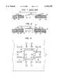
- a recessed-chip modulecomprising IC chip 11 and intermediate interconnection substrate (IIS) 12.
- the IIScan be any suitable material such as epoxy or ceramic, but is preferably silicon.
- the chip 11is flip-chip bonded to IIS 12 by interconnections 13 which are typically solder, but may be other conductive material such as conductive epoxy.
- the technique used for the flip-chip bondis not part of the invention and may e.g. be solder bump or ball bonding, or conductive epoxy etc.
- the IIS tile 12is in turn flip-bonded to printed wiring board (PWB) 14 with solder or conductive epoxy I/O interconnections 15.
- PWBprinted wiring board
- the PWB 14is provided with a cavity 15 so that the chip 11 can be recessed below the PWB surface as shown.
- the cavitymay extend through the thickness of the PWB as shown in FIG. 1, or may extend only partially through the PWB.
- the PWBis a single level board with dual side printed circuits. It could also be a multilevel PWB.
- the PWBmay be interconnected to a system printed wiring board (not shown).
- a cutaway portion of the PWBis shown to illustrate that the PWB is a portion of a larger PWB that may accommodate several IISs.
- the IIS 12may be an active device, such as a quad package, with a large array of I/O bonding sites arranged in a square or rectangular configuration at the periphery of the substrate.
- the IISmay be a passive interconnection substrate, such as silicon, with a printed circuit on one or both sides.
- the solder ball 16is bonded to a bonding pad on the PWB 14, and the pad is interconnected by runner 17 that extends to plated through hole interconnection 18, and then via runner 19 on the bottom of the PWB to another contact site (not shown).
- the other contact sitemay another bonding pad, if the PWB is to be soldered to another board, or if wire bonds are made to the PWB.
- the contact sitesmay be slot interconnections if the PWB is a plug-in circuit card.
- the interconnection shown by 16, 17, 18, and 19is a power interconnection, and the similar interconnection comprising elements 21, 22, 23, and 24 is a ground interconnection.
- the remaining I/O connectionsare not shown but are conventional.
- the interconnection in this embodimentcomprises edge connectors 31 and 32 which extend from the top of the PWB to the bottom of the PWB along the edges or sidewalls of the cavity 15. Elements common to both figures have the same reference numbers.
- Solder bump interconnections 33 and 34provide added interconnection capability to the structure.
- the solder bumps 33 and 34interconnect the IIS 12 to contact pads on the top of the PWB 14, then along plated edge connectors 31 and 32 to runners 35 and 36 on the bottom of the PWB.
- the added interconnectionsthat are made possible by using conductive plating on the edge of the cavity in a recessed chip board assembly can accommodate I/O signals but are preferably used for power and ground interconnections. This configuration allows the power and ground connections to be optimally short, and allows them to be relatively isolated from the signal runners.
- FIG. 3Another embodiment of the invention is shown in FIG. 3 where the IIS 12 is attached to a ball grid array interconnection substrate 41.
- Ball bonds 42 and 43are power and ground interconnections and ball bonds 44 and 45 comprise the I/O signal interconnections.
- the top side of interconnection substrate 41is shown in plan view in FIG. 4, with the IIS 12 removed, and the under side of the interconnection substrate is shown in FIG. 5.
- the interconnection substrate 41is adapted to be mounted on a system board (not shown).
- FIG. 4shows that with the elimination of the usual capture pads for the power and ground through hole interconnections, most of the interconnection substrate area (an enhanced area) is available for signal I/O interconnections.
- the routing arrangement shown in FIG. 4is relatively simple, i.e. each runner leads directly from the signal bump to an adjacent through hole. In other circuit designs the routing may be more complex, i.e. from a signal bump to a remote through hole. The availability of extra routing space, made possible by the cavity edge interconnections for power and ground, is a significant advantage.
- the inventionis especially useful for multi-chip module packages in which one or more of the chips are RF chips.
- RF devicesare particularly susceptible to interference from external electromagnetic fields.
- the inventionis applicable to PWB interconnection arrangements wherein the intermediate PWB has an opening that extends completely through the thickness of the board, and the MCM is mounted so as to recess significantly below the surface of the board, thus reducing the package profile.
- Such structuresare quadrangular in shape, and frequently square in shape.
- the intermediate interconnection substrate, to which the IC chips are attachedcovers the cavity so that the four edge portions extend over portions of the PWB, and ball or bump bonds are made between the intermediate interconnection substrate and the PWB.
- the IIScovers the entire cavity and all four edges overlap the PWB as viewed from above.
- structuresmay be equally effective in which only two facing edges of the IIS overlap the PWB and ball or bump bonds are made along those two facing edges.
- recessed chip packagescan be made with interconnections along only one edge of the cavity.
- the inventionis also applicable to multilayer PWBs in which the cavity extends only partially through the thickness of the PWB.
- FIG. 6where the added PWB level is shown at 61.
- the power and ground cavity edge interconnections 31 and 32comprise part of the interlevel printed circuit as shown.
- the power and ground runners in the arrangement of FIG. 6may be terminated at contact pads (not shown) on either the bottom or the top of the multilayer board.
- the term printed wiring boardis intended to include a single level board, or one level of a multilevel board.
Landscapes
- Engineering & Computer Science (AREA)
- Microelectronics & Electronic Packaging (AREA)
- Computer Hardware Design (AREA)
- Power Engineering (AREA)
- Physics & Mathematics (AREA)
- Condensed Matter Physics & Semiconductors (AREA)
- General Physics & Mathematics (AREA)
- Geometry (AREA)
- Structures For Mounting Electric Components On Printed Circuit Boards (AREA)
- Structure Of Printed Boards (AREA)
- Wire Bonding (AREA)
Abstract
Description
Claims (7)
Priority Applications (4)
| Application Number | Priority Date | Filing Date | Title |
|---|---|---|---|
| US09/120,148US6154370A (en) | 1998-07-21 | 1998-07-21 | Recessed flip-chip package |
| TW088108558ATW429565B (en) | 1998-07-21 | 1999-05-25 | Recessed flip-chip package |
| KR1019990028642AKR100310572B1 (en) | 1998-07-21 | 1999-07-15 | Recessed flip-chip package |
| JP20518199AJP3742252B2 (en) | 1998-07-21 | 1999-07-19 | IC package |
Applications Claiming Priority (1)
| Application Number | Priority Date | Filing Date | Title |
|---|---|---|---|
| US09/120,148US6154370A (en) | 1998-07-21 | 1998-07-21 | Recessed flip-chip package |
Publications (1)
| Publication Number | Publication Date |
|---|---|
| US6154370Atrue US6154370A (en) | 2000-11-28 |
Family
ID=22388537
Family Applications (1)
| Application Number | Title | Priority Date | Filing Date |
|---|---|---|---|
| US09/120,148Expired - LifetimeUS6154370A (en) | 1998-07-21 | 1998-07-21 | Recessed flip-chip package |
Country Status (4)
| Country | Link |
|---|---|
| US (1) | US6154370A (en) |
| JP (1) | JP3742252B2 (en) |
| KR (1) | KR100310572B1 (en) |
| TW (1) | TW429565B (en) |
Cited By (67)
| Publication number | Priority date | Publication date | Assignee | Title |
|---|---|---|---|---|
| US6297551B1 (en)* | 1999-09-22 | 2001-10-02 | Agere Systems Guardian Corp. | Integrated circuit packages with improved EMI characteristics |
| US6486545B1 (en)* | 2001-07-26 | 2002-11-26 | Amkor Technology, Inc. | Pre-drilled ball grid array package |
| US6489669B2 (en)* | 2000-09-11 | 2002-12-03 | Rohm Co., Ltd. | Integrated circuit device |
| US6528871B1 (en)* | 1999-07-27 | 2003-03-04 | Mitsubishi Denki Kabushiki Kaisha | Structure and method for mounting semiconductor devices |
| US20030048624A1 (en)* | 2001-08-22 | 2003-03-13 | Tessera, Inc. | Low-height multi-component assemblies |
| US6548759B1 (en) | 2001-06-28 | 2003-04-15 | Amkor Technology, Inc. | Pre-drilled image sensor package |
| US20030089998A1 (en)* | 2001-11-09 | 2003-05-15 | Chan Vincent K. | Direct interconnect multi-chip module, method for making the same and electronic package comprising same |
| WO2003003459A3 (en)* | 2001-06-27 | 2003-05-30 | Infineon Technologies Ag | Arrangement of a semiconductor component on a substrate |
| US20030127749A1 (en)* | 2000-05-19 | 2003-07-10 | Megic Corporation | Multiple chips bonded to packaging structure with low noise and multiple selectable functions |
| US6606251B1 (en) | 2002-02-07 | 2003-08-12 | Cooligy Inc. | Power conditioning module |
| US6617693B2 (en)* | 1999-02-03 | 2003-09-09 | Rohm Co., Ltd. | Semiconductor device and semiconductor chip for use therein |
| US20030213619A1 (en)* | 2002-05-14 | 2003-11-20 | Denzene Quentin S. | Ground discontinuity improvement in RF device matching |
| US20030234709A1 (en)* | 2000-09-18 | 2003-12-25 | Meder Electronic | Lead-less surface mount reed relay |
| US20040068867A1 (en)* | 2002-10-15 | 2004-04-15 | Burton Edward Allyn | Land-side mounting of components to an integrated circuit package |
| US6730536B1 (en) | 2001-06-28 | 2004-05-04 | Amkor Technology, Inc. | Pre-drilled image sensor package fabrication method |
| US20040090755A1 (en)* | 2002-11-01 | 2004-05-13 | Alps Electric Co., Ltd. | Small and securely-soldered electronic unit |
| US20040217459A1 (en)* | 2001-03-30 | 2004-11-04 | Fee Setho Sing | Ball grid array interposer, packages and methods |
| US6942018B2 (en) | 2001-09-28 | 2005-09-13 | The Board Of Trustees Of The Leland Stanford Junior University | Electroosmotic microchannel cooling system |
| US20050218518A1 (en)* | 2002-01-07 | 2005-10-06 | Tongbi Jiang | Semiconductor device assemblies and packages including multiple semiconductor device components |
| US7061102B2 (en) | 2001-06-11 | 2006-06-13 | Xilinx, Inc. | High performance flipchip package that incorporates heat removal with minimal thermal mismatch |
| US7134486B2 (en) | 2001-09-28 | 2006-11-14 | The Board Of Trustees Of The Leeland Stanford Junior University | Control of electrolysis gases in electroosmotic pump systems |
| US20070014095A1 (en)* | 2005-07-12 | 2007-01-18 | Weiss Roger E | High-performance separable electrical device/printed circuit board interconnection |
| US20070045795A1 (en)* | 2005-08-31 | 2007-03-01 | Mcbean Ronald V | MEMS package and method of forming the same |
| US20080003884A1 (en)* | 2006-06-30 | 2008-01-03 | Seagate Technology Llc | Testing a high speed serial bus within a printed circuit board |
| US7379316B2 (en) | 2005-09-02 | 2008-05-27 | Metaram, Inc. | Methods and apparatus of stacking DRAMs |
| US7386656B2 (en) | 2006-07-31 | 2008-06-10 | Metaram, Inc. | Interface circuit system and method for performing power management operations in conjunction with only a portion of a memory circuit |
| US20080142250A1 (en)* | 2006-12-18 | 2008-06-19 | Tang George C | Electronic component connection support structures including air as a dielectric |
| US7392338B2 (en) | 2006-07-31 | 2008-06-24 | Metaram, Inc. | Interface circuit system and method for autonomously performing power management operations in conjunction with a plurality of memory circuits |
| US7472220B2 (en) | 2006-07-31 | 2008-12-30 | Metaram, Inc. | Interface circuit system and method for performing power management operations utilizing power management signals |
| US7515453B2 (en) | 2005-06-24 | 2009-04-07 | Metaram, Inc. | Integrated memory core and memory interface circuit |
| US20090121335A1 (en)* | 2007-11-12 | 2009-05-14 | Zigmund Ramirez Camacho | Integrated circuit package system with package integration |
| US20090161334A1 (en)* | 2007-12-24 | 2009-06-25 | Kuo-Hsien Liao | Wireless communication module |
| US7580312B2 (en) | 2006-07-31 | 2009-08-25 | Metaram, Inc. | Power saving system and method for use with a plurality of memory circuits |
| US7581127B2 (en) | 2006-07-31 | 2009-08-25 | Metaram, Inc. | Interface circuit system and method for performing power saving operations during a command-related latency |
| US7609567B2 (en) | 2005-06-24 | 2009-10-27 | Metaram, Inc. | System and method for simulating an aspect of a memory circuit |
| US7724589B2 (en) | 2006-07-31 | 2010-05-25 | Google Inc. | System and method for delaying a signal communicated from a system to at least one of a plurality of memory circuits |
| US20110064363A1 (en)* | 2009-09-14 | 2011-03-17 | Zarlink Semiconductor Ab | Self-aligned carrier assembly for optical device supporting wafer scale methods |
| US8041881B2 (en) | 2006-07-31 | 2011-10-18 | Google Inc. | Memory device with emulated characteristics |
| US8055833B2 (en) | 2006-10-05 | 2011-11-08 | Google Inc. | System and method for increasing capacity, performance, and flexibility of flash storage |
| US8060774B2 (en) | 2005-06-24 | 2011-11-15 | Google Inc. | Memory systems and memory modules |
| US20110298064A1 (en)* | 2009-02-06 | 2011-12-08 | Epcos Ag | Sensor module and method for producing sensor modules |
| US8077535B2 (en) | 2006-07-31 | 2011-12-13 | Google Inc. | Memory refresh apparatus and method |
| US8080874B1 (en) | 2007-09-14 | 2011-12-20 | Google Inc. | Providing additional space between an integrated circuit and a circuit board for positioning a component therebetween |
| US8081474B1 (en) | 2007-12-18 | 2011-12-20 | Google Inc. | Embossed heat spreader |
| US8090897B2 (en) | 2006-07-31 | 2012-01-03 | Google Inc. | System and method for simulating an aspect of a memory circuit |
| US8089795B2 (en) | 2006-02-09 | 2012-01-03 | Google Inc. | Memory module with memory stack and interface with enhanced capabilities |
| US8111566B1 (en) | 2007-11-16 | 2012-02-07 | Google, Inc. | Optimal channel design for memory devices for providing a high-speed memory interface |
| US8130560B1 (en) | 2006-11-13 | 2012-03-06 | Google Inc. | Multi-rank partial width memory modules |
| US8169233B2 (en) | 2009-06-09 | 2012-05-01 | Google Inc. | Programming of DIMM termination resistance values |
| US8209479B2 (en) | 2007-07-18 | 2012-06-26 | Google Inc. | Memory circuit system and method |
| US8244971B2 (en) | 2006-07-31 | 2012-08-14 | Google Inc. | Memory circuit system and method |
| US8280714B2 (en) | 2006-07-31 | 2012-10-02 | Google Inc. | Memory circuit simulation system and method with refresh capabilities |
| US8327104B2 (en) | 2006-07-31 | 2012-12-04 | Google Inc. | Adjusting the timing of signals associated with a memory system |
| US8335894B1 (en) | 2008-07-25 | 2012-12-18 | Google Inc. | Configurable memory system with interface circuit |
| US8386722B1 (en) | 2008-06-23 | 2013-02-26 | Google Inc. | Stacked DIMM memory interface |
| US8397013B1 (en) | 2006-10-05 | 2013-03-12 | Google Inc. | Hybrid memory module |
| US8438328B2 (en) | 2008-02-21 | 2013-05-07 | Google Inc. | Emulation of abstracted DIMMs using abstracted DRAMs |
| US8566516B2 (en) | 2006-07-31 | 2013-10-22 | Google Inc. | Refresh management of memory modules |
| US8796830B1 (en) | 2006-09-01 | 2014-08-05 | Google Inc. | Stackable low-profile lead frame package |
| US8972673B2 (en) | 2006-07-31 | 2015-03-03 | Google Inc. | Power management of memory circuits by virtual memory simulation |
| US9171585B2 (en) | 2005-06-24 | 2015-10-27 | Google Inc. | Configurable memory circuit system and method |
| US9507739B2 (en) | 2005-06-24 | 2016-11-29 | Google Inc. | Configurable memory circuit system and method |
| US9542353B2 (en) | 2006-02-09 | 2017-01-10 | Google Inc. | System and method for reducing command scheduling constraints of memory circuits |
| WO2017039630A1 (en)* | 2015-08-31 | 2017-03-09 | Intel IP Corporation | Low thermal resistance hanging die package |
| US9632929B2 (en) | 2006-02-09 | 2017-04-25 | Google Inc. | Translating an address associated with a command communicated between a system and memory circuits |
| US10013371B2 (en) | 2005-06-24 | 2018-07-03 | Google Llc | Configurable memory circuit system and method |
| CN110759311A (en)* | 2019-10-29 | 2020-02-07 | 太极半导体(苏州)有限公司 | Leadless MEMS chip packaging structure based on window type substrate and process thereof |
Families Citing this family (1)
| Publication number | Priority date | Publication date | Assignee | Title |
|---|---|---|---|---|
| JP5177910B2 (en)* | 2010-03-23 | 2013-04-10 | パナソニック株式会社 | Semiconductor device and manufacturing method thereof |
Citations (4)
| Publication number | Priority date | Publication date | Assignee | Title |
|---|---|---|---|---|
| US5608262A (en)* | 1995-02-24 | 1997-03-04 | Lucent Technologies Inc. | Packaging multi-chip modules without wire-bond interconnection |
| US5715144A (en)* | 1994-12-30 | 1998-02-03 | International Business Machines Corporation | Multi-layer, multi-chip pyramid and circuit board structure |
| US5786986A (en)* | 1989-04-17 | 1998-07-28 | International Business Machines Corporation | Multi-level circuit card structure |
| US5869894A (en)* | 1997-07-18 | 1999-02-09 | Lucent Technologies Inc. | RF IC package |
- 1998
- 1998-07-21USUS09/120,148patent/US6154370A/ennot_activeExpired - Lifetime
- 1999
- 1999-05-25TWTW088108558Apatent/TW429565B/ennot_activeIP Right Cessation
- 1999-07-15KRKR1019990028642Apatent/KR100310572B1/ennot_activeExpired - Lifetime
- 1999-07-19JPJP20518199Apatent/JP3742252B2/ennot_activeExpired - Lifetime
Patent Citations (4)
| Publication number | Priority date | Publication date | Assignee | Title |
|---|---|---|---|---|
| US5786986A (en)* | 1989-04-17 | 1998-07-28 | International Business Machines Corporation | Multi-level circuit card structure |
| US5715144A (en)* | 1994-12-30 | 1998-02-03 | International Business Machines Corporation | Multi-layer, multi-chip pyramid and circuit board structure |
| US5608262A (en)* | 1995-02-24 | 1997-03-04 | Lucent Technologies Inc. | Packaging multi-chip modules without wire-bond interconnection |
| US5869894A (en)* | 1997-07-18 | 1999-02-09 | Lucent Technologies Inc. | RF IC package |
Cited By (117)
| Publication number | Priority date | Publication date | Assignee | Title |
|---|---|---|---|---|
| US7126226B2 (en) | 1999-02-03 | 2006-10-24 | Rohm Co., Ltd. | Semiconductor device and semiconductor chip for use therein |
| US6617693B2 (en)* | 1999-02-03 | 2003-09-09 | Rohm Co., Ltd. | Semiconductor device and semiconductor chip for use therein |
| US7045386B2 (en)* | 1999-02-03 | 2006-05-16 | Rohm Co., Ltd. | Semiconductor device and semiconductor chip for use therein |
| US20040026790A1 (en)* | 1999-02-03 | 2004-02-12 | Rohm Co., Ltd. | Semiconductor device and semiconductor chip for use therein |
| US6528871B1 (en)* | 1999-07-27 | 2003-03-04 | Mitsubishi Denki Kabushiki Kaisha | Structure and method for mounting semiconductor devices |
| US6297551B1 (en)* | 1999-09-22 | 2001-10-02 | Agere Systems Guardian Corp. | Integrated circuit packages with improved EMI characteristics |
| US8148806B2 (en) | 2000-05-19 | 2012-04-03 | Megica Corporation | Multiple chips bonded to packaging structure with low noise and multiple selectable functions |
| US20030127749A1 (en)* | 2000-05-19 | 2003-07-10 | Megic Corporation | Multiple chips bonded to packaging structure with low noise and multiple selectable functions |
| US7045901B2 (en)* | 2000-05-19 | 2006-05-16 | Megic Corporation | Chip-on-chip connection with second chip located in rectangular open window hole in printed circuit board |
| US6489669B2 (en)* | 2000-09-11 | 2002-12-03 | Rohm Co., Ltd. | Integrated circuit device |
| US20030234709A1 (en)* | 2000-09-18 | 2003-12-25 | Meder Electronic | Lead-less surface mount reed relay |
| US6954126B2 (en) | 2000-09-18 | 2005-10-11 | Meder Electronic, Inc. | Lead-less surface mount reed relay |
| US20040217459A1 (en)* | 2001-03-30 | 2004-11-04 | Fee Setho Sing | Ball grid array interposer, packages and methods |
| US7528007B2 (en) | 2001-03-30 | 2009-05-05 | Micron Technology, Inc. | Methods for assembling semiconductor devices and interposers |
| US7274095B2 (en) | 2001-03-30 | 2007-09-25 | Micron Technology, Inc. | Interposers with receptacles for receiving semiconductor devices and assemblies and packages including such interposers |
| US20060194373A1 (en)* | 2001-03-30 | 2006-08-31 | Fee Setho S | Methods for assembling semiconductor devices and interposers |
| US7061102B2 (en) | 2001-06-11 | 2006-06-13 | Xilinx, Inc. | High performance flipchip package that incorporates heat removal with minimal thermal mismatch |
| WO2003003459A3 (en)* | 2001-06-27 | 2003-05-30 | Infineon Technologies Ag | Arrangement of a semiconductor component on a substrate |
| US6730536B1 (en) | 2001-06-28 | 2004-05-04 | Amkor Technology, Inc. | Pre-drilled image sensor package fabrication method |
| US6548759B1 (en) | 2001-06-28 | 2003-04-15 | Amkor Technology, Inc. | Pre-drilled image sensor package |
| US6486545B1 (en)* | 2001-07-26 | 2002-11-26 | Amkor Technology, Inc. | Pre-drilled ball grid array package |
| US20030048624A1 (en)* | 2001-08-22 | 2003-03-13 | Tessera, Inc. | Low-height multi-component assemblies |
| US6991024B2 (en) | 2001-09-28 | 2006-01-31 | The Board Of Trustees Of The Leland Stanford Junior University | Electroosmotic microchannel cooling system |
| US7334630B2 (en) | 2001-09-28 | 2008-02-26 | The Board Of Trustees Of The Leland Stanford Junior University | Closed-loop microchannel cooling system |
| US7134486B2 (en) | 2001-09-28 | 2006-11-14 | The Board Of Trustees Of The Leeland Stanford Junior University | Control of electrolysis gases in electroosmotic pump systems |
| US6942018B2 (en) | 2001-09-28 | 2005-09-13 | The Board Of Trustees Of The Leland Stanford Junior University | Electroosmotic microchannel cooling system |
| US7131486B2 (en) | 2001-09-28 | 2006-11-07 | The Board Of Trustees Of The Leland Stanford Junior Universty | Electroosmotic microchannel cooling system |
| US20030089998A1 (en)* | 2001-11-09 | 2003-05-15 | Chan Vincent K. | Direct interconnect multi-chip module, method for making the same and electronic package comprising same |
| US20050218518A1 (en)* | 2002-01-07 | 2005-10-06 | Tongbi Jiang | Semiconductor device assemblies and packages including multiple semiconductor device components |
| US6678168B2 (en) | 2002-02-07 | 2004-01-13 | Cooligy, Inc. | System including power conditioning modules |
| US6606251B1 (en) | 2002-02-07 | 2003-08-12 | Cooligy Inc. | Power conditioning module |
| US20030213619A1 (en)* | 2002-05-14 | 2003-11-20 | Denzene Quentin S. | Ground discontinuity improvement in RF device matching |
| US7573136B2 (en)* | 2002-06-27 | 2009-08-11 | Micron Technology, Inc. | Semiconductor device assemblies and packages including multiple semiconductor device components |
| US20040068867A1 (en)* | 2002-10-15 | 2004-04-15 | Burton Edward Allyn | Land-side mounting of components to an integrated circuit package |
| EP1416778A3 (en)* | 2002-11-01 | 2006-10-11 | Alps Electric Co., Ltd. | Small and securely-soldered electronic unit |
| US20040090755A1 (en)* | 2002-11-01 | 2004-05-13 | Alps Electric Co., Ltd. | Small and securely-soldered electronic unit |
| US9171585B2 (en) | 2005-06-24 | 2015-10-27 | Google Inc. | Configurable memory circuit system and method |
| US9507739B2 (en) | 2005-06-24 | 2016-11-29 | Google Inc. | Configurable memory circuit system and method |
| US8615679B2 (en) | 2005-06-24 | 2013-12-24 | Google Inc. | Memory modules with reliability and serviceability functions |
| US7609567B2 (en) | 2005-06-24 | 2009-10-27 | Metaram, Inc. | System and method for simulating an aspect of a memory circuit |
| US8386833B2 (en) | 2005-06-24 | 2013-02-26 | Google Inc. | Memory systems and memory modules |
| US7515453B2 (en) | 2005-06-24 | 2009-04-07 | Metaram, Inc. | Integrated memory core and memory interface circuit |
| US10013371B2 (en) | 2005-06-24 | 2018-07-03 | Google Llc | Configurable memory circuit system and method |
| US8359187B2 (en) | 2005-06-24 | 2013-01-22 | Google Inc. | Simulating a different number of memory circuit devices |
| US8060774B2 (en) | 2005-06-24 | 2011-11-15 | Google Inc. | Memory systems and memory modules |
| US20070014095A1 (en)* | 2005-07-12 | 2007-01-18 | Weiss Roger E | High-performance separable electrical device/printed circuit board interconnection |
| US20070045795A1 (en)* | 2005-08-31 | 2007-03-01 | Mcbean Ronald V | MEMS package and method of forming the same |
| US8582339B2 (en) | 2005-09-02 | 2013-11-12 | Google Inc. | System including memory stacks |
| US8619452B2 (en) | 2005-09-02 | 2013-12-31 | Google Inc. | Methods and apparatus of stacking DRAMs |
| US8811065B2 (en) | 2005-09-02 | 2014-08-19 | Google Inc. | Performing error detection on DRAMs |
| US7379316B2 (en) | 2005-09-02 | 2008-05-27 | Metaram, Inc. | Methods and apparatus of stacking DRAMs |
| US9542353B2 (en) | 2006-02-09 | 2017-01-10 | Google Inc. | System and method for reducing command scheduling constraints of memory circuits |
| US8797779B2 (en) | 2006-02-09 | 2014-08-05 | Google Inc. | Memory module with memory stack and interface with enhanced capabilites |
| US9727458B2 (en) | 2006-02-09 | 2017-08-08 | Google Inc. | Translating an address associated with a command communicated between a system and memory circuits |
| US8566556B2 (en) | 2006-02-09 | 2013-10-22 | Google Inc. | Memory module with memory stack and interface with enhanced capabilities |
| US8089795B2 (en) | 2006-02-09 | 2012-01-03 | Google Inc. | Memory module with memory stack and interface with enhanced capabilities |
| US9632929B2 (en) | 2006-02-09 | 2017-04-25 | Google Inc. | Translating an address associated with a command communicated between a system and memory circuits |
| US9542352B2 (en) | 2006-02-09 | 2017-01-10 | Google Inc. | System and method for reducing command scheduling constraints of memory circuits |
| US7727004B2 (en)* | 2006-06-30 | 2010-06-01 | Seagate Technology Llc | Testing a high speed serial bus within a printed circuit board |
| US20080003884A1 (en)* | 2006-06-30 | 2008-01-03 | Seagate Technology Llc | Testing a high speed serial bus within a printed circuit board |
| US7392338B2 (en) | 2006-07-31 | 2008-06-24 | Metaram, Inc. | Interface circuit system and method for autonomously performing power management operations in conjunction with a plurality of memory circuits |
| US8244971B2 (en) | 2006-07-31 | 2012-08-14 | Google Inc. | Memory circuit system and method |
| US8090897B2 (en) | 2006-07-31 | 2012-01-03 | Google Inc. | System and method for simulating an aspect of a memory circuit |
| US8631220B2 (en) | 2006-07-31 | 2014-01-14 | Google Inc. | Adjusting the timing of signals associated with a memory system |
| US7386656B2 (en) | 2006-07-31 | 2008-06-10 | Metaram, Inc. | Interface circuit system and method for performing power management operations in conjunction with only a portion of a memory circuit |
| US9047976B2 (en) | 2006-07-31 | 2015-06-02 | Google Inc. | Combined signal delay and power saving for use with a plurality of memory circuits |
| US8041881B2 (en) | 2006-07-31 | 2011-10-18 | Google Inc. | Memory device with emulated characteristics |
| US8972673B2 (en) | 2006-07-31 | 2015-03-03 | Google Inc. | Power management of memory circuits by virtual memory simulation |
| US8154935B2 (en) | 2006-07-31 | 2012-04-10 | Google Inc. | Delaying a signal communicated from a system to at least one of a plurality of memory circuits |
| US8868829B2 (en) | 2006-07-31 | 2014-10-21 | Google Inc. | Memory circuit system and method |
| US7724589B2 (en) | 2006-07-31 | 2010-05-25 | Google Inc. | System and method for delaying a signal communicated from a system to at least one of a plurality of memory circuits |
| US8077535B2 (en) | 2006-07-31 | 2011-12-13 | Google Inc. | Memory refresh apparatus and method |
| US7580312B2 (en) | 2006-07-31 | 2009-08-25 | Metaram, Inc. | Power saving system and method for use with a plurality of memory circuits |
| US8280714B2 (en) | 2006-07-31 | 2012-10-02 | Google Inc. | Memory circuit simulation system and method with refresh capabilities |
| US8327104B2 (en) | 2006-07-31 | 2012-12-04 | Google Inc. | Adjusting the timing of signals associated with a memory system |
| US7590796B2 (en) | 2006-07-31 | 2009-09-15 | Metaram, Inc. | System and method for power management in memory systems |
| US8340953B2 (en) | 2006-07-31 | 2012-12-25 | Google, Inc. | Memory circuit simulation with power saving capabilities |
| US8566516B2 (en) | 2006-07-31 | 2013-10-22 | Google Inc. | Refresh management of memory modules |
| US7581127B2 (en) | 2006-07-31 | 2009-08-25 | Metaram, Inc. | Interface circuit system and method for performing power saving operations during a command-related latency |
| US8745321B2 (en) | 2006-07-31 | 2014-06-03 | Google Inc. | Simulating a memory standard |
| US7472220B2 (en) | 2006-07-31 | 2008-12-30 | Metaram, Inc. | Interface circuit system and method for performing power management operations utilizing power management signals |
| US8796830B1 (en) | 2006-09-01 | 2014-08-05 | Google Inc. | Stackable low-profile lead frame package |
| US8397013B1 (en) | 2006-10-05 | 2013-03-12 | Google Inc. | Hybrid memory module |
| US8370566B2 (en) | 2006-10-05 | 2013-02-05 | Google Inc. | System and method for increasing capacity, performance, and flexibility of flash storage |
| US8751732B2 (en) | 2006-10-05 | 2014-06-10 | Google Inc. | System and method for increasing capacity, performance, and flexibility of flash storage |
| US8977806B1 (en) | 2006-10-05 | 2015-03-10 | Google Inc. | Hybrid memory module |
| US8055833B2 (en) | 2006-10-05 | 2011-11-08 | Google Inc. | System and method for increasing capacity, performance, and flexibility of flash storage |
| US8446781B1 (en) | 2006-11-13 | 2013-05-21 | Google Inc. | Multi-rank partial width memory modules |
| US8130560B1 (en) | 2006-11-13 | 2012-03-06 | Google Inc. | Multi-rank partial width memory modules |
| US8760936B1 (en) | 2006-11-13 | 2014-06-24 | Google Inc. | Multi-rank partial width memory modules |
| US20080142250A1 (en)* | 2006-12-18 | 2008-06-19 | Tang George C | Electronic component connection support structures including air as a dielectric |
| US7557303B2 (en)* | 2006-12-18 | 2009-07-07 | Lsi Corporation | Electronic component connection support structures including air as a dielectric |
| US8209479B2 (en) | 2007-07-18 | 2012-06-26 | Google Inc. | Memory circuit system and method |
| US8080874B1 (en) | 2007-09-14 | 2011-12-20 | Google Inc. | Providing additional space between an integrated circuit and a circuit board for positioning a component therebetween |
| US20090121335A1 (en)* | 2007-11-12 | 2009-05-14 | Zigmund Ramirez Camacho | Integrated circuit package system with package integration |
| US8258614B2 (en)* | 2007-11-12 | 2012-09-04 | Stats Chippac Ltd. | Integrated circuit package system with package integration |
| US8111566B1 (en) | 2007-11-16 | 2012-02-07 | Google, Inc. | Optimal channel design for memory devices for providing a high-speed memory interface |
| US8675429B1 (en) | 2007-11-16 | 2014-03-18 | Google Inc. | Optimal channel design for memory devices for providing a high-speed memory interface |
| US8705240B1 (en) | 2007-12-18 | 2014-04-22 | Google Inc. | Embossed heat spreader |
| US8730670B1 (en) | 2007-12-18 | 2014-05-20 | Google Inc. | Embossed heat spreader |
| US8081474B1 (en) | 2007-12-18 | 2011-12-20 | Google Inc. | Embossed heat spreader |
| US20090161334A1 (en)* | 2007-12-24 | 2009-06-25 | Kuo-Hsien Liao | Wireless communication module |
| US8144479B2 (en)* | 2007-12-24 | 2012-03-27 | Universal Scientific Industrial Co., Ltd. | Wireless communication module |
| US8631193B2 (en) | 2008-02-21 | 2014-01-14 | Google Inc. | Emulation of abstracted DIMMS using abstracted DRAMS |
| US8438328B2 (en) | 2008-02-21 | 2013-05-07 | Google Inc. | Emulation of abstracted DIMMs using abstracted DRAMs |
| US8762675B2 (en) | 2008-06-23 | 2014-06-24 | Google Inc. | Memory system for synchronous data transmission |
| US8386722B1 (en) | 2008-06-23 | 2013-02-26 | Google Inc. | Stacked DIMM memory interface |
| US8335894B1 (en) | 2008-07-25 | 2012-12-18 | Google Inc. | Configurable memory system with interface circuit |
| US8819356B2 (en) | 2008-07-25 | 2014-08-26 | Google Inc. | Configurable multirank memory system with interface circuit |
| US9061888B2 (en)* | 2009-02-06 | 2015-06-23 | Epcos Ag | Sensor module and method for producing sensor modules |
| US20110298064A1 (en)* | 2009-02-06 | 2011-12-08 | Epcos Ag | Sensor module and method for producing sensor modules |
| US8169233B2 (en) | 2009-06-09 | 2012-05-01 | Google Inc. | Programming of DIMM termination resistance values |
| US7978940B2 (en)* | 2009-09-14 | 2011-07-12 | Tyco Electronics Services Gmbh | Self-aligned carrier assembly for optical device supporting wafer scale methods |
| US20110064363A1 (en)* | 2009-09-14 | 2011-03-17 | Zarlink Semiconductor Ab | Self-aligned carrier assembly for optical device supporting wafer scale methods |
| WO2017039630A1 (en)* | 2015-08-31 | 2017-03-09 | Intel IP Corporation | Low thermal resistance hanging die package |
| US10347558B2 (en) | 2015-08-31 | 2019-07-09 | Intel IP Corporation | Low thermal resistance hanging die package |
| CN110759311A (en)* | 2019-10-29 | 2020-02-07 | 太极半导体(苏州)有限公司 | Leadless MEMS chip packaging structure based on window type substrate and process thereof |
Also Published As
| Publication number | Publication date |
|---|---|
| JP2000049248A (en) | 2000-02-18 |
| KR20000011738A (en) | 2000-02-25 |
| KR100310572B1 (en) | 2001-11-03 |
| JP3742252B2 (en) | 2006-02-01 |
| TW429565B (en) | 2001-04-11 |
Similar Documents
| Publication | Publication Date | Title |
|---|---|---|
| US6154370A (en) | Recessed flip-chip package | |
| EP0892434B1 (en) | RF IC package | |
| US6734539B2 (en) | Stacked module package | |
| US5744862A (en) | Reduced thickness semiconductor device with IC packages mounted in openings on substrate | |
| US6678167B1 (en) | High performance multi-chip IC package | |
| US5939782A (en) | Package construction for integrated circuit chip with bypass capacitor | |
| KR100368696B1 (en) | Semiconductor device, and method for manufacturing the same | |
| US6477046B1 (en) | Ball grid array package and method using enhanced power and ground distribution circuitry | |
| US6437990B1 (en) | Multi-chip ball grid array IC packages | |
| US6365962B1 (en) | Flip-chip on flex for high performance packaging applications | |
| US6461895B1 (en) | Process for making active interposer for high performance packaging applications | |
| KR100269528B1 (en) | High performance, low cost multi-chip module package | |
| KR100209760B1 (en) | Semiconductor package and its manufacturing method | |
| US6294838B1 (en) | Multi-chip stacked package | |
| US6023097A (en) | Stacked multiple-chip module micro ball grid array packaging | |
| US6340839B1 (en) | Hybrid integrated circuit | |
| US6034425A (en) | Flat multiple-chip module micro ball grid array packaging | |
| KR20010049663A (en) | Semiconductor device | |
| US6160715A (en) | Translator for recessed flip-chip package | |
| CN115732475A (en) | Fan-out type heterogeneous chip packaging structure | |
| US6137174A (en) | Hybrid ASIC/memory module package | |
| US20040201970A1 (en) | Chip interconnection method and apparatus | |
| US20020050378A1 (en) | Double-layered multiple chip module package | |
| KR20050027384A (en) | Chip size package having rerouting pad and stack thereof | |
| US6459157B1 (en) | Semiconductor device and double-sided multi-chip package |
Legal Events
| Date | Code | Title | Description |
|---|---|---|---|
| AS | Assignment | Owner name:LUCENT TECHNOLOGIES INC., NEW JERSEY Free format text:ASSIGNMENT OF ASSIGNORS INTEREST;ASSIGNORS:DEGANI, YINON;FRYE, ROBERT CHARLES;LOW, YEE LENG;REEL/FRAME:009335/0361 Effective date:19980717 | |
| STCF | Information on status: patent grant | Free format text:PATENTED CASE | |
| FEPP | Fee payment procedure | Free format text:PAYOR NUMBER ASSIGNED (ORIGINAL EVENT CODE: ASPN); ENTITY STATUS OF PATENT OWNER: LARGE ENTITY | |
| AS | Assignment | Owner name:SILICON VALLEY BANK, CALIFORNIA Free format text:SECURITY AGREEMENT;ASSIGNOR:SYCHIP, INC.;REEL/FRAME:013305/0798 Effective date:20020920 | |
| FPAY | Fee payment | Year of fee payment:4 | |
| AS | Assignment | Owner name:SYCHIP, INC., TEXAS Free format text:RELEASE BY SECURED PARTY;ASSIGNOR:SILICON VALLEY BANK;REEL/FRAME:016547/0870 Effective date:20050415 | |
| AS | Assignment | Owner name:AGERE SYSTEMS INC., PENNSYLVANIA Free format text:ASSIGNMENT OF ASSIGNORS INTEREST;ASSIGNOR:LUCENT TECHNOLGIES INC.;REEL/FRAME:017811/0404 Effective date:20010130 | |
| FPAY | Fee payment | Year of fee payment:8 | |
| FPAY | Fee payment | Year of fee payment:12 | |
| AS | Assignment | Owner name:DEUTSCHE BANK AG NEW YORK BRANCH, AS COLLATERAL AG Free format text:PATENT SECURITY AGREEMENT;ASSIGNORS:LSI CORPORATION;AGERE SYSTEMS LLC;REEL/FRAME:032856/0031 Effective date:20140506 | |
| AS | Assignment | Owner name:AVAGO TECHNOLOGIES GENERAL IP (SINGAPORE) PTE. LTD Free format text:ASSIGNMENT OF ASSIGNORS INTEREST;ASSIGNOR:AGERE SYSTEMS LLC;REEL/FRAME:035365/0634 Effective date:20140804 | |
| AS | Assignment | Owner name:LSI CORPORATION, CALIFORNIA Free format text:TERMINATION AND RELEASE OF SECURITY INTEREST IN PATENT RIGHTS (RELEASES RF 032856-0031);ASSIGNOR:DEUTSCHE BANK AG NEW YORK BRANCH, AS COLLATERAL AGENT;REEL/FRAME:037684/0039 Effective date:20160201 Owner name:AGERE SYSTEMS LLC, PENNSYLVANIA Free format text:TERMINATION AND RELEASE OF SECURITY INTEREST IN PATENT RIGHTS (RELEASES RF 032856-0031);ASSIGNOR:DEUTSCHE BANK AG NEW YORK BRANCH, AS COLLATERAL AGENT;REEL/FRAME:037684/0039 Effective date:20160201 | |
| AS | Assignment | Owner name:BANK OF AMERICA, N.A., AS COLLATERAL AGENT, NORTH CAROLINA Free format text:PATENT SECURITY AGREEMENT;ASSIGNOR:AVAGO TECHNOLOGIES GENERAL IP (SINGAPORE) PTE. LTD.;REEL/FRAME:037808/0001 Effective date:20160201 Owner name:BANK OF AMERICA, N.A., AS COLLATERAL AGENT, NORTH Free format text:PATENT SECURITY AGREEMENT;ASSIGNOR:AVAGO TECHNOLOGIES GENERAL IP (SINGAPORE) PTE. LTD.;REEL/FRAME:037808/0001 Effective date:20160201 | |
| AS | Assignment | Owner name:AVAGO TECHNOLOGIES GENERAL IP (SINGAPORE) PTE. LTD., SINGAPORE Free format text:TERMINATION AND RELEASE OF SECURITY INTEREST IN PATENTS;ASSIGNOR:BANK OF AMERICA, N.A., AS COLLATERAL AGENT;REEL/FRAME:041710/0001 Effective date:20170119 Owner name:AVAGO TECHNOLOGIES GENERAL IP (SINGAPORE) PTE. LTD Free format text:TERMINATION AND RELEASE OF SECURITY INTEREST IN PATENTS;ASSIGNOR:BANK OF AMERICA, N.A., AS COLLATERAL AGENT;REEL/FRAME:041710/0001 Effective date:20170119 | |
| AS | Assignment | Owner name:BELL SEMICONDUCTOR, LLC, ILLINOIS Free format text:ASSIGNMENT OF ASSIGNORS INTEREST;ASSIGNORS:AVAGO TECHNOLOGIES GENERAL IP (SINGAPORE) PTE. LTD.;BROADCOM CORPORATION;REEL/FRAME:044886/0766 Effective date:20171208 | |
| AS | Assignment | Owner name:CORTLAND CAPITAL MARKET SERVICES LLC, AS COLLATERA Free format text:SECURITY INTEREST;ASSIGNORS:HILCO PATENT ACQUISITION 56, LLC;BELL SEMICONDUCTOR, LLC;BELL NORTHERN RESEARCH, LLC;REEL/FRAME:045216/0020 Effective date:20180124 | |
| AS | Assignment | Owner name:BELL NORTHERN RESEARCH, LLC, ILLINOIS Free format text:RELEASE BY SECURED PARTY;ASSIGNOR:CORTLAND CAPITAL MARKET SERVICES LLC;REEL/FRAME:059723/0382 Effective date:20220401 Owner name:BELL SEMICONDUCTOR, LLC, ILLINOIS Free format text:RELEASE BY SECURED PARTY;ASSIGNOR:CORTLAND CAPITAL MARKET SERVICES LLC;REEL/FRAME:059723/0382 Effective date:20220401 Owner name:HILCO PATENT ACQUISITION 56, LLC, ILLINOIS Free format text:RELEASE BY SECURED PARTY;ASSIGNOR:CORTLAND CAPITAL MARKET SERVICES LLC;REEL/FRAME:059723/0382 Effective date:20220401 |