US6154093A - Fast adaptive wideband power amplifier feed forward linearizer using a RLS parameter tracking algorithm - Google Patents
Fast adaptive wideband power amplifier feed forward linearizer using a RLS parameter tracking algorithmDownload PDFInfo
- Publication number
- US6154093A US6154093AUS09/053,407US5340798AUS6154093AUS 6154093 AUS6154093 AUS 6154093AUS 5340798 AUS5340798 AUS 5340798AUS 6154093 AUS6154093 AUS 6154093A
- Authority
- US
- United States
- Prior art keywords
- signal
- amplifier
- cancellation
- error
- accordance
- Prior art date
- Legal status (The legal status is an assumption and is not a legal conclusion. Google has not performed a legal analysis and makes no representation as to the accuracy of the status listed.)
- Expired - Lifetime
Links
Images


Classifications
- H—ELECTRICITY
- H03—ELECTRONIC CIRCUITRY
- H03F—AMPLIFIERS
- H03F1/00—Details of amplifiers with only discharge tubes, only semiconductor devices or only unspecified devices as amplifying elements
- H03F1/32—Modifications of amplifiers to reduce non-linear distortion
- H03F1/3223—Modifications of amplifiers to reduce non-linear distortion using feed-forward
- H03F1/3229—Modifications of amplifiers to reduce non-linear distortion using feed-forward using a loop for error extraction and another loop for error subtraction
Definitions
- This inventionrelates to a wideband power amplifier and specifically to an amplifier having a feed-forward linearizer arrangement employing digital signal processing techniques.
- RFradio frequency
- applicationspower amplifiers are employed to amplify high frequency signals. Because the RF amplifiers are biased to provide substantially high output power, they exhibit nonlinear responses to some degree. Consequently, in response to an increase in the input signal power, such RF amplifiers generate intermodulation IM components, which may have frequencies that are outside a desired frequency band.
- One solution to eliminate the consequences of the nonlinear response of the amplifieris to employ multiple amplifiers each configured to amplify a predetermined carrier signal.
- the base stationsends multiple carrier signals in accordance with time division multiple access (TDMA) modulation scheme, or in accordance with code division multiple access (CDMA) modulation scheme.
- TDMAtime division multiple access
- CDMAcode division multiple access
- Each carrier frequency in TDMAcorresponds to one of the users in a specifiable cell.
- Each pseudo-code in CDMAcorresponds to one user.
- the base stationhas to communicate with many users in the corresponding cell, the intermodulation IM components increase with the number of the users.
- the use of a separate amplifier for each carrier signalsubstantially eliminates the generation of intermodulation IM components.
- this approachis costly and may not be commercially feasible in many applications.
- FIG. 1Another approach is to employ an analog linearizer, such as 10 as illustrated in FIG. 1.
- a radio frequency signal represented by frequency components 22is fed to a power amplifier 12.
- Amplifier 12generates additional intermodulation IM frequency components 24 because of its nonlinear response characteristics.
- Signal components 22'correspond to an amplified version of signal components 22.
- the function of linearizer 10is to substantially eliminate frequency components 24, as explained in more detail below.
- Linearizer 10includes a signal cancellation circuit 26 coupled to an error cancellation circuit 28.
- Signal cancellation circuit 28has an upper branch that includes power amplifier 12, and a lower branch that provides the input signal of the linearizer to an input port of an adder 16.
- the other input port of adder 16is configured to receive the output signal generated by power amplifier 12, via an attenuator 14. As a result, the output port of adder 16 provides signal components 24', which correspond to the attenuated version of intermodulation IM frequency components 24.
- Error cancellation circuit 28also includes an upper branch that is configured to provide the output signal generated by amplifier 12 to an adder 20.
- the lower branch of error cancellation circuit 28includes an amplifier 18, which is configured to receive the attenuated intermodulation components 24'.
- Amplifier 18generates an amplified version of signal 24' which is substantially equal to intermodulation component 24.
- the output port of adder 20provides signal components 22' without the distortion caused by amplifier
- the feedforward linearizer described in FIG. 1has some disadvantages. For example, because it is based on analog circuitry, it requires substantially precise components, which may lead to higher manufacturing and maintenance costs.
- feedforward linearizeremploying digital signal processing techniques.
- speed limitationsincluding delays in convergence speeds of calculations performed by such processors, restricts the effectiveness of such feedforward linearizers.
- a feedforward linearizeris employed to amplify an input signal.
- the linearizerincludes a signal cancellation circuit and an error cancellation circuit.
- the signal cancellation circuitincludes a power amplifier that is configured to amplify the input signal.
- the output of the amplifieris adjusted by the output signal that is provided by a signal cancellation vector modulator.
- the signal provided by the vector modulatoris obtained by a recursive least square mean calculator that employs a recursive least square mean algorithm.
- a mathematical model of the power amplifieris also defined, wherein the slow varying parameters of the model are separated from the fast varying parameters of the mathematical model.
- the calculatoremploys the recursive least square mean algorithm, to calculate the coefficients of the slow varying parameter of the model.
- the input signal statisticsare also obtained based on the knowledge of the input signal characteristics, such as the modulation scheme and the input signal power.
- the fast varying parameters of the mathematical modelare then obtained based on the signal statistics.
- the calculatorconverges rapidly because it preferably tracks the slow varying parameters, and not the fast varying parameters.
- the signal cancellation adjustment signalis then obtained based on the obtained amplifier model.
- the first signal cancellation branchincludes an amplifier that is configured to receive the input signal intended to be amplified.
- the output port of the amplifieris coupled to a signal cancellation vector modulator via an attenuator.
- the output port of the vector modulatoris coupled to a signal cancellation adder.
- the other input of the signal cancellation adderis configured to receive the input signal via the second signal cancellation branch.
- the feedforward linearizeralso includes an error cancellation circuit having a first error cancellation branch and a second error cancellation branch.
- the first error cancellation branchincludes an error cancellation adder configured to receive the output signal generated by said amplifier.
- the second error cancellation branchincludes an error cancellation vector modulator adapted to receive the signal generated by the signal cancellation adder and provide an adjusted error signal.
- the output port of error cancellation modulatoris provided to an auxiliary amplifier, which in turn provides its output signal to the second input port of the error cancellation adder.
- a digital signal processoris configured to provide a gain and phase adjustment signal to the vector modulators such that the output signal of the signal cancellation adder is a signal that substantially represents the intermodulation components, and the output signal of the error cancellation adder is an amplified version of the input signal, with substantially no intermodulation components.
- the processorincludes a memory that stores a mathematical model of the amplifier.
- the coefficients of the mathematical modelare then calculated by employing a Recursive Least Square algorithm.
- the gain and phase adjustment signal ⁇ for the signal cancellation modulatoris calculated based on the coefficients and input signal statistics.
- the gain and phase adjustment signal, ⁇ , for the error cancellation modulatoris also calculated based on a Least Mean Square algorithm.
- the processorperforms its calculation based on the down converted signals corresponding to the input signal, the output signal provided by the signal cancellation adder and the output signal of the linearizer.
- FIG. 1illustrates a prior art analog feedforward linearizer.
- FIG. 2illustrates a feedforward linearizer in accordance with one embodiment of the invention.
- FIG. 3illustrates a flow diagram of the steps taken by a digital signal processor employed by the feedforward linearizer illustrated in FIG. 2 in accordance with one embodiment of the present invention.
- FIGS. 4a and 4billustrate a plot representing the learning curves of adjustment signal, ⁇ and ⁇ .
- FIGS. 5a-5billustrate the simulation results of the computations made by the signal processor in accordance with the present invention.
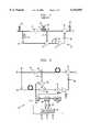
- FIG. 2illustrates a wideband power amplifier feed-forward analyzer 60 in accordance to one embodiment of the invention, although the invention is not limited in scope to this embodiment.
- Linearizer 60includes a signal cancellation circuit 86 and an error cancellation circuit 88. Each of the cancellation circuits 86 and 88 have two branches. Thus, signal cancellation circuit 86 includes a first signal cancellation branch that contains an amplifier 62, which is configured to receive an input signal V m . Input signal V m is also diverted to a second signal cancellation branch via a signal splitter 88.
- the first signal cancellation branchalso includes a signal cancellation vector modulator 66, which is configured to receive the signal generated by amplifier 62 via a splitter 90 and an attenuator 64.
- Attenuator 64may advantageously be a resistor having an attenuation r.
- An output port of vector modulator 66is coupled to an adder 68.
- the other input port of adder 68is configured to receive the input signal, V m , via the second signal cancellation branch.
- Vector modulator 66is configured to receive a signal cancellation adjustment signal, ⁇ , such that, after adjustment, the output signal, V a , generated by the amplifier is substantially orthogonal to the input signal, V m , as will be explained in more detail.
- the output port of amplifier 62is also coupled to a first error cancellation branch of linearizer 60 via signal splitter 90.
- This error cancellation branchincludes an error cancellation adder 74 adapted to receive the signal, V a , at one of its input ports.
- the second error cancellation branch of linearizer 60includes an error cancellation vector modulator 70.
- the output port of vector modulator 70is coupled to an input port of an auxiliary amplifier 72.
- the output port of auxiliary amplifier 72is coupled to the other input port of error cancellation adder 74.
- Vector modulator 70is configured to receive an error cancellation adjustment signal, ⁇ , such that after adjustment, the signal, V d , generated at the output of adder 68 is substantially orthogonal to signal, V o , generated at the output port of linearizer 60.
- a digital signal processor 76is configured to receive input signal, V m , error signal, V d , and the output signal V o .
- the digital signal processorincludes a down converter circuit 84, which is configured to shift the frequency range of signals, V m , V d and V o into the baseband frequency range, although the invention is not limited in scope in that respect.
- a separate down converter circuitin accordance with another embodiment of the invention, first shifts the frequencies to the baseband range and then provide the down converted signals to digital signal processor 76.
- the output port of down converter circuit 84is coupled to a digital signal processing circuit 80, which is configured to perform the necessary calculations to track the adjustment signals ⁇ and ⁇ .
- digital signal processing circuit 80is a dedicated processing integrated circuit chip, such as those available from Lucent Technologies, Inc, although the invention is not limited in scope in that respect.
- a memory device 78provides data information to digital signal processing circuit 80.
- the output port of digital signal processing circuit 80is coupled to a digital to analog D/A converter 82, which converts the calculated parameters to analog signals.
- the output ports of digital to analog D/A converter 82is coupled to vector modulators 66 and 70 for providing the analog versions of adjustment signals ⁇ and ⁇ respectively.
- the calculations performed by digital signal processor 76is based, among other things, on input signal statistics, as will be explained in more detail below.
- input signal statisticsIn many radio frequency applications, such as wireless communication systems, the input signal statistics change frequently and suddenly due to the traffic control and the power control.
- the optimal value of signal cancellation adjustment signal, ⁇is sensitive to the input signal statistics. Compared to adjustment signal, ⁇ , adjustment signal ⁇ is slow-varying.
- the calculation steps in accordance with the present inventionallow for a substantially fast convergence rate for determining adjustment signal, ⁇ as explained in more detail below.
- FIG. 3is a flow chart illustrating the steps accomplished by digital signal processing circuit 80 in accordance with one embodiment of the invention, although the invention is not limited in scope in that respect.
- processing circuit 80and initializes the values of ⁇ (0) and ⁇ (0).
- processing circuit 80obtains a baseband signal V bm (k) corresponding to input signal V m and retrieves a mathematical model of amplifier 62 from memory 78.
- the mathematical mode of amplifier 62is derived as explained hereinafter. Assuming that amplifier 62 has a memory in time up to ⁇ mem , the amplifier output signal, V a can be expressed as
- Equation (2)can be written as ##EQU1## wherein, i denotes the non-linear order, j denotes the memory in time, and CTs denote the cross terms, which in accordance with one embodiment of the invention may be ignored.
- samples of baseband signals of V m , and V amay be represented as V bm (k) and V ba (k) respectively, at the central frequency ⁇ .
- equation (3)may be written as ##EQU2## wherein C i 2i-1 denotes the binomial coefficient, and d 2i-1j denote the odd order coefficients of the amplifier's mathematical model. It is noted that the accuracy of the mathematical model is specifiable by determining the number of necessary terms that are included in the calculation of equation (4).
- a finite number of coefficients, a 1 2i-1jis employed to represent the coefficients of the mathematical model of amplifier 62.
- signal processing circuit 80also obtains a corresponding input signal sample V bm (k) to employ in calculations of equation (4).
- baseband signal V bd (k),corresponding to error signal, V ddis obtained.
- V ba (k)is also calculated by obtaining ##EQU3## at step 124.
- signal processing circuit 80employs a recursive algorithm known as recursive least square, RLS, algorithm to solve equation (4) based on measured samples of V bm and V ba to adaptively obtain the coefficients "a 2i-i ,-j " of the model that represents the operating point of amplifier 62.
- the RLS algorithmis well known and described, for example, in Haykin, S. Adaptive Filter Theory, 3rd. Ed. (Prentice Hall, 1996), and incorporated herein by reference.
- signal processing circuit 80obtains the input signal statistics as explained in more detail below.
- the signal cancellation adjustment signal, ⁇can be then obtained at step 130 based on the recursive calculations of amplifier coefficients "a 2i-1 .-j " and input signal statistics as ##EQU4## wherein the input signal statistics is defined in terms of the correlation ⁇ ij , between input signal, V bm , and the output signal of amplifier 62, V ba , and can be written as ##EQU5## where E(.) denotes the expectation value over time and V* bm is the complex conjugate of the input signal V bm .
- ⁇ ijis a measure of the amount of input signal components, V m in the output signal V a of the amplifier.
- parameter ⁇adjusts the output signal, V a , of amplifier 62 so that the signal component in V a , that is statistically correlated to input signal V m is substantially canceled in the error cancellation loop 86.
- ⁇ ijcan be calculated based, among other things, on the input signal power and the modulation scheme.
- the input signal power provided to amplifier 62depends, among other things, on the number of users that require servicing, and the modulation scheme may be an appropriate pulse-shaping function such as a sinusoid, although the invention is not limited in scope in that respect.
- various pulse shaping functionsmay be employed such as those discussed in Schwartz, Information Transmission, Modulation, And Noise, 3rd Ed. (McGraw Hill (1980).
- V bmcan be written as ##EQU6## wherein d is the index corresponding to the users, P d is the root mean squared power of the signal intended for the d th user, g(h) is the discrete pulse-shaping function of the modulation scheme, after sampling, ⁇ Sd ⁇ is the data sequence of the d th user, and l is the length of the pulse shaping function.
- the numerator of ⁇ ijcan be similarly simplified so that ##EQU8## therefore, ##EQU9## It will be appreciated by those skilled in the art that the term q i-2 (0) q (mj) in equation (10) is advantageously precalculated by signal processing circuit 80 (FIG. 2) in accordance with one embodiment of the present invention, based on the prior knowledge of pulse-shaping functions applied to input signals.
- digital signal processor 76provides the calculated adjustment signal a to vector modulator 66 in FIG. 2.
- signal processing circuit 80waits until the coefficients of amplifier model and the corresponding a have been stabilized. Thereafter, at step 135, baseband signal V bd and V 0 are obtained. At step 136 is performed to obtain the error cancellation adjustment signal ⁇ as described hereinafter.
- the value of signal ⁇is adaptively adjusted to be equal to r/h, wherein r is the attenuation factor provided by attenuator 64 (FIG. 2) and h is the amplification factor of auxiliary amplifier 72 (FIG. 2). Both the attenuator and the auxiliary amplifier exhibit a substantially linear response, and as such respond independently from input signal statistics.
- adjustment signal, ⁇is substantially insensitive to the fast-varying signal statistics and is deemed capable to tolerate a slower convergence algorithm, such as Least Mean Square algorithm for its derivation.
- ⁇is updated by
- ⁇is the step-size employed in the calculations in accordance with the Least Mean Square, LMS, algorithm and V bo (k is the sampled baseband signal of V o . It is noted that ⁇ is intended to modulate the error signal, V d , so that it has substantially no correlation with output signal V o .
- the value of ⁇is applied to modulator 70 in accordance with one embodiment of the invention. Steps 135 through 138 are repeated thereafter.
- FIGS. 4 and 5are plots of simulation results to illustrate the convergence speed of linearizer 60 in accordance with one embodiment of the present invention.
- the input signalconsists of four tones with unit amplitude which are place 600 k Hz apart.
- the input signalconsists of eight tones with unit amplitude which are placed 300 kHz apart.
- the center frequencyis at 900 MHZ. Temperature and other environmental factors are assumed to be constant around sample zero.
- FIG. 4(a)illustrates the power spectrum of amplifier 62 output signal, V a
- FIG. 4(b)illustrates the power spectrum of output signal, V o , respectively, long after convergence.
- FIGS. 5(a) and 5(b)illustrates the convergence curve and the absolute value of the adjustment signals, ⁇ and ⁇ , respectively. Because, the adaptation of adjustment signal, ⁇ is independent of the variations of the input signal statistics, the value of ⁇ as illustrated in FIG. 5(a) converges rather immediately, and the value of adjustment signal, ⁇ remains unchanged.
- a feedforward linearizerthat exhibits a substantially fast convergence speed.
- the signal cancellation adjustment signal, ⁇is obtained based on apriori knowledge of input signal statistics and a mathematical model of amplifier 62. Furthermore, because the signal cancellation vector modulator is located after the amplifier, the calculation of ⁇ formed by signal processing circuit 80 is only required to solve a simple linear equation, which results in equation (5). Otherwise, a non-linear equation needs to be solved.
Landscapes
- Physics & Mathematics (AREA)
- Nonlinear Science (AREA)
- Engineering & Computer Science (AREA)
- Power Engineering (AREA)
- Amplifiers (AREA)
Abstract
Description
V.sub.a (t)=ζ(V.sub.m ([t-τ.sub.mem,t])) (1)
V.sub.a (t)=G(V.sub.m (t),V.sub.m (t-mT),V.sub.m (t-2mT), . . . )(2)
β(k)=β(k-1)+μV.sub.o (k)V*.sub.d (k) (11)
Claims (17)
Priority Applications (4)
| Application Number | Priority Date | Filing Date | Title |
|---|---|---|---|
| US09/053,407US6154093A (en) | 1998-04-01 | 1998-04-01 | Fast adaptive wideband power amplifier feed forward linearizer using a RLS parameter tracking algorithm |
| DE69935942TDE69935942T2 (en) | 1998-04-01 | 1999-03-22 | Forward-controlled linearizer of a fast adaptive broadband power amplifier using RLS parameter tracking algorithms |
| EP99302191AEP0951139B1 (en) | 1998-04-01 | 1999-03-22 | Fast adaptive wideband power amplifier feed forward linearizer using a RLS parameter tracking alogrithm |
| JP09449299AJP3443539B2 (en) | 1998-04-01 | 1999-04-01 | Feedforward linearizer |
Applications Claiming Priority (1)
| Application Number | Priority Date | Filing Date | Title |
|---|---|---|---|
| US09/053,407US6154093A (en) | 1998-04-01 | 1998-04-01 | Fast adaptive wideband power amplifier feed forward linearizer using a RLS parameter tracking algorithm |
Publications (1)
| Publication Number | Publication Date |
|---|---|
| US6154093Atrue US6154093A (en) | 2000-11-28 |
Family
ID=21984015
Family Applications (1)
| Application Number | Title | Priority Date | Filing Date |
|---|---|---|---|
| US09/053,407Expired - LifetimeUS6154093A (en) | 1998-04-01 | 1998-04-01 | Fast adaptive wideband power amplifier feed forward linearizer using a RLS parameter tracking algorithm |
Country Status (4)
| Country | Link |
|---|---|
| US (1) | US6154093A (en) |
| EP (1) | EP0951139B1 (en) |
| JP (1) | JP3443539B2 (en) |
| DE (1) | DE69935942T2 (en) |
Cited By (18)
| Publication number | Priority date | Publication date | Assignee | Title |
|---|---|---|---|---|
| US6748216B1 (en)* | 1991-04-02 | 2004-06-08 | Cellco Partnership | Method and apparatus for intelligent microcell and antenna selection in digital cellular telephone systems |
| US20040119534A1 (en)* | 2002-12-18 | 2004-06-24 | Andrew Corporation, A Delaware Corporation | Model-based feed-forward linearization of amplifiers |
| US20040125885A1 (en)* | 2002-12-27 | 2004-07-01 | Roger Branson | Intermodulation product cancellation in communications |
| US20040127183A1 (en)* | 2002-12-27 | 2004-07-01 | Roger Branson | Intermodulation product cancellation in communications |
| US7184723B2 (en) | 2004-10-22 | 2007-02-27 | Parkervision, Inc. | Systems and methods for vector power amplification |
| US7355470B2 (en) | 2006-04-24 | 2008-04-08 | Parkervision, Inc. | Systems and methods of RF power transmission, modulation, and amplification, including embodiments for amplifier class transitioning |
| US7620129B2 (en) | 2007-01-16 | 2009-11-17 | Parkervision, Inc. | RF power transmission, modulation, and amplification, including embodiments for generating vector modulation control signals |
| US7885682B2 (en) | 2006-04-24 | 2011-02-08 | Parkervision, Inc. | Systems and methods of RF power transmission, modulation, and amplification, including architectural embodiments of same |
| US7911272B2 (en) | 2007-06-19 | 2011-03-22 | Parkervision, Inc. | Systems and methods of RF power transmission, modulation, and amplification, including blended control embodiments |
| US8013675B2 (en) | 2007-06-19 | 2011-09-06 | Parkervision, Inc. | Combiner-less multiple input single output (MISO) amplification with blended control |
| US8031804B2 (en) | 2006-04-24 | 2011-10-04 | Parkervision, Inc. | Systems and methods of RF tower transmission, modulation, and amplification, including embodiments for compensating for waveform distortion |
| US8315336B2 (en) | 2007-05-18 | 2012-11-20 | Parkervision, Inc. | Systems and methods of RF power transmission, modulation, and amplification, including a switching stage embodiment |
| US8334722B2 (en) | 2007-06-28 | 2012-12-18 | Parkervision, Inc. | Systems and methods of RF power transmission, modulation and amplification |
| US8755454B2 (en) | 2011-06-02 | 2014-06-17 | Parkervision, Inc. | Antenna control |
| US9106316B2 (en) | 2005-10-24 | 2015-08-11 | Parkervision, Inc. | Systems and methods of RF power transmission, modulation, and amplification |
| US9608677B2 (en) | 2005-10-24 | 2017-03-28 | Parker Vision, Inc | Systems and methods of RF power transmission, modulation, and amplification |
| US10278131B2 (en) | 2013-09-17 | 2019-04-30 | Parkervision, Inc. | Method, apparatus and system for rendering an information bearing function of time |
| KR102080202B1 (en)* | 2019-08-23 | 2020-02-21 | 주식회사 패러다임 | Power Amplifier |
Families Citing this family (2)
| Publication number | Priority date | Publication date | Assignee | Title |
|---|---|---|---|---|
| US6259319B1 (en)* | 1999-08-19 | 2001-07-10 | Lucent Technologies Inc. | Adaptive gain and/or phase adjustment control system and method |
| SE0201686L (en)* | 2002-06-04 | 2003-12-05 | Totalfoersvarets Forskningsins | Improved method for fast frequency determination using the RLS method |
Citations (8)
| Publication number | Priority date | Publication date | Assignee | Title |
|---|---|---|---|---|
| US5049832A (en)* | 1990-04-20 | 1991-09-17 | Simon Fraser University | Amplifier linearization by adaptive predistortion |
| EP0675594A1 (en)* | 1994-03-31 | 1995-10-04 | NEC Corporation | Feedforward amplifier with reduced distortion in wide band |
| US5489875A (en)* | 1994-09-21 | 1996-02-06 | Simon Fraser University | Adaptive feedforward linearizer for RF power amplifiers |
| US5508657A (en)* | 1995-01-30 | 1996-04-16 | Aml Communications, Inc. | Feed forward cancellation amplifier utilizing dynamic vector control |
| EP0729228A1 (en)* | 1995-02-22 | 1996-08-28 | STMicroelectronics S.r.l. | Basic cell for programmable analog time continuous filter |
| US5617061A (en)* | 1994-08-31 | 1997-04-01 | Nec Corporation | Feed-forward amplifier |
| US5789976A (en)* | 1996-06-17 | 1998-08-04 | Corporation De L'ecole Polytechnique | Digital adaptive control of feedforward amplifier using frequency domain cancellation |
| US5808512A (en)* | 1997-01-31 | 1998-09-15 | Ophir Rf, Inc. | Feed forward amplifiers and methods |
- 1998
- 1998-04-01USUS09/053,407patent/US6154093A/ennot_activeExpired - Lifetime
- 1999
- 1999-03-22EPEP99302191Apatent/EP0951139B1/ennot_activeExpired - Lifetime
- 1999-03-22DEDE69935942Tpatent/DE69935942T2/ennot_activeExpired - Lifetime
- 1999-04-01JPJP09449299Apatent/JP3443539B2/ennot_activeExpired - Fee Related
Patent Citations (8)
| Publication number | Priority date | Publication date | Assignee | Title |
|---|---|---|---|---|
| US5049832A (en)* | 1990-04-20 | 1991-09-17 | Simon Fraser University | Amplifier linearization by adaptive predistortion |
| EP0675594A1 (en)* | 1994-03-31 | 1995-10-04 | NEC Corporation | Feedforward amplifier with reduced distortion in wide band |
| US5617061A (en)* | 1994-08-31 | 1997-04-01 | Nec Corporation | Feed-forward amplifier |
| US5489875A (en)* | 1994-09-21 | 1996-02-06 | Simon Fraser University | Adaptive feedforward linearizer for RF power amplifiers |
| US5508657A (en)* | 1995-01-30 | 1996-04-16 | Aml Communications, Inc. | Feed forward cancellation amplifier utilizing dynamic vector control |
| EP0729228A1 (en)* | 1995-02-22 | 1996-08-28 | STMicroelectronics S.r.l. | Basic cell for programmable analog time continuous filter |
| US5789976A (en)* | 1996-06-17 | 1998-08-04 | Corporation De L'ecole Polytechnique | Digital adaptive control of feedforward amplifier using frequency domain cancellation |
| US5808512A (en)* | 1997-01-31 | 1998-09-15 | Ophir Rf, Inc. | Feed forward amplifiers and methods |
Non-Patent Citations (5)
| Title |
|---|
| Cavers, J.K. "Adaption behavior of a feedforward amplifier linearizer," IEEE Trans. on Veh. Tech., Feb. 1995, vol. 44, No. 1, pp. 31-40. |
| Cavers, J.K. Adaption behavior of a feedforward amplifier linearizer, IEEE Trans. on Veh. Tech., Feb. 1995, vol. 44, No. 1, pp. 31 40.* |
| European Search Report for Application No. 99301791 dated Jun. 30, 1999.* |
| Grant, S.J., et al., "A DSP controlled adaptive feedforward amplifier linearizer," 5th International Conference on Universal Personal Communications, Cambridge. MA, vol. 2, pp. 788-792. |
| Grant, S.J., et al., A DSP controlled adaptive feedforward amplifier linearizer, 5th International Conference on Universal Personal Communications, Cambridge. MA, vol. 2, pp. 788 792.* |
Cited By (71)
| Publication number | Priority date | Publication date | Assignee | Title |
|---|---|---|---|---|
| US6748216B1 (en)* | 1991-04-02 | 2004-06-08 | Cellco Partnership | Method and apparatus for intelligent microcell and antenna selection in digital cellular telephone systems |
| US20040119534A1 (en)* | 2002-12-18 | 2004-06-24 | Andrew Corporation, A Delaware Corporation | Model-based feed-forward linearization of amplifiers |
| US6765440B2 (en) | 2002-12-18 | 2004-07-20 | Andrew Corporation | Model-based feed-forward linearization of amplifiers |
| US7313370B2 (en) | 2002-12-27 | 2007-12-25 | Nokia Siemens Networks Oy | Intermodulation product cancellation in communications |
| US20040125885A1 (en)* | 2002-12-27 | 2004-07-01 | Roger Branson | Intermodulation product cancellation in communications |
| US20040127183A1 (en)* | 2002-12-27 | 2004-07-01 | Roger Branson | Intermodulation product cancellation in communications |
| US8781418B2 (en) | 2004-10-22 | 2014-07-15 | Parkervision, Inc. | Power amplification based on phase angle controlled reference signal and amplitude control signal |
| US8639196B2 (en) | 2004-10-22 | 2014-01-28 | Parkervision, Inc. | Control modules |
| US9768733B2 (en) | 2004-10-22 | 2017-09-19 | Parker Vision, Inc. | Multiple input single output device with vector signal and bias signal inputs |
| US8406711B2 (en) | 2004-10-22 | 2013-03-26 | Parkervision, Inc. | Systems and methods of RF power transmission, modulation, and amplification, including a Cartesian-Polar-Cartesian-Polar (CPCP) embodiment |
| US8351870B2 (en) | 2004-10-22 | 2013-01-08 | Parkervision, Inc. | Systems and methods of RF power transmission, modulation, and amplification, including cartesian 4-branch embodiments |
| US7421036B2 (en) | 2004-10-22 | 2008-09-02 | Parkervision, Inc. | Systems and methods of RF power transmission, modulation, and amplification, including transfer function embodiments |
| US8433264B2 (en) | 2004-10-22 | 2013-04-30 | Parkervision, Inc. | Multiple input single output (MISO) amplifier having multiple transistors whose output voltages substantially equal the amplifier output voltage |
| US7466760B2 (en) | 2004-10-22 | 2008-12-16 | Parkervision, Inc. | Systems and methods of RF power transmission, modulation, and amplification, including transfer function embodiments |
| US7526261B2 (en) | 2004-10-22 | 2009-04-28 | Parkervision, Inc. | RF power transmission, modulation, and amplification, including cartesian 4-branch embodiments |
| US8447248B2 (en) | 2004-10-22 | 2013-05-21 | Parkervision, Inc. | RF power transmission, modulation, and amplification, including power control of multiple input single output (MISO) amplifiers |
| US7639072B2 (en) | 2004-10-22 | 2009-12-29 | Parkervision, Inc. | Controlling a power amplifier to transition among amplifier operational classes according to at least an output signal waveform trajectory |
| US7647030B2 (en) | 2004-10-22 | 2010-01-12 | Parkervision, Inc. | Multiple input single output (MISO) amplifier with circuit branch output tracking |
| US7672650B2 (en) | 2004-10-22 | 2010-03-02 | Parkervision, Inc. | Systems and methods of RF power transmission, modulation, and amplification, including multiple input single output (MISO) amplifier embodiments comprising harmonic control circuitry |
| US9197163B2 (en) | 2004-10-22 | 2015-11-24 | Parkvision, Inc. | Systems, and methods of RF power transmission, modulation, and amplification, including embodiments for output stage protection |
| US7835709B2 (en) | 2004-10-22 | 2010-11-16 | Parkervision, Inc. | RF power transmission, modulation, and amplification using multiple input single output (MISO) amplifiers to process phase angle and magnitude information |
| US7844235B2 (en) | 2004-10-22 | 2010-11-30 | Parkervision, Inc. | RF power transmission, modulation, and amplification, including harmonic control embodiments |
| US9197164B2 (en) | 2004-10-22 | 2015-11-24 | Parkervision, Inc. | RF power transmission, modulation, and amplification, including direct cartesian 2-branch embodiments |
| US9166528B2 (en) | 2004-10-22 | 2015-10-20 | Parkervision, Inc. | RF power transmission, modulation, and amplification embodiments |
| US9143088B2 (en) | 2004-10-22 | 2015-09-22 | Parkervision, Inc. | Control modules |
| US7932776B2 (en) | 2004-10-22 | 2011-04-26 | Parkervision, Inc. | RF power transmission, modulation, and amplification embodiments |
| US8280321B2 (en) | 2004-10-22 | 2012-10-02 | Parkervision, Inc. | Systems and methods of RF power transmission, modulation, and amplification, including Cartesian-Polar-Cartesian-Polar (CPCP) embodiments |
| US7945224B2 (en) | 2004-10-22 | 2011-05-17 | Parkervision, Inc. | Systems and methods of RF power transmission, modulation, and amplification, including waveform distortion compensation embodiments |
| US8233858B2 (en) | 2004-10-22 | 2012-07-31 | Parkervision, Inc. | RF power transmission, modulation, and amplification embodiments, including control circuitry for controlling power amplifier output stages |
| US8913974B2 (en) | 2004-10-22 | 2014-12-16 | Parkervision, Inc. | RF power transmission, modulation, and amplification, including direct cartesian 2-branch embodiments |
| US8428527B2 (en) | 2004-10-22 | 2013-04-23 | Parkervision, Inc. | RF power transmission, modulation, and amplification, including direct cartesian 2-branch embodiments |
| US7327803B2 (en) | 2004-10-22 | 2008-02-05 | Parkervision, Inc. | Systems and methods for vector power amplification |
| US8626093B2 (en) | 2004-10-22 | 2014-01-07 | Parkervision, Inc. | RF power transmission, modulation, and amplification embodiments |
| US7184723B2 (en) | 2004-10-22 | 2007-02-27 | Parkervision, Inc. | Systems and methods for vector power amplification |
| US8577313B2 (en) | 2004-10-22 | 2013-11-05 | Parkervision, Inc. | Systems and methods of RF power transmission, modulation, and amplification, including output stage protection circuitry |
| US9094085B2 (en) | 2005-10-24 | 2015-07-28 | Parkervision, Inc. | Control of MISO node |
| US9106316B2 (en) | 2005-10-24 | 2015-08-11 | Parkervision, Inc. | Systems and methods of RF power transmission, modulation, and amplification |
| US9419692B2 (en) | 2005-10-24 | 2016-08-16 | Parkervision, Inc. | Antenna control |
| US9608677B2 (en) | 2005-10-24 | 2017-03-28 | Parker Vision, Inc | Systems and methods of RF power transmission, modulation, and amplification |
| US9614484B2 (en) | 2005-10-24 | 2017-04-04 | Parkervision, Inc. | Systems and methods of RF power transmission, modulation, and amplification, including control functions to transition an output of a MISO device |
| US9705540B2 (en) | 2005-10-24 | 2017-07-11 | Parker Vision, Inc. | Control of MISO node |
| US8050353B2 (en) | 2006-04-24 | 2011-11-01 | Parkervision, Inc. | Systems and methods of RF power transmission, modulation, and amplification, including embodiments for compensating for waveform distortion |
| US7750733B2 (en) | 2006-04-24 | 2010-07-06 | Parkervision, Inc. | Systems and methods of RF power transmission, modulation, and amplification, including embodiments for extending RF transmission bandwidth |
| US7355470B2 (en) | 2006-04-24 | 2008-04-08 | Parkervision, Inc. | Systems and methods of RF power transmission, modulation, and amplification, including embodiments for amplifier class transitioning |
| US7378902B2 (en) | 2006-04-24 | 2008-05-27 | Parkervision, Inc | Systems and methods of RF power transmission, modulation, and amplification, including embodiments for gain and phase control |
| US7414469B2 (en) | 2006-04-24 | 2008-08-19 | Parkervision, Inc. | Systems and methods of RF power transmission, modulation, and amplification, including embodiments for amplifier class transitioning |
| US7423477B2 (en) | 2006-04-24 | 2008-09-09 | Parkervision, Inc. | Systems and methods of RF power transmission, modulation, and amplification, including embodiments for amplifier class transitioning |
| US7885682B2 (en) | 2006-04-24 | 2011-02-08 | Parkervision, Inc. | Systems and methods of RF power transmission, modulation, and amplification, including architectural embodiments of same |
| US8059749B2 (en) | 2006-04-24 | 2011-11-15 | Parkervision, Inc. | Systems and methods of RF power transmission, modulation, and amplification, including embodiments for compensating for waveform distortion |
| US8036306B2 (en) | 2006-04-24 | 2011-10-11 | Parkervision, Inc. | Systems and methods of RF power transmission, modulation and amplification, including embodiments for compensating for waveform distortion |
| US8031804B2 (en) | 2006-04-24 | 2011-10-04 | Parkervision, Inc. | Systems and methods of RF tower transmission, modulation, and amplification, including embodiments for compensating for waveform distortion |
| US7929989B2 (en) | 2006-04-24 | 2011-04-19 | Parkervision, Inc. | Systems and methods of RF power transmission, modulation, and amplification, including architectural embodiments of same |
| US9106500B2 (en) | 2006-04-24 | 2015-08-11 | Parkervision, Inc. | Systems and methods of RF power transmission, modulation, and amplification, including embodiments for error correction |
| US8026764B2 (en) | 2006-04-24 | 2011-09-27 | Parkervision, Inc. | Generation and amplification of substantially constant envelope signals, including switching an output among a plurality of nodes |
| US7937106B2 (en) | 2006-04-24 | 2011-05-03 | ParkerVision, Inc, | Systems and methods of RF power transmission, modulation, and amplification, including architectural embodiments of same |
| US7949365B2 (en) | 2006-04-24 | 2011-05-24 | Parkervision, Inc. | Systems and methods of RF power transmission, modulation, and amplification, including architectural embodiments of same |
| US8913691B2 (en) | 2006-08-24 | 2014-12-16 | Parkervision, Inc. | Controlling output power of multiple-input single-output (MISO) device |
| US7620129B2 (en) | 2007-01-16 | 2009-11-17 | Parkervision, Inc. | RF power transmission, modulation, and amplification, including embodiments for generating vector modulation control signals |
| US8548093B2 (en) | 2007-05-18 | 2013-10-01 | Parkervision, Inc. | Power amplification based on frequency control signal |
| US8315336B2 (en) | 2007-05-18 | 2012-11-20 | Parkervision, Inc. | Systems and methods of RF power transmission, modulation, and amplification, including a switching stage embodiment |
| US8766717B2 (en) | 2007-06-19 | 2014-07-01 | Parkervision, Inc. | Systems and methods of RF power transmission, modulation, and amplification, including varying weights of control signals |
| US7911272B2 (en) | 2007-06-19 | 2011-03-22 | Parkervision, Inc. | Systems and methods of RF power transmission, modulation, and amplification, including blended control embodiments |
| US8410849B2 (en) | 2007-06-19 | 2013-04-02 | Parkervision, Inc. | Systems and methods of RF power transmission, modulation, and amplification, including blended control embodiments |
| US8502600B2 (en) | 2007-06-19 | 2013-08-06 | Parkervision, Inc. | Combiner-less multiple input single output (MISO) amplification with blended control |
| US8461924B2 (en) | 2007-06-19 | 2013-06-11 | Parkervision, Inc. | Systems and methods of RF power transmission, modulation, and amplification, including embodiments for controlling a transimpedance node |
| US8013675B2 (en) | 2007-06-19 | 2011-09-06 | Parkervision, Inc. | Combiner-less multiple input single output (MISO) amplification with blended control |
| US8884694B2 (en) | 2007-06-28 | 2014-11-11 | Parkervision, Inc. | Systems and methods of RF power transmission, modulation, and amplification |
| US8334722B2 (en) | 2007-06-28 | 2012-12-18 | Parkervision, Inc. | Systems and methods of RF power transmission, modulation and amplification |
| US8755454B2 (en) | 2011-06-02 | 2014-06-17 | Parkervision, Inc. | Antenna control |
| US10278131B2 (en) | 2013-09-17 | 2019-04-30 | Parkervision, Inc. | Method, apparatus and system for rendering an information bearing function of time |
| KR102080202B1 (en)* | 2019-08-23 | 2020-02-21 | 주식회사 패러다임 | Power Amplifier |
Also Published As
| Publication number | Publication date |
|---|---|
| EP0951139B1 (en) | 2007-05-02 |
| JP3443539B2 (en) | 2003-09-02 |
| DE69935942D1 (en) | 2007-06-14 |
| DE69935942T2 (en) | 2008-01-10 |
| EP0951139A2 (en) | 1999-10-20 |
| EP0951139A3 (en) | 2000-05-31 |
| JP2000031749A (en) | 2000-01-28 |
Similar Documents
| Publication | Publication Date | Title |
|---|---|---|
| US6154093A (en) | Fast adaptive wideband power amplifier feed forward linearizer using a RLS parameter tracking algorithm | |
| KR100338230B1 (en) | Adaptive digital predistortion linearization and feed-forward correction of rf power amplifier | |
| US6577192B2 (en) | Predistortion-type distortion compensation amplifying apparatus | |
| Hilborn et al. | An adaptive direct conversion transmitter | |
| US7460613B2 (en) | Digital linearization circuit | |
| JP3772031B2 (en) | Amplifier predistorter and amplifier | |
| US4878030A (en) | Linearizer for microwave amplifier | |
| EP1463198B1 (en) | High-efficiency linear power amplifier | |
| EP0881807B1 (en) | Tansmitter with linearised amplifier | |
| US6118335A (en) | Method and apparatus for providing adaptive predistortion in power amplifier and base station utilizing same | |
| US8150336B2 (en) | Apparatus and method for adaptive polar transmitter linearization and wireless transmitter employing the same | |
| KR100959032B1 (en) | Frequency-dependent magnitude predistortion to reduce spurious emissions in communication networks | |
| EP1560329A1 (en) | Digital predistorter using power series model | |
| US20040257157A1 (en) | Non-linear modeling method | |
| EP1085668A2 (en) | A method and apparatus for reducing adjacent channel power in wireless communication systems | |
| US20050123066A1 (en) | Adaptive pre-distortion method and apparatus for digital rf transmitters | |
| JP2000031748A (en) | Feedforward linearization device | |
| EP2525488A1 (en) | Amplifying device and signal processing device | |
| CN100440727C (en) | Distortion compensation device | |
| US6275105B1 (en) | Adaptive linearization of a feedforward amplifier by complex gain stabilization of the error amplifier | |
| KR20020008456A (en) | Base station transmit unit with feed-forward mode linearization unit | |
| WO2003003562A2 (en) | Decorrelated power amplifier linearizers | |
| KR100768684B1 (en) | Cartesian loop transmitter and method of adjusting an output level of such transmitter | |
| JPH11154880A (en) | Signal correction method and device, distortion compensation device, distortion compensation data creation device, and transmitter | |
| US6172565B1 (en) | Adaptive joint linearization, equalization and delay alignment for a wideband power amplifier |
Legal Events
| Date | Code | Title | Description |
|---|---|---|---|
| AS | Assignment | Owner name:LUCENT TECHNOLOGIES INC., NEW JERSEY Free format text:ASSIGNMENT OF ASSIGNORS INTEREST;ASSIGNORS:CHEN, JIUNN-TSAIR;CHEN, YOUNG-KAI;TSAIR, HUAN-SHANG;REEL/FRAME:009321/0439 Effective date:19980617 | |
| STCF | Information on status: patent grant | Free format text:PATENTED CASE | |
| FEPP | Fee payment procedure | Free format text:PAYOR NUMBER ASSIGNED (ORIGINAL EVENT CODE: ASPN); ENTITY STATUS OF PATENT OWNER: LARGE ENTITY | |
| AS | Assignment | Owner name:THE CHASE MANHATTAN BANK, AS COLLATERAL AGENT, TEX Free format text:CONDITIONAL ASSIGNMENT OF AND SECURITY INTEREST IN PATENT RIGHTS;ASSIGNOR:LUCENT TECHNOLOGIES INC. (DE CORPORATION);REEL/FRAME:011722/0048 Effective date:20010222 | |
| FEPP | Fee payment procedure | Free format text:PAYER NUMBER DE-ASSIGNED (ORIGINAL EVENT CODE: RMPN); ENTITY STATUS OF PATENT OWNER: LARGE ENTITY Free format text:PAYOR NUMBER ASSIGNED (ORIGINAL EVENT CODE: ASPN); ENTITY STATUS OF PATENT OWNER: LARGE ENTITY | |
| FPAY | Fee payment | Year of fee payment:4 | |
| AS | Assignment | Owner name:LUCENT TECHNOLOGIES INC., NEW JERSEY Free format text:TERMINATION AND RELEASE OF SECURITY INTEREST IN PATENT RIGHTS;ASSIGNOR:JPMORGAN CHASE BANK, N.A. (FORMERLY KNOWN AS THE CHASE MANHATTAN BANK), AS ADMINISTRATIVE AGENT;REEL/FRAME:018590/0287 Effective date:20061130 | |
| FPAY | Fee payment | Year of fee payment:8 | |
| FPAY | Fee payment | Year of fee payment:12 | |
| AS | Assignment | Owner name:CREDIT SUISSE AG, NEW YORK Free format text:SECURITY INTEREST;ASSIGNOR:ALCATEL-LUCENT USA INC.;REEL/FRAME:030510/0627 Effective date:20130130 | |
| AS | Assignment | Owner name:ALCATEL-LUCENT USA INC., NEW JERSEY Free format text:RELEASE BY SECURED PARTY;ASSIGNOR:CREDIT SUISSE AG;REEL/FRAME:033949/0531 Effective date:20140819 | |
| AS | Assignment | Owner name:PROVENANCE ASSET GROUP LLC, CONNECTICUT Free format text:ASSIGNMENT OF ASSIGNORS INTEREST;ASSIGNORS:NOKIA TECHNOLOGIES OY;NOKIA SOLUTIONS AND NETWORKS BV;ALCATEL LUCENT SAS;REEL/FRAME:043877/0001 Effective date:20170912 Owner name:NOKIA USA INC., CALIFORNIA Free format text:SECURITY INTEREST;ASSIGNORS:PROVENANCE ASSET GROUP HOLDINGS, LLC;PROVENANCE ASSET GROUP LLC;REEL/FRAME:043879/0001 Effective date:20170913 Owner name:CORTLAND CAPITAL MARKET SERVICES, LLC, ILLINOIS Free format text:SECURITY INTEREST;ASSIGNORS:PROVENANCE ASSET GROUP HOLDINGS, LLC;PROVENANCE ASSET GROUP, LLC;REEL/FRAME:043967/0001 Effective date:20170913 | |
| AS | Assignment | Owner name:NOKIA US HOLDINGS INC., NEW JERSEY Free format text:ASSIGNMENT AND ASSUMPTION AGREEMENT;ASSIGNOR:NOKIA USA INC.;REEL/FRAME:048370/0682 Effective date:20181220 | |
| AS | Assignment | Owner name:PROVENANCE ASSET GROUP LLC, CONNECTICUT Free format text:RELEASE BY SECURED PARTY;ASSIGNOR:CORTLAND CAPITAL MARKETS SERVICES LLC;REEL/FRAME:058983/0104 Effective date:20211101 Owner name:PROVENANCE ASSET GROUP HOLDINGS LLC, CONNECTICUT Free format text:RELEASE BY SECURED PARTY;ASSIGNOR:CORTLAND CAPITAL MARKETS SERVICES LLC;REEL/FRAME:058983/0104 Effective date:20211101 Owner name:PROVENANCE ASSET GROUP LLC, CONNECTICUT Free format text:RELEASE BY SECURED PARTY;ASSIGNOR:NOKIA US HOLDINGS INC.;REEL/FRAME:058363/0723 Effective date:20211129 Owner name:PROVENANCE ASSET GROUP HOLDINGS LLC, CONNECTICUT Free format text:RELEASE BY SECURED PARTY;ASSIGNOR:NOKIA US HOLDINGS INC.;REEL/FRAME:058363/0723 Effective date:20211129 | |
| AS | Assignment | Owner name:RPX CORPORATION, CALIFORNIA Free format text:ASSIGNMENT OF ASSIGNORS INTEREST;ASSIGNOR:PROVENANCE ASSET GROUP LLC;REEL/FRAME:059352/0001 Effective date:20211129 |