US6154081A - Load circuit having extended reverse voltage protection - Google Patents
Load circuit having extended reverse voltage protectionDownload PDFInfo
- Publication number
- US6154081A US6154081AUS09/333,461US33346199AUS6154081AUS 6154081 AUS6154081 AUS 6154081AUS 33346199 AUS33346199 AUS 33346199AUS 6154081 AUS6154081 AUS 6154081A
- Authority
- US
- United States
- Prior art keywords
- terminal
- load circuit
- circuit
- load
- protection transistor
- Prior art date
- Legal status (The legal status is an assumption and is not a legal conclusion. Google has not performed a legal analysis and makes no representation as to the accuracy of the status listed.)
- Expired - Lifetime
Links
- 239000003990capacitorSubstances0.000claimsabstractdescription23
- 238000007599dischargingMethods0.000claimsabstractdescription9
- 230000001052transient effectEffects0.000abstractdescription11
- 238000004804windingMethods0.000description9
- 230000008878couplingEffects0.000description2
- 238000010168coupling processMethods0.000description2
- 238000005859coupling reactionMethods0.000description2
- 238000012986modificationMethods0.000description2
- 230000004048modificationEffects0.000description2
- 230000015556catabolic processEffects0.000description1
- 230000001276controlling effectEffects0.000description1
- 230000001066destructive effectEffects0.000description1
- 230000001105regulatory effectEffects0.000description1
Images
Classifications
- H—ELECTRICITY
- H03—ELECTRONIC CIRCUITRY
- H03K—PULSE TECHNIQUE
- H03K17/00—Electronic switching or gating, i.e. not by contact-making and –breaking
- H03K17/08—Modifications for protecting switching circuit against overcurrent or overvoltage
- H03K17/081—Modifications for protecting switching circuit against overcurrent or overvoltage without feedback from the output circuit to the control circuit
- H03K17/0814—Modifications for protecting switching circuit against overcurrent or overvoltage without feedback from the output circuit to the control circuit by measures taken in the output circuit
- H03K17/08142—Modifications for protecting switching circuit against overcurrent or overvoltage without feedback from the output circuit to the control circuit by measures taken in the output circuit in field-effect transistor switches
- H—ELECTRICITY
- H02—GENERATION; CONVERSION OR DISTRIBUTION OF ELECTRIC POWER
- H02H—EMERGENCY PROTECTIVE CIRCUIT ARRANGEMENTS
- H02H11/00—Emergency protective circuit arrangements for preventing the switching-on in case an undesired electric working condition might result
- H02H11/002—Emergency protective circuit arrangements for preventing the switching-on in case an undesired electric working condition might result in case of inverted polarity or connection; with switching for obtaining correct connection
- H02H11/003—Emergency protective circuit arrangements for preventing the switching-on in case an undesired electric working condition might result in case of inverted polarity or connection; with switching for obtaining correct connection using a field effect transistor as protecting element in one of the supply lines
Definitions
- This inventionrelates to circuitry for protecting load circuit electronic devices from damage due to a source voltage polarity reversal, including transient voltages due to an interruption of the source voltage.
- a common design requirement in automotive electronic applicationsis the provision of circuitry to protect electronic devices from damage due to reverse voltages.
- reverse voltagesoccur when the source (battery) cables are mistakenly reversed, or when improperly attempting to jump-start a disabled vehicle.
- a more intense, but limited duration situationoccurs when the source voltage is suddenly interrupted, as may occur due to a loose or severed cable or connector; in such a case, interrupted reactive loads can produce relatively high reverse voltage transients that quickly damage electronic switching devices such as power transistors.
- the present inventionis directed to an improved reverse voltage protection circuit that protects load circuit electronic devices from damage due to both reversed battery connections and source voltage interruptions.
- a reverse voltage sensitive deviceis protected by a protection transistor connected between the negative terminal of the load circuit and ground, and the conduction of the protection transistor is extended during a reverse transient protection period following interruption of the source voltage.
- a capacitor connected to a control terminal of the protection transistoris charged from the source voltage through a low impedance charging circuit including a diode to prevent the capacitor from discharging, and is discharged during an interruption of the source voltage through a high impedance discharging circuit connected in parallel with the charging circuit.
- the protection transistorwill be non-conductive and an intrinsic diode across the current carrying terminals of the protection transistor will block current flow through the load circuit.
- the capacitorquickly charges through the low impedance charging path to bias the protection transistor conductive.
- the impedance of the discharge pathis selected so that if the battery connection is subsequently interrupted, the capacitor will maintain the protection transistor in a conductive state to maintain the ground reference of the load circuit for a reverse protection interval which exceeds the expected duration of the resulting reverse voltage transient, thereby preventing damage to the load circuit electronic devices.
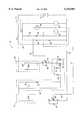
- the single drawing FIGUREdepicts the extended reverse battery protection circuit of this invention, as applied to an automotive cruise control circuit.
- the reference numeral 10generally designates an automotive cruise control circuit including a source voltage line 12 and a ground line 14.
- the ground line 14is electrically coupled to the negative terminal of a storage battery 16, and the source voltage line 12 is coupled to the positive terminal of battery 16 via an ignition key operated switch 18.
- the cruise control circuit 10includes an electric motor 20, an electromagnetic clutch 22 for selectively coupling the motor 20 to an engine throttle cable (not shown), and a micro-controller 24 for controlling the operation of the motor 20 and clutch 22.
- the clutch 22is electrically represented by the winding 22A
- the motor 20is represented by the winding 20A and the anti-parallel, or free-wheeling, diode 20B.
- the clutch winding 22Ais coupled to ground line 14 via the drain (D) and source (S) terminals of N-channel FET 26, which includes an intrinsic or body diode 28, and the gate (G) of FET 26 is connected to the micro-controller 24 via resistor 30.
- the motor winding 20Ais coupled to the drain (D) of N-channel FET 34, which includes an intrinsic or body diode 36, and the gate (G) of FET 34 is connected to the micro-controller 24 via resistor 38.
- the source (S) of FET 34is coupled to ground line 14 via the source (S) and drain (D) terminals of reverse voltage protection N-channel FET 40.
- motor 20may include one or more additional windings, as in the case of a stepper motor or a multi-phase brushless DC motor; in such case, the additional winding(s) and its control FET will be coupled between source voltage line 12 and the source (S) of reverse voltage protection FET 40--that is, in parallel with the series combination of winding 20A and FET 34.
- the micro-controller 24controls the FETs 26 and 34 to continuously energize the clutch winding 22A, and to pulse width modulate the motor winding 20A to produce a desired movement of the throttle cable (not shown).
- the micro-controller 24is depicted as a voltage source model, including a DC source 42 for establishing a regulated internal voltage reference VCC, a DC source 44 coupled to the resistor 30 for biasing FET 26 to a conductive state, and a square-wave voltage source 46 connected to the resistor 38 for biasing the FET 34 on and off, assuming that reverse voltage protection FET 40 is conductive.
- the source 44is referenced to ground and VCC by the intrinsic diodes 48 and 50, respectively, and the source 46 is referenced to ground and VCC by intrinsic diodes 52 and 54, respectively.
- the reverse voltage protection FET 40is the primary component of the extended reverse voltage protection circuit of this invention, designated by the reference numeral 60.
- the FET 40is connected in an inverse orientation, relative to the FET 34, and includes an intrinsic or body diode 62 as shown.
- a zener diode 64is connected across the gate-to-source circuit of the FET 40, and a capacitor 66 is connected in parallel with the diode 64.
- the gate (G) of FET 40is connected to the source voltage line 12 via the series combination of resistor 68 and diode 70, which form a charging circuit for the capacitor 66, and also via resistor 72, which forms a reverse transient discharge circuit for capacitor 66.
- the FET 40provides reverse battery protection for FET 34 by electrically isolating the source of FET 34 from ground line 14 when the positive and negative terminals of battery 16 are reversed, relative to the cruise control circuit 10. In that situation, the FET 40 is biased non-conductive since its gate and source terminals are at substantially the same potential, and the intrinsic diode 62 is reverse biased to block current which would otherwise flow in a low impedance path through diodes 36 and 20B.
- the capacitor 66quickly charges through the series combination of resistor 68 and diode 70. This raises the gate (G) of FET 40 to a higher potential than its source (S), biasing FET 40 to a conductive state, and electrically coupling ground line 14 to the source (S) of FET 34.
- the zener diode 64has a breakdown voltage of less than the rated gate-to-source voltage, so that it conducts to protect FET 40 in the event of excessive gate-to-source voltage.
- the charged capacitor 66 of protection circuit 60maintains the FET 40 in a conductive state for a predetermined interval after the source voltage interruption. During such interval, the source (S) terminal of FET 34 remains referenced to ground line 14, eliminating the possibility of a destructive gate-to-source voltage.
- the duration of the intervalis determined by the magnitude of the negative transient, and the time constant of capacitor 66 and resistor 72 through which capacitor 66 discharges during the transient.
- the extended reverse voltage protection circuit of the present inventionprovides protection from reverse voltage damage, whether due to reversed battery connections, or source voltage interruptions.
- reverse voltage damagewhether due to reversed battery connections, or source voltage interruptions.
- the inventionis not limited to use with cruise control circuits, or even automotive circuits in general. Accordingly, protection circuits incorporating these and other modifications may fall within the scope of this invention, which is defined by the appended claims.
Landscapes
- Charge And Discharge Circuits For Batteries Or The Like (AREA)
Abstract
Description
This invention relates to circuitry for protecting load circuit electronic devices from damage due to a source voltage polarity reversal, including transient voltages due to an interruption of the source voltage.
A common design requirement in automotive electronic applications is the provision of circuitry to protect electronic devices from damage due to reverse voltages. Most commonly, reverse voltages occur when the source (battery) cables are mistakenly reversed, or when improperly attempting to jump-start a disabled vehicle. A more intense, but limited duration situation occurs when the source voltage is suddenly interrupted, as may occur due to a loose or severed cable or connector; in such a case, interrupted reactive loads can produce relatively high reverse voltage transients that quickly damage electronic switching devices such as power transistors.
The need exists, therefore, to provide protection from reverse voltage damage, whether due to reversed battery connections, or source voltage interruptions.
The present invention is directed to an improved reverse voltage protection circuit that protects load circuit electronic devices from damage due to both reversed battery connections and source voltage interruptions.
According to the invention, a reverse voltage sensitive device is protected by a protection transistor connected between the negative terminal of the load circuit and ground, and the conduction of the protection transistor is extended during a reverse transient protection period following interruption of the source voltage. A capacitor connected to a control terminal of the protection transistor is charged from the source voltage through a low impedance charging circuit including a diode to prevent the capacitor from discharging, and is discharged during an interruption of the source voltage through a high impedance discharging circuit connected in parallel with the charging circuit.
If the battery connections are reversed with the capacitor discharged, the protection transistor will be non-conductive and an intrinsic diode across the current carrying terminals of the protection transistor will block current flow through the load circuit. When the battery connection is correctly established, the capacitor quickly charges through the low impedance charging path to bias the protection transistor conductive. The impedance of the discharge path is selected so that if the battery connection is subsequently interrupted, the capacitor will maintain the protection transistor in a conductive state to maintain the ground reference of the load circuit for a reverse protection interval which exceeds the expected duration of the resulting reverse voltage transient, thereby preventing damage to the load circuit electronic devices.
The single drawing FIGURE depicts the extended reverse battery protection circuit of this invention, as applied to an automotive cruise control circuit.
Referring to drawing, thereference numeral 10 generally designates an automotive cruise control circuit including asource voltage line 12 and aground line 14. Theground line 14 is electrically coupled to the negative terminal of a storage battery 16, and thesource voltage line 12 is coupled to the positive terminal of battery 16 via an ignition key operatedswitch 18. Thecruise control circuit 10 includes anelectric motor 20, an electromagnetic clutch 22 for selectively coupling themotor 20 to an engine throttle cable (not shown), and a micro-controller 24 for controlling the operation of themotor 20 and clutch 22. The clutch 22 is electrically represented by the winding 22A, and themotor 20 is represented by the winding 20A and the anti-parallel, or free-wheeling,diode 20B. Theclutch winding 22A is coupled toground line 14 via the drain (D) and source (S) terminals of N-channel FET 26, which includes an intrinsic or body diode 28, and the gate (G) of FET 26 is connected to the micro-controller 24 viaresistor 30. Themotor winding 20A is coupled to the drain (D) of N-channel FET 34, which includes an intrinsic orbody diode 36, and the gate (G) of FET 34 is connected to the micro-controller 24 viaresistor 38. The source (S) of FET 34 is coupled toground line 14 via the source (S) and drain (D) terminals of reverse voltage protection N-channel FET 40. Of course,motor 20 may include one or more additional windings, as in the case of a stepper motor or a multi-phase brushless DC motor; in such case, the additional winding(s) and its control FET will be coupled betweensource voltage line 12 and the source (S) of reverse voltage protection FET 40--that is, in parallel with the series combination of winding 20A and FET 34.
During cruise control operation, the micro-controller 24 controls theFETs 26 and 34 to continuously energize the clutch winding 22A, and to pulse width modulate the motor winding 20A to produce a desired movement of the throttle cable (not shown). The micro-controller 24 is depicted as a voltage source model, including a DC source 42 for establishing a regulated internal voltage reference VCC, a DC source 44 coupled to theresistor 30 for biasingFET 26 to a conductive state, and a square-wave voltage source 46 connected to theresistor 38 for biasing the FET 34 on and off, assuming that reverse voltage protection FET 40 is conductive. The source 44 is referenced to ground and VCC by theintrinsic diodes
The reverse voltage protection FET 40 is the primary component of the extended reverse voltage protection circuit of this invention, designated by thereference numeral 60. The FET 40 is connected in an inverse orientation, relative to the FET 34, and includes an intrinsic orbody diode 62 as shown. Azener diode 64 is connected across the gate-to-source circuit of the FET 40, and acapacitor 66 is connected in parallel with thediode 64. The gate (G) of FET 40 is connected to thesource voltage line 12 via the series combination ofresistor 68 and diode 70, which form a charging circuit for thecapacitor 66, and also via resistor 72, which forms a reverse transient discharge circuit forcapacitor 66.
The FET 40 provides reverse battery protection for FET 34 by electrically isolating the source of FET 34 fromground line 14 when the positive and negative terminals of battery 16 are reversed, relative to thecruise control circuit 10. In that situation, the FET 40 is biased non-conductive since its gate and source terminals are at substantially the same potential, and theintrinsic diode 62 is reverse biased to block current which would otherwise flow in a low impedance path throughdiodes
When the terminals of battery 16 are correctly connected to thecruise control circuit 10, thecapacitor 66 quickly charges through the series combination ofresistor 68 and diode 70. This raises the gate (G) of FET 40 to a higher potential than its source (S), biasing FET 40 to a conductive state, and electricallycoupling ground line 14 to the source (S) of FET 34. Thezener diode 64 has a breakdown voltage of less than the rated gate-to-source voltage, so that it conducts to protect FET 40 in the event of excessive gate-to-source voltage.
If the positive terminal of battery 16 is suddenly disconnected from the cruise control circuit 10 (as represented byopening ignition switch 18, for example), the supply of current toclutch coil 22A is suddenly interrupted. When this happens, a large negative transient voltage appears onvoltage source line 12. The negative transient forward biases theintrinsic diode 36 of FET 34, and if FET 40 were non-conductive, a large negative transient voltage would appear at the source (S) terminal of FET 34. Such a transient could easily damage the FET 34 since its gate (G) terminal remains substantially at ground potential due to the action ofintrinsic diode 48. That is, the resulting gate-to-source voltage Vgs could easily exceed the FET rating, possibly permanently damaging the FET 34. However, thecharged capacitor 66 ofprotection circuit 60 maintains the FET 40 in a conductive state for a predetermined interval after the source voltage interruption. During such interval, the source (S) terminal of FET 34 remains referenced toground line 14, eliminating the possibility of a destructive gate-to-source voltage. The duration of the interval is determined by the magnitude of the negative transient, and the time constant ofcapacitor 66 and resistor 72 through whichcapacitor 66 discharges during the transient. In a mechanization of the present invention, the resistor and capacitor values were as follows:capacitor 66=0.1 uF,resistor 68=10 kohm, and resistor 72=100 kohm. This provides a charging time constant of 1 msec, and a discharge time constant of 10 msec. Of course, other values could be used to achieve a similar result, and the time constants may vary from application to application.
In summary, the extended reverse voltage protection circuit of the present invention provides protection from reverse voltage damage, whether due to reversed battery connections, or source voltage interruptions. Although described in reference to the illustrated embodiment, it will be appreciated that various modifications will occur to those skilled in the art. For example, the invention is not limited to use with cruise control circuits, or even automotive circuits in general. Accordingly, protection circuits incorporating these and other modifications may fall within the scope of this invention, which is defined by the appended claims.
Claims (8)
1. A protected load circuit powered by a power source having first and second polarity terminals, comprising:
first and second load circuit terminals normally connected to the first and second terminals of said power source, respectively;
a load circuit including an electrical load, a load switching device, and a protection transistor connected in series, the electrical load being electrically coupled to the first load circuit terminal, and the protection transistor being electrically coupled to the second load circuit terminal, the protection transistor being effective in a conductive state to electrically couple said load switching device to the second load circuit terminal, and in a non-conductive state to electrically isolate the load switching device from the second load circuit terminal;
a capacitor coupled to a control terminal of said protection transistor, said capacitor being effective when charged to bias said protection transistor to said conductive state, and when discharged to bias said protection transistor to said non-conductive state;
a charging circuit for charging said capacitor to bias said protection transistor to said conductive state when the first and second load circuit terminals are connected to the first and second polarity terminal of said power source, respectively, but for allowing said capacitor to bias said protection transistor to said non-conductive state when the first and second polarity terminals of said power source are reversed; and
a discharging circuit for discharging said capacitor during a discharge interval when the voltage across said load circuit is momentarily reversed due to a disconnection of said power source, thereby allowing said protection transistor to remain in said conductive state during said discharge interval for protecting said load switching device from damage due to the momentary voltage reversal.
2. The protected load circuit of claim 1, wherein said protection transistor is a FET having a source terminal connected to said load switching device and said capacitor is connected between said control terminal and said source terminal.
3. The protected load circuit of claim 2, wherein said charging circuit comprises a first resistor and diode connected in series between said first load circuit terminal and said control terminal.
4. The protected load circuit of claim 3, wherein said discharging circuit comprises a second resistor connected in parallel with said charging circuit.
5. The protected load circuit of claim 2, wherein said discharging circuit includes a resistor connected between said first load circuit terminal and said control terminal.
6. The protected load circuit of claim 1, wherein said discharge interval is at least as long in duration as an expected duration of said momentary voltage reversal.
7. The protected load circuit of claim 1, wherein:
said protection transistor is a FET having a source terminal connected to said load switching device and said capacitor is connected between said control terminal and said source terminal;
said charging circuit comprises a first resistor and diode connected in series between said first load circuit terminal and said control terminal;
said discharging circuit comprises a second resistor connected in parallel with said charging circuit; and
said discharge interval is at least as long in duration as an expected duration of said momentary voltage reversal.
8. The protected load circuit of claim 7, wherein said load switching device is a FET having a source terminal connected to said protection transistor and a gate terminal referenced to said second load circuit terminal, the protection transistor operating during said discharge interval to maintain said source terminal at substantially the same potential as said gate terminal, thereby protecting said FET by limiting a potential difference between said gate and source terminals during said discharge interval.
Priority Applications (1)
| Application Number | Priority Date | Filing Date | Title |
|---|---|---|---|
| US09/333,461US6154081A (en) | 1999-06-15 | 1999-06-15 | Load circuit having extended reverse voltage protection |
Applications Claiming Priority (1)
| Application Number | Priority Date | Filing Date | Title |
|---|---|---|---|
| US09/333,461US6154081A (en) | 1999-06-15 | 1999-06-15 | Load circuit having extended reverse voltage protection |
Publications (1)
| Publication Number | Publication Date |
|---|---|
| US6154081Atrue US6154081A (en) | 2000-11-28 |
Family
ID=23302901
Family Applications (1)
| Application Number | Title | Priority Date | Filing Date |
|---|---|---|---|
| US09/333,461Expired - LifetimeUS6154081A (en) | 1999-06-15 | 1999-06-15 | Load circuit having extended reverse voltage protection |
Country Status (1)
| Country | Link |
|---|---|
| US (1) | US6154081A (en) |
Cited By (76)
| Publication number | Priority date | Publication date | Assignee | Title |
|---|---|---|---|---|
| US20030164694A1 (en)* | 2000-06-28 | 2003-09-04 | Josef Moseneder | Electronic circuit for an energy supply device, especially for a charging device for batteries |
| US6627555B2 (en)* | 1999-06-18 | 2003-09-30 | Saifun Semiconductors Ltd. | Method and circuit for minimizing the charging effect during manufacture of semiconductor devices |
| US6653820B1 (en) | 2002-01-30 | 2003-11-25 | National Semiconductor Corporation | Apparatus and method for protecting a battery cell from overcharging |
| US6670791B1 (en) | 2002-02-08 | 2003-12-30 | National Semiconductor Corporation | Dual path break before make digital circuit |
| US6724593B1 (en) | 2002-01-30 | 2004-04-20 | National Semiconductor Corporation | Reverse charger protection |
| US20040145353A1 (en)* | 2002-12-05 | 2004-07-29 | International Rectifier Corporation | Reverse battery protection circuit |
| US20040150927A1 (en)* | 2003-01-31 | 2004-08-05 | Strayer Lance R. | High side reverse and overvoltage transient protection |
| US20040151032A1 (en)* | 2003-01-30 | 2004-08-05 | Yan Polansky | High speed and low noise output buffer |
| US20040150929A1 (en)* | 2003-01-31 | 2004-08-05 | Strayer Lance R. | Overvoltage transient protection for low side circuits |
| US20040160712A1 (en)* | 2003-02-14 | 2004-08-19 | Zack Gary E. | Class II bus negative transient protection |
| US20040195870A1 (en)* | 2003-04-02 | 2004-10-07 | Catem Gmbh & Co. Kg; | Automotive vehicle seat and blower module for such an automotive vehicle seat |
| US20040233771A1 (en)* | 2001-10-24 | 2004-11-25 | Shor Joseph S. | Stack element circuit |
| US20050017688A1 (en)* | 2003-07-16 | 2005-01-27 | Dialog Semiconductor Gmbh | Protection switch with reverse voltage protection |
| US6885244B2 (en) | 2003-03-24 | 2005-04-26 | Saifun Semiconductors Ltd. | Operational amplifier with fast rise time |
| US20050122757A1 (en)* | 2003-12-03 | 2005-06-09 | Moore John T. | Memory architecture and method of manufacture and operation thereof |
| US6906966B2 (en) | 2003-06-16 | 2005-06-14 | Saifun Semiconductors Ltd. | Fast discharge for program and verification |
| US6919704B1 (en)* | 2003-07-09 | 2005-07-19 | Brunswick Corporation | Reverse battery protection for a trolling motor |
| US20050174152A1 (en)* | 2004-02-10 | 2005-08-11 | Alexander Kushnarenko | High voltage low power driver |
| US20050196737A1 (en)* | 2004-01-26 | 2005-09-08 | Mann Ralph V. | Systems and methods of measuring and evaluating performance of a physical skill and equipment used to perform the physical skill |
| US20050269619A1 (en)* | 2004-06-08 | 2005-12-08 | Shor Joseph S | MOS capacitor with reduced parasitic capacitance |
| US20050270089A1 (en)* | 2004-06-08 | 2005-12-08 | Shor Joseph S | Power-up and BGREF circuitry |
| US20060023381A1 (en)* | 2004-07-30 | 2006-02-02 | Taylor John P | System and method for protecting a load from a voltage source |
| US20060039219A1 (en)* | 2004-06-08 | 2006-02-23 | Yair Sofer | Replenishment for internal voltage |
| US20060152877A1 (en)* | 2005-01-12 | 2006-07-13 | Buzzard Brian W | Transient suppression circuit |
| US7095655B2 (en) | 2004-08-12 | 2006-08-22 | Saifun Semiconductors Ltd. | Dynamic matching of signal path and reference path for sensing |
| US20060202746A1 (en)* | 2005-03-10 | 2006-09-14 | Keming Chen | NMOS reverse battery protection |
| US7116577B2 (en) | 1997-08-01 | 2006-10-03 | Saifun Semiconductors Ltd | Two bit non-volatile electrically erasable and programmable semiconductor memory cell utilizing asymmetrical charge trapping |
| US7184313B2 (en) | 2005-06-17 | 2007-02-27 | Saifun Semiconductors Ltd. | Method circuit and system for compensating for temperature induced margin loss in non-volatile memory cells |
| US7221138B2 (en) | 2005-09-27 | 2007-05-22 | Saifun Semiconductors Ltd | Method and apparatus for measuring charge pump output current |
| US20070268048A1 (en)* | 2006-05-22 | 2007-11-22 | Fujitsu Ten Limited | Power supply control circuit, and electronic control device, power supplying circuit, and power control integrated circuit equipped with power supply control circuit |
| US7317633B2 (en) | 2004-07-06 | 2008-01-08 | Saifun Semiconductors Ltd | Protection of NROM devices from charge damage |
| US20080074064A1 (en)* | 2006-09-21 | 2008-03-27 | Danfoss Compressors Gmbh | Electric circuit providing protection from transients |
| US7352627B2 (en) | 2006-01-03 | 2008-04-01 | Saifon Semiconductors Ltd. | Method, system, and circuit for operating a non-volatile memory array |
| US7369440B2 (en) | 2005-01-19 | 2008-05-06 | Saifun Semiconductors Ltd. | Method, circuit and systems for erasing one or more non-volatile memory cells |
| US7420848B2 (en) | 2002-01-31 | 2008-09-02 | Saifun Semiconductors Ltd. | Method, system, and circuit for operating a non-volatile memory array |
| US7457183B2 (en) | 2003-09-16 | 2008-11-25 | Saifun Semiconductors Ltd. | Operating array cells with matched reference cells |
| US7512009B2 (en) | 2001-04-05 | 2009-03-31 | Saifun Semiconductors Ltd. | Method for programming a reference cell |
| US7518908B2 (en) | 2001-01-18 | 2009-04-14 | Saifun Semiconductors Ltd. | EEPROM array and method for operation thereof |
| US20090108911A1 (en)* | 2007-10-30 | 2009-04-30 | Rohm Co., Ltd. | Analog switch |
| US7532529B2 (en) | 2004-03-29 | 2009-05-12 | Saifun Semiconductors Ltd. | Apparatus and methods for multi-level sensing in a memory array |
| US7535765B2 (en) | 2004-12-09 | 2009-05-19 | Saifun Semiconductors Ltd. | Non-volatile memory device and method for reading cells |
| US7605579B2 (en) | 2006-09-18 | 2009-10-20 | Saifun Semiconductors Ltd. | Measuring and controlling current consumption and output current of charge pumps |
| US7638850B2 (en) | 2004-10-14 | 2009-12-29 | Saifun Semiconductors Ltd. | Non-volatile memory structure and method of fabrication |
| US7638835B2 (en) | 2006-02-28 | 2009-12-29 | Saifun Semiconductors Ltd. | Double density NROM with nitride strips (DDNS) |
| US7652930B2 (en) | 2004-04-01 | 2010-01-26 | Saifun Semiconductors Ltd. | Method, circuit and system for erasing one or more non-volatile memory cells |
| US7668017B2 (en) | 2005-08-17 | 2010-02-23 | Saifun Semiconductors Ltd. | Method of erasing non-volatile memory cells |
| US7675782B2 (en) | 2002-10-29 | 2010-03-09 | Saifun Semiconductors Ltd. | Method, system and circuit for programming a non-volatile memory array |
| US7692961B2 (en) | 2006-02-21 | 2010-04-06 | Saifun Semiconductors Ltd. | Method, circuit and device for disturb-control of programming nonvolatile memory cells by hot-hole injection (HHI) and by channel hot-electron (CHE) injection |
| US7701779B2 (en) | 2006-04-27 | 2010-04-20 | Sajfun Semiconductors Ltd. | Method for programming a reference cell |
| US7738304B2 (en) | 2002-07-10 | 2010-06-15 | Saifun Semiconductors Ltd. | Multiple use memory chip |
| US7743230B2 (en) | 2003-01-31 | 2010-06-22 | Saifun Semiconductors Ltd. | Memory array programming circuit and a method for using the circuit |
| US7760554B2 (en) | 2006-02-21 | 2010-07-20 | Saifun Semiconductors Ltd. | NROM non-volatile memory and mode of operation |
| US7786512B2 (en) | 2005-07-18 | 2010-08-31 | Saifun Semiconductors Ltd. | Dense non-volatile memory array and method of fabrication |
| US7808818B2 (en) | 2006-01-12 | 2010-10-05 | Saifun Semiconductors Ltd. | Secondary injection for NROM |
| US8053812B2 (en) | 2005-03-17 | 2011-11-08 | Spansion Israel Ltd | Contact in planar NROM technology |
| US8253452B2 (en) | 2006-02-21 | 2012-08-28 | Spansion Israel Ltd | Circuit and method for powering up an integrated circuit and an integrated circuit utilizing same |
| US8339102B2 (en) | 2004-02-10 | 2012-12-25 | Spansion Israel Ltd | System and method for regulating loading on an integrated circuit power supply |
| US8400841B2 (en) | 2005-06-15 | 2013-03-19 | Spansion Israel Ltd. | Device to program adjacent storage cells of different NROM cells |
| US8508898B2 (en) | 2012-01-11 | 2013-08-13 | Robert Bosch Gmbh | Diagnosable reverse-voltage protection for high power loads |
| US9008874B2 (en) | 2011-01-26 | 2015-04-14 | Toyota Motor Engineering & Manufacturing North America, Inc. | System and method for managing power in a vehicle |
| JP2015165745A (en)* | 2014-03-03 | 2015-09-17 | オムロンオートモーティブエレクトロニクス株式会社 | Power supply circuit |
| JP2015211163A (en)* | 2014-04-28 | 2015-11-24 | 株式会社東芝 | Semiconductor integrated circuit |
| US9219412B2 (en) | 2012-06-07 | 2015-12-22 | Nxp B.V. | Buck converter with reverse current protection, and a photovoltaic system |
| US20160285353A1 (en)* | 2015-03-27 | 2016-09-29 | Samsung Electronics Co., Ltd. | Switch driving circuit, and power factor correction circuit having the same |
| TWI556406B (en)* | 2010-02-19 | 2016-11-01 | 半導體能源研究所股份有限公司 | Semiconductor device |
| US9584119B2 (en) | 2013-04-23 | 2017-02-28 | Honeywell International Inc. | Triac or bypass circuit and MOSFET power steal combination |
| US9628074B2 (en) | 2014-06-19 | 2017-04-18 | Honeywell International Inc. | Bypass switch for in-line power steal |
| US9673811B2 (en) | 2013-11-22 | 2017-06-06 | Honeywell International Inc. | Low power consumption AC load switches |
| US9683749B2 (en) | 2014-07-11 | 2017-06-20 | Honeywell International Inc. | Multiple heatsink cooling system for a line voltage thermostat |
| US9806705B2 (en) | 2013-04-23 | 2017-10-31 | Honeywell International Inc. | Active triac triggering circuit |
| US9857091B2 (en) | 2013-11-22 | 2018-01-02 | Honeywell International Inc. | Thermostat circuitry to control power usage |
| US9983244B2 (en) | 2013-06-28 | 2018-05-29 | Honeywell International Inc. | Power transformation system with characterization |
| US10099560B2 (en) | 2011-01-26 | 2018-10-16 | Toyota Motor Engineering & Manufacturing North America, Inc. | System and method for maintaining the speed of a vehicle |
| US10139843B2 (en) | 2012-02-22 | 2018-11-27 | Honeywell International Inc. | Wireless thermostatic controlled electric heating system |
| US10811892B2 (en) | 2013-06-28 | 2020-10-20 | Ademco Inc. | Source management for a power transformation system |
| US11054448B2 (en) | 2013-06-28 | 2021-07-06 | Ademco Inc. | Power transformation self characterization mode |
Citations (2)
| Publication number | Priority date | Publication date | Assignee | Title |
|---|---|---|---|---|
| US4763235A (en)* | 1986-01-16 | 1988-08-09 | Sanken Electric Co., Ltd. | DC-DC converter |
| US5339210A (en)* | 1992-07-22 | 1994-08-16 | General Electric Company | DC circuit interrupter |
- 1999
- 1999-06-15USUS09/333,461patent/US6154081A/ennot_activeExpired - Lifetime
Patent Citations (2)
| Publication number | Priority date | Publication date | Assignee | Title |
|---|---|---|---|---|
| US4763235A (en)* | 1986-01-16 | 1988-08-09 | Sanken Electric Co., Ltd. | DC-DC converter |
| US5339210A (en)* | 1992-07-22 | 1994-08-16 | General Electric Company | DC circuit interrupter |
Cited By (101)
| Publication number | Priority date | Publication date | Assignee | Title |
|---|---|---|---|---|
| US7405969B2 (en) | 1997-08-01 | 2008-07-29 | Saifun Semiconductors Ltd. | Non-volatile memory cell and non-volatile memory devices |
| US7116577B2 (en) | 1997-08-01 | 2006-10-03 | Saifun Semiconductors Ltd | Two bit non-volatile electrically erasable and programmable semiconductor memory cell utilizing asymmetrical charge trapping |
| US6627555B2 (en)* | 1999-06-18 | 2003-09-30 | Saifun Semiconductors Ltd. | Method and circuit for minimizing the charging effect during manufacture of semiconductor devices |
| US6774607B2 (en)* | 2000-06-28 | 2004-08-10 | Fronius International Gmbh | Charger connected to a load via a switching circuit to prevent an incorrect polarity connection |
| US20030164694A1 (en)* | 2000-06-28 | 2003-09-04 | Josef Moseneder | Electronic circuit for an energy supply device, especially for a charging device for batteries |
| US7518908B2 (en) | 2001-01-18 | 2009-04-14 | Saifun Semiconductors Ltd. | EEPROM array and method for operation thereof |
| US7512009B2 (en) | 2001-04-05 | 2009-03-31 | Saifun Semiconductors Ltd. | Method for programming a reference cell |
| US20040233771A1 (en)* | 2001-10-24 | 2004-11-25 | Shor Joseph S. | Stack element circuit |
| US6724593B1 (en) | 2002-01-30 | 2004-04-20 | National Semiconductor Corporation | Reverse charger protection |
| US6653820B1 (en) | 2002-01-30 | 2003-11-25 | National Semiconductor Corporation | Apparatus and method for protecting a battery cell from overcharging |
| US7420848B2 (en) | 2002-01-31 | 2008-09-02 | Saifun Semiconductors Ltd. | Method, system, and circuit for operating a non-volatile memory array |
| US6670791B1 (en) | 2002-02-08 | 2003-12-30 | National Semiconductor Corporation | Dual path break before make digital circuit |
| US7738304B2 (en) | 2002-07-10 | 2010-06-15 | Saifun Semiconductors Ltd. | Multiple use memory chip |
| US7675782B2 (en) | 2002-10-29 | 2010-03-09 | Saifun Semiconductors Ltd. | Method, system and circuit for programming a non-volatile memory array |
| US20040145353A1 (en)* | 2002-12-05 | 2004-07-29 | International Rectifier Corporation | Reverse battery protection circuit |
| US6969971B2 (en)* | 2002-12-05 | 2005-11-29 | International Rectifier Corporation | Reverse battery protection circuit |
| US20040151032A1 (en)* | 2003-01-30 | 2004-08-05 | Yan Polansky | High speed and low noise output buffer |
| US6922322B2 (en) | 2003-01-31 | 2005-07-26 | Delphi Technologies, Inc. | High side reverse and overvoltage transient protection |
| US6975493B2 (en) | 2003-01-31 | 2005-12-13 | Delphi Technologies, Inc. | Overvoltage transient protection for low side circuits |
| US20040150927A1 (en)* | 2003-01-31 | 2004-08-05 | Strayer Lance R. | High side reverse and overvoltage transient protection |
| US20040150929A1 (en)* | 2003-01-31 | 2004-08-05 | Strayer Lance R. | Overvoltage transient protection for low side circuits |
| US7743230B2 (en) | 2003-01-31 | 2010-06-22 | Saifun Semiconductors Ltd. | Memory array programming circuit and a method for using the circuit |
| US20040160712A1 (en)* | 2003-02-14 | 2004-08-19 | Zack Gary E. | Class II bus negative transient protection |
| US7061734B2 (en) | 2003-02-14 | 2006-06-13 | Visteon Global Technologies, Inc. | Class II bus negative transient protection |
| US6885244B2 (en) | 2003-03-24 | 2005-04-26 | Saifun Semiconductors Ltd. | Operational amplifier with fast rise time |
| US20040195870A1 (en)* | 2003-04-02 | 2004-10-07 | Catem Gmbh & Co. Kg; | Automotive vehicle seat and blower module for such an automotive vehicle seat |
| US6906966B2 (en) | 2003-06-16 | 2005-06-14 | Saifun Semiconductors Ltd. | Fast discharge for program and verification |
| US6919704B1 (en)* | 2003-07-09 | 2005-07-19 | Brunswick Corporation | Reverse battery protection for a trolling motor |
| US7030591B2 (en) | 2003-07-16 | 2006-04-18 | Dialog Semiconductor Gmbh | Integrated circuit implementing protection switch for battery charging and discharging with enhanced reverse voltage protection |
| US20050017688A1 (en)* | 2003-07-16 | 2005-01-27 | Dialog Semiconductor Gmbh | Protection switch with reverse voltage protection |
| US7457183B2 (en) | 2003-09-16 | 2008-11-25 | Saifun Semiconductors Ltd. | Operating array cells with matched reference cells |
| US20050122757A1 (en)* | 2003-12-03 | 2005-06-09 | Moore John T. | Memory architecture and method of manufacture and operation thereof |
| US20050196737A1 (en)* | 2004-01-26 | 2005-09-08 | Mann Ralph V. | Systems and methods of measuring and evaluating performance of a physical skill and equipment used to perform the physical skill |
| US8339102B2 (en) | 2004-02-10 | 2012-12-25 | Spansion Israel Ltd | System and method for regulating loading on an integrated circuit power supply |
| US7176728B2 (en) | 2004-02-10 | 2007-02-13 | Saifun Semiconductors Ltd | High voltage low power driver |
| US20050174152A1 (en)* | 2004-02-10 | 2005-08-11 | Alexander Kushnarenko | High voltage low power driver |
| US7532529B2 (en) | 2004-03-29 | 2009-05-12 | Saifun Semiconductors Ltd. | Apparatus and methods for multi-level sensing in a memory array |
| US7652930B2 (en) | 2004-04-01 | 2010-01-26 | Saifun Semiconductors Ltd. | Method, circuit and system for erasing one or more non-volatile memory cells |
| US20050269619A1 (en)* | 2004-06-08 | 2005-12-08 | Shor Joseph S | MOS capacitor with reduced parasitic capacitance |
| US7190212B2 (en) | 2004-06-08 | 2007-03-13 | Saifun Semiconductors Ltd | Power-up and BGREF circuitry |
| US7256438B2 (en) | 2004-06-08 | 2007-08-14 | Saifun Semiconductors Ltd | MOS capacitor with reduced parasitic capacitance |
| US7187595B2 (en) | 2004-06-08 | 2007-03-06 | Saifun Semiconductors Ltd. | Replenishment for internal voltage |
| US20060039219A1 (en)* | 2004-06-08 | 2006-02-23 | Yair Sofer | Replenishment for internal voltage |
| US20050270089A1 (en)* | 2004-06-08 | 2005-12-08 | Shor Joseph S | Power-up and BGREF circuitry |
| US7317633B2 (en) | 2004-07-06 | 2008-01-08 | Saifun Semiconductors Ltd | Protection of NROM devices from charge damage |
| US7139157B2 (en) | 2004-07-30 | 2006-11-21 | Kyocera Wireless Corp. | System and method for protecting a load from a voltage source |
| US20060023381A1 (en)* | 2004-07-30 | 2006-02-02 | Taylor John P | System and method for protecting a load from a voltage source |
| US7466594B2 (en) | 2004-08-12 | 2008-12-16 | Saifun Semiconductors Ltd. | Dynamic matching of signal path and reference path for sensing |
| US7095655B2 (en) | 2004-08-12 | 2006-08-22 | Saifun Semiconductors Ltd. | Dynamic matching of signal path and reference path for sensing |
| US7964459B2 (en) | 2004-10-14 | 2011-06-21 | Spansion Israel Ltd. | Non-volatile memory structure and method of fabrication |
| US7638850B2 (en) | 2004-10-14 | 2009-12-29 | Saifun Semiconductors Ltd. | Non-volatile memory structure and method of fabrication |
| US7535765B2 (en) | 2004-12-09 | 2009-05-19 | Saifun Semiconductors Ltd. | Non-volatile memory device and method for reading cells |
| US20060152877A1 (en)* | 2005-01-12 | 2006-07-13 | Buzzard Brian W | Transient suppression circuit |
| WO2006076219A3 (en)* | 2005-01-12 | 2006-11-23 | American Prec Ind Inc | A transient suppression circuit |
| US7369440B2 (en) | 2005-01-19 | 2008-05-06 | Saifun Semiconductors Ltd. | Method, circuit and systems for erasing one or more non-volatile memory cells |
| US7468926B2 (en) | 2005-01-19 | 2008-12-23 | Saifun Semiconductors Ltd. | Partial erase verify |
| US7312653B2 (en)* | 2005-03-10 | 2007-12-25 | Gm Global Technology Operations, Inc. | NMOS reverse battery protection |
| US20060202746A1 (en)* | 2005-03-10 | 2006-09-14 | Keming Chen | NMOS reverse battery protection |
| US8053812B2 (en) | 2005-03-17 | 2011-11-08 | Spansion Israel Ltd | Contact in planar NROM technology |
| US8400841B2 (en) | 2005-06-15 | 2013-03-19 | Spansion Israel Ltd. | Device to program adjacent storage cells of different NROM cells |
| US7184313B2 (en) | 2005-06-17 | 2007-02-27 | Saifun Semiconductors Ltd. | Method circuit and system for compensating for temperature induced margin loss in non-volatile memory cells |
| US7786512B2 (en) | 2005-07-18 | 2010-08-31 | Saifun Semiconductors Ltd. | Dense non-volatile memory array and method of fabrication |
| US7668017B2 (en) | 2005-08-17 | 2010-02-23 | Saifun Semiconductors Ltd. | Method of erasing non-volatile memory cells |
| US7221138B2 (en) | 2005-09-27 | 2007-05-22 | Saifun Semiconductors Ltd | Method and apparatus for measuring charge pump output current |
| US7352627B2 (en) | 2006-01-03 | 2008-04-01 | Saifon Semiconductors Ltd. | Method, system, and circuit for operating a non-volatile memory array |
| US7808818B2 (en) | 2006-01-12 | 2010-10-05 | Saifun Semiconductors Ltd. | Secondary injection for NROM |
| US7692961B2 (en) | 2006-02-21 | 2010-04-06 | Saifun Semiconductors Ltd. | Method, circuit and device for disturb-control of programming nonvolatile memory cells by hot-hole injection (HHI) and by channel hot-electron (CHE) injection |
| US7760554B2 (en) | 2006-02-21 | 2010-07-20 | Saifun Semiconductors Ltd. | NROM non-volatile memory and mode of operation |
| US8253452B2 (en) | 2006-02-21 | 2012-08-28 | Spansion Israel Ltd | Circuit and method for powering up an integrated circuit and an integrated circuit utilizing same |
| US7638835B2 (en) | 2006-02-28 | 2009-12-29 | Saifun Semiconductors Ltd. | Double density NROM with nitride strips (DDNS) |
| US7701779B2 (en) | 2006-04-27 | 2010-04-20 | Sajfun Semiconductors Ltd. | Method for programming a reference cell |
| US20070268048A1 (en)* | 2006-05-22 | 2007-11-22 | Fujitsu Ten Limited | Power supply control circuit, and electronic control device, power supplying circuit, and power control integrated circuit equipped with power supply control circuit |
| US7800878B2 (en)* | 2006-05-22 | 2010-09-21 | Fujitsu Ten Limited | Power supply control circuit, and electronic control device, power supplying circuit, and power control integrated circuit equipped with power supply control circuit |
| US7605579B2 (en) | 2006-09-18 | 2009-10-20 | Saifun Semiconductors Ltd. | Measuring and controlling current consumption and output current of charge pumps |
| US8063597B2 (en) | 2006-09-21 | 2011-11-22 | Secop Gmbh | Electric circuit providing protection from transients |
| US20080074064A1 (en)* | 2006-09-21 | 2008-03-27 | Danfoss Compressors Gmbh | Electric circuit providing protection from transients |
| US8149042B2 (en) | 2007-10-30 | 2012-04-03 | Rohm Co., Ltd. | Analog switch for signal swinging between positive and negative voltages |
| US20090108911A1 (en)* | 2007-10-30 | 2009-04-30 | Rohm Co., Ltd. | Analog switch |
| TWI556406B (en)* | 2010-02-19 | 2016-11-01 | 半導體能源研究所股份有限公司 | Semiconductor device |
| US9008874B2 (en) | 2011-01-26 | 2015-04-14 | Toyota Motor Engineering & Manufacturing North America, Inc. | System and method for managing power in a vehicle |
| US10099560B2 (en) | 2011-01-26 | 2018-10-16 | Toyota Motor Engineering & Manufacturing North America, Inc. | System and method for maintaining the speed of a vehicle |
| US8508898B2 (en) | 2012-01-11 | 2013-08-13 | Robert Bosch Gmbh | Diagnosable reverse-voltage protection for high power loads |
| US10139843B2 (en) | 2012-02-22 | 2018-11-27 | Honeywell International Inc. | Wireless thermostatic controlled electric heating system |
| US9219412B2 (en) | 2012-06-07 | 2015-12-22 | Nxp B.V. | Buck converter with reverse current protection, and a photovoltaic system |
| US10404253B2 (en) | 2013-04-23 | 2019-09-03 | Ademco Inc. | Triac or bypass circuit and MOSFET power steal combination |
| US9584119B2 (en) | 2013-04-23 | 2017-02-28 | Honeywell International Inc. | Triac or bypass circuit and MOSFET power steal combination |
| US9806705B2 (en) | 2013-04-23 | 2017-10-31 | Honeywell International Inc. | Active triac triggering circuit |
| US10396770B2 (en) | 2013-04-23 | 2019-08-27 | Ademco Inc. | Active triac triggering circuit |
| US11054448B2 (en) | 2013-06-28 | 2021-07-06 | Ademco Inc. | Power transformation self characterization mode |
| US10811892B2 (en) | 2013-06-28 | 2020-10-20 | Ademco Inc. | Source management for a power transformation system |
| US9983244B2 (en) | 2013-06-28 | 2018-05-29 | Honeywell International Inc. | Power transformation system with characterization |
| US9673811B2 (en) | 2013-11-22 | 2017-06-06 | Honeywell International Inc. | Low power consumption AC load switches |
| US9857091B2 (en) | 2013-11-22 | 2018-01-02 | Honeywell International Inc. | Thermostat circuitry to control power usage |
| JP2015165745A (en)* | 2014-03-03 | 2015-09-17 | オムロンオートモーティブエレクトロニクス株式会社 | Power supply circuit |
| JP2015211163A (en)* | 2014-04-28 | 2015-11-24 | 株式会社東芝 | Semiconductor integrated circuit |
| US10353411B2 (en) | 2014-06-19 | 2019-07-16 | Ademco Inc. | Bypass switch for in-line power steal |
| US9628074B2 (en) | 2014-06-19 | 2017-04-18 | Honeywell International Inc. | Bypass switch for in-line power steal |
| US10088174B2 (en) | 2014-07-11 | 2018-10-02 | Honeywell International Inc. | Multiple heatsink cooling system for a line voltage thermostat |
| US9683749B2 (en) | 2014-07-11 | 2017-06-20 | Honeywell International Inc. | Multiple heatsink cooling system for a line voltage thermostat |
| US9762119B2 (en)* | 2015-03-27 | 2017-09-12 | Samsung Electronics Co., Ltd. | Switch driving circuit, and power factor correction circuit having the same |
| US20160285353A1 (en)* | 2015-03-27 | 2016-09-29 | Samsung Electronics Co., Ltd. | Switch driving circuit, and power factor correction circuit having the same |
Similar Documents
| Publication | Publication Date | Title |
|---|---|---|
| US6154081A (en) | Load circuit having extended reverse voltage protection | |
| US6353307B1 (en) | Controlled rectifier bridge with over-voltage protection | |
| US5539610A (en) | Floating drive technique for reverse battery protection | |
| EP0542365B1 (en) | Electric circuit comprising deep discharge protection for rechargeable batteries | |
| US6043965A (en) | Low loss reverse battery protection | |
| US20020109952A1 (en) | High voltage battery cutout circuit for a motor vehicle electrical system | |
| EP2363936B1 (en) | Reverse connection protecting device and backup power supply comprising the same | |
| US5914545A (en) | Switching device with power FET and short-circuit detection | |
| EP2071725B1 (en) | Power supply control circuit | |
| JP2003037933A (en) | Protection apparatus of electronic equipment | |
| US7288856B2 (en) | Reverse battery protection circuit for power switch | |
| US11228305B2 (en) | Load drive circuit configured to prevent a flyback current | |
| US6670724B2 (en) | Series pass over-voltage protection circuit for a motor vehicle electrical system | |
| US6738245B2 (en) | Series-pass over-voltage protection circuit having multiple transistors in parallel | |
| US7327546B2 (en) | Power switching circuit with active clamp disconnect for load dump protection | |
| US20030223170A1 (en) | High current series-pass over-voltage protection circuit | |
| KR20010041222A (en) | POWER SUPPLIES FOR ECUs | |
| US6369533B1 (en) | Piloting circuit for an inductive load in particular for a DC electric motor | |
| EP0341460B1 (en) | Driver protection circuit | |
| US5923095A (en) | Control apparatus for onboard AC generator for motor vehicle | |
| US6856495B2 (en) | Series pass over-voltage protection circuit having low quiescent current draw | |
| US20060232901A1 (en) | Arrangement for protecting an electrical device | |
| US6819535B2 (en) | Device for protecting loads supplied by an alternator | |
| CN111664043B (en) | Semiconductor integrated circuit having a plurality of transistors | |
| US6639444B2 (en) | Protection circuit |
Legal Events
| Date | Code | Title | Description |
|---|---|---|---|
| STCF | Information on status: patent grant | Free format text:PATENTED CASE | |
| AS | Assignment | Owner name:DELPHI TECHNOLOGIES, INC., MICHIGAN Free format text:ASSIGNMENT OF ASSIGNORS INTEREST;ASSIGNORS:PARKKALA, WILLIAM FRANK;KEKEL, STEVEN C.;DU BOIS, PAUL LOUIS;AND OTHERS;REEL/FRAME:011699/0701;SIGNING DATES FROM 20001201 TO 20001212 | |
| FPAY | Fee payment | Year of fee payment:4 | |
| FPAY | Fee payment | Year of fee payment:8 | |
| FPAY | Fee payment | Year of fee payment:12 | |
| AS | Assignment | Owner name:DELPHI TECHNOLOGIES IP LIMITED, BARBADOS Free format text:ASSIGNMENT OF ASSIGNORS INTEREST;ASSIGNOR:DELPHI TECHNOLOGIES, INC.;REEL/FRAME:045102/0409 Effective date:20171129 |