US6154073A - Delay locked loop device of the semiconductor circuit - Google Patents
Delay locked loop device of the semiconductor circuitDownload PDFInfo
- Publication number
- US6154073A US6154073AUS09/196,121US19612198AUS6154073AUS 6154073 AUS6154073 AUS 6154073AUS 19612198 AUS19612198 AUS 19612198AUS 6154073 AUS6154073 AUS 6154073A
- Authority
- US
- United States
- Prior art keywords
- delay
- phase
- internal clock
- clock
- delay means
- Prior art date
- Legal status (The legal status is an assumption and is not a legal conclusion. Google has not performed a legal analysis and makes no representation as to the accuracy of the status listed.)
- Expired - Lifetime
Links
Images
Classifications
- G—PHYSICS
- G11—INFORMATION STORAGE
- G11C—STATIC STORES
- G11C11/00—Digital stores characterised by the use of particular electric or magnetic storage elements; Storage elements therefor
- G11C11/21—Digital stores characterised by the use of particular electric or magnetic storage elements; Storage elements therefor using electric elements
- G11C11/34—Digital stores characterised by the use of particular electric or magnetic storage elements; Storage elements therefor using electric elements using semiconductor devices
- G11C11/40—Digital stores characterised by the use of particular electric or magnetic storage elements; Storage elements therefor using electric elements using semiconductor devices using transistors
- G11C11/401—Digital stores characterised by the use of particular electric or magnetic storage elements; Storage elements therefor using electric elements using semiconductor devices using transistors forming cells needing refreshing or charge regeneration, i.e. dynamic cells
- G11C11/4063—Auxiliary circuits, e.g. for addressing, decoding, driving, writing, sensing or timing
- G11C11/407—Auxiliary circuits, e.g. for addressing, decoding, driving, writing, sensing or timing for memory cells of the field-effect type
- H—ELECTRICITY
- H03—ELECTRONIC CIRCUITRY
- H03L—AUTOMATIC CONTROL, STARTING, SYNCHRONISATION OR STABILISATION OF GENERATORS OF ELECTRONIC OSCILLATIONS OR PULSES
- H03L7/00—Automatic control of frequency or phase; Synchronisation
- H03L7/06—Automatic control of frequency or phase; Synchronisation using a reference signal applied to a frequency- or phase-locked loop
- H03L7/08—Details of the phase-locked loop
- H03L7/081—Details of the phase-locked loop provided with an additional controlled phase shifter
- H03L7/0812—Details of the phase-locked loop provided with an additional controlled phase shifter and where no voltage or current controlled oscillator is used
- H03L7/0814—Details of the phase-locked loop provided with an additional controlled phase shifter and where no voltage or current controlled oscillator is used the phase shifting device being digitally controlled
- H—ELECTRICITY
- H03—ELECTRONIC CIRCUITRY
- H03L—AUTOMATIC CONTROL, STARTING, SYNCHRONISATION OR STABILISATION OF GENERATORS OF ELECTRONIC OSCILLATIONS OR PULSES
- H03L7/00—Automatic control of frequency or phase; Synchronisation
- H03L7/06—Automatic control of frequency or phase; Synchronisation using a reference signal applied to a frequency- or phase-locked loop
- H03L7/08—Details of the phase-locked loop
- H03L7/081—Details of the phase-locked loop provided with an additional controlled phase shifter
- H03L7/0812—Details of the phase-locked loop provided with an additional controlled phase shifter and where no voltage or current controlled oscillator is used
- H03L7/0816—Details of the phase-locked loop provided with an additional controlled phase shifter and where no voltage or current controlled oscillator is used the controlled phase shifter and the frequency- or phase-detection arrangement being connected to a common input
- H—ELECTRICITY
- H03—ELECTRONIC CIRCUITRY
- H03L—AUTOMATIC CONTROL, STARTING, SYNCHRONISATION OR STABILISATION OF GENERATORS OF ELECTRONIC OSCILLATIONS OR PULSES
- H03L7/00—Automatic control of frequency or phase; Synchronisation
- H03L7/06—Automatic control of frequency or phase; Synchronisation using a reference signal applied to a frequency- or phase-locked loop
- H03L7/08—Details of the phase-locked loop
- H03L7/085—Details of the phase-locked loop concerning mainly the frequency- or phase-detection arrangement including the filtering or amplification of its output signal
- H03L7/089—Details of the phase-locked loop concerning mainly the frequency- or phase-detection arrangement including the filtering or amplification of its output signal the phase or frequency detector generating up-down pulses
- H03L7/0891—Details of the phase-locked loop concerning mainly the frequency- or phase-detection arrangement including the filtering or amplification of its output signal the phase or frequency detector generating up-down pulses the up-down pulses controlling source and sink current generators, e.g. a charge pump
Definitions
- the present inventionrelates to a clock compensation device of the semiconductor circuit, and more particularly, to a Delay Locked Loop device which is type of the clock compensation devices generating an internal clock by receiving an external clock.
- Delay Locked Loop devicegenerates an internal clock by receiving an external clock. It is utilized to match the frequency and the phase of the external clock and the internal clock.
- Delay Locked Loop deviceincludes a phase detector, a charge pump and a delay means.
- the phase detectorcompares and detects the difference of frequency or the difference of the phase of the external clock and the internal clock.
- the charge pumpwhich receives the output signal from the phase detector and outputs the pumping signal controls the delay time of the delay means by controlling delay elements in the delay means.
- the delay meansis controlled by the output signal from the charge pump and outputs the internal clock by receiving the output clock.
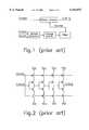
- FIG. 1is a block diagram of a Delay Locked Loop device of a prior art.
- Delay Locked Loop device in FIG. 1further includes a filter to eliminate noises in the output signal from the charge pump.
- FIG. 2is a detailed circuit of a delay means in FIG. 1.
- the delay meansincludes a plurality of delay elements. As described above, the delay means generates an internal clock by receiving an external clock. The phase difference and the frequency difference between the internal and external clock are controlled by the pump voltage Vpump from the charge pump.
- the delay meanswhen an external clock is inputted, the delay means generates a certain internal clock when the pump voltage Vpump maintains an arbitrary voltage level.
- the phase detectorcompares and detects the frequency and/or phase of the external and internal clock.
- charge pumpmaintains the initial pump voltage Vpump and the phase detector outputs no signal.
- the phase detectorgenerates an output signal to control charge pump. Then, the charge pump outputs a controlled pump voltage Vpump.
- the voltage level of the controlled pump voltage Vpumpincreases or decreases in accordance with the state of the output signal from the phase detector.
- the phase detectoroutputs high voltage level to raise the level of the pump voltage Vpump from the charge pump to compensate the lag in the internal clock.
- the increase in pump voltage Vpumpis inputted to the bias transistors of the delay elements, which consist of CMOS transistors, to shorten the delay time. Accordingly, the lag phase of the internal clock is compensated. If the phase of the internal clock is faster, then the phase detector compares the difference of two phases and outputs low voltage level to decrease the level of the pump voltage Vpump from the charge pump to compensate the faster phase of the internal clock.
- the Delay Locked Loop devicearrives at the Lock state.
- Lock stateindicates that the frequencies and/or phases of the external clock and internal clock match.
- the Delay Locked Loop devicecontrols the delay time by controlling the bias transistors in the delay elements.
- the pump voltage levelchanges slowly because the output signal from the charge pump is an analog signal.
- the delay time of the Delay Locked Loop devicealso changes slowly. Accordingly, very long Lock time is required in order to match frequencies and/or phases between the external clock and internal clock.
- the frequency bandwidth of the Delay Locked Loop device in a prior artis confined to certain range because the entire delay time of the delay means is fixed.
- Another object of the inventionis to provide a Delay Locked Loop device which includes a plurality of the delay elements each of which outputs different delay times.
- another object of the inventionis to provide a Delay Locked Loop device which includes a phase detector for detecting the phase difference, and includes counter for selecting one of the output signals from the delay elements.
- the present inventionis directed to a Delay Locked Loop device which is one of the clock compensation devices generating an internal clock by receiving an external clock.
- Delay Locked Loop devicethat is one embodiment of the present invention comprises, delay means for receiving an external clock and generating an internal clock, said delay means having a first to Nth delay elements delaying the received external clock in order to match the phase of the external clock with the phase of the internal clock; phase detector for outputting detect signal which discriminates differences between the phase of the external clock and the phase of the external clock; counter for receiving the detect signal from the phase detector, outputting a first control signal to control the phase of the internal clock generated from the delay means, and outputting a second control signal to contol the delay range of the delay means when the difference between the phase of the external clock and the phase of the internal clock exceeds the delay range of the delay means; and charge pump for receiving the second control signal outputted from the counter, and generating pump voltage which controls the delay means in order to make the difference between the phase of the external clock and phase of the internal clock exist within the delay range of the first to Nth delay means.
- the frequency of the external clockis identical with the frequency of the internal clock.
- the internal clock outputted from the delay meansis an output signal from one of the first to Nth delay elements selected by the first control signal generated from the counter.
- the embodiment of the inventionfurther comprises a filter for outputting noiseless pump voltage by receiving the pump voltage from the charge pump.
- the delay means of the inventioncomprises a multiplexer for receiving N delay signals outputted from each of the first to Nth delay elements and outputting one of the N delay signals as the internal clock in accordance with the first control signal from the counter.
- FIG. 1is a block diagram of a Delay Locked Loop device of a prior art
- FIG. 2is a detailed circuit of the delay means in prior art
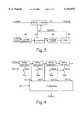
- FIG. 3is a block diagram of a Delay Locked Loop device of the present invention.
- FIG. 4is a detailed circuit of the delay means in the present invention.
- FIG. 3is a block diagram of a Delay Locked Loop device of the present invention.
- Delay means 10receives a external clock CLKext and generates an internal clock CLKint.
- Delay meanshave a first to Nth delay elements for delaying the received external clock in order to match the phase of the external clock with the phase of the internal clock. It will be explained hereinafter with reference to FIG. 4.
- Phase detector 20outputs detecting signal which discriminates the phase difference between the phase of the internal clock and phase of the external clock.
- Counter 30receives the detecting signal from the phase detector and outputs a first control signal Qi to control the phase of the internal clock generated from the delay means, and outputs a second control signal Pi to control the delay range of the delay means when the difference between the phase of the external clock and phase of the internal clock exceeds the delay range of the delay means.
- Charge pump 40receives the second control signal Pi outputted from the counter and generates pump voltage Vpump that controls the delay means which makes the difference between the phase of the external clock and the phase of the internal clock exist within the delay range of the first to Nth delay means.
- the frequency of the external clockis identical with the frequency of the internal clock.
- the internal clock generated from the delay meansis one of the output signals from the first to Nth delay elements by the control of the first control signal from the counter.
- the Delay Locked Loop devicefurther comprises a filter 50 for receiving the pump voltage outputted from the charge pump and generating a noiseless pump voltage by eliminating the noise in the pump voltage.
- FIG. 4is a detailed circuit of the delay means in FIG. 3.
- delay meansincludes a plurality of delay elements 11, 12, 13 and 14 which generate internal clocks OUT0, OUT1, OUT3 and OUT4 (each of the delay times of the internal clocks is different); a plurality of N-type MOS transistors MN1, MN2, MN3 and MN4 which are controlled by the pump voltage Vpump inputted to each gate of the transistors to control the delay time of the delay elements; and multiplexer 15 for receiving a plurality of the internal clocks OUT0, OUT1, OUT3 and OUT4 and selecting one of the internal clocks OUT0, OUT1, OUT3 and OUT4 in response to the control signal outputted from the counter.
- pump voltage Vpump outputted from the charge pump 40maintains an arbitrary voltage level. Sizes of the transistors constituting the delay elements also is determined when it is designed. For example, if the delay time is determined as 2 ns, delay time of the internal clock OUT0 which is the output signal from the first delay element is 2 ns; delay time of the internal clock OUT1 which is output signal from the second delay element is 4 ns; delay time of the internal clock OUT2 which is output signal from the third delay element is 6 ns; delay time of the internal clock OUT4 which is output signal from the fourth delay element is 8 ns.
- the entire internal clockwhich are generated from the first to fourth delay elements and have different delay times from each other (for example, 2 ns, 4 ns, 6 ns, 8 ns) are inputted to the multiplexer. Thereafter, one of the internal clocks is selected as the preferred internal clock by the multiplexer.
- phase difference between the phase of the external clock and phase of the internal clockis 4 ns and the phase of the internal clock is faster than the phase of the external clock, delay time of the internal clock will be delayed by 4 ns. Accordingly, the phase of the internal clock will be matched with the phase of the external clock by selecting the clock OUT1 with the multiplexer.
- the phase detectorcompares the phase of the external clock with the outputted internal clock and detects the phase difference. Thereafter, phase detector outputs detecting signal and inputs it into the counter. The counter outputs counting signals and applies it to the mutiplexer to compensate the phase difference in accordance with the detecting signal. Then, the internal clock OUT1 from the second delay elements is selected and outputted from the output terminal of the multiplexer.
- the internal clock OUT2will be selected to compensate the phase difference.
- the delay time of the internal clockis shortened to compensate the phase difference. Accordingly, the internal clock OUT0 of the first delay element is selected to compensate the phase difference.
- the phase differences of the external and internal clockare compensated regardless of the status of the phase difference and the Delay Locked Loop device arrives at the LOCK state stable.
- the phase detectordetects this difference and outputs detecting signal to the counter. Thereafter, counter outputs a certain signal Pi and inputs it into the charge pump.
- the charge pumpcontrols current driving characteristic of the transistors attached to the delay elements in accordance to the voltage level state of the signal Pi.
- the phase differenceis 1 ns
- the pump voltage Vpump from the charge pumpis raised.
- the phase differenceis 9 ns
- the pump voltage Vpump from the charge pumpis decreased. Accordingly, the delay difference between two clocks is automatically controlled and the operating frequency bandwidth also broadened.
- locking timeis shortened when the prior art is replaced with the Delay Locked Loop device of the present embodiment because a plurality of the internal clocks are provided to generate various predetermined delay times.
- the embodimentshortens the locking time and extends the operating frequency bandwidth for it generates at least two internal clocks in digital type to compensate the phase difference between the phases of the internal and the external clocks.
- the present embodimentcan be embodied into many types of systems that necessitate a match for the phases or the frequencies of any clocks.
Landscapes
- Engineering & Computer Science (AREA)
- Microelectronics & Electronic Packaging (AREA)
- Computer Hardware Design (AREA)
- Stabilization Of Oscillater, Synchronisation, Frequency Synthesizers (AREA)
- Pulse Circuits (AREA)
- Dram (AREA)
Abstract
Description
Claims (6)
Applications Claiming Priority (2)
| Application Number | Priority Date | Filing Date | Title |
|---|---|---|---|
| KR97-62077 | 1997-11-21 | ||
| KR1019970062077AKR100264077B1 (en) | 1997-11-21 | 1997-11-21 | Clock compensator for semiconductor devices |
Publications (1)
| Publication Number | Publication Date |
|---|---|
| US6154073Atrue US6154073A (en) | 2000-11-28 |
Family
ID=19525334
Family Applications (1)
| Application Number | Title | Priority Date | Filing Date |
|---|---|---|---|
| US09/196,121Expired - LifetimeUS6154073A (en) | 1997-11-21 | 1998-11-20 | Delay locked loop device of the semiconductor circuit |
Country Status (4)
| Country | Link |
|---|---|
| US (1) | US6154073A (en) |
| JP (1) | JPH11316620A (en) |
| KR (1) | KR100264077B1 (en) |
| TW (1) | TW502502B (en) |
Cited By (15)
| Publication number | Priority date | Publication date | Assignee | Title |
|---|---|---|---|---|
| US6400197B2 (en)* | 2000-01-26 | 2002-06-04 | Via Technologies, Inc. | Delay device having a delay lock loop and method of calibration thereof |
| US20020140472A1 (en)* | 2001-03-27 | 2002-10-03 | Hiroshi Sonobe | Semiconductor device |
| US6621315B2 (en)* | 2001-11-07 | 2003-09-16 | Samsung Electronics Co., Ltd. | Delay locked loop circuit and method having adjustable locking resolution |
| FR2841405A1 (en)* | 2002-06-19 | 2003-12-26 | Commissariat Energie Atomique | LOOP WITH DELAY LOCK |
| US6727738B2 (en)* | 2000-12-19 | 2004-04-27 | Renesas Technology Corp. | Configuration for generating a clock including a delay circuit and method thereof |
| US20040130371A1 (en)* | 2003-01-08 | 2004-07-08 | Roy Aninda K. | Unity gain interpolator for delay locked loops |
| US20040160250A1 (en)* | 2003-01-09 | 2004-08-19 | Se-Jun Kim | Analog delay locked loop with tracking analog-digital converter |
| US20050017810A1 (en)* | 2003-07-21 | 2005-01-27 | Feng Lin | Phase detector for reducing noise |
| US20050041486A1 (en)* | 2002-06-06 | 2005-02-24 | Micron Technology, Inc. | Delay locked loop circuit |
| US20060009180A1 (en)* | 2004-07-09 | 2006-01-12 | G-Plus, Inc. | RF receiver mismatch calibration system and method |
| US7212054B1 (en)* | 2004-02-25 | 2007-05-01 | Altera Corporation | DLL with adjustable phase shift using processed control signal |
| US20090302909A1 (en)* | 2007-05-16 | 2009-12-10 | Lee Ki-Won | Semiconductor device having delay locked loop and method for driving the same |
| US20110099922A1 (en)* | 2009-11-02 | 2011-05-05 | Barram Peter J | Modular vehicle service pit |
| TWI472163B (en)* | 2012-08-20 | 2015-02-01 | Nanya Technology Corp | Phase-locked loop and method for clock delay adjustment |
| US20160006444A1 (en)* | 2014-07-04 | 2016-01-07 | Silicon Storage Technology, Inc. | Digitally controlled delay-locked loop reference generator |
Families Citing this family (2)
| Publication number | Priority date | Publication date | Assignee | Title |
|---|---|---|---|---|
| KR100529037B1 (en) | 2003-07-29 | 2005-11-17 | 주식회사 하이닉스반도체 | Delay locked loop with improved jitter and its clock delay compensation method |
| JP2009177778A (en)* | 2008-01-25 | 2009-08-06 | Elpida Memory Inc | Dll circuit and semiconductor device using the same, and method of controlling the same |
Citations (6)
| Publication number | Priority date | Publication date | Assignee | Title |
|---|---|---|---|---|
| US4704574A (en)* | 1986-08-26 | 1987-11-03 | Rca Corporation | Phase difference measurement apparatus and method |
| US5295164A (en)* | 1991-12-23 | 1994-03-15 | Apple Computer, Inc. | Apparatus for providing a system clock locked to an external clock over a wide range of frequencies |
| US5345119A (en)* | 1992-09-16 | 1994-09-06 | At&T Bell Laboratories | Continuous-time filter tuning with a delay-locked-loop in mass storage systems or the like |
| US5771264A (en)* | 1996-08-29 | 1998-06-23 | Altera Corporation | Digital delay lock loop for clock signal frequency multiplication |
| US5854797A (en)* | 1997-08-05 | 1998-12-29 | Teradyne, Inc. | Tester with fast refire recovery time |
| US5963069A (en)* | 1995-10-16 | 1999-10-05 | Altera Corporation | System for distributing clocks using a delay lock loop in a programmable logic circuit |
Family Cites Families (23)
| Publication number | Priority date | Publication date | Assignee | Title |
|---|---|---|---|---|
| JPS6367823A (en)* | 1986-09-09 | 1988-03-26 | Showa Electric Wire & Cable Co Ltd | Dpll by delay line |
| JPS63304720A (en)* | 1987-06-05 | 1988-12-13 | Nec Corp | Phase synchronizing loop circuit |
| US4833695A (en)* | 1987-09-08 | 1989-05-23 | Tektronix, Inc. | Apparatus for skew compensating signals |
| JP2635789B2 (en)* | 1989-01-17 | 1997-07-30 | 株式会社東芝 | Signal delay circuit and clock signal generation circuit using the circuit |
| JPH04910A (en)* | 1990-04-18 | 1992-01-06 | Hitachi Ltd | delay circuit |
| JP3221616B2 (en)* | 1990-09-18 | 2001-10-22 | 富士通株式会社 | Semiconductor integrated device and electronic system |
| US5223755A (en)* | 1990-12-26 | 1993-06-29 | Xerox Corporation | Extended frequency range variable delay locked loop for clock synchronization |
| JPH05199088A (en)* | 1991-02-25 | 1993-08-06 | Toshiba Corp | Delay circuit |
| JPH05191234A (en)* | 1991-04-23 | 1993-07-30 | Matsushita Electric Ind Co Ltd | Timing control circuit |
| JP2573787B2 (en)* | 1993-05-18 | 1997-01-22 | 株式会社メガチップス | Pulse width modulation circuit |
| JPH0897714A (en)* | 1994-09-29 | 1996-04-12 | Toshiba Corp | Clock signal generation circuit |
| JP2771464B2 (en)* | 1994-09-29 | 1998-07-02 | 日本電気アイシーマイコンシステム株式会社 | Digital PLL circuit |
| JPH08130464A (en)* | 1994-10-31 | 1996-05-21 | Mitsubishi Electric Corp | DLL circuit |
| JPH08130449A (en)* | 1994-11-01 | 1996-05-21 | Mitsubishi Electric Corp | Voltage controlled delay circuit and internal clock generation circuit using the same |
| JP2856118B2 (en)* | 1995-09-13 | 1999-02-10 | 日本電気株式会社 | PLL circuit |
| JPH09130235A (en)* | 1995-10-26 | 1997-05-16 | Toshiba Corp | Digital PLL circuit |
| JPH1013219A (en)* | 1996-06-27 | 1998-01-16 | Mitsubishi Electric Corp | Circuit to prevent clock signal deviation |
| JPH10117142A (en)* | 1996-10-11 | 1998-05-06 | Fujitsu Ltd | Phase locked loop circuit and semiconductor integrated circuit |
| JP2954070B2 (en)* | 1997-03-26 | 1999-09-27 | 日本電気アイシーマイコンシステム株式会社 | Digital PLL circuit |
| JP3955150B2 (en)* | 1998-01-08 | 2007-08-08 | 富士通株式会社 | Phase interpolator, timing signal generation circuit, semiconductor integrated circuit device and semiconductor integrated circuit system to which the timing signal generation circuit is applied |
| JPH1174783A (en)* | 1997-06-18 | 1999-03-16 | Mitsubishi Electric Corp | Internal clock signal generation circuit and synchronous semiconductor memory device |
| JP2970845B2 (en)* | 1997-09-03 | 1999-11-02 | 日本電気株式会社 | Digital DLL circuit |
| JPH11120768A (en)* | 1997-10-09 | 1999-04-30 | Toshiba Corp | Semiconductor integrated circuit |
- 1997
- 1997-11-21KRKR1019970062077Apatent/KR100264077B1/ennot_activeExpired - Fee Related
- 1998
- 1998-11-18JPJP10343634Apatent/JPH11316620A/enactivePending
- 1998-11-20USUS09/196,121patent/US6154073A/ennot_activeExpired - Lifetime
- 1998-11-21TWTW087119356Apatent/TW502502B/ennot_activeIP Right Cessation
Patent Citations (6)
| Publication number | Priority date | Publication date | Assignee | Title |
|---|---|---|---|---|
| US4704574A (en)* | 1986-08-26 | 1987-11-03 | Rca Corporation | Phase difference measurement apparatus and method |
| US5295164A (en)* | 1991-12-23 | 1994-03-15 | Apple Computer, Inc. | Apparatus for providing a system clock locked to an external clock over a wide range of frequencies |
| US5345119A (en)* | 1992-09-16 | 1994-09-06 | At&T Bell Laboratories | Continuous-time filter tuning with a delay-locked-loop in mass storage systems or the like |
| US5963069A (en)* | 1995-10-16 | 1999-10-05 | Altera Corporation | System for distributing clocks using a delay lock loop in a programmable logic circuit |
| US5771264A (en)* | 1996-08-29 | 1998-06-23 | Altera Corporation | Digital delay lock loop for clock signal frequency multiplication |
| US5854797A (en)* | 1997-08-05 | 1998-12-29 | Teradyne, Inc. | Tester with fast refire recovery time |
Cited By (36)
| Publication number | Priority date | Publication date | Assignee | Title |
|---|---|---|---|---|
| US6400197B2 (en)* | 2000-01-26 | 2002-06-04 | Via Technologies, Inc. | Delay device having a delay lock loop and method of calibration thereof |
| US6727738B2 (en)* | 2000-12-19 | 2004-04-27 | Renesas Technology Corp. | Configuration for generating a clock including a delay circuit and method thereof |
| US20020140472A1 (en)* | 2001-03-27 | 2002-10-03 | Hiroshi Sonobe | Semiconductor device |
| US6819153B2 (en) | 2001-03-27 | 2004-11-16 | Matsushita Electric Industrial Co., Ltd. | Semiconductor device for clock signals synchronization accuracy |
| EP1246368A3 (en)* | 2001-03-27 | 2004-07-14 | Matsushita Electric Industrial Co., Ltd. | Semiconductor device |
| DE10252491B4 (en)* | 2001-11-07 | 2008-09-11 | Samsung Electronics Co., Ltd., Suwon | Delay-locked loop circuit and method |
| US6621315B2 (en)* | 2001-11-07 | 2003-09-16 | Samsung Electronics Co., Ltd. | Delay locked loop circuit and method having adjustable locking resolution |
| US7119592B2 (en)* | 2002-06-06 | 2006-10-10 | Micron Technology, Inc. | Delay locked loop circuit with time delay quantifier and control |
| US20050041486A1 (en)* | 2002-06-06 | 2005-02-24 | Micron Technology, Inc. | Delay locked loop circuit |
| US20050206417A1 (en)* | 2002-06-19 | 2005-09-22 | Dominique Morche | Delay-locked loop |
| WO2004001973A1 (en)* | 2002-06-19 | 2003-12-31 | Commissariat A L'energie Atomique | Delay-locked loop |
| US7391244B2 (en) | 2002-06-19 | 2008-06-24 | Commissariat A L'energie Atomique | Delay-locked loop |
| FR2841405A1 (en)* | 2002-06-19 | 2003-12-26 | Commissariat Energie Atomique | LOOP WITH DELAY LOCK |
| US6788123B2 (en)* | 2003-01-08 | 2004-09-07 | N Microsystems, Inc. | Unity gain interpolator for delay locked loops |
| US20040130371A1 (en)* | 2003-01-08 | 2004-07-08 | Roy Aninda K. | Unity gain interpolator for delay locked loops |
| US20040160250A1 (en)* | 2003-01-09 | 2004-08-19 | Se-Jun Kim | Analog delay locked loop with tracking analog-digital converter |
| US6987409B2 (en)* | 2003-01-09 | 2006-01-17 | Hynix Semiconductor Inc. | Analog delay locked loop with tracking analog-digital converter |
| US7129794B2 (en)* | 2003-07-21 | 2006-10-31 | Micron Technology, Inc. | Phase detector for reducing noise |
| US20090079485A1 (en)* | 2003-07-21 | 2009-03-26 | Micron Technology, Inc. | Phase detector for reducing noise |
| US20050225368A1 (en)* | 2003-07-21 | 2005-10-13 | Micron Technology, Inc. | Phase detector for reducing noise |
| US20070013450A1 (en)* | 2003-07-21 | 2007-01-18 | Micron Technology, Inc. | Phase detector for reducing noise |
| US20050017810A1 (en)* | 2003-07-21 | 2005-01-27 | Feng Lin | Phase detector for reducing noise |
| US7109807B2 (en)* | 2003-07-21 | 2006-09-19 | Micron Technology, Inc. | Phase detector for reducing noise |
| US7639090B2 (en) | 2003-07-21 | 2009-12-29 | Micron Technology, Inc. | Phase detector for reducing noise |
| US7463099B2 (en) | 2003-07-21 | 2008-12-09 | Micron Technology, Inc. | Phase detector for reducing noise |
| US7212054B1 (en)* | 2004-02-25 | 2007-05-01 | Altera Corporation | DLL with adjustable phase shift using processed control signal |
| US7254379B2 (en)* | 2004-07-09 | 2007-08-07 | Silicon Storage Technology, Inc. | RF receiver mismatch calibration system and method |
| US20060009180A1 (en)* | 2004-07-09 | 2006-01-12 | G-Plus, Inc. | RF receiver mismatch calibration system and method |
| US20090302909A1 (en)* | 2007-05-16 | 2009-12-10 | Lee Ki-Won | Semiconductor device having delay locked loop and method for driving the same |
| US7977986B2 (en)* | 2007-05-16 | 2011-07-12 | Hynix Semiconductor Inc. | Semiconductor device having delay locked loop and method for driving the same |
| US20110227620A1 (en)* | 2007-05-16 | 2011-09-22 | Lee Ki-Won | Semiconductor device having delay locked loop and method for driving the same |
| US8130017B2 (en)* | 2007-05-16 | 2012-03-06 | Hynix Semiconductor Inc. | Semiconductor device having a delay locked loop responsive to skew information and method for driving the same |
| US20110099922A1 (en)* | 2009-11-02 | 2011-05-05 | Barram Peter J | Modular vehicle service pit |
| TWI472163B (en)* | 2012-08-20 | 2015-02-01 | Nanya Technology Corp | Phase-locked loop and method for clock delay adjustment |
| US20160006444A1 (en)* | 2014-07-04 | 2016-01-07 | Silicon Storage Technology, Inc. | Digitally controlled delay-locked loop reference generator |
| TWI568189B (en)* | 2014-07-04 | 2017-01-21 | 超捷公司 | Digitally controlled delay-locked loop reference generator |
Also Published As
| Publication number | Publication date |
|---|---|
| KR19990041483A (en) | 1999-06-15 |
| KR100264077B1 (en) | 2000-08-16 |
| TW502502B (en) | 2002-09-11 |
| JPH11316620A (en) | 1999-11-16 |
Similar Documents
| Publication | Publication Date | Title |
|---|---|---|
| US6154073A (en) | Delay locked loop device of the semiconductor circuit | |
| US6137328A (en) | Clock phase correction circuit | |
| KR100360403B1 (en) | Circuit and method for duty cycle correction | |
| KR100446291B1 (en) | Delay locked loop circuit capable of adjusting locking resolution using CAS latency | |
| US6765421B2 (en) | Duty-cycle correction circuit | |
| US7339438B2 (en) | Phase and delay locked loops and semiconductor memory device having the same | |
| US6172571B1 (en) | Method for reducing static phase offset in a PLL | |
| US6963233B2 (en) | Charge pump phase locked loop with improved power supply rejection | |
| US6667643B2 (en) | Delay locked loop with multi-phases | |
| US5565817A (en) | Ring oscillator having accelerated charging and discharging of capacitors | |
| US5371425A (en) | Digital damping method and apparatus for phase-locked loops | |
| US6259330B1 (en) | Ring oscillator having variable coarse and fine delays | |
| US5909474A (en) | Phase-locked loop system | |
| KR102204174B1 (en) | Charge pump circuit and phase locked loop comprising the charge pump circuit | |
| EP1933464A1 (en) | Adaptive bandwith phase locked loop with feedforward divider | |
| EP0184700B1 (en) | Vco centering circuit | |
| WO1995022206A1 (en) | Delay-locked loop | |
| US20070153950A1 (en) | Delay circuit with timing adjustment function | |
| US7157949B2 (en) | Delay locked loop capable of preventing false lock and method thereof | |
| US5905412A (en) | Process compensation method for CMOS current controlled ring oscillators | |
| KR20040064758A (en) | Locked loop circuit capable of blocking abrupt jitter information and abrupt jitter information blocking method thereof | |
| US7199630B2 (en) | Delay locked loops and methods using ring oscillators | |
| US20080191760A1 (en) | PLLS covering wide operating frequency ranges | |
| US7158600B2 (en) | Charge pump phase locked loop | |
| US7027548B1 (en) | Delay settings for a wide-range, high-precision delay-locked loop and a delay locked loop implementation using these settings |
Legal Events
| Date | Code | Title | Description |
|---|---|---|---|
| AS | Assignment | Owner name:HYUNDAI ELECTRONICS INDUSTRIES CO., LTD., KOREA, R Free format text:ASSIGNMENT OF ASSIGNORS INTEREST;ASSIGNOR:CHOI, JAE MYOUNG;REEL/FRAME:009729/0875 Effective date:19980330 | |
| STCF | Information on status: patent grant | Free format text:PATENTED CASE | |
| FEPP | Fee payment procedure | Free format text:PAYOR NUMBER ASSIGNED (ORIGINAL EVENT CODE: ASPN); ENTITY STATUS OF PATENT OWNER: LARGE ENTITY | |
| FPAY | Fee payment | Year of fee payment:4 | |
| FPAY | Fee payment | Year of fee payment:8 | |
| FEPP | Fee payment procedure | Free format text:PAYER NUMBER DE-ASSIGNED (ORIGINAL EVENT CODE: RMPN); ENTITY STATUS OF PATENT OWNER: LARGE ENTITY Free format text:PAYOR NUMBER ASSIGNED (ORIGINAL EVENT CODE: ASPN); ENTITY STATUS OF PATENT OWNER: LARGE ENTITY | |
| AS | Assignment | Owner name:HYNIX SEMICONDUCTOR INC., KOREA, REPUBLIC OF Free format text:CHANGE OF NAME;ASSIGNOR:HYUNDAI ELECTRONICS INDUSTRIES CO., LTD.;REEL/FRAME:026828/0688 Effective date:20010329 | |
| AS | Assignment | Owner name:658868 N.B. INC., CANADA Free format text:ASSIGNMENT OF ASSIGNORS INTEREST;ASSIGNOR:HYNIX SEMICONDUCTOR INC.;REEL/FRAME:027234/0243 Effective date:20110822 | |
| AS | Assignment | Owner name:ROYAL BANK OF CANADA, CANADA Free format text:U.S. INTELLECTUAL PROPERTY SECURITY AGREEMENT (FOR NON-U.S. GRANTORS) - SHORT FORM;ASSIGNORS:658276 N.B. LTD.;658868 N.B. INC.;MOSAID TECHNOLOGIES INCORPORATED;REEL/FRAME:027512/0196 Effective date:20111223 | |
| FPAY | Fee payment | Year of fee payment:12 | |
| AS | Assignment | Owner name:CONVERSANT IP N.B. 868 INC., CANADA Free format text:CHANGE OF NAME;ASSIGNOR:658868 N.B. INC.;REEL/FRAME:032439/0547 Effective date:20140101 | |
| AS | Assignment | Owner name:CONVERSANT IP N.B. 276 INC., CANADA Free format text:RELEASE OF SECURITY INTEREST;ASSIGNOR:ROYAL BANK OF CANADA;REEL/FRAME:033484/0344 Effective date:20140611 Owner name:CONVERSANT IP N.B. 868 INC., CANADA Free format text:RELEASE OF SECURITY INTEREST;ASSIGNOR:ROYAL BANK OF CANADA;REEL/FRAME:033484/0344 Effective date:20140611 Owner name:CONVERSANT INTELLECTUAL PROPERTY MANAGEMENT INC., Free format text:RELEASE OF SECURITY INTEREST;ASSIGNOR:ROYAL BANK OF CANADA;REEL/FRAME:033484/0344 Effective date:20140611 | |
| AS | Assignment | Owner name:ROYAL BANK OF CANADA, AS LENDER, CANADA Free format text:U.S. PATENT SECURITY AGREEMENT (FOR NON-U.S. GRANTORS);ASSIGNOR:CONVERSANT IP N.B. 868 INC.;REEL/FRAME:033707/0001 Effective date:20140611 Owner name:CPPIB CREDIT INVESTMENTS INC., AS LENDER, CANADA Free format text:U.S. PATENT SECURITY AGREEMENT (FOR NON-U.S. GRANTORS);ASSIGNOR:CONVERSANT IP N.B. 868 INC.;REEL/FRAME:033707/0001 Effective date:20140611 | |
| AS | Assignment | Owner name:CONVERSANT INTELLECTUAL PROPERTY MANAGEMENT INC., Free format text:ASSIGNMENT OF ASSIGNORS INTEREST;ASSIGNOR:CONVERSANT IP N.B. 868 INC.;REEL/FRAME:036159/0386 Effective date:20150514 | |
| AS | Assignment | Owner name:CPPIB CREDIT INVESTMENTS, INC., CANADA Free format text:AMENDED AND RESTATED U.S. PATENT SECURITY AGREEMENT (FOR NON-U.S. GRANTORS);ASSIGNOR:CONVERSANT INTELLECTUAL PROPERTY MANAGEMENT INC.;REEL/FRAME:046900/0136 Effective date:20180731 | |
| AS | Assignment | Owner name:CONVERSANT INTELLECTUAL PROPERTY MANAGEMENT INC., CANADA Free format text:RELEASE OF U.S. PATENT AGREEMENT (FOR NON-U.S. GRANTORS);ASSIGNOR:ROYAL BANK OF CANADA, AS LENDER;REEL/FRAME:047645/0424 Effective date:20180731 Owner name:CONVERSANT INTELLECTUAL PROPERTY MANAGEMENT INC., Free format text:RELEASE OF U.S. PATENT AGREEMENT (FOR NON-U.S. GRANTORS);ASSIGNOR:ROYAL BANK OF CANADA, AS LENDER;REEL/FRAME:047645/0424 Effective date:20180731 | |
| AS | Assignment | Owner name:CONVERSANT INTELLECTUAL PROPERTY MANAGEMENT INC., CANADA Free format text:RELEASE BY SECURED PARTY;ASSIGNOR:CPPIB CREDIT INVESTMENTS INC.;REEL/FRAME:054371/0884 Effective date:20201028 |