US6153948A - Electronic circuits with wide dynamic range of on/off delay time - Google Patents
Electronic circuits with wide dynamic range of on/off delay timeDownload PDFInfo
- Publication number
- US6153948A US6153948AUS09/133,334US13333498AUS6153948AUS 6153948 AUS6153948 AUS 6153948AUS 13333498 AUS13333498 AUS 13333498AUS 6153948 AUS6153948 AUS 6153948A
- Authority
- US
- United States
- Prior art keywords
- switch
- coupled
- mosfet
- activation
- change
- Prior art date
- Legal status (The legal status is an assumption and is not a legal conclusion. Google has not performed a legal analysis and makes no representation as to the accuracy of the status listed.)
- Expired - Fee Related
Links
- 230000004913activationEffects0.000claimsabstractdescription40
- 239000003990capacitorSubstances0.000claimsabstractdescription31
- 230000005669field effectEffects0.000claimsabstractdescription7
- 239000004065semiconductorSubstances0.000claimsabstractdescription7
- 230000003213activating effectEffects0.000claimsabstractdescription6
- 230000007423decreaseEffects0.000description4
- 230000004048modificationEffects0.000description2
- 238000012986modificationMethods0.000description2
- 230000003247decreasing effectEffects0.000description1
Images


Classifications
- H—ELECTRICITY
- H03—ELECTRONIC CIRCUITRY
- H03K—PULSE TECHNIQUE
- H03K17/00—Electronic switching or gating, i.e. not by contact-making and –breaking
- H03K17/28—Modifications for introducing a time delay before switching
- H03K17/284—Modifications for introducing a time delay before switching in field effect transistor switches
- H—ELECTRICITY
- H03—ELECTRONIC CIRCUITRY
- H03K—PULSE TECHNIQUE
- H03K17/00—Electronic switching or gating, i.e. not by contact-making and –breaking
- H03K17/08—Modifications for protecting switching circuit against overcurrent or overvoltage
- H03K17/082—Modifications for protecting switching circuit against overcurrent or overvoltage by feedback from the output to the control circuit
- H03K17/0822—Modifications for protecting switching circuit against overcurrent or overvoltage by feedback from the output to the control circuit in field-effect transistor switches
- H—ELECTRICITY
- H02—GENERATION; CONVERSION OR DISTRIBUTION OF ELECTRIC POWER
- H02H—EMERGENCY PROTECTIVE CIRCUIT ARRANGEMENTS
- H02H7/00—Emergency protective circuit arrangements specially adapted for specific types of electric machines or apparatus or for sectionalised protection of cable or line systems, and effecting automatic switching in the event of an undesired change from normal working conditions
- H02H7/08—Emergency protective circuit arrangements specially adapted for specific types of electric machines or apparatus or for sectionalised protection of cable or line systems, and effecting automatic switching in the event of an undesired change from normal working conditions for dynamo-electric motors
- H02H7/085—Emergency protective circuit arrangements specially adapted for specific types of electric machines or apparatus or for sectionalised protection of cable or line systems, and effecting automatic switching in the event of an undesired change from normal working conditions for dynamo-electric motors against excessive load
- H02H7/0855—Emergency protective circuit arrangements specially adapted for specific types of electric machines or apparatus or for sectionalised protection of cable or line systems, and effecting automatic switching in the event of an undesired change from normal working conditions for dynamo-electric motors against excessive load avoiding response to transient overloads, e.g. during starting
- H—ELECTRICITY
- H03—ELECTRONIC CIRCUITRY
- H03K—PULSE TECHNIQUE
- H03K17/00—Electronic switching or gating, i.e. not by contact-making and –breaking
- H03K17/08—Modifications for protecting switching circuit against overcurrent or overvoltage
- H03K2017/0806—Modifications for protecting switching circuit against overcurrent or overvoltage against excessive temperature
Definitions
- the present inventionrelates generally to electronic circuits, and more particularly to electronic circuits with adjustable delay time for turning on or off an application device or an electronic load. Such circuits may be used in overload protection applications.
- a resettable fusee.g., a positive temperature coefficient (PTC) device
- PTCpositive temperature coefficient
- the PTC devicetrips and becomes a very large resistance, thus limiting the current flow and providing overload protection.
- the resistance of PTC devicedecreases to its normal value, i.e., a low resistance value, and the application circuit resumes its normal operation.
- the present inventionprovides an electronic circuit with adjustable delay time for turning on or off an application device or an electronic load.
- the electronic circuit according to the present inventioncomprises a switch element for controlling power supplied to a load; and an activation element, coupled to the switch element, for activating the switch element to control power supplied to the load.
- the activation elementincludes a sensor for sensing whether there is a change in condition and for delaying activation by the activation element of the switch element upon sensing a change in condition.
- the senorincludes a positive temperature coefficient (PTC) element; the switch element includes a metal-oxide-semiconductor field effect transistor (MOSFET); and the activation element further includes a capacitor and a switch.
- PTCpositive temperature coefficient
- MOSFETmetal-oxide-semiconductor field effect transistor
- a change in conditionincludes an overload and an increase in the ambient temperature.
- FIG. 1Ashows a first embodiment according to the present invention
- FIG. 1Bshows two curves illustrating the operation of the first embodiment under different conditions
- FIG. 2Ashows a second embodiment according to the present invention
- FIG. 2Bshows two curves illustrating the operation of the second embodiment under different conditions
- FIG. 3Ashows a third embodiment according to the present invention
- FIG. 3Bshows two curves illustrating the operation of the third embodiment under different conditions
- FIG. 4Ashows a fourth embodiment according to the present invention.
- FIG. 4Bshows two curves illustrating the operation of the fourth embodiment under different conditions.
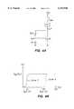
- FIG. 1Ashows a first embodiment according to the present invention.
- FIG. 1Bshows two curves illustrating the operation of the first embodiment under different conditions.
- a capacitor C1is coupled to a voltage source VDD and is also to be coupled to a positive coefficient temperature (PTC) device Rp1 via a switch SW1.
- Rp1is coupled to a gate electrode of an n-channel enhancement type, MOSFET Q1.
- a load RL1is coupled between voltage source VDD and a drain electrode of transistor Q1.
- Transistor Q1has its source electrode coupled to the ground.
- transistor Q1when power is applied (i.e., when SW1 is closed), transistor Q1 is turned on and then turned off after a predetermined on-duration. If there is a change in condition, such as occurrence of an overload or overheat, which is thermally sensed by Rp1, the on-duration will be longer, i.e., the turn-off time will be later than under the normal condition, as will be described below in detail.
- Rp1is a polymeric PTC resistor, such as PolySwitch® device manufactured by Raychem Corporation, Menlo Park, Calif.
- its resistance valuemay change from, for instance, 1 ohm at 25° C. to 100M ohms at 150° C., an 8 order of magnitude change.
- C1is equal to 1 ⁇ F
- Other types of PTC devicemay also be used.
- FIG. 2Ashows a second embodiment according to the present invention.
- This second embodimentis a variation of the first embodiment in FIG. 1A. Its operation is similarly illustrated by the two curves in FIG. 2B.
- a load RL2has one end coupled to a switch SW2 and the other end coupled to a drain electrode of an n-channel enhancement type, MOSFET Q2.
- Switch SW2is coupled to voltage source VDD.
- a capacitor C2is coupled between the drain and gate electrodes of transistor Q2.
- a PTC device Rp2is coupled between the gate electrode of transistor Q2 and the ground.
- Transistor Q2has its source electrode coupled to the ground.
- Rp2is a polymeric PTC resistor, such as PolySwitch® device manufactured by Raychem Corporation, Menlo Park, Calif.
- its resistance valuemay change from, for instance, 1 ohm at 25° C. to 100M ohms at 150° C., an 8 order of magnitude change.
- C2is equal to 1 ⁇ F
- Other types of PTC devicemay also be used.
- FIG. 3Ashows a third embodiment according to the present invention.
- FIG. 3Bshows two curves illustrating the operation of the third embodiment under different conditions.
- a PTC device Rp3is coupled between voltage source VDD and a switch SW3, which is coupled to a gate electrode of an n-channel, enhancement type MOSFET Q3.
- a capacitor C3is coupled between the gate electrode of the transistor Q3 and the ground.
- a load RL3is coupled between voltage source VDD and a drain electrode of transistor Q3.
- a source electrode of transistor Q3is coupled to the ground.
- transistor Q3when power is applied (i.e., SW3 is closed), transistor Q3 is turned off and then turned on after a predetermined off-duration. If there is a change in condition, such as occurrence of an overload or overheat, the off-duration will be longer, i.e., the turn-on time will be later than under the normal condition, as will be described below in detail.
- Vg3As capacitor C3 charges up gradually, the gate voltage Vg3 increases, causing the current Io3 to gradually increase. Eventually, after a time period of Rp3•C3, when capacitor C3 is; fully charged, Vg3 becomes equal to VDD. As a result, the output current flowing in load RL3 is at a maximum level of VDD/RL3, as illustrated by curve 5 in FIG. 3B.
- Rp3is a polymeric PTC resistor, such as PolySwitch® device manufactured by Raychem Corporation, Menlo Park, Calif.
- its resistance valuemay change from, for instance, 1 ohm at 25° C. to 100M ohms at 150° C., an 8 order of magnitude change.
- C3is equal to 1 ⁇ F
- Other types of PTC devicemay also be used.
- FIG. 4Ashows a fourth embodiment according to the present invention.
- This embodimentis a variation of the third embodiment in FIG. 3A. Its operation is similarly illustrated by the two curves in FIG. 4B.
- a load RL4is coupled between a switch SW4 and a drain electrode of an n-channel enhancement type, MOSFET Q4.
- Switch SW4is coupled to voltage source VDD.
- a PTC device Rp4is coupled between a load RL4 and a gate electrode of transistor Q4.
- a capacitor C4is coupled between the drain and gate electrodes of transistor Q4.
- the source electrode of transistor Q4is coupled to the ground.
- Rp4is a polymeric PTC resistor, such as PolySwitch® device manufactured by Raychem Corporation, Menlo Park, Calif.
- its resistance valuemay change from, for instance, 1 ohm at 25° C. to 100M ohms at 150° C., an 8 order of magnitude change.
- C4is equal to 1 ⁇ F
- Other types of PTC devicemay also be used.
- a resistormay also be connected in series with the PTC device in the first and second embodiments for adjusting the on-duration ranges of the transistors.
- a negative temperature coefficient (NTC) devicemay be used in place of the PTC device with appropriate changes in the polarities.
Landscapes
- Electronic Switches (AREA)
- Emergency Protection Circuit Devices (AREA)
Abstract
Description
Claims (21)
Priority Applications (7)
| Application Number | Priority Date | Filing Date | Title |
|---|---|---|---|
| US09/133,334US6153948A (en) | 1998-08-13 | 1998-08-13 | Electronic circuits with wide dynamic range of on/off delay time |
| EP99939012AEP1105969B9 (en) | 1998-08-13 | 1999-08-05 | Electronic circuits with wide dynamic range of on/off delay time |
| PCT/US1999/017719WO2000010249A1 (en) | 1998-08-13 | 1999-08-05 | Electronic circuits with wide dynamic range of on/off delay time |
| CNB998096342ACN1149736C (en) | 1998-08-13 | 1999-08-05 | Electronic circuit with wide dynamic range of on/off delay time |
| DE69940605TDE69940605D1 (en) | 1998-08-13 | 1999-08-05 | ELECTRONIC CIRCUITS WITH LARGE DYNAMIC RANGE OF ON / OFF DELAYS |
| JP2000565603AJP2002523912A (en) | 1998-08-13 | 1999-08-05 | Electronic circuit with wide dynamic range on or off delay |
| TW088113804ATW475320B (en) | 1998-08-13 | 1999-08-12 | Electronic circuits with wide dynamic range of on/off delay time and method therefor |
Applications Claiming Priority (1)
| Application Number | Priority Date | Filing Date | Title |
|---|---|---|---|
| US09/133,334US6153948A (en) | 1998-08-13 | 1998-08-13 | Electronic circuits with wide dynamic range of on/off delay time |
Publications (1)
| Publication Number | Publication Date |
|---|---|
| US6153948Atrue US6153948A (en) | 2000-11-28 |
Family
ID=22458096
Family Applications (1)
| Application Number | Title | Priority Date | Filing Date |
|---|---|---|---|
| US09/133,334Expired - Fee RelatedUS6153948A (en) | 1998-08-13 | 1998-08-13 | Electronic circuits with wide dynamic range of on/off delay time |
Country Status (7)
| Country | Link |
|---|---|
| US (1) | US6153948A (en) |
| EP (1) | EP1105969B9 (en) |
| JP (1) | JP2002523912A (en) |
| CN (1) | CN1149736C (en) |
| DE (1) | DE69940605D1 (en) |
| TW (1) | TW475320B (en) |
| WO (1) | WO2000010249A1 (en) |
Cited By (6)
| Publication number | Priority date | Publication date | Assignee | Title |
|---|---|---|---|---|
| US6509658B1 (en)* | 1998-12-16 | 2003-01-21 | Jinnes Technologies Inc. | Device for the automatic shut-off of equipment's stand-by power |
| US6670881B1 (en) | 2001-07-27 | 2003-12-30 | General Electric Company | Positive temperature coefficient resistor/overload resistor method and assemblies |
| WO2005059936A3 (en)* | 2003-12-11 | 2007-02-22 | Joslyn Hi Voltage Corp | Electrical, transmission/substation/distribution shunt capacitor switching and control system with integrated, automatically resettable, overcurrent protection |
| CN102811041A (en)* | 2012-07-13 | 2012-12-05 | 电子科技大学 | a long delay circuit |
| US20140159687A1 (en)* | 2012-12-07 | 2014-06-12 | Samsung Electronics Co., Ltd. | Adaptive Power Converters and Methods of Operating the Same |
| DE102013112261A1 (en)* | 2013-11-07 | 2015-05-07 | Semikron Elektronik Gmbh & Co. Kg | Power semiconductor circuit |
Families Citing this family (3)
| Publication number | Priority date | Publication date | Assignee | Title |
|---|---|---|---|---|
| US7075343B2 (en)* | 2004-12-07 | 2006-07-11 | Analog Devices, Inc. | Self-timed switching regulator pre-driver |
| CN101242172B (en)* | 2007-02-08 | 2010-05-19 | 佛山市顺德区顺达电脑厂有限公司 | Delay circuit |
| CN107980206A (en)* | 2017-01-03 | 2018-05-01 | 深圳配天智能技术研究院有限公司 | Multi-channel delay control device and control power supply |
Citations (11)
| Publication number | Priority date | Publication date | Assignee | Title |
|---|---|---|---|---|
| US3737732A (en)* | 1970-09-01 | 1973-06-05 | Matsushita Electric Works Ltd | Time delay relay |
| US4001610A (en)* | 1975-06-30 | 1977-01-04 | Ordnance Research, Inc. | Time delay circuit |
| US4035669A (en)* | 1974-12-25 | 1977-07-12 | Nippon Gakki Seizo Kabushiki Kaisha | Operation-delayed switching circuit |
| FR2342571A1 (en)* | 1976-02-24 | 1977-09-23 | Klaxon Sa | DC motor overload protection circuit - is for vehicle window operation and reverses motor operation when obstructed |
| US4160192A (en)* | 1977-06-03 | 1979-07-03 | Mcallise Raymond J | Delayed turn-off switching circuit |
| GB2040121A (en)* | 1978-11-21 | 1980-08-20 | Redring Electric Ltd | Power control circuits |
| US4686383A (en)* | 1983-08-10 | 1987-08-11 | British Telecommunications Public Limited Company | Electronic switch with automatic protective turn-off followed by automatic reset |
| US4686386A (en)* | 1984-03-21 | 1987-08-11 | Oki Electric Industry Co., Ltd. | Power-down circuits for dynamic MOS integrated circuits |
| US4777379A (en)* | 1984-11-02 | 1988-10-11 | Young Danny J | Power cycling apparatus |
| US4801822A (en)* | 1986-08-11 | 1989-01-31 | Matsushita Electric Works, Ltd. | Semiconductor switching circuit |
| US5187632A (en)* | 1991-07-09 | 1993-02-16 | Daimler-Benz Ag | Controllable semiconductor switching device having integrated current limitation and overheating disconnection |
Family Cites Families (2)
| Publication number | Priority date | Publication date | Assignee | Title |
|---|---|---|---|---|
| SE470530B (en)* | 1992-11-16 | 1994-07-04 | Ericsson Telefon Ab L M | limiter |
| DE19742930C1 (en)* | 1997-09-29 | 1998-11-19 | Siemens Ag | Power switch with overload protection |
- 1998
- 1998-08-13USUS09/133,334patent/US6153948A/ennot_activeExpired - Fee Related
- 1999
- 1999-08-05JPJP2000565603Apatent/JP2002523912A/enactivePending
- 1999-08-05EPEP99939012Apatent/EP1105969B9/ennot_activeExpired - Lifetime
- 1999-08-05DEDE69940605Tpatent/DE69940605D1/ennot_activeExpired - Fee Related
- 1999-08-05CNCNB998096342Apatent/CN1149736C/ennot_activeExpired - Fee Related
- 1999-08-05WOPCT/US1999/017719patent/WO2000010249A1/enactiveApplication Filing
- 1999-08-12TWTW088113804Apatent/TW475320B/ennot_activeIP Right Cessation
Patent Citations (11)
| Publication number | Priority date | Publication date | Assignee | Title |
|---|---|---|---|---|
| US3737732A (en)* | 1970-09-01 | 1973-06-05 | Matsushita Electric Works Ltd | Time delay relay |
| US4035669A (en)* | 1974-12-25 | 1977-07-12 | Nippon Gakki Seizo Kabushiki Kaisha | Operation-delayed switching circuit |
| US4001610A (en)* | 1975-06-30 | 1977-01-04 | Ordnance Research, Inc. | Time delay circuit |
| FR2342571A1 (en)* | 1976-02-24 | 1977-09-23 | Klaxon Sa | DC motor overload protection circuit - is for vehicle window operation and reverses motor operation when obstructed |
| US4160192A (en)* | 1977-06-03 | 1979-07-03 | Mcallise Raymond J | Delayed turn-off switching circuit |
| GB2040121A (en)* | 1978-11-21 | 1980-08-20 | Redring Electric Ltd | Power control circuits |
| US4686383A (en)* | 1983-08-10 | 1987-08-11 | British Telecommunications Public Limited Company | Electronic switch with automatic protective turn-off followed by automatic reset |
| US4686386A (en)* | 1984-03-21 | 1987-08-11 | Oki Electric Industry Co., Ltd. | Power-down circuits for dynamic MOS integrated circuits |
| US4777379A (en)* | 1984-11-02 | 1988-10-11 | Young Danny J | Power cycling apparatus |
| US4801822A (en)* | 1986-08-11 | 1989-01-31 | Matsushita Electric Works, Ltd. | Semiconductor switching circuit |
| US5187632A (en)* | 1991-07-09 | 1993-02-16 | Daimler-Benz Ag | Controllable semiconductor switching device having integrated current limitation and overheating disconnection |
Non-Patent Citations (1)
| Title |
|---|
| International Search Report for International Application No. PCT/US99/17719 dated Nov. 19, 1999.* |
Cited By (9)
| Publication number | Priority date | Publication date | Assignee | Title |
|---|---|---|---|---|
| US6509658B1 (en)* | 1998-12-16 | 2003-01-21 | Jinnes Technologies Inc. | Device for the automatic shut-off of equipment's stand-by power |
| US6670881B1 (en) | 2001-07-27 | 2003-12-30 | General Electric Company | Positive temperature coefficient resistor/overload resistor method and assemblies |
| WO2005059936A3 (en)* | 2003-12-11 | 2007-02-22 | Joslyn Hi Voltage Corp | Electrical, transmission/substation/distribution shunt capacitor switching and control system with integrated, automatically resettable, overcurrent protection |
| CN102811041A (en)* | 2012-07-13 | 2012-12-05 | 电子科技大学 | a long delay circuit |
| CN102811041B (en)* | 2012-07-13 | 2016-02-03 | 电子科技大学 | A kind of Long-time-delay circuit |
| US20140159687A1 (en)* | 2012-12-07 | 2014-06-12 | Samsung Electronics Co., Ltd. | Adaptive Power Converters and Methods of Operating the Same |
| US9369046B2 (en)* | 2012-12-07 | 2016-06-14 | Samsung Electronics Co., Ltd. | Power converters with adaptive slew rate and methods of operating same |
| DE102013112261A1 (en)* | 2013-11-07 | 2015-05-07 | Semikron Elektronik Gmbh & Co. Kg | Power semiconductor circuit |
| DE102013112261B4 (en) | 2013-11-07 | 2023-01-26 | Semikron Elektronik Gmbh & Co. Kg | power semiconductor circuit |
Also Published As
| Publication number | Publication date |
|---|---|
| TW475320B (en) | 2002-02-01 |
| JP2002523912A (en) | 2002-07-30 |
| WO2000010249A1 (en) | 2000-02-24 |
| EP1105969B1 (en) | 2009-03-18 |
| EP1105969B9 (en) | 2009-09-09 |
| CN1149736C (en) | 2004-05-12 |
| DE69940605D1 (en) | 2009-04-30 |
| EP1105969A1 (en) | 2001-06-13 |
| CN1312972A (en) | 2001-09-12 |
Similar Documents
| Publication | Publication Date | Title |
|---|---|---|
| JP2841104B2 (en) | Internal current limiting circuit in high-speed high-potential side power switch | |
| US5506539A (en) | IGFET power semiconductor circuit with GAE control and fault detection circuits | |
| US5914545A (en) | Switching device with power FET and short-circuit detection | |
| US6181541B1 (en) | Transistor-PTC circuit protection devices | |
| US7701686B2 (en) | Power supply controller | |
| US6153948A (en) | Electronic circuits with wide dynamic range of on/off delay time | |
| CA2179466A1 (en) | Protection element and method for protecting a circuit | |
| US6067219A (en) | Power cut-off device | |
| JP2001216033A (en) | Power supply control device and power supply control method | |
| EP0702455A2 (en) | Overheat protection apparatus for self-turn-off device | |
| CN1669118B (en) | Method of protecting semiconductor device and protection apparatus for semiconductor device using the same | |
| US4467386A (en) | Fail-safe sensor circuit | |
| CN1269893A (en) | Circuit arrangement and method for protecting control element against overcurrent | |
| US20070035906A1 (en) | Transient blocking unit | |
| US7369387B2 (en) | Apparatus and method for temperature-dependent transient blocking | |
| US4983897A (en) | Control circuit | |
| JPH07221261A (en) | Power semiconductor device with temperature sensor | |
| KR20050015387A (en) | Protection circuit system for motor control unit in electric vehicle | |
| RU2242831C2 (en) | Voltage switching device incorporating load unit overcurrent protective gear | |
| JP2000315588A (en) | Power supply control device | |
| CN218976325U (en) | Overcurrent protection circuit, power supply circuit and electronic equipment | |
| US12261597B2 (en) | Capacitor charging method, corresponding circuit and device | |
| JP3772516B2 (en) | Current limit circuit | |
| JPH03164027A (en) | Overcurrent protective circuit | |
| FR3089360A1 (en) | Electronic dimmer for low voltage circuit |
Legal Events
| Date | Code | Title | Description |
|---|---|---|---|
| AS | Assignment | Owner name:RAYCHEM CORPORATION, CALIFORNIA Free format text:ASSIGNMENT OF ASSIGNORS INTEREST;ASSIGNORS:COGAN, ADRIAN I.;SOURI, SHUKRI J.;REEL/FRAME:009393/0970 Effective date:19980813 | |
| AS | Assignment | Owner name:TYCO INTERNATIONAL LTD., A CORPORATION OF BERMUDA, Free format text:MERGER & REORGANIZATION;ASSIGNOR:RAYCHEM CORPORATION, A CORPORATION OF DELAWARE;REEL/FRAME:011682/0001 Effective date:19990812 Owner name:AMP INCORPORATED, A CORPORATION OF PENNSYLVANIA, P Free format text:MERGER & REORGANIZATION;ASSIGNOR:RAYCHEM CORPORATION, A CORPORATION OF DELAWARE;REEL/FRAME:011682/0001 Effective date:19990812 Owner name:TYCO INTERNATIONAL (PA), INC., A CORPORATION OF NE Free format text:MERGER & REORGANIZATION;ASSIGNOR:RAYCHEM CORPORATION, A CORPORATION OF DELAWARE;REEL/FRAME:011682/0001 Effective date:19990812 | |
| AS | Assignment | Owner name:TYCO ELECTRONICS CORPORATION, A CORPORATION OF PEN Free format text:CHANGE OF NAME;ASSIGNOR:AMP INCORPORATED, A CORPORATION OF PENNSYLVANIA;REEL/FRAME:011675/0436 Effective date:19990913 | |
| FPAY | Fee payment | Year of fee payment:4 | |
| FPAY | Fee payment | Year of fee payment:8 | |
| REMI | Maintenance fee reminder mailed | ||
| LAPS | Lapse for failure to pay maintenance fees | ||
| LAPS | Lapse for failure to pay maintenance fees | Free format text:PATENT EXPIRED FOR FAILURE TO PAY MAINTENANCE FEES (ORIGINAL EVENT CODE: EXP.); ENTITY STATUS OF PATENT OWNER: LARGE ENTITY | |
| STCH | Information on status: patent discontinuation | Free format text:PATENT EXPIRED DUE TO NONPAYMENT OF MAINTENANCE FEES UNDER 37 CFR 1.362 | |
| FP | Lapsed due to failure to pay maintenance fee | Effective date:20121128 | |
| AS | Assignment | Owner name:LITTELFUSE, INC., ILLINOIS Free format text:ASSIGNMENT OF ASSIGNORS INTEREST;ASSIGNOR:TYCO ELECTRONICS CORPORATION;REEL/FRAME:039392/0693 Effective date:20160325 |