US6153929A - Low profile multi-IC package connector - Google Patents
Low profile multi-IC package connectorDownload PDFInfo
- Publication number
- US6153929A US6153929AUS09/138,372US13837298AUS6153929AUS 6153929 AUS6153929 AUS 6153929AUS 13837298 AUS13837298 AUS 13837298AUS 6153929 AUS6153929 AUS 6153929A
- Authority
- US
- United States
- Prior art keywords
- chip package
- cage
- packages
- package
- conductive
- Prior art date
- Legal status (The legal status is an assumption and is not a legal conclusion. Google has not performed a legal analysis and makes no representation as to the accuracy of the status listed.)
- Expired - Lifetime
Links
Images


Classifications
- H—ELECTRICITY
- H05—ELECTRIC TECHNIQUES NOT OTHERWISE PROVIDED FOR
- H05K—PRINTED CIRCUITS; CASINGS OR CONSTRUCTIONAL DETAILS OF ELECTRIC APPARATUS; MANUFACTURE OF ASSEMBLAGES OF ELECTRICAL COMPONENTS
- H05K1/00—Printed circuits
- H05K1/18—Printed circuits structurally associated with non-printed electric components
- H05K1/181—Printed circuits structurally associated with non-printed electric components associated with surface mounted components
- H—ELECTRICITY
- H01—ELECTRIC ELEMENTS
- H01L—SEMICONDUCTOR DEVICES NOT COVERED BY CLASS H10
- H01L25/00—Assemblies consisting of a plurality of semiconductor or other solid state devices
- H01L25/03—Assemblies consisting of a plurality of semiconductor or other solid state devices all the devices being of a type provided for in a single subclass of subclasses H10B, H10D, H10F, H10H, H10K or H10N, e.g. assemblies of rectifier diodes
- H01L25/10—Assemblies consisting of a plurality of semiconductor or other solid state devices all the devices being of a type provided for in a single subclass of subclasses H10B, H10D, H10F, H10H, H10K or H10N, e.g. assemblies of rectifier diodes the devices having separate containers
- H01L25/105—Assemblies consisting of a plurality of semiconductor or other solid state devices all the devices being of a type provided for in a single subclass of subclasses H10B, H10D, H10F, H10H, H10K or H10N, e.g. assemblies of rectifier diodes the devices having separate containers the devices being integrated devices of class H10
- H—ELECTRICITY
- H01—ELECTRIC ELEMENTS
- H01L—SEMICONDUCTOR DEVICES NOT COVERED BY CLASS H10
- H01L2225/00—Details relating to assemblies covered by the group H01L25/00 but not provided for in its subgroups
- H01L2225/03—All the devices being of a type provided for in the same main group of the same subclass of class H10, e.g. assemblies of rectifier diodes
- H01L2225/10—All the devices being of a type provided for in the same main group of the same subclass of class H10, e.g. assemblies of rectifier diodes the devices having separate containers
- H01L2225/1005—All the devices being of a type provided for in the same main group of the same subclass of class H10, e.g. assemblies of rectifier diodes the devices having separate containers the devices being integrated devices of class H10
- H01L2225/1011—All the devices being of a type provided for in the same main group of the same subclass of class H10, e.g. assemblies of rectifier diodes the devices having separate containers the devices being integrated devices of class H10 the containers being in a stacked arrangement
- H01L2225/1017—All the devices being of a type provided for in the same main group of the same subclass of class H10, e.g. assemblies of rectifier diodes the devices having separate containers the devices being integrated devices of class H10 the containers being in a stacked arrangement the lowermost container comprising a device support
- H01L2225/1029—All the devices being of a type provided for in the same main group of the same subclass of class H10, e.g. assemblies of rectifier diodes the devices having separate containers the devices being integrated devices of class H10 the containers being in a stacked arrangement the lowermost container comprising a device support the support being a lead frame
- H—ELECTRICITY
- H01—ELECTRIC ELEMENTS
- H01L—SEMICONDUCTOR DEVICES NOT COVERED BY CLASS H10
- H01L2225/00—Details relating to assemblies covered by the group H01L25/00 but not provided for in its subgroups
- H01L2225/03—All the devices being of a type provided for in the same main group of the same subclass of class H10, e.g. assemblies of rectifier diodes
- H01L2225/10—All the devices being of a type provided for in the same main group of the same subclass of class H10, e.g. assemblies of rectifier diodes the devices having separate containers
- H01L2225/1005—All the devices being of a type provided for in the same main group of the same subclass of class H10, e.g. assemblies of rectifier diodes the devices having separate containers the devices being integrated devices of class H10
- H01L2225/1011—All the devices being of a type provided for in the same main group of the same subclass of class H10, e.g. assemblies of rectifier diodes the devices having separate containers the devices being integrated devices of class H10 the containers being in a stacked arrangement
- H01L2225/1047—Details of electrical connections between containers
- H01L2225/1064—Electrical connections provided on a side surface of one or more of the containers
- H—ELECTRICITY
- H01—ELECTRIC ELEMENTS
- H01L—SEMICONDUCTOR DEVICES NOT COVERED BY CLASS H10
- H01L2225/00—Details relating to assemblies covered by the group H01L25/00 but not provided for in its subgroups
- H01L2225/03—All the devices being of a type provided for in the same main group of the same subclass of class H10, e.g. assemblies of rectifier diodes
- H01L2225/10—All the devices being of a type provided for in the same main group of the same subclass of class H10, e.g. assemblies of rectifier diodes the devices having separate containers
- H01L2225/1005—All the devices being of a type provided for in the same main group of the same subclass of class H10, e.g. assemblies of rectifier diodes the devices having separate containers the devices being integrated devices of class H10
- H01L2225/1011—All the devices being of a type provided for in the same main group of the same subclass of class H10, e.g. assemblies of rectifier diodes the devices having separate containers the devices being integrated devices of class H10 the containers being in a stacked arrangement
- H01L2225/1047—Details of electrical connections between containers
- H01L2225/107—Indirect electrical connections, e.g. via an interposer, a flexible substrate, using TAB
- H—ELECTRICITY
- H01—ELECTRIC ELEMENTS
- H01L—SEMICONDUCTOR DEVICES NOT COVERED BY CLASS H10
- H01L2225/00—Details relating to assemblies covered by the group H01L25/00 but not provided for in its subgroups
- H01L2225/03—All the devices being of a type provided for in the same main group of the same subclass of class H10, e.g. assemblies of rectifier diodes
- H01L2225/10—All the devices being of a type provided for in the same main group of the same subclass of class H10, e.g. assemblies of rectifier diodes the devices having separate containers
- H01L2225/1005—All the devices being of a type provided for in the same main group of the same subclass of class H10, e.g. assemblies of rectifier diodes the devices having separate containers the devices being integrated devices of class H10
- H01L2225/1011—All the devices being of a type provided for in the same main group of the same subclass of class H10, e.g. assemblies of rectifier diodes the devices having separate containers the devices being integrated devices of class H10 the containers being in a stacked arrangement
- H01L2225/1094—Thermal management, e.g. cooling
- H—ELECTRICITY
- H01—ELECTRIC ELEMENTS
- H01L—SEMICONDUCTOR DEVICES NOT COVERED BY CLASS H10
- H01L2924/00—Indexing scheme for arrangements or methods for connecting or disconnecting semiconductor or solid-state bodies as covered by H01L24/00
- H01L2924/0001—Technical content checked by a classifier
- H01L2924/0002—Not covered by any one of groups H01L24/00, H01L24/00 and H01L2224/00
- H—ELECTRICITY
- H01—ELECTRIC ELEMENTS
- H01L—SEMICONDUCTOR DEVICES NOT COVERED BY CLASS H10
- H01L2924/00—Indexing scheme for arrangements or methods for connecting or disconnecting semiconductor or solid-state bodies as covered by H01L24/00
- H01L2924/30—Technical effects
- H01L2924/301—Electrical effects
- H01L2924/3011—Impedance
- H—ELECTRICITY
- H05—ELECTRIC TECHNIQUES NOT OTHERWISE PROVIDED FOR
- H05K—PRINTED CIRCUITS; CASINGS OR CONSTRUCTIONAL DETAILS OF ELECTRIC APPARATUS; MANUFACTURE OF ASSEMBLAGES OF ELECTRICAL COMPONENTS
- H05K1/00—Printed circuits
- H05K1/02—Details
- H05K1/14—Structural association of two or more printed circuits
- H05K1/145—Arrangements wherein electric components are disposed between and simultaneously connected to two planar printed circuit boards, e.g. Cordwood modules
- H—ELECTRICITY
- H05—ELECTRIC TECHNIQUES NOT OTHERWISE PROVIDED FOR
- H05K—PRINTED CIRCUITS; CASINGS OR CONSTRUCTIONAL DETAILS OF ELECTRIC APPARATUS; MANUFACTURE OF ASSEMBLAGES OF ELECTRICAL COMPONENTS
- H05K1/00—Printed circuits
- H05K1/02—Details
- H05K1/14—Structural association of two or more printed circuits
- H05K1/147—Structural association of two or more printed circuits at least one of the printed circuits being bent or folded, e.g. by using a flexible printed circuit
- H—ELECTRICITY
- H05—ELECTRIC TECHNIQUES NOT OTHERWISE PROVIDED FOR
- H05K—PRINTED CIRCUITS; CASINGS OR CONSTRUCTIONAL DETAILS OF ELECTRIC APPARATUS; MANUFACTURE OF ASSEMBLAGES OF ELECTRICAL COMPONENTS
- H05K2201/00—Indexing scheme relating to printed circuits covered by H05K1/00
- H05K2201/04—Assemblies of printed circuits
- H05K2201/049—PCB for one component, e.g. for mounting onto mother PCB
- H—ELECTRICITY
- H05—ELECTRIC TECHNIQUES NOT OTHERWISE PROVIDED FOR
- H05K—PRINTED CIRCUITS; CASINGS OR CONSTRUCTIONAL DETAILS OF ELECTRIC APPARATUS; MANUFACTURE OF ASSEMBLAGES OF ELECTRICAL COMPONENTS
- H05K2201/00—Indexing scheme relating to printed circuits covered by H05K1/00
- H05K2201/10—Details of components or other objects attached to or integrated in a printed circuit board
- H05K2201/10431—Details of mounted components
- H05K2201/10507—Involving several components
- H05K2201/10515—Stacked components
- H—ELECTRICITY
- H05—ELECTRIC TECHNIQUES NOT OTHERWISE PROVIDED FOR
- H05K—PRINTED CIRCUITS; CASINGS OR CONSTRUCTIONAL DETAILS OF ELECTRIC APPARATUS; MANUFACTURE OF ASSEMBLAGES OF ELECTRICAL COMPONENTS
- H05K2201/00—Indexing scheme relating to printed circuits covered by H05K1/00
- H05K2201/10—Details of components or other objects attached to or integrated in a printed circuit board
- H05K2201/10613—Details of electrical connections of non-printed components, e.g. special leads
- H05K2201/10621—Components characterised by their electrical contacts
- H05K2201/10689—Leaded Integrated Circuit [IC] package, e.g. dual-in-line [DIL]
- Y—GENERAL TAGGING OF NEW TECHNOLOGICAL DEVELOPMENTS; GENERAL TAGGING OF CROSS-SECTIONAL TECHNOLOGIES SPANNING OVER SEVERAL SECTIONS OF THE IPC; TECHNICAL SUBJECTS COVERED BY FORMER USPC CROSS-REFERENCE ART COLLECTIONS [XRACs] AND DIGESTS
- Y02—TECHNOLOGIES OR APPLICATIONS FOR MITIGATION OR ADAPTATION AGAINST CLIMATE CHANGE
- Y02P—CLIMATE CHANGE MITIGATION TECHNOLOGIES IN THE PRODUCTION OR PROCESSING OF GOODS
- Y02P70/00—Climate change mitigation technologies in the production process for final industrial or consumer products
- Y02P70/50—Manufacturing or production processes characterised by the final manufactured product
- Y—GENERAL TAGGING OF NEW TECHNOLOGICAL DEVELOPMENTS; GENERAL TAGGING OF CROSS-SECTIONAL TECHNOLOGIES SPANNING OVER SEVERAL SECTIONS OF THE IPC; TECHNICAL SUBJECTS COVERED BY FORMER USPC CROSS-REFERENCE ART COLLECTIONS [XRACs] AND DIGESTS
- Y10—TECHNICAL SUBJECTS COVERED BY FORMER USPC
- Y10T—TECHNICAL SUBJECTS COVERED BY FORMER US CLASSIFICATION
- Y10T29/00—Metal working
- Y10T29/49—Method of mechanical manufacture
- Y10T29/49002—Electrical device making
- Y10T29/49117—Conductor or circuit manufacturing
- Y10T29/49124—On flat or curved insulated base, e.g., printed circuit, etc.
- Y10T29/49126—Assembling bases
- Y—GENERAL TAGGING OF NEW TECHNOLOGICAL DEVELOPMENTS; GENERAL TAGGING OF CROSS-SECTIONAL TECHNOLOGIES SPANNING OVER SEVERAL SECTIONS OF THE IPC; TECHNICAL SUBJECTS COVERED BY FORMER USPC CROSS-REFERENCE ART COLLECTIONS [XRACs] AND DIGESTS
- Y10—TECHNICAL SUBJECTS COVERED BY FORMER USPC
- Y10T—TECHNICAL SUBJECTS COVERED BY FORMER US CLASSIFICATION
- Y10T29/00—Metal working
- Y10T29/49—Method of mechanical manufacture
- Y10T29/49002—Electrical device making
- Y10T29/49117—Conductor or circuit manufacturing
- Y10T29/49124—On flat or curved insulated base, e.g., printed circuit, etc.
- Y10T29/4913—Assembling to base an electrical component, e.g., capacitor, etc.
- Y—GENERAL TAGGING OF NEW TECHNOLOGICAL DEVELOPMENTS; GENERAL TAGGING OF CROSS-SECTIONAL TECHNOLOGIES SPANNING OVER SEVERAL SECTIONS OF THE IPC; TECHNICAL SUBJECTS COVERED BY FORMER USPC CROSS-REFERENCE ART COLLECTIONS [XRACs] AND DIGESTS
- Y10—TECHNICAL SUBJECTS COVERED BY FORMER USPC
- Y10T—TECHNICAL SUBJECTS COVERED BY FORMER US CLASSIFICATION
- Y10T29/00—Metal working
- Y10T29/49—Method of mechanical manufacture
- Y10T29/49002—Electrical device making
- Y10T29/49117—Conductor or circuit manufacturing
- Y10T29/49169—Assembling electrical component directly to terminal or elongated conductor
Definitions
- This inventionrelates generally to semiconductor device assemblies having molded housings. More particularly, the invention relates to connectors for joining a stack of packaged devices into a small multi-IC chip assembly package operable at high speeds.
- the evolution of the computerhas resulted in a requirement for greatly increased memory capacity in much smaller packages. Another requirement is the capability for reliable operation at much higher clock speeds, e.g. up to 800 MHz or more.
- the memory device(s)must be readily produced in high quantity and at low cost with reduced rates of failure or rejection.
- One way to provide a greater memory storage capacity in a smaller spaceis by stacking a plurality of memory chips and interconnecting them to produce a limited number of connections to e.g. a circuit board. In so doing, a number of factors must be addressed, including heat dissipation, ease of interconnection, impedance effects, etc.
- MCMmulti-chip modules
- diceare stacked vertically on opposite sides of a substrate, for example, or atop each other with intervening insulative layers, prior to encapsulation. Examples of such devices are shown in U.S. Pat. No. 5,239,198 to Lin et al., U.S. Pat. No. 5,323,060 to Fogal et al. and U.S. Pat. No. 5,495,398 to Takiar et al.
- U.S. Pat. No. 5,604,377discloses a rack with multiple shelves for holding unpackaged chips.
- the chipsare electrically connected by lead frames to a wiring interface on a vertical circuit board which can be connected to a PCB.
- the entire assemblyis contained in a sealed enclosure.
- U.S. Pat. No. 5,637,912discloses a multi-chip module in which chips are stacked in a vertical arrangement, and a metallization pattern deposited on a surface formed by the chip edges.
- MCM devicesare also made which combine a number of dice side-by-side on a substrate.
- the conventional single in-line multi-chip module (SIMM) and dual in-line multi-chip modules (DIMM)are common examples of this MCM configuration.
- Other examplesare shown in U.S. Pat. No. 5,137,836 to Lam, U.S. Pat. Nos. 4,992,849 and 4,992,850 to Corbett et al., U.S. Pat. No. 5,255,156 to Chang, U.S. Pat. Nos. 5,239,747 and 5,461,544 to Ewers, U.S. Pat. No. 5,465,470 to Vongfuangfoo et al., and U.S. Pat. No. 5,480,840 to Barnes et al.
- U.S. Pat. No. 5,592,019 to Ueda et al.shows multiple single-chip packages connected on end to a substrate by their leads.
- a stackable carrier for chipsis shown in U.S. Pat. No. 4,996,587 to Hinrichsmeyer et al.
- a single chip or dieis adhesively positioned in an underside recess in the carrier and conductive wires from the die are passed through a hole and bonded to conductors formed on the upper surface of the carrier.
- S-shaped connector clipsare soldered to each of the I/O leads on opposed edges of the carrier and to the clips of other carriers stacked with it to form a multi-chip package (MCM).
- MCMmulti-chip package
- a multi-chip memory modulehas a plurality of stacked IC devices between opposing "side boards", the latter comprising circuit boards with a pattern of interconnected vias into which the pins of the devices are soldered.
- the pins of the lowermost deviceare also soldered to the substrate, such as a main circuit board, and comprise the interconnection between the module and the circuit board.
- U.S. Pat. No. 5,420,751 to Burnsdiscloses a stacked IC package which has vertical metal rails which pass through a cap above the packaged devices. Each rail is soldered to corresponding outer leads of the primary packages and has a lower end connectable to a PCB. The primary devices are adhesively joined to prevent movement of the devices in the stack package. Manufacture of the rails is a complex process, and the manipulation of a large number of parts to form the multi-IC package may be counterproductive.
- a stack package for thin small outline package (TSOP) devicesis shown with vertical metal rails for each set of corresponding outer leads of the TSOP devices.
- a secondary "lead frame" for each TSOP packagehas secondary leads which are soldered to the pins of the TSOP package and to the metal rails.
- Each secondary leadis particularly formed with a "flex offset" to provide a stress relief connection with the rail.
- the Burns apparatusrequires a second lead frame for each packaged primary device. Furthermore, additional steps are required to form the stress relief offset. Furthermore, maintaining the rails in parallel non-contact alignment during and following soldering appears to be a major problem. A large number of soldering steps is required to join the large number of parts.
- the multi-chip moduleis complex to make, using a large number of parts which must be formed, aligned and individually secured in the device.
- the y-dimension (perpendicular to the host PCB) of the multi-chip moduleis relatively great, and may be excessive for the particular end use.
- the leads and connectionsresult in excessive impedance effects at high clock speeds, i.e. greater than about 400 MHz, and particularly at speeds now anticipated, i.e. about 800 MHz and higher.
- thermal expansionWith multi-chip devices in particular, elasticity is required in the electrical connections to accommodate thermal expansion, as well as dimensional variation in the primary devices.
- U.S. Pat. No. 5,600,183 to Gates, Jr.discloses a conductive adhesive comprising a mixture of e.g. silver powder in an epoxy material.
- U.S. Pat. No. 5,468,655 to Greerdiscloses a temporary electrical connection comprising a metal paste applied to contact pads, then heated to partially melt the metal. A solder bump may then be placed in contact with the metal paste and heated to join the bump thereto.
- the present inventioncomprises a stack package connector by which a stack of primary packaged semiconductor devices is joined to provide a secondary package which is joinable to a printed circuit board or other host apparatus.
- equivalent outer leads of the primary packagesare joined by flexible conductive buses having low impedance and induction effects.
- One end of each busis directly connectable to contact pads or other contact means of a host printed circuit board (PCB) or other electronic apparatus.
- PCBprinted circuit board
- a plurality of encapsulated integrated circuit packagesis adhesively joined to provide a stack to provide one or more planes in which corresponding outer leads are positioned in vertical alignment.
- the outer leads of each IC packageare cut close to the package bodies.
- Conductive busesare formed to join corresponding outer leads of the packages and terminate in bus ends joinable to e.g. a PCB (printed circuit board).
- an elongate Y-axis conductor tapeis formed of a non-conducting material having parallel linear conductive elements, i.e. buses, formed to span the tape.
- the conductor endsare configured to enable ready connection to bus lines of a circuit board.
- the width of the tapemay be varied to accommodate different numbers of stacked packages of differing thicknesses in the stack package.
- the buses of the tapeare joined to the exposed outer leads of the primary packaged devices, typically in a single step utilizing pressure, conductive adhesive and/or other method.
- the polymer portion of the tape between the busesmay further have an adhesive surface for adhesion to the stacked devices.
- the stackis placed on a circuit board with conductive pads and a thin stream of conductive adhesive material such as a metal containing epoxy is applied to corresponding outer leads and a conductive pad to form a conductive bus.
- conductive adhesive materialsuch as a metal containing epoxy
- a hollow cageis formed for containing the stacked packaged devices.
- a pattern of bus tracesis formed on a "flex PCB" and attached to one inner wall of the cage. Each bus trace terminates in a tab or lead end which is attachable to a host circuit board.
- the outer leads of packages stacked in the cageare bent to provide a degree of flexibility, and the flex PCB may be attached to the cage wall with an elastomeric adhesive to provide additional resiliency for accommodating variations in package dimensions.
- the packagesare stacked in the cage with friction fit, i.e. without being adhesively joined to each other and having the outer leads simply contacting the bus traces without being joined to them by solder or other joining means.
- the primary packaged devicesmay be individually removed and replaced without desoldering or other disjoining step.
- the cageis formed such that the primary packages have their major planar surfaces aligned at right angles to the surface of the host PCB.
- the single plane of outer leadsis placed against and joined to conductive pads on the surface of the host PCB.
- each outer leadmay be joined to a conductive pad.
- the PCBis formed with a series of elongate conductive pads. The equivalent outer leads of all primary packages may be joined as a set to a single elongate pad of the PCB.
- the terms “chip” and “die”are used interchangeably.
- the term “primary packaged device”refers to an encapsulated package containing one or more dice, each typically connected to a conductive lead frame having outer leads or pins. Such packaged devices are typically identified as small outline J-lead (SOJ), thin small outline packages (TSOP), plastic leaded chip carrier (PLCC), single in-line plastic (SIP), dual in-line plastic (DIP), and other descriptive names.
- SOJsmall outline J-lead
- TSOPthin small outline packages
- PLCCplastic leaded chip carrier
- SIPsingle in-line plastic
- DIPdual in-line plastic
- secondary packaged devicerefers to a device formed by combining a plurality of primary packaged devices in a single module and interconnecting the primary devices to provide a single set of electrodes connectable to a circuit board or other host electrical apparatus.
- FIG. 1is a perspective view of a low profile multi-IC chip package incorporating a package connector of the invention
- FIG. 2is a cross-sectional view of a package connector for a low profile multi-IC chip package of the invention, as taken along line 2--2 of FIG. 8;
- FIG. 3is a cross-sectional view of another embodiment of package connector for a low profile multi-IC chip package of the invention, as taken along line 2--2 of FIG. 8;
- FIG. 4is a cross-sectional view of a further embodiment of package connector for a low profile multi-IC chip package of the invention, as taken along line 2--2 of FIG. 8;
- FIG. 5is a cross-sectional view of an additional embodiment of package connector for a low profile multi-IC package of the invention, as taken along line 2--2 of FIG. 8;
- FIG. 6is a cross-sectional view of another embodiment of package connector for a low profile multi-IC package of the invention, as taken along line 2--2 of FIG. 8;
- FIG. 7is a side view of a Y-axis conductive tape of a package connector of the invention.
- FIG. 8is a top view of a Y-axis conductive tape of a package connector of the invention.
- FIG. 9is a perspective view of another embodiment of a low profile multi-IC chip package incorporating a package connector of the invention.
- FIG. 10is a partial end view of a low profile multi-IC chip package illustrating the formation of an electrical bus of a connector thereof;
- FIG. 11is a plan view of a further embodiment of a low profile multi-IC chip package incorporating a package connector of the invention.
- FIG. 12is a cross-sectional side view of an embodiment of a low profile multi-IC chip package incorporating a package connector of the invention, as taken along line 11--11 of FIG. 11;
- FIG. 13is a cross-sectional side view of another embodiment of a low profile multi-IC chip package incorporating a package connector of the invention.
- the connectoris joined to a stack of encapsulated semiconductor devices, each of which comprises a primary package containing one or more electrically connected dice. Preferably, each package has been burned-in and tested prior to joining to the connector as part of a stack.
- the stack packagetypically comprises at least two primary packages, although the number of packages is more normally about 4 to 8, or more. Any number of primary packages may be incorporated in a secondary package, limited only by such considerations as space requirements, the effect of bus length upon impedance, and the like. Additionally, the secondary package is suitable for use of primary packages having clock speeds of at least 400 MHZ, 800 MHZ, or greater.
- the various embodiments of the inventionare particularly applicable to high-speed memory packages such as are required to achieve processing speeds of 800 MHz or higher.
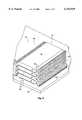
- FIG. 1one embodiment of a multi-chip package 10 of the invention is illustrated.
- the multi-chip package 10is shown with a stack 12 of four primary semiconductor packaged devices 14, also simply called “primary packages” herein, such as are well known in the art.
- Each primary package 14contains at least one semiconductor die having interconnections such as by a lead frame to a plurality of outer leads 16.
- the semiconductor die and lead frameare not visible in the drawing figures, being within the protective layer of e.g. insulative polymer on the exterior of each primary package 14.
- Each primary package 14is shown with major upper and lower surfaces 18 and 20 which are connected by ends 22, 24 and lateral edges 26 and 28. Truncated outer leads 16 are shown extending outwardly from each of lateral edges 26 and 28, respectively.
- the primary packages 14are joined to each other and to a host circuit board 30 by nonconductive adhesive material 32, which may be a tape such as Kapton polyimide, or a flowable adhesive cement.
- Nonconductive adhesive material 32which may be a tape such as Kapton polyimide, or a flowable adhesive cement.
- Circuit board 30is shown with electrically conductive pads 34 for connection to the multi-chip package 10.
- the primary packages 14are electrically joined by a flexible connector 36, details of which are shown in drawing FIGS. 1-8.
- the connector 36comprises a layer 38 of insulative polymeric material such as Kapton polyimide. On one side 42 of the polymeric layer 38 is superposed a series of parallel conductive buses 40. The buses 40 are spaced on the polymeric layer 38 to match the spacing of the outer leads 16. The buses 40 may be metal wire of varied cross-sectional shapes and adhesively joined to the polymeric layer 38.
- FIGS. 2-6Shown in drawing FIGS. 2-6 are five exemplary configurations of buses 40 which may be used in the connector 36. Other shapes may also be used.
- the busesmay be a simple round wire 40A attached with adhesive 44 to side 42 of the polymeric layer 38, as shown in FIG. 2.
- the pitch 48 of the wires 40Ais controlled to equal the spacing or pitch of the outer leads 16.
- Side 54 of the polymeric layer 38is the external surface of the connector 36.
- FIG. 3a semi-round wire 40B is depicted, and drawing FIG. 4 shows a flat wire 40C attached with adhesive 44. As depicted in drawing FIG. 5, a flat wire 40D with side grooves 46 for enhancing the attachment forces of the wire to the polymeric layer 38 with adhesive 44 is shown.
- the bus 40may be attached to the polymeric layer 38 by heating the wire and pressing it into the layer.
- the wire 40Emay have a shape which includes a lock 50 which is embedded in the polymeric layer 38 for firmly attaching the wire to the polymeric layer.
- the wire 40Emay be heated by passing an electric current through the wire.
- the flexibility of the connector 36permits conformation to the rows of outer leads 16 and the lateral edges 26, 28 of the primary packages 14.
- the bending of the connector 36is exaggerated in FIG. 1 for better comprehension.
- Use of the connector 36 of drawing FIG. 1permits formation of a four-package multi-chip package device 10 having an overall height 64 (FIG. 12) of about 6 mm or less.
- the polymeric layer 38 of the connector 36may have a typical thickness 52 (FIG. 2) of about one (1) to about five (5) mils, and is preferably formed of polyimide, although other suitable polymers may be used.
- the buses 40have cross-sectional dimensions such that the impedance and inductance are sufficiently low to enable high quality operation at the specified clock speed and power rating. For example, in a multi-chip device of four primary memory packages, a suitable round aluminum wire 40A provides acceptable conductance and impedance.
- the outer leads 16 of the primary packages 14, as well as the buses 40have a uniform pitch, i.e. spacing.
- the buses 40 of connector 36are attached to the outer leads 16 of the primary packages 14 such that the equivalent outer leads of the packages are attached to the same bus.
- Each bus 40has one end 56 which is attachable to a conductive pad 34 of the host circuit board 30.
- the bus-to-lead and bus-to-pad connectionsmay be made with heat, e.g. a low temperature solder, by pressure, or with application of a conductive adhesive, or by any suitable well known connection methods in the art.
- the connector 36may be formed as a semicontinuous tape 58 with transverse buses 40 attached to the polymeric layer 38, e.g. KaptonTM polyimide.
- the tape 58may be pre-manufactured to provide the desired bus configurations, pitch 48 and tape widths 60 applicable to a manufacturer's product line.
- the tape 58is cut to fit each multi-IC chip package.
- the tapemay be placed on a spool 62 for easy dispensing and use.
- a flex-circuit 58having transverse buses 40 secured to an etched polymeric layer 38 exposing the buses 40 may be used.
- a multi-IC chip package 10is shown with a stack 12 of primary packages 12 as previously described.
- the outer leads 16 of the primary packages 14are truncated to extend only a short distance outward from the packages.
- the connector 36comprises a series of buses 40 formed of a flowable conductive material which sets to a hard but flexible conductor capable of high conductance, low impedance performance.
- the conductive material of the buses 40may be a polymer e.g. epoxy, containing small particles of conductive metal, i.e. silver, gold or aluminum.
- the buses materialmay be a polymer having sufficient conductance and low impedance for high-speed operation.
- Examples of conductive polymersinclude doped polyacetylene, polypyrrole, polythiophene and polyaniline.
- the dopantis selected to provide the desired electrical properties and may be, for example, iodine.
- the materialmay be selected to set upon a change in temperature or by radiation, for example. If necessary, chemical agents for retarding or enhancing the setting speed may be included in the polymer formulation.
- each bus 40is formed by passing conductive polymer 66 with a controlled setting rate in a minute stream 68 from an outlet 74 of a polymer extruder 70.
- the extruderis moved up and/or down in a vertical direction 72 and in a horizontal direction 76 to join the equivalent outer leads 16 of the primary packages 14 with the conductive pads 34 of the host circuit board 30.
- the bus 40is built up to the desired cross-section for optimal device performance.
- a plurality, or even all of the buses 40may be formed simultaneously using a polymer extruder 70 with multiple outlets 74.
- the multi-IC chip packageis adaptable to stacks 12 of primary packages 14 having outer leads 16 on one, two, three or four sides.
- the stack 12may comprise two or more primary packages 14, but typically will comprise about four packages, each with outer leads 16 on one or two sides.
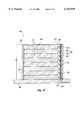
- the multi-IC chip package 80has a stack connector 82, illustrated as comprising a cage 84, for holding by friction an exemplary stack 86 of eight primary packages 14.
- the cage 84is shown to contact a portion or portions of lateral edge 26 of each primary package 14, and closely approach or contact the package ends 22, 24.
- the cage 84partially encloses the primary packages 14 to retain them as a stack.
- the cage 84may be formed of a thin metal sheet, a strong polymeric material, ceramic, or the like.
- the cage 84is most easily formed from a metal sheet, extruded metal, extruded plastic, molded plastic, thermoplastic, etc., typically of five (5) to one- hundred (100), mils thickness 100, which is cut and bent at 90 degrees at each of the four corners 102, 104, 106, and 108, forming the five panels 110, 112, 114, 116 and 118.
- a gap 120 between coplanar panels 116 and 118permits easy removal of primary packages 14 from the cage 84.
- the high heat conductivity of the cage 84results in enhanced heat dissipation from the multi-IC chip package or module 80 during use.
- the cage 84also acts as a heat sink to minimize temperature variations of the primary packages 14.
- a thin "flex PCB” 92is attached by a layer 94 of elastomeric adhesive.
- the thickness 96 of the adhesive layer 94is controlled to provide a desired degree of flexibility.
- Buses 90are formed on the flex PCB 92 with a pitch 48 matching the pitch 49 of the outer leads 16, and are positioned to contact the sets of corresponding outer leads 16 of the primary packages 14 when they are inserted into the cage 84.
- the buses 90may be metal strips attached to the flex PCB 92 by adhesive, not shown, or may be formed by metallization and lithographic bus separation, for example. If desired, the outer leads 16 of the primary packages 14 may be soldered to the buses 90 or connected to the buses 90 using suitable conductive material.
- each of the buses 90is shown as comprising a horizontal portion insulated from the cage 84 by non-conductive adhesive 94.
- the lower end 124may be attached to a conductive pad or lead 34 of the host circuit board 30 by methods well-known in the art, e.g. by surface mounting with solder, bonding with conductive adhesive, and the like.
- the thin flex PCB 92 and elastomeric adhesive layer 94provide resilience by which variations in dimensions of the primary packages 14 and their buses 90 are accommodated.
- the thickness 98 of the flex PCB 92is about one (1) to five (5) mils
- the thickness 96 of the adhesive layeris about three (3) to eight (8) mils, but thicknesses lesser or greater than these values may be used.
- the outer leads 16 of the primary packages 14are bent to flex with compressive forces imposed by the cage 84, flex PCB 92 and elastomeric adhesive layer 94.
- the primary packages 14may be easily inserted and extracted merely by pulling them from the cage 84. Desoldering or other steps of heating, cutting, etc. are not required to remove a primary package 14.
- a small dab(s) of adhesivemay be used to fix the topmost primary package 14 to the cage.
- the adhesivemay be easily removed if necessary to replace a primary package.
- a small node or nodes 122 of polymeric materialmay be formed on one or more cage panels 110, 112, 114, 116 and 118 to provide an additional resistance to removal of any primary package 14.
- the nodesmay be ribs 122 which conform to the shape of primary packages 14 to maintain the entire exemplary stack 86 immobile during use, yet allow easy removal.
- a multi-IC chip package 80 with eight typical primary packages 14 eight-hundred (800) mils in length and four-hundred-fifty (450) mils in widthmay have an overall height of less than about ten (10) mm.
- This embodiment of a multi-IC chip package 80is most aptly applied to primary packages 14 having outer leads 16 along one side only.
- two opposing flex PCB members 92 with buses 90could be attached to opposing inner walls of a cage 84 to accommodate primary packages 14 with outer leads 16 along both opposing lateral edges 26 and 28.
- the cage 84 with attached flex PCB 92 and buses 90is attached to the host circuit board 30 with adhesive and the bus lower ends 124 are soldered or otherwise attached to the conductive pads or leads 34 of the host circuit board 30.
- the primary packages 14are then inserted and pushed downwardly within the cage 84 to form an exemplary stack 86, the outer leads 16 of each primary package compressed slightly during the insertion step.
- the footprints of the multi-IC chip packages 10 and 80are only slightly larger than the footprint of a primary package 14 which is stacked in packages 10 and 80. Thus, the density is considerably greater than the SIMM and DIMM packages currently in use.
- the number of primary packages 14 which may be incorporated in the stackis typically eight or more, but fewer than eight may be used.
- FIG. 13Another embodiment of the multi-IC chip package is illustrated in drawing FIG. 13.
- This multi-IC chip package 130is similar to the package 80 of drawing FIGS. 11 and 12, except that the cage 132 has but three full panels and has no flex PCB or buses.
- the cage 132is rotated relative to cage 84 of package 80 so that the outer leads 16 of the primary packages 14 may be directly attached to conductive pads or elongate leads 34 of the host circuit board 30 without an intervening panel.
- the primary packages 14have their major upper and lower surfaces 18, 20 in a vertical attitude and are stacked horizontally. Thus, the height dimension 134 is the same regardless of the number of primary packages 14 in the stack.
- the two opposed cage wallsare attached to the host circuit board 30, e.g. by adhesive 136 or other means, such as snap pins, not shown in drawing FIG. 13, which are fitted into holes in the host circuit board 30. Alternately, the cage 132 may be soldered to the circuit board 30.
- Small ribs 122may be incorporated into inner walls of the cage 132 to provide resistance to removal of the primary packages 14 from the cage.
- the footprint of the multi-IC chip package 130is only slightly larger than the footprint of a primary package 14 which is stacked in packages 10 and 80. Thus, the density is considerably greater than the SIMM and DIMM packages currently in use.
- the inventionprovides for the use of buses which are relatively short and of enhanced cross-section to produce low impedance at high clock speeds, i.e. up to 800 MHz, and relatively high power ratings.
- the multi-IC chip packagesare easy to produce with high accuracy.
- Primary packages using well-developed technologies and having pretested high reliabilityare used in the stacks.
- the inventionis applicable to high speed memory modules which are to supersede the SIMM and DIMM packages.
- each embodiment of the multi-IC chip package of the inventionhas particular advantages under particular circumstances.
Landscapes
- Engineering & Computer Science (AREA)
- Microelectronics & Electronic Packaging (AREA)
- Power Engineering (AREA)
- Physics & Mathematics (AREA)
- Condensed Matter Physics & Semiconductors (AREA)
- General Physics & Mathematics (AREA)
- Computer Hardware Design (AREA)
- Lead Frames For Integrated Circuits (AREA)
- Structures For Mounting Electric Components On Printed Circuit Boards (AREA)
Abstract
Description
Claims (64)
Priority Applications (12)
| Application Number | Priority Date | Filing Date | Title |
|---|---|---|---|
| US09/138,372US6153929A (en) | 1998-08-21 | 1998-08-21 | Low profile multi-IC package connector |
| US09/349,522US6258623B1 (en) | 1998-08-21 | 1999-07-08 | Low profile multi-IC chip package connector |
| US09/639,358US6225689B1 (en) | 1998-08-21 | 2000-08-14 | Low profile multi-IC chip package connector |
| US09/792,771US6475831B2 (en) | 1998-08-21 | 2001-02-23 | Methods for a low profile multi-IC chip package connector |
| US09/836,067US6362519B2 (en) | 1998-08-21 | 2001-04-17 | Low profile multi-IC chip package connector |
| US10/068,081US6486546B2 (en) | 1998-08-21 | 2002-02-06 | Low profile multi-IC chip package connector |
| US10/200,792US6773955B2 (en) | 1998-08-21 | 2002-07-22 | Low profile multi-IC chip package connector |
| US10/206,175US6686655B2 (en) | 1998-08-21 | 2002-07-25 | Low profile multi-IC chip package connector |
| US10/792,222US20040168316A1 (en) | 1998-08-21 | 2004-03-03 | Low profile multi-IC chip package connector |
| US11/040,967US20050158912A1 (en) | 1998-08-21 | 2005-01-21 | Low profile multi-IC chip package connector |
| US11/479,712US20060252180A1 (en) | 1998-08-21 | 2006-06-30 | Method for a low profile multi-IC chip package connector |
| US11/600,946US20080003712A1 (en) | 1998-08-21 | 2006-11-16 | Methods of making semiconductor fuses |
Applications Claiming Priority (1)
| Application Number | Priority Date | Filing Date | Title |
|---|---|---|---|
| US09/138,372US6153929A (en) | 1998-08-21 | 1998-08-21 | Low profile multi-IC package connector |
Related Child Applications (3)
| Application Number | Title | Priority Date | Filing Date |
|---|---|---|---|
| US09/349,522ContinuationUS6258623B1 (en) | 1998-08-21 | 1999-07-08 | Low profile multi-IC chip package connector |
| US09/349,522DivisionUS6258623B1 (en) | 1998-08-21 | 1999-07-08 | Low profile multi-IC chip package connector |
| US09/639,358ContinuationUS6225689B1 (en) | 1998-08-21 | 2000-08-14 | Low profile multi-IC chip package connector |
Publications (1)
| Publication Number | Publication Date |
|---|---|
| US6153929Atrue US6153929A (en) | 2000-11-28 |
Family
ID=22481724
Family Applications (12)
| Application Number | Title | Priority Date | Filing Date |
|---|---|---|---|
| US09/138,372Expired - LifetimeUS6153929A (en) | 1998-08-21 | 1998-08-21 | Low profile multi-IC package connector |
| US09/349,522Expired - LifetimeUS6258623B1 (en) | 1998-08-21 | 1999-07-08 | Low profile multi-IC chip package connector |
| US09/639,358Expired - LifetimeUS6225689B1 (en) | 1998-08-21 | 2000-08-14 | Low profile multi-IC chip package connector |
| US09/792,771Expired - LifetimeUS6475831B2 (en) | 1998-08-21 | 2001-02-23 | Methods for a low profile multi-IC chip package connector |
| US09/836,067Expired - LifetimeUS6362519B2 (en) | 1998-08-21 | 2001-04-17 | Low profile multi-IC chip package connector |
| US10/068,081Expired - LifetimeUS6486546B2 (en) | 1998-08-21 | 2002-02-06 | Low profile multi-IC chip package connector |
| US10/200,792Expired - LifetimeUS6773955B2 (en) | 1998-08-21 | 2002-07-22 | Low profile multi-IC chip package connector |
| US10/206,175Expired - LifetimeUS6686655B2 (en) | 1998-08-21 | 2002-07-25 | Low profile multi-IC chip package connector |
| US10/792,222AbandonedUS20040168316A1 (en) | 1998-08-21 | 2004-03-03 | Low profile multi-IC chip package connector |
| US11/040,967AbandonedUS20050158912A1 (en) | 1998-08-21 | 2005-01-21 | Low profile multi-IC chip package connector |
| US11/479,712AbandonedUS20060252180A1 (en) | 1998-08-21 | 2006-06-30 | Method for a low profile multi-IC chip package connector |
| US11/600,946AbandonedUS20080003712A1 (en) | 1998-08-21 | 2006-11-16 | Methods of making semiconductor fuses |
Family Applications After (11)
| Application Number | Title | Priority Date | Filing Date |
|---|---|---|---|
| US09/349,522Expired - LifetimeUS6258623B1 (en) | 1998-08-21 | 1999-07-08 | Low profile multi-IC chip package connector |
| US09/639,358Expired - LifetimeUS6225689B1 (en) | 1998-08-21 | 2000-08-14 | Low profile multi-IC chip package connector |
| US09/792,771Expired - LifetimeUS6475831B2 (en) | 1998-08-21 | 2001-02-23 | Methods for a low profile multi-IC chip package connector |
| US09/836,067Expired - LifetimeUS6362519B2 (en) | 1998-08-21 | 2001-04-17 | Low profile multi-IC chip package connector |
| US10/068,081Expired - LifetimeUS6486546B2 (en) | 1998-08-21 | 2002-02-06 | Low profile multi-IC chip package connector |
| US10/200,792Expired - LifetimeUS6773955B2 (en) | 1998-08-21 | 2002-07-22 | Low profile multi-IC chip package connector |
| US10/206,175Expired - LifetimeUS6686655B2 (en) | 1998-08-21 | 2002-07-25 | Low profile multi-IC chip package connector |
| US10/792,222AbandonedUS20040168316A1 (en) | 1998-08-21 | 2004-03-03 | Low profile multi-IC chip package connector |
| US11/040,967AbandonedUS20050158912A1 (en) | 1998-08-21 | 2005-01-21 | Low profile multi-IC chip package connector |
| US11/479,712AbandonedUS20060252180A1 (en) | 1998-08-21 | 2006-06-30 | Method for a low profile multi-IC chip package connector |
| US11/600,946AbandonedUS20080003712A1 (en) | 1998-08-21 | 2006-11-16 | Methods of making semiconductor fuses |
Country Status (1)
| Country | Link |
|---|---|
| US (12) | US6153929A (en) |
Cited By (23)
| Publication number | Priority date | Publication date | Assignee | Title |
|---|---|---|---|---|
| US6300687B1 (en)* | 1998-06-26 | 2001-10-09 | International Business Machines Corporation | Micro-flex technology in semiconductor packages |
| US6329221B1 (en) | 1998-03-09 | 2001-12-11 | Micron Technology, Inc. | Method of forming a stack of packaged memory die and resulting apparatus |
| US20020017709A1 (en)* | 2000-06-07 | 2002-02-14 | Yoshiyuki Yanagisawa | Assembly jig and manufacturing method of multilayer semiconductor device |
| WO2002051224A3 (en)* | 2000-12-21 | 2002-10-03 | Synergestic Computing Systems | Multilayered hybrid electronic module |
| WO2002080309A1 (en)* | 2001-03-30 | 2002-10-10 | L-3 Communications Corporation | High density packaging of electronic components |
| US20030080438A1 (en)* | 2001-10-29 | 2003-05-01 | Mitsubishi Denki Kabushiki Kaisha | Semiconductor module |
| US6618257B1 (en)* | 2001-07-27 | 2003-09-09 | Staktek Group, L.P. | Wide data path stacking system and method |
| US20040036163A1 (en)* | 2002-08-22 | 2004-02-26 | Intel Corporation | Multi-die semiconductor package |
| US6707684B1 (en) | 2001-04-02 | 2004-03-16 | Advanced Micro Devices, Inc. | Method and apparatus for direct connection between two integrated circuits via a connector |
| US6734538B1 (en) | 2001-04-12 | 2004-05-11 | Bae Systems Information & Electronic Systems Integration, Inc. | Article comprising a multi-layer electronic package and method therefor |
| US20040168316A1 (en)* | 1998-08-21 | 2004-09-02 | Moden Walter L. | Low profile multi-IC chip package connector |
| US20050146005A1 (en)* | 2001-07-04 | 2005-07-07 | Matsushita Electric Industrial Co., Ltd. | Semiconductor device and manufacturing method thereof |
| US6919626B2 (en) | 1992-12-11 | 2005-07-19 | Staktek Group L.P. | High density integrated circuit module |
| US7066741B2 (en) | 1999-09-24 | 2006-06-27 | Staktek Group L.P. | Flexible circuit connector for stacked chip module |
| US20060148282A1 (en)* | 2004-12-30 | 2006-07-06 | Nokia Corporation | Electronic component assembly |
| US7888185B2 (en)* | 2006-08-17 | 2011-02-15 | Micron Technology, Inc. | Semiconductor device assemblies and systems including at least one conductive pathway extending around a side of at least one semiconductor device |
| JP2013536587A (en)* | 2010-08-25 | 2013-09-19 | イスパノ・シユイザ | Printed circuit comprising at least one ceramic component |
| US20130277818A1 (en)* | 2011-01-20 | 2013-10-24 | Chi Hock Goh | Chip carrier support systems |
| US8611090B2 (en)* | 2010-09-09 | 2013-12-17 | International Business Machines Corporation | Electronic module with laterally-conducting heat distributor layer |
| US8779585B2 (en) | 2011-08-05 | 2014-07-15 | International Business Machines Corporation | Implementing enhanced thermal conductivity in stacked modules |
| US10952352B2 (en) | 2017-10-27 | 2021-03-16 | Micron Technology, Inc. | Assemblies including heat dispersing elements and related systems and methods |
| US11616010B2 (en)* | 2017-06-30 | 2023-03-28 | Hamilton Sundstrand Corporation | Transistor assemblies |
| JPWO2023135709A1 (en)* | 2022-01-13 | 2023-07-20 |
Families Citing this family (182)
| Publication number | Priority date | Publication date | Assignee | Title |
|---|---|---|---|---|
| US6429528B1 (en)* | 1998-02-27 | 2002-08-06 | Micron Technology, Inc. | Multichip semiconductor package |
| FR2797348B1 (en)* | 1999-08-02 | 2001-10-19 | Cit Alcatel | METHOD FOR OBTAINING A HIGH DENSITY MODULE FROM ELECTRONIC, MODULAR, ENCAPSULATED COMPONENTS AND MODULE THUS OBTAINED |
| US6621155B1 (en)* | 1999-12-23 | 2003-09-16 | Rambus Inc. | Integrated circuit device having stacked dies and impedance balanced transmission lines |
| US6558600B1 (en) | 2000-05-04 | 2003-05-06 | Micron Technology, Inc. | Method for packaging microelectronic substrates |
| US6875640B1 (en)* | 2000-06-08 | 2005-04-05 | Micron Technology, Inc. | Stereolithographic methods for forming a protective layer on a semiconductor device substrate and substrates including protective layers so formed |
| US6589820B1 (en) | 2000-06-16 | 2003-07-08 | Micron Technology, Inc. | Method and apparatus for packaging a microelectronic die |
| US6576494B1 (en)* | 2000-06-28 | 2003-06-10 | Micron Technology, Inc. | Recessed encapsulated microelectronic devices and methods for formation |
| US6560117B2 (en) | 2000-06-28 | 2003-05-06 | Micron Technology, Inc. | Packaged microelectronic die assemblies and methods of manufacture |
| US6552910B1 (en) | 2000-06-28 | 2003-04-22 | Micron Technology, Inc. | Stacked-die assemblies with a plurality of microelectronic devices and methods of manufacture |
| US7298031B1 (en) | 2000-08-09 | 2007-11-20 | Micron Technology, Inc. | Multiple substrate microelectronic devices and methods of manufacture |
| US6607937B1 (en)* | 2000-08-23 | 2003-08-19 | Micron Technology, Inc. | Stacked microelectronic dies and methods for stacking microelectronic dies |
| US6483044B1 (en)* | 2000-08-23 | 2002-11-19 | Micron Technology, Inc. | Interconnecting substrates for electrical coupling of microelectronic components |
| US7183138B2 (en)* | 2000-08-23 | 2007-02-27 | Micron Technology, Inc. | Method and apparatus for decoupling conductive portions of a microelectronic device package |
| US6979595B1 (en) | 2000-08-24 | 2005-12-27 | Micron Technology, Inc. | Packaged microelectronic devices with pressure release elements and methods for manufacturing and using such packaged microelectronic devices |
| US6838760B1 (en)* | 2000-08-28 | 2005-01-04 | Micron Technology, Inc. | Packaged microelectronic devices with interconnecting units |
| SG148819A1 (en) | 2000-09-14 | 2009-01-29 | Semiconductor Energy Lab | Semiconductor device and manufacturing method thereof |
| TW586195B (en)* | 2001-03-20 | 2004-05-01 | I-Ming Chen | Packaging method of semiconductor dies and the product |
| TW546857B (en)* | 2001-07-03 | 2003-08-11 | Semiconductor Energy Lab | Light-emitting device, method of manufacturing a light-emitting device, and electronic equipment |
| US6564979B2 (en) | 2001-07-18 | 2003-05-20 | Micron Technology, Inc. | Method and apparatus for dispensing adhesive on microelectronic substrate supports |
| SG111919A1 (en) | 2001-08-29 | 2005-06-29 | Micron Technology Inc | Packaged microelectronic devices and methods of forming same |
| KR20030018642A (en) | 2001-08-30 | 2003-03-06 | 주식회사 하이닉스반도체 | Stack chip module |
| US6548376B2 (en) | 2001-08-30 | 2003-04-15 | Micron Technology, Inc. | Methods of thinning microelectronic workpieces |
| US20030042615A1 (en) | 2001-08-30 | 2003-03-06 | Tongbi Jiang | Stacked microelectronic devices and methods of fabricating same |
| US6717222B2 (en)* | 2001-10-07 | 2004-04-06 | Guobiao Zhang | Three-dimensional memory |
| US6747348B2 (en)* | 2001-10-16 | 2004-06-08 | Micron Technology, Inc. | Apparatus and method for leadless packaging of semiconductor devices |
| US6576992B1 (en)* | 2001-10-26 | 2003-06-10 | Staktek Group L.P. | Chip scale stacking system and method |
| US6956284B2 (en) | 2001-10-26 | 2005-10-18 | Staktek Group L.P. | Integrated circuit stacking system and method |
| US7656678B2 (en) | 2001-10-26 | 2010-02-02 | Entorian Technologies, Lp | Stacked module systems |
| EP1317168A1 (en)* | 2001-11-29 | 2003-06-04 | Thomson Licensing S.A. | Data bus connection for memory device |
| US6870276B1 (en)* | 2001-12-26 | 2005-03-22 | Micron Technology, Inc. | Apparatus for supporting microelectronic substrates |
| US6750547B2 (en)* | 2001-12-26 | 2004-06-15 | Micron Technology, Inc. | Multi-substrate microelectronic packages and methods for manufacture |
| US6896760B1 (en)* | 2002-01-16 | 2005-05-24 | Micron Technology, Inc. | Fabrication of stacked microelectronic devices |
| US6690088B2 (en)* | 2002-01-31 | 2004-02-10 | Macintyre Donald M. | Integrated circuit package stacking structure |
| US6635970B2 (en)* | 2002-02-06 | 2003-10-21 | International Business Machines Corporation | Power distribution design method for stacked flip-chip packages |
| US6622380B1 (en) | 2002-02-12 | 2003-09-23 | Micron Technology, Inc. | Methods for manufacturing microelectronic devices and methods for mounting microelectronic packages to circuit boards |
| US7198693B1 (en) | 2002-02-20 | 2007-04-03 | Micron Technology, Inc. | Microelectronic device having a plurality of stacked dies and methods for manufacturing such microelectronic assemblies |
| US7109588B2 (en) | 2002-04-04 | 2006-09-19 | Micron Technology, Inc. | Method and apparatus for attaching microelectronic substrates and support members |
| US6806559B2 (en)* | 2002-04-22 | 2004-10-19 | Irvine Sensors Corporation | Method and apparatus for connecting vertically stacked integrated circuit chips |
| US7777321B2 (en) | 2002-04-22 | 2010-08-17 | Gann Keith D | Stacked microelectronic layer and module with three-axis channel T-connects |
| TWI232560B (en)* | 2002-04-23 | 2005-05-11 | Sanyo Electric Co | Semiconductor device and its manufacture |
| US6826739B2 (en)* | 2002-05-13 | 2004-11-30 | Agilent Technologies, Inc. | System and method for placing substrate contacts in a datapath stack in an integrated circuit design |
| TWI229435B (en) | 2002-06-18 | 2005-03-11 | Sanyo Electric Co | Manufacture of semiconductor device |
| US6903001B2 (en)* | 2002-07-18 | 2005-06-07 | Micron Technology Inc. | Techniques to create low K ILD for BEOL |
| SG120879A1 (en)* | 2002-08-08 | 2006-04-26 | Micron Technology Inc | Packaged microelectronic components |
| SG127684A1 (en)* | 2002-08-19 | 2006-12-29 | Micron Technology Inc | Packaged microelectronic component assemblies |
| US6740546B2 (en)* | 2002-08-21 | 2004-05-25 | Micron Technology, Inc. | Packaged microelectronic devices and methods for assembling microelectronic devices |
| US6845901B2 (en)* | 2002-08-22 | 2005-01-25 | Micron Technology, Inc. | Apparatus and method for depositing and reflowing solder paste on a microelectronic workpiece |
| US6891248B2 (en)* | 2002-08-23 | 2005-05-10 | Micron Technology, Inc. | Semiconductor component with on board capacitor |
| TWI227550B (en) | 2002-10-30 | 2005-02-01 | Sanyo Electric Co | Semiconductor device manufacturing method |
| SG114585A1 (en)* | 2002-11-22 | 2005-09-28 | Micron Technology Inc | Packaged microelectronic component assemblies |
| US20040112935A1 (en)* | 2002-12-16 | 2004-06-17 | Visteon Global Technologies, Inc. | Integrated flex substrate metallurgical bonding |
| JP4554152B2 (en)* | 2002-12-19 | 2010-09-29 | 株式会社半導体エネルギー研究所 | Manufacturing method of semiconductor chip |
| JP4101643B2 (en)* | 2002-12-26 | 2008-06-18 | 株式会社半導体エネルギー研究所 | Method for manufacturing semiconductor device |
| US7132734B2 (en)* | 2003-01-06 | 2006-11-07 | Micron Technology, Inc. | Microelectronic component assemblies and microelectronic component lead frame structures |
| US7436050B2 (en) | 2003-01-22 | 2008-10-14 | Semiconductor Energy Laboratory Co., Ltd. | Semiconductor device having a flexible printed circuit |
| SE0300160D0 (en)* | 2003-01-23 | 2003-01-23 | Siemens Elema Ab | Apparatus for and Method of Mintoring and Gas Supply |
| US6879050B2 (en)* | 2003-02-11 | 2005-04-12 | Micron Technology, Inc. | Packaged microelectronic devices and methods for packaging microelectronic devices |
| JP2004247373A (en) | 2003-02-12 | 2004-09-02 | Semiconductor Energy Lab Co Ltd | Semiconductor device |
| SG143931A1 (en) | 2003-03-04 | 2008-07-29 | Micron Technology Inc | Microelectronic component assemblies employing lead frames having reduced-thickness inner lengths |
| US7183485B2 (en)* | 2003-03-11 | 2007-02-27 | Micron Technology, Inc. | Microelectronic component assemblies having lead frames adapted to reduce package bow |
| SG137651A1 (en)* | 2003-03-14 | 2007-12-28 | Micron Technology Inc | Microelectronic devices and methods for packaging microelectronic devices |
| JP4526771B2 (en) | 2003-03-14 | 2010-08-18 | 株式会社半導体エネルギー研究所 | Method for manufacturing semiconductor device |
| US6917090B2 (en)* | 2003-04-07 | 2005-07-12 | Micron Technology, Inc. | Chip scale image sensor package |
| SG143932A1 (en)* | 2003-05-30 | 2008-07-29 | Micron Technology Inc | Packaged microelectronic devices and methods of packaging microelectronic devices |
| US20040264148A1 (en)* | 2003-06-27 | 2004-12-30 | Burdick William Edward | Method and system for fan fold packaging |
| JP4401181B2 (en) | 2003-08-06 | 2010-01-20 | 三洋電機株式会社 | Semiconductor device and manufacturing method thereof |
| US7071421B2 (en) | 2003-08-29 | 2006-07-04 | Micron Technology, Inc. | Stacked microfeature devices and associated methods |
| US7368810B2 (en)* | 2003-08-29 | 2008-05-06 | Micron Technology, Inc. | Invertible microfeature device packages |
| US6924655B2 (en)* | 2003-09-03 | 2005-08-02 | Micron Technology, Inc. | Probe card for use with microelectronic components, and methods for making same |
| US7091124B2 (en) | 2003-11-13 | 2006-08-15 | Micron Technology, Inc. | Methods for forming vias in microelectronic devices, and methods for packaging microelectronic devices |
| US20050104171A1 (en)* | 2003-11-13 | 2005-05-19 | Benson Peter A. | Microelectronic devices having conductive complementary structures and methods of manufacturing microelectronic devices having conductive complementary structures |
| US8084866B2 (en)* | 2003-12-10 | 2011-12-27 | Micron Technology, Inc. | Microelectronic devices and methods for filling vias in microelectronic devices |
| US6998703B2 (en)* | 2003-12-04 | 2006-02-14 | Palo Alto Research Center Inc. | Thin package for stacking integrated circuits |
| JP4205613B2 (en)* | 2004-03-01 | 2009-01-07 | エルピーダメモリ株式会社 | Semiconductor device |
| US7245021B2 (en)* | 2004-04-13 | 2007-07-17 | Vertical Circuits, Inc. | Micropede stacked die component assembly |
| US7215018B2 (en)* | 2004-04-13 | 2007-05-08 | Vertical Circuits, Inc. | Stacked die BGA or LGA component assembly |
| US7705432B2 (en) | 2004-04-13 | 2010-04-27 | Vertical Circuits, Inc. | Three dimensional six surface conformal die coating |
| SG145547A1 (en)* | 2004-07-23 | 2008-09-29 | Micron Technology Inc | Microelectronic component assemblies with recessed wire bonds and methods of making same |
| US7632747B2 (en)* | 2004-08-19 | 2009-12-15 | Micron Technology, Inc. | Conductive structures for microfeature devices and methods for fabricating microfeature devices |
| US7602618B2 (en)* | 2004-08-25 | 2009-10-13 | Micron Technology, Inc. | Methods and apparatuses for transferring heat from stacked microfeature devices |
| US20060043534A1 (en)* | 2004-08-26 | 2006-03-02 | Kirby Kyle K | Microfeature dies with porous regions, and associated methods and systems |
| US7095122B2 (en)* | 2004-09-01 | 2006-08-22 | Micron Technology, Inc. | Reduced-dimension microelectronic component assemblies with wire bonds and methods of making same |
| US7422935B2 (en)* | 2004-09-24 | 2008-09-09 | Semiconductor Energy Laboratory Co., Ltd. | Method for manufacturing semiconductor device, and semiconductor device and electronic device |
| US20060071316A1 (en)* | 2004-09-24 | 2006-04-06 | Emory Garth | Three-dimensional stack manufacture for integrated circuit devices and method of manufacture |
| CN100347856C (en)* | 2004-09-27 | 2007-11-07 | 赵建铭 | Package with multiple chips packaged and packaging method thereof |
| CN101138089B (en)* | 2005-01-31 | 2011-02-09 | 斯班逊有限公司 | Stacked semiconductor device and method for manufacturing stacked semiconductor device |
| US8278751B2 (en) | 2005-02-08 | 2012-10-02 | Micron Technology, Inc. | Methods of adhering microfeature workpieces, including a chip, to a support member |
| US7242091B2 (en)* | 2005-03-02 | 2007-07-10 | Stats Chippac Ltd. | Stacked semiconductor packages and method therefor |
| JP4311376B2 (en) | 2005-06-08 | 2009-08-12 | セイコーエプソン株式会社 | Semiconductor device, semiconductor device manufacturing method, electronic component, circuit board, and electronic apparatus |
| SG130055A1 (en)* | 2005-08-19 | 2007-03-20 | Micron Technology Inc | Microelectronic devices, stacked microelectronic devices, and methods for manufacturing microelectronic devices |
| SG130061A1 (en)* | 2005-08-24 | 2007-03-20 | Micron Technology Inc | Microelectronic devices and microelectronic support devices, and associated assemblies and methods |
| SG130066A1 (en)* | 2005-08-26 | 2007-03-20 | Micron Technology Inc | Microelectronic device packages, stacked microelectronic device packages, and methods for manufacturing microelectronic devices |
| US7807505B2 (en)* | 2005-08-30 | 2010-10-05 | Micron Technology, Inc. | Methods for wafer-level packaging of microfeature devices and microfeature devices formed using such methods |
| US7745944B2 (en) | 2005-08-31 | 2010-06-29 | Micron Technology, Inc. | Microelectronic devices having intermediate contacts for connection to interposer substrates, and associated methods of packaging microelectronic devices with intermediate contacts |
| US7485969B2 (en)* | 2005-09-01 | 2009-02-03 | Micron Technology, Inc. | Stacked microelectronic devices and methods for manufacturing microelectronic devices |
| US20070045807A1 (en)* | 2005-09-01 | 2007-03-01 | Micron Technology, Inc. | Microelectronic devices and methods for manufacturing microelectronic devices |
| US7622377B2 (en) | 2005-09-01 | 2009-11-24 | Micron Technology, Inc. | Microfeature workpiece substrates having through-substrate vias, and associated methods of formation |
| US20070148820A1 (en)* | 2005-12-22 | 2007-06-28 | Micron Technology, Inc. | Microelectronic devices and methods for manufacturing microelectronic devices |
| TWI324800B (en) | 2005-12-28 | 2010-05-11 | Sanyo Electric Co | Method for manufacturing semiconductor device |
| SG133445A1 (en)* | 2005-12-29 | 2007-07-30 | Micron Technology Inc | Methods for packaging microelectronic devices and microelectronic devices formed using such methods |
| TWI293499B (en)* | 2006-01-25 | 2008-02-11 | Advanced Semiconductor Eng | Three dimensional package and method of making the same |
| TWI287273B (en)* | 2006-01-25 | 2007-09-21 | Advanced Semiconductor Eng | Three dimensional package and method of making the same |
| SG135074A1 (en) | 2006-02-28 | 2007-09-28 | Micron Technology Inc | Microelectronic devices, stacked microelectronic devices, and methods for manufacturing such devices |
| SG135979A1 (en)* | 2006-03-08 | 2007-10-29 | Micron Technology Inc | Microelectronic device assemblies including assemblies with recurved leadframes, and associated methods |
| SG136009A1 (en) | 2006-03-29 | 2007-10-29 | Micron Technology Inc | Packaged microelectronic devices recessed in support member cavities, and associated methods |
| US7910385B2 (en)* | 2006-05-12 | 2011-03-22 | Micron Technology, Inc. | Method of fabricating microelectronic devices |
| SG138501A1 (en)* | 2006-07-05 | 2008-01-28 | Micron Technology Inc | Lead frames, microelectronic devices with lead frames, and methods for manufacturing lead frames and microelectronic devices with lead frames |
| SG139573A1 (en)* | 2006-07-17 | 2008-02-29 | Micron Technology Inc | Microelectronic packages with leadframes, including leadframes configured for stacked die packages, and associated systems and methods |
| US7868440B2 (en) | 2006-08-25 | 2011-01-11 | Micron Technology, Inc. | Packaged microdevices and methods for manufacturing packaged microdevices |
| US7829438B2 (en) | 2006-10-10 | 2010-11-09 | Tessera, Inc. | Edge connect wafer level stacking |
| US8513789B2 (en) | 2006-10-10 | 2013-08-20 | Tessera, Inc. | Edge connect wafer level stacking with leads extending along edges |
| US7901989B2 (en) | 2006-10-10 | 2011-03-08 | Tessera, Inc. | Reconstituted wafer level stacking |
| JP2008108890A (en)* | 2006-10-25 | 2008-05-08 | Three M Innovative Properties Co | Adhesion method for circuit board and adhesion structure body |
| US7476563B2 (en) | 2006-11-17 | 2009-01-13 | Freescale Semiconductor, Inc. | Method of packaging a device using a dielectric layer |
| US7807511B2 (en)* | 2006-11-17 | 2010-10-05 | Freescale Semiconductor, Inc. | Method of packaging a device having a multi-contact elastomer connector contact area and device thereof |
| US7588951B2 (en)* | 2006-11-17 | 2009-09-15 | Freescale Semiconductor, Inc. | Method of packaging a semiconductor device and a prefabricated connector |
| US7696016B2 (en)* | 2006-11-17 | 2010-04-13 | Freescale Semiconductor, Inc. | Method of packaging a device having a tangible element and device thereof |
| CN100505248C (en)* | 2006-11-27 | 2009-06-24 | 南茂科技股份有限公司 | Stacked chip package with heat dissipation structure |
| SG143098A1 (en) | 2006-12-04 | 2008-06-27 | Micron Technology Inc | Packaged microelectronic devices and methods for manufacturing packaged microelectronic devices |
| US7656031B2 (en)* | 2007-02-05 | 2010-02-02 | Bridge Semiconductor Corporation | Stackable semiconductor package having metal pin within through hole of package |
| US7833456B2 (en) | 2007-02-23 | 2010-11-16 | Micron Technology, Inc. | Systems and methods for compressing an encapsulant adjacent a semiconductor workpiece |
| US7750449B2 (en)* | 2007-03-13 | 2010-07-06 | Micron Technology, Inc. | Packaged semiconductor components having substantially rigid support members and methods of packaging semiconductor components |
| US8723332B2 (en)* | 2007-06-11 | 2014-05-13 | Invensas Corporation | Electrically interconnected stacked die assemblies |
| TW200917391A (en)* | 2007-06-20 | 2009-04-16 | Vertical Circuits Inc | Three-dimensional circuitry formed on integrated circuit device using two-dimensional fabrication |
| SG149726A1 (en) | 2007-07-24 | 2009-02-27 | Micron Technology Inc | Microelectronic die packages with metal leads, including metal leads for stacked die packages, and associated systems and methods |
| SG149725A1 (en)* | 2007-07-24 | 2009-02-27 | Micron Technology Inc | Thin semiconductor die packages and associated systems and methods |
| SG149724A1 (en)* | 2007-07-24 | 2009-02-27 | Micron Technology Inc | Semicoductor dies with recesses, associated leadframes, and associated systems and methods |
| JP5572089B2 (en) | 2007-07-27 | 2014-08-13 | テッセラ,インコーポレイテッド | Reconfigured wafer stack packaging with pad extension after application |
| US8551815B2 (en) | 2007-08-03 | 2013-10-08 | Tessera, Inc. | Stack packages using reconstituted wafers |
| US8043895B2 (en)* | 2007-08-09 | 2011-10-25 | Tessera, Inc. | Method of fabricating stacked assembly including plurality of stacked microelectronic elements |
| SG150396A1 (en)* | 2007-08-16 | 2009-03-30 | Micron Technology Inc | Microelectronic die packages with leadframes, including leadframe-based interposer for stacked die packages, and associated systems and methods |
| WO2009035849A2 (en) | 2007-09-10 | 2009-03-19 | Vertical Circuits, Inc. | Semiconductor die mount by conformal die coating |
| US7838978B2 (en)* | 2007-09-19 | 2010-11-23 | Infineon Technologies Ag | Semiconductor device |
| JP4588060B2 (en)* | 2007-09-19 | 2010-11-24 | スパンション エルエルシー | Semiconductor device and manufacturing method thereof |
| TW200931634A (en)* | 2008-01-10 | 2009-07-16 | Abounion Technology Corp | Multi-channel stacked semiconductor device and method for fabricating the same, and stacking substrate applied to the semiconductor device |
| US7843046B2 (en)* | 2008-02-19 | 2010-11-30 | Vertical Circuits, Inc. | Flat leadless packages and stacked leadless package assemblies |
| CN101999167B (en)* | 2008-03-12 | 2013-07-17 | 伊文萨思公司 | Support mounted electrically interconnected die assembly |
| US9153517B2 (en) | 2008-05-20 | 2015-10-06 | Invensas Corporation | Electrical connector between die pad and z-interconnect for stacked die assemblies |
| US7863159B2 (en)* | 2008-06-19 | 2011-01-04 | Vertical Circuits, Inc. | Semiconductor die separation method |
| JP5639052B2 (en)* | 2008-06-16 | 2014-12-10 | テッセラ,インコーポレイテッド | Edge stacking at wafer level |
| US7906372B2 (en)* | 2008-07-09 | 2011-03-15 | Avago Technologies Fiber Ip (Singapore) Pte. Ltd | Lens support and wirebond protector |
| US7872332B2 (en)* | 2008-09-11 | 2011-01-18 | Micron Technology, Inc. | Interconnect structures for stacked dies, including penetrating structures for through-silicon vias, and associated systems and methods |
| US8357013B2 (en)* | 2009-01-22 | 2013-01-22 | Hirose Electric Co., Ltd. | Reducing far-end crosstalk in electrical connectors |
| JP4833307B2 (en)* | 2009-02-24 | 2011-12-07 | インターナショナル・ビジネス・マシーンズ・コーポレーション | Semiconductor module, terminal plate, method for manufacturing terminal plate, and method for manufacturing semiconductor module |
| WO2010104610A2 (en)* | 2009-03-13 | 2010-09-16 | Tessera Technologies Hungary Kft. | Stacked microelectronic assemblies having vias extending through bond pads |
| WO2010151578A2 (en)* | 2009-06-26 | 2010-12-29 | Vertical Circuits, Inc. | Electrical interconnect for die stacked in zig-zag configuration |
| WO2011056668A2 (en) | 2009-10-27 | 2011-05-12 | Vertical Circuits, Inc. | Selective die electrical insulation additive process |
| TWI544604B (en) | 2009-11-04 | 2016-08-01 | 英維瑟斯公司 | Stacked die assembly having reduced stress electrical interconnects |
| JP5742242B2 (en)* | 2011-01-21 | 2015-07-01 | セイコーエプソン株式会社 | Substrate connection method and semiconductor device manufacturing method |
| US8587088B2 (en)* | 2011-02-17 | 2013-11-19 | Apple Inc. | Side-mounted controller and methods for making the same |
| KR20120135626A (en)* | 2011-06-07 | 2012-12-17 | 삼성전자주식회사 | Method for manufacturing semiconductor chip package |
| US9086553B2 (en) | 2011-06-27 | 2015-07-21 | Avago Technologies General Ip (Singapore) Pte. Ltd. | Optical communications device having electrical bond pads that are protected by a protective coating, and a method for applying the protective coating |
| US8516426B2 (en) | 2011-08-25 | 2013-08-20 | International Business Machines Corporation | Vertical power budgeting and shifting for three-dimensional integration |
| US8519735B2 (en) | 2011-08-25 | 2013-08-27 | International Business Machines Corporation | Programming the behavior of individual chips or strata in a 3D stack of integrated circuits |
| US8381156B1 (en) | 2011-08-25 | 2013-02-19 | International Business Machines Corporation | 3D inter-stratum connectivity robustness |
| US8525569B2 (en) | 2011-08-25 | 2013-09-03 | International Business Machines Corporation | Synchronizing global clocks in 3D stacks of integrated circuits by shorting the clock network |
| US8476771B2 (en) | 2011-08-25 | 2013-07-02 | International Business Machines Corporation | Configuration of connections in a 3D stack of integrated circuits |
| US8576000B2 (en) | 2011-08-25 | 2013-11-05 | International Business Machines Corporation | 3D chip stack skew reduction with resonant clock and inductive coupling |
| US8587357B2 (en) | 2011-08-25 | 2013-11-19 | International Business Machines Corporation | AC supply noise reduction in a 3D stack with voltage sensing and clock shifting |
| US8476953B2 (en) | 2011-08-25 | 2013-07-02 | International Business Machines Corporation | 3D integrated circuit stack-wide synchronization circuit |
| US8796822B2 (en) | 2011-10-07 | 2014-08-05 | Freescale Semiconductor, Inc. | Stacked semiconductor devices |
| US9076664B2 (en)* | 2011-10-07 | 2015-07-07 | Freescale Semiconductor, Inc. | Stacked semiconductor die with continuous conductive vias |
| US9390772B2 (en)* | 2012-05-22 | 2016-07-12 | Samsung Electronics Co., Ltd. | Semiconductor device including option pads for determining an operating structure thereof, and a system having the same |
| US9826640B2 (en) | 2013-06-26 | 2017-11-21 | E Ink Holdings Inc. | Electronic apparatus |
| TWI507772B (en)* | 2013-06-26 | 2015-11-11 | E Ink Holdings Inc | Electronic apparatus |
| JP2016535445A (en)* | 2013-10-29 | 2016-11-10 | ケメット エレクトロニクス コーポレーション | Ceramic capacitor with improved lead design |
| US9082757B2 (en)* | 2013-10-31 | 2015-07-14 | Freescale Semiconductor, Inc. | Stacked semiconductor devices |
| US9257419B2 (en)* | 2014-03-17 | 2016-02-09 | Freescale Semiconductor Inc. | Leadframe-based system-in-packages having sidewall-mounted surface mount devices and methods for the production thereof |
| KR102222484B1 (en) | 2014-05-27 | 2021-03-04 | 에스케이하이닉스 주식회사 | Flexible stack package with wing portion |
| US9691746B2 (en) | 2014-07-14 | 2017-06-27 | Micron Technology, Inc. | Methods of manufacturing stacked semiconductor die assemblies with high efficiency thermal paths |
| US9337119B2 (en)* | 2014-07-14 | 2016-05-10 | Micron Technology, Inc. | Stacked semiconductor die assemblies with high efficiency thermal paths and associated systems |
| US10002653B2 (en) | 2014-10-28 | 2018-06-19 | Nxp Usa, Inc. | Die stack address bus having a programmable width |
| US9490195B1 (en) | 2015-07-17 | 2016-11-08 | Invensas Corporation | Wafer-level flipped die stacks with leadframes or metal foil interconnects |
| US9825002B2 (en) | 2015-07-17 | 2017-11-21 | Invensas Corporation | Flipped die stack |
| US9871019B2 (en) | 2015-07-17 | 2018-01-16 | Invensas Corporation | Flipped die stack assemblies with leadframe interconnects |
| US9508691B1 (en) | 2015-12-16 | 2016-11-29 | Invensas Corporation | Flipped die stacks with multiple rows of leadframe interconnects |
| US10566310B2 (en) | 2016-04-11 | 2020-02-18 | Invensas Corporation | Microelectronic packages having stacked die and wire bond interconnects |
| US9595511B1 (en) | 2016-05-12 | 2017-03-14 | Invensas Corporation | Microelectronic packages and assemblies with improved flyby signaling operation |
| US9728524B1 (en) | 2016-06-30 | 2017-08-08 | Invensas Corporation | Enhanced density assembly having microelectronic packages mounted at substantial angle to board |
| CN108010906A (en)* | 2017-11-29 | 2018-05-08 | 上海先方半导体有限公司 | A kind of package structure of semiconductor device and method for packing |
| US10595439B2 (en)* | 2018-06-25 | 2020-03-17 | Intel Corporation | Movable heatsink utilizing flexible heat pipes |
| CN110265292B (en)* | 2019-04-26 | 2021-07-27 | 芯盟科技有限公司 | Three-dimensional memory and manufacturing method |
Citations (35)
| Publication number | Priority date | Publication date | Assignee | Title |
|---|---|---|---|---|
| US4992849A (en)* | 1989-02-15 | 1991-02-12 | Micron Technology, Inc. | Directly bonded board multiple integrated circuit module |
| US4992850A (en)* | 1989-02-15 | 1991-02-12 | Micron Technology, Inc. | Directly bonded simm module |
| US4996587A (en)* | 1989-04-10 | 1991-02-26 | International Business Machines Corporation | Integrated semiconductor chip package |
| US5107328A (en)* | 1991-02-13 | 1992-04-21 | Micron Technology, Inc. | Packaging means for a semiconductor die having particular shelf structure |
| US5137836A (en)* | 1991-05-23 | 1992-08-11 | Atmel Corporation | Method of manufacturing a repairable multi-chip module |
| US5155067A (en)* | 1991-03-26 | 1992-10-13 | Micron Technology, Inc. | Packaging for a semiconductor die |
| US5239198A (en)* | 1989-09-06 | 1993-08-24 | Motorola, Inc. | Overmolded semiconductor device having solder ball and edge lead connective structure |
| US5239747A (en)* | 1991-09-18 | 1993-08-31 | Sgs-Thomson Microelectronics, Inc. | Method of forming integrated circuit devices |
| US5255156A (en)* | 1989-02-22 | 1993-10-19 | The Boeing Company | Bonding pad interconnection on a multiple chip module having minimum channel width |
| US5281852A (en)* | 1991-12-10 | 1994-01-25 | Normington Peter J C | Semiconductor device including stacked die |
| US5323060A (en)* | 1993-06-02 | 1994-06-21 | Micron Semiconductor, Inc. | Multichip module having a stacked chip arrangement |
| US5343366A (en)* | 1992-06-24 | 1994-08-30 | International Business Machines Corporation | Packages for stacked integrated circuit chip cubes |
| US5343075A (en)* | 1991-06-29 | 1994-08-30 | Sony Corporation | Composite stacked semiconductor device with contact plates |
| US5378981A (en)* | 1993-02-02 | 1995-01-03 | Motorola, Inc. | Method for testing a semiconductor device on a universal test circuit substrate |
| US5420751A (en)* | 1990-08-01 | 1995-05-30 | Staktek Corporation | Ultra high density modular integrated circuit package |
| US5424652A (en)* | 1992-06-10 | 1995-06-13 | Micron Technology, Inc. | Method and apparatus for testing an unpackaged semiconductor die |
| US5448165A (en)* | 1993-01-08 | 1995-09-05 | Integrated Device Technology, Inc. | Electrically tested and burned-in semiconductor die and method for producing same |
| US5461544A (en)* | 1993-03-05 | 1995-10-24 | Sgs-Thomson Microelectronics, Inc. | Structure and method for connecting leads from multiple chips |
| US5465470A (en)* | 1994-08-31 | 1995-11-14 | Lsi Logic Corporation | Fixture for attaching multiple lids to multi-chip module (MCM) integrated circuit |
| US5468655A (en)* | 1994-10-31 | 1995-11-21 | Motorola, Inc. | Method for forming a temporary attachment between a semiconductor die and a substrate using a metal paste comprising spherical modules |
| US5475317A (en)* | 1993-12-23 | 1995-12-12 | Epi Technologies, Inc. | Singulated bare die tester and method of performing forced temperature electrical tests and burn-in |
| US5480840A (en)* | 1992-07-14 | 1996-01-02 | At&T Global Information Solutions Company | Multi-chip module with multiple compartments |
| US5484959A (en)* | 1992-12-11 | 1996-01-16 | Staktek Corporation | High density lead-on-package fabrication method and apparatus |
| US5495398A (en)* | 1992-05-22 | 1996-02-27 | National Semiconductor Corporation | Stacked multi-chip modules and method of manufacturing |
| US5514907A (en)* | 1995-03-21 | 1996-05-07 | Simple Technology Incorporated | Apparatus for stacking semiconductor chips |
| US5535101A (en)* | 1992-11-03 | 1996-07-09 | Motorola, Inc. | Leadless integrated circuit package |
| US5592019A (en)* | 1994-04-19 | 1997-01-07 | Mitsubishi Denki Kabushiki Kaisha | Semiconductor device and module |
| US5600183A (en)* | 1994-11-15 | 1997-02-04 | Hughes Electronics | Multi-layer film adhesive for electrically isolating and grounding an integrated circuit chip to a printed circuit substrate |
| US5602420A (en)* | 1992-09-07 | 1997-02-11 | Hitachi, Ltd. | Stacked high mounting density semiconductor devices |
| US5604377A (en)* | 1995-10-10 | 1997-02-18 | International Business Machines Corp. | Semiconductor chip high density packaging |
| US5625221A (en)* | 1994-03-03 | 1997-04-29 | Samsung Electronics Co., Ltd. | Semiconductor assembly for a three-dimensional integrated circuit package |
| US5637912A (en)* | 1994-08-22 | 1997-06-10 | International Business Machines Corporation | Three-dimensional monolithic electronic module having stacked planar arrays of integrated circuit chips |
| US5657537A (en)* | 1995-05-30 | 1997-08-19 | General Electric Company | Method for fabricating a stack of two dimensional circuit modules |
| US5818107A (en)* | 1997-01-17 | 1998-10-06 | International Business Machines Corporation | Chip stacking by edge metallization |
| US5835988A (en)* | 1996-03-27 | 1998-11-10 | Mitsubishi Denki Kabushiki Kaisha | Packed semiconductor device with wrap around external leads |
Family Cites Families (20)
| Publication number | Priority date | Publication date | Assignee | Title |
|---|---|---|---|---|
| US36916A (en)* | 1862-11-11 | Improvement in coupling thills to axles | ||
| US5446620A (en)* | 1990-08-01 | 1995-08-29 | Staktek Corporation | Ultra high density integrated circuit packages |
| JPH04243173A (en) | 1991-01-17 | 1992-08-31 | Nec Corp | electrostrictive effect element |
| JPH0661404A (en) | 1992-08-10 | 1994-03-04 | Nec Corp | Semiconductor device |
| US6205654B1 (en)* | 1992-12-11 | 2001-03-27 | Staktek Group L.P. | Method of manufacturing a surface mount package |
| US5455740A (en)* | 1994-03-07 | 1995-10-03 | Staktek Corporation | Bus communication system for stacked high density integrated circuit packages |
| KR0134648B1 (en)* | 1994-06-09 | 1998-04-20 | 김광호 | Low Noise Multilayer Chip Package |
| US5891761A (en)* | 1994-06-23 | 1999-04-06 | Cubic Memory, Inc. | Method for forming vertical interconnect process for silicon segments with thermally conductive epoxy preform |
| KR100209782B1 (en)* | 1994-08-30 | 1999-07-15 | 가나이 쓰도무 | Semiconductor device |
| US5648684A (en)* | 1995-07-26 | 1997-07-15 | International Business Machines Corporation | Endcap chip with conductive, monolithic L-connect for multichip stack |
| US5778522A (en)* | 1996-05-20 | 1998-07-14 | Staktek Corporation | Method of manufacturing a high density integrated circuit module with complex electrical interconnect rails having electrical interconnect strain relief |
| US5933712A (en)* | 1997-03-19 | 1999-08-03 | The Regents Of The University Of California | Attachment method for stacked integrated circuit (IC) chips |
| JP3011233B2 (en)* | 1997-05-02 | 2000-02-21 | 日本電気株式会社 | Semiconductor package and its semiconductor mounting structure |
| CA2218307C (en)* | 1997-10-10 | 2006-01-03 | Gennum Corporation | Three dimensional packaging configuration for multi-chip module assembly |
| US5995378A (en)* | 1997-12-31 | 1999-11-30 | Micron Technology, Inc. | Semiconductor device socket, assembly and methods |
| KR100260997B1 (en) | 1998-04-08 | 2000-07-01 | 마이클 디. 오브라이언 | Semiconductor package |
| US5990566A (en)* | 1998-05-20 | 1999-11-23 | Micron Technology, Inc. | High density semiconductor package |
| US6297548B1 (en) | 1998-06-30 | 2001-10-02 | Micron Technology, Inc. | Stackable ceramic FBGA for high thermal applications |
| US6153929A (en)* | 1998-08-21 | 2000-11-28 | Micron Technology, Inc. | Low profile multi-IC package connector |
| US6326687B1 (en)* | 1998-09-01 | 2001-12-04 | Micron Technology, Inc. | IC package with dual heat spreaders |
- 1998
- 1998-08-21USUS09/138,372patent/US6153929A/ennot_activeExpired - Lifetime
- 1999
- 1999-07-08USUS09/349,522patent/US6258623B1/ennot_activeExpired - Lifetime
- 2000
- 2000-08-14USUS09/639,358patent/US6225689B1/ennot_activeExpired - Lifetime
- 2001
- 2001-02-23USUS09/792,771patent/US6475831B2/ennot_activeExpired - Lifetime
- 2001-04-17USUS09/836,067patent/US6362519B2/ennot_activeExpired - Lifetime
- 2002
- 2002-02-06USUS10/068,081patent/US6486546B2/ennot_activeExpired - Lifetime
- 2002-07-22USUS10/200,792patent/US6773955B2/ennot_activeExpired - Lifetime
- 2002-07-25USUS10/206,175patent/US6686655B2/ennot_activeExpired - Lifetime
- 2004
- 2004-03-03USUS10/792,222patent/US20040168316A1/ennot_activeAbandoned
- 2005
- 2005-01-21USUS11/040,967patent/US20050158912A1/ennot_activeAbandoned
- 2006
- 2006-06-30USUS11/479,712patent/US20060252180A1/ennot_activeAbandoned
- 2006-11-16USUS11/600,946patent/US20080003712A1/ennot_activeAbandoned
Patent Citations (35)
| Publication number | Priority date | Publication date | Assignee | Title |
|---|---|---|---|---|
| US4992850A (en)* | 1989-02-15 | 1991-02-12 | Micron Technology, Inc. | Directly bonded simm module |
| US4992849A (en)* | 1989-02-15 | 1991-02-12 | Micron Technology, Inc. | Directly bonded board multiple integrated circuit module |
| US5255156A (en)* | 1989-02-22 | 1993-10-19 | The Boeing Company | Bonding pad interconnection on a multiple chip module having minimum channel width |
| US4996587A (en)* | 1989-04-10 | 1991-02-26 | International Business Machines Corporation | Integrated semiconductor chip package |
| US5239198A (en)* | 1989-09-06 | 1993-08-24 | Motorola, Inc. | Overmolded semiconductor device having solder ball and edge lead connective structure |
| US5420751A (en)* | 1990-08-01 | 1995-05-30 | Staktek Corporation | Ultra high density modular integrated circuit package |
| US5107328A (en)* | 1991-02-13 | 1992-04-21 | Micron Technology, Inc. | Packaging means for a semiconductor die having particular shelf structure |
| US5155067A (en)* | 1991-03-26 | 1992-10-13 | Micron Technology, Inc. | Packaging for a semiconductor die |
| US5137836A (en)* | 1991-05-23 | 1992-08-11 | Atmel Corporation | Method of manufacturing a repairable multi-chip module |
| US5343075A (en)* | 1991-06-29 | 1994-08-30 | Sony Corporation | Composite stacked semiconductor device with contact plates |
| US5239747A (en)* | 1991-09-18 | 1993-08-31 | Sgs-Thomson Microelectronics, Inc. | Method of forming integrated circuit devices |
| US5281852A (en)* | 1991-12-10 | 1994-01-25 | Normington Peter J C | Semiconductor device including stacked die |
| US5495398A (en)* | 1992-05-22 | 1996-02-27 | National Semiconductor Corporation | Stacked multi-chip modules and method of manufacturing |
| US5424652A (en)* | 1992-06-10 | 1995-06-13 | Micron Technology, Inc. | Method and apparatus for testing an unpackaged semiconductor die |
| US5343366A (en)* | 1992-06-24 | 1994-08-30 | International Business Machines Corporation | Packages for stacked integrated circuit chip cubes |
| US5480840A (en)* | 1992-07-14 | 1996-01-02 | At&T Global Information Solutions Company | Multi-chip module with multiple compartments |
| US5602420A (en)* | 1992-09-07 | 1997-02-11 | Hitachi, Ltd. | Stacked high mounting density semiconductor devices |
| US5535101A (en)* | 1992-11-03 | 1996-07-09 | Motorola, Inc. | Leadless integrated circuit package |
| US5484959A (en)* | 1992-12-11 | 1996-01-16 | Staktek Corporation | High density lead-on-package fabrication method and apparatus |
| US5448165A (en)* | 1993-01-08 | 1995-09-05 | Integrated Device Technology, Inc. | Electrically tested and burned-in semiconductor die and method for producing same |
| US5378981A (en)* | 1993-02-02 | 1995-01-03 | Motorola, Inc. | Method for testing a semiconductor device on a universal test circuit substrate |
| US5461544A (en)* | 1993-03-05 | 1995-10-24 | Sgs-Thomson Microelectronics, Inc. | Structure and method for connecting leads from multiple chips |
| US5323060A (en)* | 1993-06-02 | 1994-06-21 | Micron Semiconductor, Inc. | Multichip module having a stacked chip arrangement |
| US5475317A (en)* | 1993-12-23 | 1995-12-12 | Epi Technologies, Inc. | Singulated bare die tester and method of performing forced temperature electrical tests and burn-in |
| US5625221A (en)* | 1994-03-03 | 1997-04-29 | Samsung Electronics Co., Ltd. | Semiconductor assembly for a three-dimensional integrated circuit package |
| US5592019A (en)* | 1994-04-19 | 1997-01-07 | Mitsubishi Denki Kabushiki Kaisha | Semiconductor device and module |
| US5637912A (en)* | 1994-08-22 | 1997-06-10 | International Business Machines Corporation | Three-dimensional monolithic electronic module having stacked planar arrays of integrated circuit chips |
| US5465470A (en)* | 1994-08-31 | 1995-11-14 | Lsi Logic Corporation | Fixture for attaching multiple lids to multi-chip module (MCM) integrated circuit |
| US5468655A (en)* | 1994-10-31 | 1995-11-21 | Motorola, Inc. | Method for forming a temporary attachment between a semiconductor die and a substrate using a metal paste comprising spherical modules |
| US5600183A (en)* | 1994-11-15 | 1997-02-04 | Hughes Electronics | Multi-layer film adhesive for electrically isolating and grounding an integrated circuit chip to a printed circuit substrate |
| US5514907A (en)* | 1995-03-21 | 1996-05-07 | Simple Technology Incorporated | Apparatus for stacking semiconductor chips |
| US5657537A (en)* | 1995-05-30 | 1997-08-19 | General Electric Company | Method for fabricating a stack of two dimensional circuit modules |
| US5604377A (en)* | 1995-10-10 | 1997-02-18 | International Business Machines Corp. | Semiconductor chip high density packaging |
| US5835988A (en)* | 1996-03-27 | 1998-11-10 | Mitsubishi Denki Kabushiki Kaisha | Packed semiconductor device with wrap around external leads |
| US5818107A (en)* | 1997-01-17 | 1998-10-06 | International Business Machines Corporation | Chip stacking by edge metallization |
Cited By (46)
| Publication number | Priority date | Publication date | Assignee | Title |
|---|---|---|---|---|
| US6919626B2 (en) | 1992-12-11 | 2005-07-19 | Staktek Group L.P. | High density integrated circuit module |
| US6656767B1 (en) | 1998-03-09 | 2003-12-02 | Micron Technology, Inc. | Method of forming a stack of packaged memory dice |
| US20040026791A1 (en)* | 1998-03-09 | 2004-02-12 | King Jerrold L. | Apparatus for forming a stack of packaged memory dice |
| US6445063B1 (en)* | 1998-03-09 | 2002-09-03 | Micron Technology, Inc. | Method of forming a stack of packaged memory die and resulting apparatus |
| US6884654B2 (en) | 1998-03-09 | 2005-04-26 | Micron Technology, Inc. | Method of forming a stack of packaged memory dice |
| US7091061B2 (en) | 1998-03-09 | 2006-08-15 | Micron Technology, Inc. | Method of forming a stack of packaged memory dice |
| US20050170558A1 (en)* | 1998-03-09 | 2005-08-04 | King Jerrold L. | Method of forming a stack of packaged memory dice |
| US6329221B1 (en) | 1998-03-09 | 2001-12-11 | Micron Technology, Inc. | Method of forming a stack of packaged memory die and resulting apparatus |
| US6465275B2 (en) | 1998-03-09 | 2002-10-15 | Micron Technology, Inc. | Method of forming a stack of packaged memory die and resulting apparatus |
| US6897553B2 (en) | 1998-03-09 | 2005-05-24 | Micron Technology, Inc. | Apparatus for forming a stack of packaged memory dice |
| US6677671B2 (en)* | 1998-03-09 | 2004-01-13 | Micron Technology, Inc. | Apparatus for forming a stack of packaged memory dice |
| US6300687B1 (en)* | 1998-06-26 | 2001-10-09 | International Business Machines Corporation | Micro-flex technology in semiconductor packages |
| US6455778B2 (en) | 1998-06-26 | 2002-09-24 | International Business Machines Corporation | Micro-flex technology in semiconductor packages |
| US6444490B2 (en) | 1998-06-26 | 2002-09-03 | International Business Machines Corporation | Micro-flex technology in semiconductor packages |
| US20040168316A1 (en)* | 1998-08-21 | 2004-09-02 | Moden Walter L. | Low profile multi-IC chip package connector |
| US20080003712A1 (en)* | 1998-08-21 | 2008-01-03 | Moden Walter L | Methods of making semiconductor fuses |
| US20060252180A1 (en)* | 1998-08-21 | 2006-11-09 | Moden Walter L | Method for a low profile multi-IC chip package connector |
| US7066741B2 (en) | 1999-09-24 | 2006-06-27 | Staktek Group L.P. | Flexible circuit connector for stacked chip module |
| US20020017709A1 (en)* | 2000-06-07 | 2002-02-14 | Yoshiyuki Yanagisawa | Assembly jig and manufacturing method of multilayer semiconductor device |
| WO2002051224A3 (en)* | 2000-12-21 | 2002-10-03 | Synergestic Computing Systems | Multilayered hybrid electronic module |
| US6542376B1 (en)* | 2001-03-30 | 2003-04-01 | L-3 Communications Corporation | High density packaging of electronic components |
| WO2002080309A1 (en)* | 2001-03-30 | 2002-10-10 | L-3 Communications Corporation | High density packaging of electronic components |
| US6707684B1 (en) | 2001-04-02 | 2004-03-16 | Advanced Micro Devices, Inc. | Method and apparatus for direct connection between two integrated circuits via a connector |
| US6734538B1 (en) | 2001-04-12 | 2004-05-11 | Bae Systems Information & Electronic Systems Integration, Inc. | Article comprising a multi-layer electronic package and method therefor |
| US7595222B2 (en) | 2001-07-04 | 2009-09-29 | Panasonic Corporation | Semiconductor device and manufacturing method thereof |
| US20050146005A1 (en)* | 2001-07-04 | 2005-07-07 | Matsushita Electric Industrial Co., Ltd. | Semiconductor device and manufacturing method thereof |
| US6618257B1 (en)* | 2001-07-27 | 2003-09-09 | Staktek Group, L.P. | Wide data path stacking system and method |
| US6717275B2 (en)* | 2001-10-29 | 2004-04-06 | Renesas Technology Corp. | Semiconductor module |
| US20030080438A1 (en)* | 2001-10-29 | 2003-05-01 | Mitsubishi Denki Kabushiki Kaisha | Semiconductor module |
| US20040036163A1 (en)* | 2002-08-22 | 2004-02-26 | Intel Corporation | Multi-die semiconductor package |
| US20060148282A1 (en)* | 2004-12-30 | 2006-07-06 | Nokia Corporation | Electronic component assembly |
| US20070015379A1 (en)* | 2004-12-30 | 2007-01-18 | Nokia Corporation | Electronic component assembly |
| US7172454B2 (en)* | 2004-12-30 | 2007-02-06 | Nokia Corporation | Electronic component assembly |
| US7479018B2 (en) | 2004-12-30 | 2009-01-20 | Nokia Corporation | Electronic component assembly |
| US7888185B2 (en)* | 2006-08-17 | 2011-02-15 | Micron Technology, Inc. | Semiconductor device assemblies and systems including at least one conductive pathway extending around a side of at least one semiconductor device |
| JP2013536587A (en)* | 2010-08-25 | 2013-09-19 | イスパノ・シユイザ | Printed circuit comprising at least one ceramic component |
| US8611090B2 (en)* | 2010-09-09 | 2013-12-17 | International Business Machines Corporation | Electronic module with laterally-conducting heat distributor layer |
| US9301430B2 (en) | 2010-09-09 | 2016-03-29 | International Business Machines Corporation | Electronic module with laterally-conducting heat distributor layer |
| US10004161B2 (en) | 2010-09-09 | 2018-06-19 | International Business Machines Corporation | Electronic module with laterally-conducting heat distributor layer |
| US20130277818A1 (en)* | 2011-01-20 | 2013-10-24 | Chi Hock Goh | Chip carrier support systems |
| US8779585B2 (en) | 2011-08-05 | 2014-07-15 | International Business Machines Corporation | Implementing enhanced thermal conductivity in stacked modules |
| US11616010B2 (en)* | 2017-06-30 | 2023-03-28 | Hamilton Sundstrand Corporation | Transistor assemblies |
| US10952352B2 (en) | 2017-10-27 | 2021-03-16 | Micron Technology, Inc. | Assemblies including heat dispersing elements and related systems and methods |
| US11617284B2 (en) | 2017-10-27 | 2023-03-28 | Micron Technology, Inc. | Assemblies including heat dispersing elements and related systems and methods |
| JPWO2023135709A1 (en)* | 2022-01-13 | 2023-07-20 | ||
| WO2023135709A1 (en)* | 2022-01-13 | 2023-07-20 | 株式会社レゾナック | Production method for semiconductor packages |
Also Published As
| Publication number | Publication date |
|---|---|
| US6686655B2 (en) | 2004-02-03 |
| US20020182772A1 (en) | 2002-12-05 |
| US20020185725A1 (en) | 2002-12-12 |
| US6225689B1 (en) | 2001-05-01 |
| US20010020740A1 (en) | 2001-09-13 |
| US6475831B2 (en) | 2002-11-05 |
| US20060252180A1 (en) | 2006-11-09 |
| US20080003712A1 (en) | 2008-01-03 |
| US20050158912A1 (en) | 2005-07-21 |
| US20040168316A1 (en) | 2004-09-02 |
| US6773955B2 (en) | 2004-08-10 |
| US6486546B2 (en) | 2002-11-26 |
| US20010006829A1 (en) | 2001-07-05 |
| US6258623B1 (en) | 2001-07-10 |
| US6362519B2 (en) | 2002-03-26 |
| US20020084520A1 (en) | 2002-07-04 |
Similar Documents
| Publication | Publication Date | Title |
|---|---|---|
| US6153929A (en) | Low profile multi-IC package connector | |
| US6908792B2 (en) | Chip stack with differing chip package types | |
| US6522018B1 (en) | Ball grid array chip packages having improved testing and stacking characteristics | |
| KR100628286B1 (en) | Electronic module with canopy carrier | |
| EP0392242A2 (en) | Module assembly with intergrated semiconductor chip and chip carrier | |
| US20020109221A1 (en) | Method of forming a stack of packaged memory die and resulting apparatus | |
| WO1992003035A1 (en) | Ultra high density integrated circuit packages, method and apparatus | |
| EP1076915A1 (en) | Chip stack and method of making same | |
| KR20010034154A (en) | Semiconductor component with several substrate layers and at least one semiconductor chip and method for producing a semiconductor component | |
| KR19990006158A (en) | Ball grid array package | |
| JPH02239651A (en) | Semiconductor device and its mounting method | |
| KR0148082B1 (en) | Stacked semiconductor packages and stacked package sockets with support bars | |
| KR970007848B1 (en) | Multilayer semiconductor package and manufacturing method thereof | |
| US6297542B1 (en) | Connecting a die in an integrated circuit module | |
| KR200231862Y1 (en) | Semiconductor package | |
| US20030002267A1 (en) | I/O interface structure | |
| HK1057645B (en) | Electronic module having canopy-type carriers | |
| HK1055015A1 (en) | Electronic module having a three dimensional array of carrier-mounted integrated circuit packages | |
| HK1055015B (en) | Electronic module having a three dimensional array of carrier-mounted integrated circuit packages |
Legal Events
| Date | Code | Title | Description |
|---|---|---|---|
| AS | Assignment | Owner name:MICRON TECHNOLOGY, INC., IDAHO Free format text:ASSIGNMENT OF ASSIGNORS INTEREST;ASSIGNORS:MODEN, WALTER L.;KING, JERROLD L.;BROOKS, JERRY M.;REEL/FRAME:009401/0204;SIGNING DATES FROM 19980529 TO 19980620 | |
| STCF | Information on status: patent grant | Free format text:PATENTED CASE | |
| FPAY | Fee payment | Year of fee payment:4 | |
| CC | Certificate of correction | ||
| FEPP | Fee payment procedure | Free format text:PAYOR NUMBER ASSIGNED (ORIGINAL EVENT CODE: ASPN); ENTITY STATUS OF PATENT OWNER: LARGE ENTITY | |
| FPAY | Fee payment | Year of fee payment:8 | |
| FPAY | Fee payment | Year of fee payment:12 | |
| AS | Assignment | Owner name:U.S. BANK NATIONAL ASSOCIATION, AS COLLATERAL AGENT, CALIFORNIA Free format text:SECURITY INTEREST;ASSIGNOR:MICRON TECHNOLOGY, INC.;REEL/FRAME:038669/0001 Effective date:20160426 Owner name:U.S. BANK NATIONAL ASSOCIATION, AS COLLATERAL AGEN Free format text:SECURITY INTEREST;ASSIGNOR:MICRON TECHNOLOGY, INC.;REEL/FRAME:038669/0001 Effective date:20160426 | |
| AS | Assignment | Owner name:MORGAN STANLEY SENIOR FUNDING, INC., AS COLLATERAL AGENT, MARYLAND Free format text:PATENT SECURITY AGREEMENT;ASSIGNOR:MICRON TECHNOLOGY, INC.;REEL/FRAME:038954/0001 Effective date:20160426 Owner name:MORGAN STANLEY SENIOR FUNDING, INC., AS COLLATERAL Free format text:PATENT SECURITY AGREEMENT;ASSIGNOR:MICRON TECHNOLOGY, INC.;REEL/FRAME:038954/0001 Effective date:20160426 | |
| AS | Assignment | Owner name:U.S. BANK NATIONAL ASSOCIATION, AS COLLATERAL AGENT, CALIFORNIA Free format text:CORRECTIVE ASSIGNMENT TO CORRECT THE REPLACE ERRONEOUSLY FILED PATENT #7358718 WITH THE CORRECT PATENT #7358178 PREVIOUSLY RECORDED ON REEL 038669 FRAME 0001. ASSIGNOR(S) HEREBY CONFIRMS THE SECURITY INTEREST;ASSIGNOR:MICRON TECHNOLOGY, INC.;REEL/FRAME:043079/0001 Effective date:20160426 Owner name:U.S. BANK NATIONAL ASSOCIATION, AS COLLATERAL AGEN Free format text:CORRECTIVE ASSIGNMENT TO CORRECT THE REPLACE ERRONEOUSLY FILED PATENT #7358718 WITH THE CORRECT PATENT #7358178 PREVIOUSLY RECORDED ON REEL 038669 FRAME 0001. ASSIGNOR(S) HEREBY CONFIRMS THE SECURITY INTEREST;ASSIGNOR:MICRON TECHNOLOGY, INC.;REEL/FRAME:043079/0001 Effective date:20160426 | |
| AS | Assignment | Owner name:JPMORGAN CHASE BANK, N.A., AS COLLATERAL AGENT, ILLINOIS Free format text:SECURITY INTEREST;ASSIGNORS:MICRON TECHNOLOGY, INC.;MICRON SEMICONDUCTOR PRODUCTS, INC.;REEL/FRAME:047540/0001 Effective date:20180703 Owner name:JPMORGAN CHASE BANK, N.A., AS COLLATERAL AGENT, IL Free format text:SECURITY INTEREST;ASSIGNORS:MICRON TECHNOLOGY, INC.;MICRON SEMICONDUCTOR PRODUCTS, INC.;REEL/FRAME:047540/0001 Effective date:20180703 | |
| AS | Assignment | Owner name:MICRON TECHNOLOGY, INC., IDAHO Free format text:RELEASE BY SECURED PARTY;ASSIGNOR:U.S. BANK NATIONAL ASSOCIATION, AS COLLATERAL AGENT;REEL/FRAME:047243/0001 Effective date:20180629 | |
| AS | Assignment | Owner name:MICRON TECHNOLOGY, INC., IDAHO Free format text:RELEASE BY SECURED PARTY;ASSIGNOR:MORGAN STANLEY SENIOR FUNDING, INC., AS COLLATERAL AGENT;REEL/FRAME:050937/0001 Effective date:20190731 | |
| AS | Assignment | Owner name:MICRON SEMICONDUCTOR PRODUCTS, INC., IDAHO Free format text:RELEASE BY SECURED PARTY;ASSIGNOR:JPMORGAN CHASE BANK, N.A., AS COLLATERAL AGENT;REEL/FRAME:051028/0001 Effective date:20190731 Owner name:MICRON TECHNOLOGY, INC., IDAHO Free format text:RELEASE BY SECURED PARTY;ASSIGNOR:JPMORGAN CHASE BANK, N.A., AS COLLATERAL AGENT;REEL/FRAME:051028/0001 Effective date:20190731 |